JP2011014904A - Via gouged interconnect structure, and method of fabricating the same - Google Patents
Via gouged interconnect structure, and method of fabricating the same Download PDFInfo
- Publication number
- JP2011014904A JP2011014904A JP2010142938A JP2010142938A JP2011014904A JP 2011014904 A JP2011014904 A JP 2011014904A JP 2010142938 A JP2010142938 A JP 2010142938A JP 2010142938 A JP2010142938 A JP 2010142938A JP 2011014904 A JP2011014904 A JP 2011014904A
- Authority
- JP
- Japan
- Prior art keywords
- dielectric material
- forming
- conductive
- dielectric
- opening
- Prior art date
- Legal status (The legal status is an assumption and is not a legal conclusion. Google has not performed a legal analysis and makes no representation as to the accuracy of the status listed.)
- Pending
Links
Images


Classifications
-
- H—ELECTRICITY
- H01—ELECTRIC ELEMENTS
- H01L—SEMICONDUCTOR DEVICES NOT COVERED BY CLASS H10
- H01L21/00—Processes or apparatus adapted for the manufacture or treatment of semiconductor or solid state devices or of parts thereof
- H01L21/70—Manufacture or treatment of devices consisting of a plurality of solid state components formed in or on a common substrate or of parts thereof; Manufacture of integrated circuit devices or of parts thereof
- H01L21/71—Manufacture of specific parts of devices defined in group H01L21/70
- H01L21/768—Applying interconnections to be used for carrying current between separate components within a device comprising conductors and dielectrics
- H01L21/76801—Applying interconnections to be used for carrying current between separate components within a device comprising conductors and dielectrics characterised by the formation and the after-treatment of the dielectrics, e.g. smoothing
- H01L21/76802—Applying interconnections to be used for carrying current between separate components within a device comprising conductors and dielectrics characterised by the formation and the after-treatment of the dielectrics, e.g. smoothing by forming openings in dielectrics
- H01L21/76807—Applying interconnections to be used for carrying current between separate components within a device comprising conductors and dielectrics characterised by the formation and the after-treatment of the dielectrics, e.g. smoothing by forming openings in dielectrics for dual damascene structures
- H01L21/76808—Applying interconnections to be used for carrying current between separate components within a device comprising conductors and dielectrics characterised by the formation and the after-treatment of the dielectrics, e.g. smoothing by forming openings in dielectrics for dual damascene structures involving intermediate temporary filling with material
-
- H—ELECTRICITY
- H01—ELECTRIC ELEMENTS
- H01L—SEMICONDUCTOR DEVICES NOT COVERED BY CLASS H10
- H01L21/00—Processes or apparatus adapted for the manufacture or treatment of semiconductor or solid state devices or of parts thereof
- H01L21/70—Manufacture or treatment of devices consisting of a plurality of solid state components formed in or on a common substrate or of parts thereof; Manufacture of integrated circuit devices or of parts thereof
- H01L21/71—Manufacture of specific parts of devices defined in group H01L21/70
- H01L21/768—Applying interconnections to be used for carrying current between separate components within a device comprising conductors and dielectrics
- H01L21/76801—Applying interconnections to be used for carrying current between separate components within a device comprising conductors and dielectrics characterised by the formation and the after-treatment of the dielectrics, e.g. smoothing
- H01L21/76802—Applying interconnections to be used for carrying current between separate components within a device comprising conductors and dielectrics characterised by the formation and the after-treatment of the dielectrics, e.g. smoothing by forming openings in dielectrics
- H01L21/76805—Applying interconnections to be used for carrying current between separate components within a device comprising conductors and dielectrics characterised by the formation and the after-treatment of the dielectrics, e.g. smoothing by forming openings in dielectrics the opening being a via or contact hole penetrating the underlying conductor
-
- H—ELECTRICITY
- H01—ELECTRIC ELEMENTS
- H01L—SEMICONDUCTOR DEVICES NOT COVERED BY CLASS H10
- H01L21/00—Processes or apparatus adapted for the manufacture or treatment of semiconductor or solid state devices or of parts thereof
- H01L21/70—Manufacture or treatment of devices consisting of a plurality of solid state components formed in or on a common substrate or of parts thereof; Manufacture of integrated circuit devices or of parts thereof
- H01L21/71—Manufacture of specific parts of devices defined in group H01L21/70
- H01L21/768—Applying interconnections to be used for carrying current between separate components within a device comprising conductors and dielectrics
- H01L21/76838—Applying interconnections to be used for carrying current between separate components within a device comprising conductors and dielectrics characterised by the formation and the after-treatment of the conductors
- H01L21/76841—Barrier, adhesion or liner layers
- H01L21/76843—Barrier, adhesion or liner layers formed in openings in a dielectric
- H01L21/76844—Bottomless liners
-
- H—ELECTRICITY
- H01—ELECTRIC ELEMENTS
- H01L—SEMICONDUCTOR DEVICES NOT COVERED BY CLASS H10
- H01L21/00—Processes or apparatus adapted for the manufacture or treatment of semiconductor or solid state devices or of parts thereof
- H01L21/70—Manufacture or treatment of devices consisting of a plurality of solid state components formed in or on a common substrate or of parts thereof; Manufacture of integrated circuit devices or of parts thereof
- H01L21/71—Manufacture of specific parts of devices defined in group H01L21/70
- H01L21/768—Applying interconnections to be used for carrying current between separate components within a device comprising conductors and dielectrics
- H01L21/76838—Applying interconnections to be used for carrying current between separate components within a device comprising conductors and dielectrics characterised by the formation and the after-treatment of the conductors
- H01L21/76841—Barrier, adhesion or liner layers
- H01L21/76843—Barrier, adhesion or liner layers formed in openings in a dielectric
- H01L21/76846—Layer combinations
-
- H—ELECTRICITY
- H01—ELECTRIC ELEMENTS
- H01L—SEMICONDUCTOR DEVICES NOT COVERED BY CLASS H10
- H01L23/00—Details of semiconductor or other solid state devices
- H01L23/52—Arrangements for conducting electric current within the device in operation from one component to another, i.e. interconnections, e.g. wires, lead frames
- H01L23/522—Arrangements for conducting electric current within the device in operation from one component to another, i.e. interconnections, e.g. wires, lead frames including external interconnections consisting of a multilayer structure of conductive and insulating layers inseparably formed on the semiconductor body
- H01L23/5226—Via connections in a multilevel interconnection structure
-
- H—ELECTRICITY
- H01—ELECTRIC ELEMENTS
- H01L—SEMICONDUCTOR DEVICES NOT COVERED BY CLASS H10
- H01L23/00—Details of semiconductor or other solid state devices
- H01L23/52—Arrangements for conducting electric current within the device in operation from one component to another, i.e. interconnections, e.g. wires, lead frames
- H01L23/522—Arrangements for conducting electric current within the device in operation from one component to another, i.e. interconnections, e.g. wires, lead frames including external interconnections consisting of a multilayer structure of conductive and insulating layers inseparably formed on the semiconductor body
- H01L23/532—Arrangements for conducting electric current within the device in operation from one component to another, i.e. interconnections, e.g. wires, lead frames including external interconnections consisting of a multilayer structure of conductive and insulating layers inseparably formed on the semiconductor body characterised by the materials
- H01L23/53204—Conductive materials
- H01L23/53209—Conductive materials based on metals, e.g. alloys, metal silicides
- H01L23/53228—Conductive materials based on metals, e.g. alloys, metal silicides the principal metal being copper
- H01L23/53238—Additional layers associated with copper layers, e.g. adhesion, barrier, cladding layers
-
- H—ELECTRICITY
- H01—ELECTRIC ELEMENTS
- H01L—SEMICONDUCTOR DEVICES NOT COVERED BY CLASS H10
- H01L23/00—Details of semiconductor or other solid state devices
- H01L23/52—Arrangements for conducting electric current within the device in operation from one component to another, i.e. interconnections, e.g. wires, lead frames
- H01L23/522—Arrangements for conducting electric current within the device in operation from one component to another, i.e. interconnections, e.g. wires, lead frames including external interconnections consisting of a multilayer structure of conductive and insulating layers inseparably formed on the semiconductor body
- H01L23/532—Arrangements for conducting electric current within the device in operation from one component to another, i.e. interconnections, e.g. wires, lead frames including external interconnections consisting of a multilayer structure of conductive and insulating layers inseparably formed on the semiconductor body characterised by the materials
- H01L23/53204—Conductive materials
- H01L23/53209—Conductive materials based on metals, e.g. alloys, metal silicides
- H01L23/53214—Conductive materials based on metals, e.g. alloys, metal silicides the principal metal being aluminium
- H01L23/53223—Additional layers associated with aluminium layers, e.g. adhesion, barrier, cladding layers
-
- H—ELECTRICITY
- H01—ELECTRIC ELEMENTS
- H01L—SEMICONDUCTOR DEVICES NOT COVERED BY CLASS H10
- H01L23/00—Details of semiconductor or other solid state devices
- H01L23/52—Arrangements for conducting electric current within the device in operation from one component to another, i.e. interconnections, e.g. wires, lead frames
- H01L23/522—Arrangements for conducting electric current within the device in operation from one component to another, i.e. interconnections, e.g. wires, lead frames including external interconnections consisting of a multilayer structure of conductive and insulating layers inseparably formed on the semiconductor body
- H01L23/532—Arrangements for conducting electric current within the device in operation from one component to another, i.e. interconnections, e.g. wires, lead frames including external interconnections consisting of a multilayer structure of conductive and insulating layers inseparably formed on the semiconductor body characterised by the materials
- H01L23/53204—Conductive materials
- H01L23/53209—Conductive materials based on metals, e.g. alloys, metal silicides
- H01L23/53257—Conductive materials based on metals, e.g. alloys, metal silicides the principal metal being a refractory metal
- H01L23/53266—Additional layers associated with refractory-metal layers, e.g. adhesion, barrier, cladding layers
-
- H—ELECTRICITY
- H01—ELECTRIC ELEMENTS
- H01L—SEMICONDUCTOR DEVICES NOT COVERED BY CLASS H10
- H01L2924/00—Indexing scheme for arrangements or methods for connecting or disconnecting semiconductor or solid-state bodies as covered by H01L24/00
- H01L2924/0001—Technical content checked by a classifier
- H01L2924/0002—Not covered by any one of groups H01L24/00, H01L24/00 and H01L2224/00
Landscapes
- Engineering & Computer Science (AREA)
- Physics & Mathematics (AREA)
- Condensed Matter Physics & Semiconductors (AREA)
- General Physics & Mathematics (AREA)
- Computer Hardware Design (AREA)
- Microelectronics & Electronic Packaging (AREA)
- Power Engineering (AREA)
- Manufacturing & Machinery (AREA)
- Internal Circuitry In Semiconductor Integrated Circuit Devices (AREA)
Abstract
Description
本発明は、半導体構造体及びその製造方法に関する。より具体的には、本発明は、ビア開口部の底部に配置されたガウジング構造部(gouging feature)を含む半導体相互接続構造体、及びその製造方法に関する。 The present invention relates to a semiconductor structure and a manufacturing method thereof. More specifically, the present invention relates to a semiconductor interconnect structure including a gouging feature disposed at the bottom of a via opening, and a method for manufacturing the same.
一般に、半導体デバイスは、半導体基板上に製造された、集積回路を形成する複数の回路を含む。基板の表面上に分布する回路素子を接続するために、信号経路の複雑なネットワークが通常、経路設定される。デバイス全体にわたるこれらの信号の効率的な経路設定は、例えば、シングル又はデュアル・ダマシン配線構造のような多重レベル又は多層方式の形成を必要とする。典型的な相互接続構造体内において、金属ビアは、半導体基板に対して垂直に延び、金属ラインは、半導体基板に対して平行に延びる。 Generally, a semiconductor device includes a plurality of circuits that are manufactured on a semiconductor substrate to form an integrated circuit. In order to connect circuit elements distributed on the surface of the substrate, a complex network of signal paths is usually routed. Efficient routing of these signals throughout the device requires the formation of multi-level or multi-layer schemes such as single or dual damascene wiring structures. Within a typical interconnect structure, the metal vias extend perpendicular to the semiconductor substrate and the metal lines extend parallel to the semiconductor substrate.
何百万というデバイス及び回路が1つの半導体チップ上に詰め込まれるに従って、世代を経るごとに配線密度及び金属レベルの数の両方が増大される。高い信号速度に対して低いRCを提供するために、二酸化シリコンより低い誘電率を有する低k誘電体材料、及び、銅含有ラインが不可欠なものになりつつある。歩留まり及び信頼性を確実にするために、従来のダマシン・プロセスによって形成された薄い金属配線及びスタッドの品質は、極めて重要である。今日、この領域において直面する主要な問題は、低k誘電体材料内に埋め込まれたディープ・サブミクロン(deep submicron)の金属スタッドの機械的完全性が不十分であることであり、このことが、相互接続構造体内に不満足な熱サイクル及びストレスマイグレーション耐性をもたらすことがある。この問題は、新しいメタライゼーション手法又は多孔性低k誘電体材料のいずれかが用いられるとき、より深刻になる。 As millions of devices and circuits are packed on a single semiconductor chip, both the wiring density and the number of metal levels increase with each generation. In order to provide low RC for high signal speeds, low-k dielectric materials with lower dielectric constants than silicon dioxide and copper-containing lines are becoming essential. In order to ensure yield and reliability, the quality of the thin metal wiring and studs formed by conventional damascene processes is extremely important. A major problem faced in this area today is the insufficient mechanical integrity of deep submicron metal studs embedded in low-k dielectric materials, which May lead to unsatisfactory thermal cycling and stress migration resistance within the interconnect structure. This problem becomes more serious when either new metallization techniques or porous low-k dielectric materials are used.
相互接続構造体内に銅ダマシン及び低k誘電体材料を用いながら、この脆弱な機械的強度の問題を解決するために、半導体業界により、いわゆる「ビア・パンチスルー(via punch-through)」技術が採用された。ビア・パンチスルーは、相互接続構造体内にビア・ガウジング構造部(すなわち、アンカー領域)を提供するものである。こうしたビア・ガウジング構造部は、適度なコンタクト抵抗、及び、コンタクト・スタッドの機械的強度の増大を達成することが報告されている。 To solve this fragile mechanical strength problem while using copper damascene and low-k dielectric materials in the interconnect structure, the semiconductor industry has introduced so-called “via punch-through” technology. Adopted. Via punchthrough provides a via gouging structure (ie, an anchor region) within the interconnect structure. Such via gouging structures have been reported to achieve moderate contact resistance and increased contact stud mechanical strength.
しかしながら、従来技術においてビア・ガウジングを生成するのに用いられるアルゴン・スパッタリング技術は、トレンチ(すなわち、ライン開口部)底部から、例えばTaNなどの堆積されたライナ材料を除去するだけではなく、低k誘電体材料に損傷も与える。ガウジング構造部を生成する要件のために、最終的な相互接続構造体は、トレンチ底部におけるライナ被覆率が低いだけではなく、Arスパッタリング・プロセスにより、低k誘電体材料内に深刻な損傷が生じた。このことは、高度なチップ製造に関する主な歩留まり低下原因及び信頼性の問題になっている。 However, the argon sputtering technique used to generate via gouging in the prior art not only removes deposited liner material, such as TaN, from the bottom of the trench (ie, line opening), but also low k It also damages the dielectric material. Due to the requirement to generate gouging structures, the final interconnect structure not only has a low liner coverage at the bottom of the trench, but the Ar sputtering process causes severe damage in the low-k dielectric material. It was. This is a major cause of yield reduction and reliability related to advanced chip manufacturing.
ビア・ガウジングについての既存の従来技術手法の詳細な処理ステップが、図1−図5に示され、ここで以下に説明される。最初に、下部相互接続レベル100の上に配置された上部相互接続レベル108のデュアル・ダマシンをパターン形成した後に形成される、従来技術の構造体を示す図1を参照する。下部相互接続レベル100は、内部に金属、すなわちCuの構造部104を含む第1の低k誘電体材料102を含む。下部相互接続レベル100は、キャッピング層106によって、上部相互接続レベル108から部分的に分離されている。上部相互接続レベル108は、内部に配置されたライン開口部112及びビア開口部114の両方を含む第2の低k誘電体材料110を含む。図1に示されるように、ビア開口部114の下方にある、下部相互接続レベル100の金属構造部104の表面は露出されている。
The detailed processing steps of the existing prior art approach for via gouging are shown in FIGS. 1-5 and will now be described below. Reference is first made to FIG. 1, which shows a prior art structure formed after patterning a dual damascene of an
図2は、露出面の全ての上に、例えばTaNなどの拡散バリア116を形成した後の図1の従来技術の構造体を示す。次に、図3に示されるようなアルゴン・スパッタリングを行なって、ビア開口部114内の底部の水平面を洗浄し、かつ、下部相互接続レベル100の金属構造部104内にガウジング構造部(すなわち、アンカー領域)118を形成する。ガウジング構造部118は、示される種々の相互接続レベル間の相互接続強度を強化ために用いられる。Arスパッタリング・プロセス中、ライン開口部112の各々の底部から拡散バリア116が除去され、誘電体の損傷120(第2の低k誘電体材料110内の丸印で示される)が、ライン開口部112の各々の底部に形成される。スパッタリング・プロセス中に形成される誘電体の損傷120は、従来技術のスパッタリング・プロセス固有の攻撃的な性質に起因するものである。
FIG. 2 shows the prior art structure of FIG. 1 after forming a
図4は、その露出面上に、例えばTa、Ru、Ir、Rh、又はPtなどの金属ライナ層122を形成した後の図3の従来技術の構造体を示す。図5は、ライン開口部112及びビア開口部114を、例えばCuなどの導電性金属124で充填し、平坦化した後の従来技術の構造体を示す。図5に示されるように、従来技術の構造体は、金属充填ラインの底部における拡散バリア116の被覆率(参照番号126で示される)が低く、第2の低k誘電体材料110内に形成された損傷120の結果として構造部の底部が粗い。これらの特性の両方が、拡散バリア116の品質を低下させ、全体的な配線の信頼性を低下させる。さらに、前述の特性の両方により、高レベルの金属間漏れを示す構造体がもたらされる。
FIG. 4 shows the prior art structure of FIG. 3 after forming a
従来の相互接続構造体に関する上記の欠点に鑑みて、相互接続誘電体材料内に形成されたライン開口部の水平面から拡散バリアが除去されるのを回避し、それにより、相互接続誘電体材料内に損傷が生じない、新しい改善された統合スキームを開発することに対する必要性が存在する。 In view of the above-mentioned drawbacks associated with conventional interconnect structures, the diffusion barrier is avoided from being removed from the horizontal plane of the line opening formed in the interconnect dielectric material, and thereby within the interconnect dielectric material. There is a need to develop new and improved integration schemes that do not cause damage.
本発明は、ビア開口部の底部にガウジング構造部を含む相互接続構造体、及びその形成方法を提供する。本発明の方法は、ビア開口部の上に配置されたライン開口部内の堆積された拡散バリアの被覆率に影響を与えず、及び/又は、ビア開口部及びライン開口部を含む相互接続誘電体材料内にスパッタリングを行なうことによりビア開口部の底部にガウジング構造部を生成することに起因する損傷を生じさせない。本発明によれば、こうした相互接続構造体は、最初に相互接続誘電体材料内にライン開口部を形成し、その後、ビア開口部、次いでガウジング構造部を形成することによって、ビア開口部の底部内にガウジング構造部を提供することにより達成される。 The present invention provides an interconnect structure including a gouging structure at the bottom of a via opening and a method for forming the same. The method of the present invention does not affect the coverage of the deposited diffusion barrier in the line opening disposed over the via opening and / or includes an interconnect dielectric comprising the via opening and the line opening. Sputtering into the material does not cause damage due to the creation of a gouging structure at the bottom of the via opening. In accordance with the present invention, such an interconnect structure is formed by first forming a line opening in the interconnect dielectric material and then forming a via opening and then a gouging structure. This is accomplished by providing a gouging structure within.
本発明においては、ビア開口部及びガウジング構造部を形成する前にライン開口部が形成されるが、少なくとも平坦化材料、及び随意的なトレンチ拡散バリアによってビア開口部及びガウジング構造部を形成する間、ライン開口部の部分が保護されるので、相互接続誘電体材料の損傷は生じない。従って、本発明の方法は、図1−図5に示された技術を用いて製造されるもののような従来技術の相互接続構造体よりも配線が改善され、金属間の漏れのレベルが低い、ビア開口部の底部のガウジング構造部を含む相互接続構造体を提供する。 In the present invention, the line opening is formed before forming the via opening and the gouging structure, but at least during the formation of the via opening and the gouging structure by the planarizing material and the optional trench diffusion barrier. Since the line opening portion is protected, there is no damage to the interconnect dielectric material. Thus, the method of the present invention provides improved wiring and lower levels of metal-to-metal leakage than prior art interconnect structures such as those manufactured using the techniques shown in FIGS. An interconnect structure is provided that includes a gouging structure at the bottom of the via opening.
本発明の一実施形態においては、少なくとも1つの導電性構造部が内部に埋め込まれた第1の誘電体材料を含む下部相互接続レベルと、第1の誘電体材料及び少なくとも1つの導電性構造部の全てではなく一部分の上に配置された誘電体キャッピング層と、少なくとも1つの導電性充填ビア(conductively filled via)及び上にある導電性充填ライン(conductivelyfilled line)が内部に配置された第2の誘電体材料を含む上部相互接続レベルとを含み、少なくとも1つの導電性充填ビアは、ガウジング構造部、すなわちアンカー領域によって、第1の相互接続レベルの少なくとも1つの導電性構造部の露出面と接触している。 In one embodiment of the present invention, a lower interconnect level comprising a first dielectric material having at least one conductive structure embedded therein, the first dielectric material and at least one conductive structure A dielectric capping layer disposed on a portion but not all of the first and at least one conductive filled via and an overly conductively filled line disposed therein; And at least one conductive filled via is in contact with the exposed surface of the at least one conductive structure at the first interconnect level by a gouging structure, ie, an anchor region. is doing.
本発明の構造体において、少なくとも1つの導電性充填ラインは、第2の誘電体材料の上部から少なくとも1つの導電性充填ラインを分離するトレンチ拡散バリア及び組み合わされたトレンチ及びビア拡散バリアを含み、少なくとも1つの導電性充填ビアは、少なくとも1つの導電性充填ビアの下部と第2の誘電体材料を分離する組み合わされたトレンチ及びビア拡散バリアのみを含み、組み合わされたトレンチ及びビア拡散バリアは、少なくとも1つの導電性充填ビアの下部と第1の誘電体材料内に埋め込まれた少なくとも1つの導電性構造部との間のガウジング構造部にも配置される。 In the structure of the present invention, the at least one conductive fill line includes a trench diffusion barrier and a combined trench and via diffusion barrier separating the at least one conductive fill line from the top of the second dielectric material; The at least one conductive fill via includes only a combined trench and via diffusion barrier that separates the second dielectric material from the bottom of the at least one conductive fill via, the combined trench and via diffusion barrier comprising: A gouging structure is also disposed between the lower portion of the at least one conductive fill via and the at least one conductive structure embedded in the first dielectric material.
「組み合わされたトレンチ及びビア拡散バリア(combined trench and via diffusion barrier)」という用語は、導電性充填ライン、導電性充填ビア及びガウジング構造部内に存在する連続的な拡散バリアを示すことが認められる。これは、本発明の相互接続構造体の導電性充填ライン内にのみ存在するトレンチ拡散バリアのものとは異なる層又は材料スタックを表す。 It will be appreciated that the term “combined trench and via diffusion barrier” refers to a conductive diffusion line, a conductive filling via, and a continuous diffusion barrier present in the gouging structure. This represents a different layer or material stack from that of the trench diffusion barrier that exists only in the conductive fill lines of the interconnect structure of the present invention.
本発明の別の態様は、上述の相互接続構造体を製造する方法に関する。本発明の方法は、少なくとも1つの導電性構造部が内部に埋め込まれた第1の誘電体材料と、第1の誘電体材料の上方に配置された第2の誘電体とを含む構造体を準備するステップであって、第1の誘電体材料は、トレンチ拡散バリアでライニングされた(line、内側が覆われた)、少なくとも1つのライン開口部が内部に配置されている、ステップと、第2の誘電体材料内に少なくとも1つの拡張されたビア開口部を形成するステップと、少なくとも1つの導電性構造部内に少なくとも1つのガウジング構造部を形成するステップと、少なくとも1つのライン開口部及び少なくとも1つの拡張されたビア開口部内、及び、少なくとも1つのガウジング構造部の上に、組み合わされたトレンチ及びビア拡散バリアを形成するステップと、少なくとも1つのライン開口部及び少なくとも1つのビア開口部を相互接続導電性材料で充填するステップとを含む。 Another aspect of the invention relates to a method of manufacturing the interconnect structure described above. The method of the present invention comprises a structure including a first dielectric material having at least one conductive structure embedded therein, and a second dielectric disposed above the first dielectric material. Providing a first dielectric material lined with a trench diffusion barrier (line covered) and having at least one line opening disposed therein; Forming at least one extended via opening in the two dielectric materials, forming at least one gouging structure in the at least one conductive structure, at least one line opening, and at least Forming a combined trench and via diffusion barrier in one extended via opening and on at least one gouging structure, and less Filling at least one line opening and at least one via opening with an interconnecting conductive material.
本発明の幾つかの実施形態においては、トレンチ拡散バリアを省略することができる。トレンチ拡散バリアが用いられないとき、処理ステップは、少なくとも1つの導電性構造部が内部に埋め込まれた第1の誘電体材料と、第1の誘電体材料の上方に配置された第2の誘電体とを含む構造体を準備するステップであって、第1の誘電体材料は少なくとも1つのライン開口部を有する、ステップと、第2の誘電体材料内に少なくとも1つの拡張されたビア開口部を形成するステップと、少なくとも1つの導電性構造部内に少なくとも1つのガウジング構造部を形成するステップと、少なくとも1つのライン開口部及び少なくとも1つの拡張されたビア開口部内、及び、少なくとも1つのガウジング構造部の上に、組み合わされたトレンチ及びビア拡散バリアを形成するステップと、少なくとも1つのライン開口部及び少なくとも1つのビア開口部を相互接続導電性材料で充填するステップとを含む。 In some embodiments of the present invention, the trench diffusion barrier can be omitted. When the trench diffusion barrier is not used, the processing step includes a first dielectric material having at least one conductive structure embedded therein and a second dielectric material disposed above the first dielectric material. A structure including a body, wherein the first dielectric material has at least one line opening, and at least one extended via opening in the second dielectric material. Forming at least one gouging structure in at least one conductive structure, in at least one line opening and at least one extended via opening, and at least one gouging structure Forming a combined trench and via diffusion barrier on the portion, at least one line opening and at least one And a step of filling the via opening in the interconnect conductive material.
本発明は、ガウジングされた(掘られた)ビア構造部(すなわち、固定されたビア底部(anchored via bottom))を含む相互接続構造体、及びその製造方法を提供するものであり、ここで以下の議論及び本出願に添付の図面を参照することによってより詳細に説明される。本明細書で以下に詳細に言及される本出願の図面は、例示のために提供されるものであり、従って、一定の縮尺では描かれていない。 The present invention provides an interconnect structure that includes a gouged (digged) via structure (ie, an anchored via bottom), and a method for manufacturing the same, where: Will be described in more detail with reference to the discussion and to the drawings attached to this application. The drawings of the present application, which are referred to in detail herein below, are provided for purposes of illustration and therefore are not drawn to scale.
以下の説明において、本発明の完全な理解を提供するために、特定の構造体、構成要素、材料、寸法、処理ステップ及び技術のような多数の具体的な詳細が説明される。しかしながら、これらの具体的な詳細なしで本発明を実施できることが当業者には理解されるであろう。他の例において、本発明を曖昧にするのを避けるために、周知の構造体又は処理ステップは詳細には説明されない。 In the following description, numerous specific details are set forth, such as particular structures, components, materials, dimensions, processing steps, and techniques, in order to provide a thorough understanding of the present invention. However, it will be understood by one skilled in the art that the present invention may be practiced without these specific details. In other instances, well-known structures or processing steps have not been described in detail in order to avoid obscuring the present invention.
層、領域、又は基板のような要素が、別の要素「上に(on)」又は「の上に(over)」あるものとして言及されるとき、該要素が他の要素の直接上にあってもよく、又は介在する要素が存在してもよいことが理解されるであろう。対照的に、要素が別の要素の「直接上に(directly on)」又は「直接上方に(directly over)」あるものとして言及されるとき、介在する要素は存在しない。要素が別の要素に「接続する(connect)」又は「結合する(couple)」ものとして言及されるとき、該要素が他の要素に直接接続しても又は結合してもよく、或いは、介在する要素が存在してもよいことが理解されるであろう。対照的に、要素が別の要素に「直接接続する(directly connect)」」又は「直接結合する(directly couple)」ものとして言及されるとき、介在する要素は存在しない。 When an element such as a layer, region, or substrate is referred to as being “on” or “over” another element, that element is directly above another element. It will be understood that there may be intervening elements. In contrast, when an element is referred to as being “directly on” or “directly over” another element, there are no intervening elements present. When an element is referred to as “connect” or “couple” to another element, the element may be directly connected to or coupled to another element, or intervening It will be understood that elements may exist. In contrast, when an element is referred to as being “directly connect” or “directly couple” to another element, there are no intervening elements present.
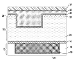
本発明のプロセス・フローは、図6に示される初期相互接続構造体10を準備することで開始する。具体的には、図6に示される初期相互接続構造体10は、誘電体キャッピング層14によって分離される下部相互接続レベル12及び上部相互接続レベル16を含む多重レベル相互接続部を含む。半導体基板(図示せず)の上方に配置することができ、1つ又は複数の半導体デバイスを含む下部相互接続レベル12は、バリア層によって第1の誘電体層18から分離される少なくとも1つの導電性構造部(すなわち、導電性領域)20を有する第1の誘電体材料18を含む。上部相互接続レベル16は、少なくとも1つのライン開口部26が内部に配置された第2の誘電体材料24を含む。示されるように、少なくとも1つのライン開口部26は、第2の誘電体材料内で停止し、下にある導電性構造部20の一部の上方に配置されている。上部相互接続レベル16の上には、パターン形成されたハードマスク28がある。図6に示される構造体は単一のライン開口部26を示すが、本発明は、第2の誘電体材料24内に、第2の誘電体材料24内で停止し、下部相互接続レベル12内に含まれる他の導電性構造部の上に配置される任意の数のこうしたライン開口部を形成することも考慮する。
The process flow of the present invention begins by providing the
図6に示される初期構造体10は、当業者には周知の従来技術を用いて作製される。例えば、初期相互接続構造体は、最初に第1の誘電体材料18を基板(図示せず)の表面に適用することによって形成することができる。基板は、図示されていないが、半導体材料、絶縁材料、導電性材料、又はそれらのいずれかの組み合わせを含むことができる。基板が半導体材料で構成される場合、Si、SiGe、SiGeC、SiC、Ge合金、GaAs、InAs、InP、及び他のIII/V族又はII/VI族化合物半導体のような任意の半導体を用いることができる。これらの列挙されたタイプの半導体材料に加えて、本発明は、半導体基板が、例えばSi/SiGe、Si/SiC、シリコン・オン・インシュレータ(SOI)、又はシリコンゲルマニウム・オン・インシュレータ(SGOI)のような層状半導体である場合も考慮する。
The
基板が絶縁材料である場合、絶縁材料は、有機絶縁体、無機絶縁体、又は多層構造を含むそれらの組み合わせとすることができる。基板が導電性材料である場合、基板は、例えば、ポリSi、元素金属(elemental metal)、元素金属の合金、金属シリサイド、金属窒化物、又は多層構造を含むそれらの組み合わせを含むことができる。基板が半導体材料を含む場合、例えば、相補型金属酸化膜半導体(CMOS)デバイスのような1つ又は複数の半導体デバイスをその上に製造することができる。 When the substrate is an insulating material, the insulating material can be an organic insulator, an inorganic insulator, or a combination thereof including a multilayer structure. If the substrate is a conductive material, the substrate can include, for example, poly-Si, elemental metal, elemental metal alloys, metal silicides, metal nitrides, or combinations thereof including multilayer structures. If the substrate includes a semiconductor material, for example, one or more semiconductor devices such as complementary metal oxide semiconductor (CMOS) devices can be fabricated thereon.
下部相互接続レベル12の第1の誘電体材料18は、無機誘電体又は有機誘電体を含むどのような層間誘電体又は層内誘電体を含んでもよい。第1の誘電体材料18は、多孔性であっても、又は非多孔性であってもよく、本発明の幾つかの実施形態においては、多孔性誘電体は、2.8以下の誘電率を有することが非常に好ましい。第1の誘電体材料18として使用できる好適な誘電体の幾つかの例として、これらに限定されるものではないが、SiO2、シルセスキオキサン、Si、C、O及びH原子を含むCドープ酸化物(すなわち、オルガノシリケート)、熱硬化性ポリアリーレンエーテル、又はそれらの多層構造が挙げられる。「ポリアリーレン」という用語は、本出願においては、結合、縮合環、又は、例えば酸素、硫黄、スルホン、スルホキシド、カルボニルなどのような不活性結合基によって互いに結合された、アリール部分又は不活性置換されたアリール部分を示すために使用される。
The first
第1の誘電体材料18は、典型的には約4.0以下の誘電率を有し、約2.8以下の誘電率がさらにより典型的である。これらの誘電体は、一般に、誘電率が4.0より高い誘電体材料に比べて、寄生クロストークが低い。第1の誘電体材料18の厚さは、使用される誘電体材料、及び下部相互接続レベル12内の誘電体の正確な数に応じて変わり得る。典型的には、通常の相互接続構造体に関して、第1の誘電体材料18は、200nmから450nmまでの厚さを有する。
The first
下部相互接続レベル12はまた、第1の誘電体材料18内に埋め込まれた(すなわち、内部に配置された)少なくとも1つの導電性構造部20も有する。導電性構造部20は、バリア層19によって第1の誘電体材料18から分離される導電性材料を含む。導電性構造部20は、リソグラフィを行ない(すなわち、フォトレジストを第1の誘電体材料18の表面に塗布し、そのフォトレジストを所望の放射パターンに露光し、従来のレジスト現像剤を用いて露光されたレジストを現像する)、第1の誘電体材料18内に開口部をエッチング(乾式エッチング又は湿式エッチング)し、そのエッチングされた領域をバリア層19で、次いで導電性材料で充填して、導電性領域を形成することによって形成される。バリア層19は、Ta、TaN、Ti、TiN、Ru、RuN、W、WN、又は導電性材料がバリア層を通って拡散するのを防止するためのバリアとして作用できる他のいずれかの材料を含むことができ、例えば、原子層堆積(ALD)、化学気相堆積(CVD)、プラズマ強化化学気相堆積(PECVD)、物理気相堆積(PVD)、スパッタリング、化学溶液堆積、又はめっきのような堆積プロセスによって形成される。
The
バリア層19の厚さは、堆積プロセスの正確な手段、並びに使用される材料に応じて変わり得る。典型的には、バリア層19は、4nmから40nmまでの厚さを有し、7nmから20nmまでの厚さがより典型的である。
The thickness of the
バリア層19の形成に続いて、第1の誘電体材料18内の開口部の残りの領域が導電性材料で充填され、導電性構造部20を形成する。導電性構造部20を形成するのに使用される導電性材料は、例えば、ポリSi、導電性金属、少なくとも1つの導電性金属を含む合金、導電性金属シリサイド、又はそれらの組み合わせを含む。導電性構造部20を形成するのに使用される導電性材料は、Cu、W、又はAlのような導電性金属であることが好ましく、本発明においては、Cu又はCu合金(AlCuのような)が非常に好ましい。これらに限定されるものではないが、CVD、PECVD、スパッタリング、化学溶液堆積、又はめっきを含む従来の堆積プロセスを用いて、第1の誘電体材料18内の残りの開口部の中に導電性材料が充填される。これらの堆積の後、例えば、化学機械研磨(CMP)のような従来の平坦化プロセスを用いて、バリア層19及び導電性構造部20のそれぞれが第1の誘電体材料18の上面と実質的に同一平面である上面を有する構造体を提供することができる。
Following the formation of the
少なくとも1つの導電性構造部20を形成した後、例えば、CVD、PECVD、化学溶液堆積、又は蒸着のような従来の堆積プロセスを用いて、下部相互接続レベル12の表面上にブランケット誘電体キャッピング層14が形成される。この誘電体キャッピング層14は、例えば、SiC、Si4NH3、SiO2、炭素ドープ酸化物、窒素及び水素ドープ炭化シリコンSiC(N,H)、又はそれらの多層構造のような、任意の好適な誘電体キャッピング材料を含む。誘電体キャッピング層14の厚さは、これを形成するのに用いられる技術並びに層の材料構成に応じて変わり得る。典型的には、誘電体キャッピング層14は、15nmから55nmまでの厚さを有し、25nmから45nmまでの厚さがより典型的である。
After forming at least one
次に、第2の誘電体材料24を誘電体キャッピング層14の上部露出面に塗布することによって、上部相互接続レベル16が形成される。第2の誘電体材料24は、下部相互接続レベル12の第1の誘電体材料18のものと同じ又は異なる誘電体材料、好ましくは同じ誘電体材料を含むことができる。第1の誘電体材料18に関する処理技術及び厚さの範囲は、第2の誘電体材料24にも適用可能である。第2の誘電体材料24はまた、2つの異なる誘電体材料を含むこともでき、すなわち、最初に1つの誘電体材料を堆積させ、続いて異なる誘電体材料を堆積させることができる。本発明の一実施形態において、第2の誘電体材料24は、2つの異なる低k誘電体材料を含み、従って、上部相互接続レベル16は、多孔性誘電体材料内に埋め込まれた、後で充填される導電性充填ラインと、高密度の(すなわち、非多孔性の)誘電体材料内に埋め込まれた、後で充填されるビアとを有するハイブリッド構造体を有する。このような実施形態において、多孔性低k誘電体は、約2.8以下の誘電率を有し、高密度低k誘電体は、約4.0以下の誘電率を有する。
Next, an
次に、最初に第2の誘電体材料24の上面の上にブランケット・ハードマスク材料を形成することによって、第2の誘電体材料24内に少なくとも1つのライン開口部26が形成される。ブランケット・ハードマスク材料は、酸化物、窒化物、酸窒化物、又はそれらの多層構造を含む任意の組み合わせを含む。典型的には、ハードマスク材料は、SiO2のような酸化物、又はSi3N4のような窒化物である。ブランケット・ハードマスク材料は、例えば、CVD、PECVD、化学溶液堆積、又は蒸着のような従来の堆積プロセスを用いて形成される。堆積されたままのハードマスク材料の厚さは、形成されるハードマスク材料のタイプ、ハードマスク材料を構成する層の数、及びこれを形成するのに用いられる堆積技術に応じて変わり得る。典型的には、堆積されたままのハードマスク材料は、約10nmから約80nmまでの厚さを有し、約20nmから約60nmまでの厚さがさらにより典型的である。
Next, at least one
ハードマスク材料のブランケット層を形成した後、例えば、CVD、PECVD、スピンオン・コーティング、化学溶液堆積、又は蒸着のような従来の堆積プロセスを用いて、ハードマスク材料の上にフォトレジスト(図示せず)が形成される。フォトレジストは、ポジティブ・トーン材料、ネガティブ・トーン材料、又はそれらのハイブリッド材料とすることができ、それらの各々が当業者には周知のものである。次いで、フォトレジストを放射パターンに露光し、従来のレジスト現像剤を用いて露光されたレジストを現像することを含むリソグラフィ・プロセスが、フォトレジストに施される。リソグラフィ・ステップは、ハードマスク材料の上に、ライン開口部26の幅を定めるパターン形成されたフォトレジストを提供する。
After forming the blanket layer of hard mask material, a photoresist (not shown) is formed on the hard mask material using a conventional deposition process such as, for example, CVD, PECVD, spin-on coating, chemical solution deposition, or evaporation. ) Is formed. The photoresist can be a positive tone material, a negative tone material, or a hybrid material thereof, each of which is well known to those skilled in the art. The photoresist is then subjected to a lithographic process that includes exposing the photoresist to a radiation pattern and developing the exposed resist using a conventional resist developer. The lithography step provides a patterned photoresist that defines the width of the
パターン形成されたフォトレジストを提供した後、1つ又は複数のエッチング・プロセスを用いて、ハードマスク材料内に、次いで引き続き第2の誘電体材料24内に、ライン・パターンが転写される。ハードマスク内にライン・パターンを転写し、パターン形成されたハードマスク28を形成した直後、従来の剥離プロセスを用いて、パターン形成されたフォトレジストを剥離することができる。代替的に、最初にライン・パターンをハードマスク内に形成してパターン形成されたハードマスク28を形成し、次に、第2の誘電体材料24内に転写した後に、パターン形成されたフォトレジストを剥離することもできる。ライン・パターンを転写するのに用いられるエッチングは、乾式エッチング・プロセス、湿式化学エッチング・プロセス、又はそれらの組み合わせを含むことができる。ここで用いられる「乾式エッチング」という用語は、反応性イオン・エッチング、イオン・ビーム・エッチング、プラズマ・エッチング、又はレーザ・アブレーションのようなエッチング技術を示すために用いる。
After providing the patterned photoresist, the line pattern is transferred into the hard mask material and then subsequently into the second
図6に示される初期相互接続構造体10を形成した後、次いで、初期相互接続構造体の露出面の全ての上にトレンチ拡散バリア30を形成し、例えば図7に示されるような構造体を提供する。本発明の幾つかの実施形態においては、ライン開口部26内へのトレンチ拡散バリア30の形成は省略され、プロセスは、図8に示される次のステップに続く。こうした実施形態は可能であるが、ライン開口部26内にトレンチ拡散バリアを形成することが好ましい。
After forming the
示されるように、トレンチ拡散バリア30は、パターン形成されたハードマスク28の露出面、及び、ライン開口部26内の第2の誘電体材料24の露出面(例えば、共通の底壁まで延びる側壁)を覆う。本発明によれば、トレンチ拡散バリア30は、その厚さが典型的には0.5nmから20nmまでの範囲内にあり、1nmから10nmまでの厚さがよりいっそう典型的である、薄い層である。トレンチ拡散バリア30は、これらに限定されるものではないが、CVD、PVD、ALD、又はスピンオン・コーティングを含む従来の堆積プロセスを用いて形成される。トレンチ拡散バリア30は、例えば、TaN、Ta、Ti、TiN、RuTa、RuTaN、W、Ru、Co、Rh、又はIr、或いはそれらのいずれかの組み合わせを含む、金属拡散に対して耐性があるいずれかの材料を含む層又は材料スタックを含む。
As shown, the
次に、図8に示されるように、ライン開口部26を充填し、パターン形成されたマスク28の表面上に位置するトレンチ拡散バリア30の上方に延びるように、平坦化層32が堆積される。トレンチ誘電体30が使用されない実施形態においては、平坦化層32は、第2の誘電体材料24の露出した壁部分、及び、パターン形成されたハードマスク28の上面に直接接触する。
Next, as shown in FIG. 8, a
平坦化層32は、例えば、CVD、PECVD、スピンオン・コーティング、蒸着、又は化学溶液堆積を含む従来の堆積プロセスを用いて堆積される。平坦化材料は、従来の反射防止コーティング材料又はスパンガラス材料を含む。
The
さらに図8を参照すると、平坦化層32を形成した後、次いで、平坦化層32の表面の上に、低温酸化物などの酸化物含有層34が形成される。酸化物含有層34は、これらに限定されるものではないが、堆積温度が500℃より低いCVD及びPECVDを含むいずれかの従来の堆積プロセスを用いて形成される。酸化物含有層34は、典型的には5nmから100nmまでの厚さを有し、20nmから50nmまでの厚さがより典型的である。
Still referring to FIG. 8, after forming the
次に、堆積及びリソグラフィによって、酸化物含有層34の上面上に、ビア開口部パターンを含むパターン形成されたフォトレジスト(具体的には示されない)が形成される。次いで、ビア開口部のパターンを、パターン形成されたフォトレジストから少なくとも酸化物含有層34内に転写するエッチング・ステップが行なわれる。ビア開口部パターンの転写は、ライン開口部26を第2の誘電体材料24内に形成する際の上述したエッチング・ステップのうちの1つを用いて行なわれる。ビア・パターンを酸化物含有層34内に転写した後、例えばアッシング(ashing)のような従来のレジスト剥離プロセスを用いて、パターン形成されたフォトレジストが剥離される。これらのステップを行なった後に形成される結果として得られる構造体が、例えば、図9に示される。図9において、パターン形成された酸化物含有層は、参照番号34’で表され、初期ビア開口部は、参照番号36で表される。
Next, a patterned photoresist (not specifically shown) including a via opening pattern is formed on the top surface of the oxide-containing layer 34 by deposition and lithography. An etching step is then performed to transfer the pattern of via openings from the patterned photoresist into at least the oxide-containing layer 34. Transfer of the via opening pattern is performed using one of the etching steps described above in forming the
次に、図10に示されるように、初期ビア開口部36が、平坦化層32の一部、存在する場合はトレンチ拡散バリア30の一部、及び下にある第2の誘電体材料24の一部を通って下方に延び、誘電体キャッピング層14の表面の上で停止し、拡張されたビア開口部36’を形成する。幾つかの実施形態においては、エッチング・ステップは、誘電体キャッピング層14の一部をパンチスルーする(punch through)、すなわち除去し、導電性構造部20の表面の上で停止することができる。初期ビア開口部36の延長は、図10に示される構造体を形成できる1つ又は複数のエッチング・プロセスを含む。示されるように、少なくとも残りの平坦化層32によって保護されるライン開口部26は、拡張されたビア開口部36’の上方に配置され、これに接続される。1つ又は複数のエッチング・ステップ中、図10に示されるように、パターン形成された酸化物含有層34’も除去されることが認められる。
Next, as shown in FIG. 10, an initial via opening 36 is part of the
次に、最初に誘電体キャッピング層14を開口するかどうかに関係なく、図10に示される構造体にArスパッタリング・プロセスを施し、このArスパッタリング・プロセスにより、前もって除去されていない場合には、拡張されたビア開口部36’の底部から誘電体キャッピング層の一部を除去し、下にある導電性構造部20をパンチスルーして、導電性構造部20内にガウジング構造部(すなわち、アンカー領域)38を生成する。Arスパッタリングの後に結果として得られる構造体が、例えば、図11に示される。第2の誘電体材料24は、少なくとも残りの平坦化層32、存在する場合にはトレンチ拡散バリア30及びパターン形成されたハードマスク層28によって保護されているので、このプロセス中に損傷を受けない。
Next, regardless of whether the
ガウジング構造部38を形成するのに用いられるArスパッタリング・プロセスは、こうした構造部を形成するために相互接続技術において典型的に用いられる任意の従来のArスパッタリング・プロセスを含む。例証として、Arスパッタリングは、次の限定されない条件、すなわち20sccmのArガス流、25℃の温度、400KHz及び750Wの上部電極バイアス、13.6MHz及び400Wのテーブルバイアス、並びに0.6mtorrのプロセス圧力を用いて行なうことができる。説明のためにArが示されているが、スパッタリング・プロセスのために、He、Ne、Xe、N2、H2、NH3、N2H2、又はそれらの混合物のような他の任意のガスを用いることもできる。
The Ar sputtering process used to form the
本発明の幾つかの実施形態(具体的には示されない)においては、導電性構造部20の少なくともガウジングされた表面上に金属界面層を形成することができる。存在する場合、金属界面層は、例えば、CVD、PECVD、化学溶液堆積、蒸着、有機金属堆積、ALD、スパッタリング、PVD、又はめっき(無電解又は電解)を含む、任意の従来の堆積プロセスを用いて形成される。金属界面層の厚さは、使用される正確な金属界面材料、及び、金属界面層を形成するのに用いられる堆積技術に応じて変わり得る。典型的には、金属界面層は、0.5nmから40nmまでの厚さを有し、1nmから10nmまでの厚さがさらにより典型的である。金属界面層は、例えば、Co、TaN、Ta、Ti、TiN、Ru、Ir、Au、Rh、Pt、Pd、又はAgなどの金属バリア材料を含む。こうした材料の合金も考慮される。
In some embodiments (not specifically shown) of the present invention, a metal interface layer can be formed on at least the gouged surface of the
図12は、残りの平坦化層32がライン開口部26内から剥離された後の、図11の構造体を示す。残りの平坦化層32の剥離は、化学湿式エッチング・プロセス、又は構造体から平坦化材料を選択的に除去する化学アッシング・プロセスのいずれかを用いて行なわれる。
FIG. 12 shows the structure of FIG. 11 after the remaining
本発明の幾つかの実施形態においては、酸化物又はエッチング残留物(図示せず)が、ガウジング構造部38内に残ることがある。このような場合、酸化物又はエッチング残留物は、化学湿式エッチング・プロセス及び/又は少量のAr衝撃(bombardment)を含むことができる表面洗浄プロセスを用いて、ガウジング構造部38から除去することができる。Ar衝撃の条件は、ガウジング構造部38を形成するのに用いられるものほど厳しくないので、この場合、損傷は生じない。典型的には、この場合に用いられる表面洗浄だけのためのプロセス時間は、従来技術において用いられる、ガウジング構造部を生成するための10秒以上に比べて、5秒未満である。例証として、Arスパッタリングは、次の限定されない条件、すなわち20sccmのArガス流、25℃の温度、400KHz及び400Wの上部電極バイアス、13.6MHz及び200Wのテーブルバイアス、及び0.6mtorrのプロセス圧力を用いて行なうことができる。説明のためにArが示されたが、スパッタリング・プロセスのために、He、Ne、Xe、N2、H2、NH3、N2H2、又はそれらの混合物のような任意の他のガスを用いることもできる。
In some embodiments of the present invention, oxide or etch residues (not shown) may remain in the
本発明の幾つかの実施形態において、エッチング残留物が、少なくても1つのライン開口部26及び少なくとも拡張されたビア開口部36’から除去される。1つの実施形態においては、O2、H2、N2、CO、CO2、又はNH3の少なくとも1つ又は組み合わせを含むプラズマ・エッチングが用いられる。別の実施形態においては、エッチング残留物は、HF、HCI、H2SO4、又はHNO3の少なくとも1つ又は組み合わせを含む湿式洗浄によって除去される。
In some embodiments of the present invention, etch residues are removed from at least one
本発明の方法のこの時点で、組み合わされたトレンチ及びビア拡散バリア40が、図12に示される構造体内に形成され、図13に示される構造体を提供する。示されるように、組み合わされたトレンチ及びビア拡散バリア40は、ライン開口部26及拡張されたビア開口部36’の両方の中に存在し、一方、存在する場合、トレンチ拡散バリア30は、ライン開口部26内にのみ存在する。トレンチ拡散バリア30が存在するとき、組み合わされたトレンチ及びビア拡散バリア40は、ライン開口部内のトレンチ拡散バリア30の上、拡張されたビア開口部36’内の第2の誘電体材料24の露出された壁面の上、及び導電性構造部20のガウジングされた面の上に配置される。
At this point in the method of the present invention, a combined trench and via
組み合わされたトレンチ及びビア拡散バリア40は、導電性材料がそこを通って拡散するのを防止するためのバリアとして作用できるいずれかの材料を含む。例証として、組み合わされたトレンチ及びビア拡散バリア40は、TaN、Ta、Ti、TiN、RuTa、RuTaN、W、Ru、Co、Rh、又はIr、或いはそれらの任意の組み合わせの層又は材料スタックを含む。組み合わされたトレンチ及びビア拡散バリア層40は、トレンチ拡散バリア30とは異なる層又は材料スタックを表すことが認められる。
The combined trench and via
組み合わされたトレンチ及びビア拡散バリア40は、ライン開口部及び拡張されたビア開口部の両方の中に存在する連続的な層であり、例えば、原子層堆積(ALD)、化学気相堆積(CVD)、プラズマ強化化学気相堆積(PECVD)、物理気相堆積(PVD)、スパッタリング、化学溶液堆積、又はめっきなどの堆積プロセスを用いて形成される。
The combined trench and via
組み合わされたトレンチ及びビア拡散バリア40の厚さは、バリア内の材料層の数、拡散バリアを形成するのに使用される技術、並びに拡散バリア自体の材料に応じて変わり得る。典型的には、組み合わされたトレンチ及びビア拡散バリア40は、4nmから40nmまでの厚さを有し、7nmから20nmまでの厚さがさらにより典型的である。
The thickness of the combined trench and via
本発明の幾つかの実施形態においては、ここで、図13に示される構造体内にめっきシード層(図示せず)が形成される。使用される場合、このめっきシード層は、Cu、或いは元素周期表のVIIIA族からの金属又は金属合金から成る。めっきシード層のための好適なVIIIA族元素の例として、これらに限定されるものではないが、Ru、TaRu、Ir、Rh、Pt、Pd及びそれらの合金が挙げられる。幾つかの実施形態においては、めっきシード層としてCu、Ru、Ir、又はRhを用いることが好ましい。 In some embodiments of the present invention, a plating seed layer (not shown) is now formed within the structure shown in FIG. If used, this plating seed layer is made of Cu or a metal or metal alloy from Group VIIIA of the Periodic Table of Elements. Examples of suitable Group VIIIA elements for the plating seed layer include, but are not limited to, Ru, TaRu, Ir, Rh, Pt, Pd, and alloys thereof. In some embodiments, it is preferable to use Cu, Ru, Ir, or Rh as the plating seed layer.
めっきシード層は、例えば、化学気相堆積(CVD)、プラズマ強化化学気相堆積(PECVD)、原子層堆積(ALD)、めっき、スパッタリング、及び物理気相堆積(PVP)を含む従来の堆積プロセスによって形成される。めっきシード層の厚さは、例えば、めっきシード層の組成材料、及びめっきシード層を形成するのに使用された技術を含む多数の要因に応じて変わり得る。典型的には、めっきシード層は、約0.5nmから約10nmまでの厚さを有し、6nm未満の厚さがさらにより典型的である。 The plating seed layer is a conventional deposition process including, for example, chemical vapor deposition (CVD), plasma enhanced chemical vapor deposition (PECVD), atomic layer deposition (ALD), plating, sputtering, and physical vapor deposition (PVP). Formed by. The thickness of the plating seed layer can vary depending on a number of factors including, for example, the composition material of the plating seed layer and the technique used to form the plating seed layer. Typically, the plating seed layer has a thickness from about 0.5 nm to about 10 nm, with a thickness of less than 6 nm being even more typical.
次に、図13に示される構造体は、めっきシード層の有無に関係なく、相互接続導電性材料42で充填され、平坦化されて、図14に示される平坦化された構造体を提供する。示されるように、相互接続導電性材料は、拡張されたビア開口部36’、ライン開口部26、並びにガウジング構造部38を充填する。相互接続導電性材料42は、導電性構造部20のものと同じ又は異なる導電性材料、好ましくは同じ導電性材料を含むことができる。Cu、Al、W、又はそれらの合金が使用されることが好ましく、Cu又はAlCuが最も好ましい。相互接続導電性材料42は、導電性構造部20を形成する際に上述されたものと同じ堆積プロセスを用いて形成され、導電性材料の堆積に続いて、構造体に平坦化が施される。化学機械研磨及び/又は研削を含む平坦化プロセスにより、上部相互接続レベル16の第2の誘電体材料24の上に配置された、例えば組み合わされたトレンチ及びビア拡散バリア40、トレンチ拡散バリア30、及びパターン形成されたハードマスク28などの種々の材料が除去される。
Next, the structure shown in FIG. 13 is filled with the interconnect
本出願の方法は、図14に示されるレベルの上に付加的な相互接続レベルを形成するのにも適用可能である。種々の相互接続レベルの各々が、前述のガウジング構造部を含む。 The method of the present application is also applicable to form additional interconnect levels above the levels shown in FIG. Each of the various interconnect levels includes the aforementioned gouging structure.
上述の統合処理スキームのために、ガウジング構造部38の形成中、第2の誘電体材料24内に損傷領域は形成されない。
Due to the integrated processing scheme described above, no damaged areas are formed in the second
本発明をその好ましい実施形態について特に示し、説明したが、当業者であれば、本発明の精神及び範囲から逸脱することなく、形態及び細部について前述及び他の変更をなし得ることを理解するであろう。従って、本発明は、説明され図示された通りの正確な形態及び細部に限定されるものではなく、添付の特許請求の範囲内であることが意図される。 While the invention has been particularly shown and described with respect to preferred embodiments thereof, those skilled in the art will recognize that these and other changes may be made in form and detail without departing from the spirit and scope of the invention. I will. Accordingly, the invention is not limited to the precise forms and details as described and illustrated, but is intended to be within the scope of the following claims.
10:初期相互接続構造体
12:下部相互接続レベル
14:誘電体キャッピング層
16:上部相互接続レベル
18:第1の誘電体材料
19:バリア層
20:導電性構造部
24:第2の誘電体材料
26:ライン開口部
28:パターン形成されたハードマスク
30:トレンチ拡散バリア
32:平坦化層
34:酸化物含有層
34’:パターン形成された酸化物含有層
36:初期ビア開口部
36’:拡張されたビア開口部
38:ガウジング構造部(アンカー領域)
40:組み合わされたトレンチ及びビア拡散バリア
42:相互接続導電性材料
10: Initial interconnect structure 12: Lower interconnect level 14: Dielectric capping layer 16: Upper interconnect level 18: First dielectric material 19: Barrier layer 20: Conductive structure 24: Second dielectric Material 26: Line opening 28: Patterned hard mask 30: Trench diffusion barrier 32: Planarization layer 34: Oxide-containing layer 34 ′: Patterned oxide-containing layer 36: Initial via opening 36 ′: Expanded via opening 38: gouging structure (anchor region)
40: Combined trench and via diffusion barrier 42: Interconnect conductive material
Claims (20)
前記第1の誘電体材料及び前記少なくとも1つの導電性構造部の全てではなく一部分の上に配置された誘電体キャッピング層と、
少なくとも1つの導電性充填ビア及び上にある導電性充填ラインが内部に配置された第2の誘電体材料を含む上部相互接続レベルであって、前記少なくとも1つの導電性充填ビアは、ガウジング構造部によって前記下部相互接続レベルの前記少なくとも1つの導電性構造部の露出面と接触しており、前記少なくとも1つの導電性充填ラインは、前記少なくとも1つの導電性充填ラインを前記第2の誘電体材料の上部から分離する、トレンチ拡散バリアと、組み合わされたトレンチ及びビア拡散バリアとを含み、一方、前記少なくとも1つの導電性充填ビアは、前記少なくとも1つの導電性充填ビアの下部と前記第2の誘電体材料を分離する前記組み合わされたトレンチ及びビア拡散バリアのみを含み、前記組み合わされたトレンチ及びビア拡散バリアは、前記少なくとも1つの導電性充填ビアの下部と前記第1の誘電体材料内に埋め込まれた前記少なくとも1つの導電性構造部との間の前記ガウジング構造部にも配置される、上部相互接続レベルと、
を含む半導体相互接続構造体。 A lower interconnect level comprising a first dielectric material having at least one conductive structure embedded therein;
A dielectric capping layer disposed on a portion but not all of the first dielectric material and the at least one conductive structure;
An upper interconnect level comprising at least one conductive fill via and a second dielectric material having an overlying conductive fill line disposed therein, the at least one conductive fill via comprising a gouging structure In contact with an exposed surface of the at least one conductive structure at the lower interconnect level, wherein the at least one conductive fill line replaces the at least one conductive fill line with the second dielectric material. A trench diffusion barrier and a combined trench and via diffusion barrier separated from an upper portion of the at least one conductive fill via, wherein the at least one conductive fill via and the second lower portion of the at least one conductive fill via Including only the combined trench and via diffusion barrier separating the dielectric material, the combined trench and via extension. A barrier is also disposed on the gouging structure between the lower part of the at least one conductive filling via and the at least one conductive structure embedded in the first dielectric material. Connection level,
A semiconductor interconnect structure comprising:
少なくとも1つの導電性構造部が内部に埋め込まれた第1の誘電体材料と、前記第1の誘電体材料の上方に配置された第2の誘電体材料とを含む構造体を準備するステップであって、前記第1の誘電体材料は、トレンチ拡散バリアでライニングされた少なくとも1つのライン開口部が内部に配置されている、ステップと、
前記第2の誘電体材料内に少なくとも1つの拡張されたビア開口部を形成するステップと、
前記少なくとも1つの導電性構造部内に少なくとも1つのガウジング構造部を形成するステップと、
前記少なくとも1つのライン開口部及び前記少なくとも1つの拡張されたビア開口部内、及び、前記少なくとも1つのガウジング構造部の上に、組み合わされたトレンチ及びビア拡散バリアを形成するステップと、
前記少なくとも1つのライン開口部及び前記少なくとも1つのビア開口部を相互接続導電性材料で充填するステップと、
を含む方法。 A method of forming a semiconductor interconnect structure, comprising:
Providing a structure including a first dielectric material having at least one conductive structure embedded therein and a second dielectric material disposed above the first dielectric material; The first dielectric material has at least one line opening lined therein with a trench diffusion barrier; and
Forming at least one extended via opening in the second dielectric material;
Forming at least one gouging structure in the at least one conductive structure;
Forming a combined trench and via diffusion barrier in the at least one line opening and the at least one extended via opening and on the at least one gouging structure;
Filling the at least one line opening and the at least one via opening with an interconnecting conductive material;
Including methods.
前記少なくとも1つのライン開口部内、及び、前記第2の誘電体材料の上に、平坦化材料を形成するステップと、
前記平坦化材料の上面上にパターン形成された酸化物含有材料を形成するステップであって、前記パターン形成された酸化物含有材料は、少なくとも1つの初期ビア・パターンを内部に有する、ステップと、
前記少なくとも1つの平坦化層、前記トレンチ拡散バリア及び前記第2の誘電体材料を通って前記少なくとも1つの初期ビア・パターンを延ばし、前記第2の誘電体材料内に前記少なくとも1つの拡張されたビア開口部を提供するステップと、
を含む、請求項11に記載の方法。 The step of forming the at least one extended via opening comprises:
Forming a planarizing material in the at least one line opening and on the second dielectric material;
Forming a patterned oxide-containing material on an upper surface of the planarizing material, the patterned oxide-containing material having at least one initial via pattern therein;
Extending the at least one initial via pattern through the at least one planarization layer, the trench diffusion barrier and the second dielectric material, and extending the at least one into the second dielectric material. Providing a via opening;
12. The method of claim 11 comprising:
少なくとも1つの導電性構造部が内部に埋め込まれた第1の誘電体材料と、前記第1の誘電体材料の上方に配置された第2の誘電体材料とを含む構造体を準備するステップであって、前記第1の誘電体材料は少なくとも1つのライン開口部を有する、ステップと、
前記第2の誘電体材料内に少なくとも1つの拡張されたビア開口部を形成するステップと、
前記少なくとも1つの導電性構造部内に少なくとも1つのガウジング構造部を形成するステップと、
前記少なくとも1つのライン開口部及び前記少なくとも1つの拡張されたビア開口部内、及び、前記少なくとも1つのガウジング構造部の上に、組み合わされたトレンチ及びビア拡散バリアを形成するステップと、
前記少なくとも1つのライン開口部及び前記少なくとも1つのビア開口部を相互接続導電性材料で充填するステップと、
を含む方法。 A method of forming a semiconductor interconnect structure, comprising:
Providing a structure including a first dielectric material having at least one conductive structure embedded therein and a second dielectric material disposed above the first dielectric material; The first dielectric material has at least one line opening; and
Forming at least one extended via opening in the second dielectric material;
Forming at least one gouging structure in the at least one conductive structure;
Forming a combined trench and via diffusion barrier in the at least one line opening and the at least one extended via opening and on the at least one gouging structure;
Filling the at least one line opening and the at least one via opening with an interconnecting conductive material;
Including methods.
前記少なくとも1つのライン開口部内、及び、前記第2の誘電体材料の上に、平坦化材料を形成するステップと、
前記平坦化材料の上面上にパターン形成された酸化物含有材料を形成するステップであって、前記パターン形成された酸化物含有材料は、少なくとも1つの初期ビア・パターンを内部に有する、ステップと、
前記少なくとも1つの平坦化層及び前記第2の誘電体材料を通って前記少なくとも1つの初期ビア・パターンを延ばし、前記第2の誘電体材料内に前記少なくとも1つの拡張されたビア開口部を提供するステップと、
を含む、請求項16に記載の方法。 The step of forming the at least one extended via opening comprises:
Forming a planarizing material in the at least one line opening and on the second dielectric material;
Forming a patterned oxide-containing material on an upper surface of the planarizing material, the patterned oxide-containing material having at least one initial via pattern therein;
Extending the at least one initial via pattern through the at least one planarization layer and the second dielectric material to provide the at least one extended via opening in the second dielectric material And steps to
The method of claim 16 comprising:
Applications Claiming Priority (1)
| Application Number | Priority Date | Filing Date | Title |
|---|---|---|---|
| US12/494,564 US7964966B2 (en) | 2009-06-30 | 2009-06-30 | Via gouged interconnect structure and method of fabricating same |
Publications (2)
| Publication Number | Publication Date |
|---|---|
| JP2011014904A true JP2011014904A (en) | 2011-01-20 |
| JP2011014904A5 JP2011014904A5 (en) | 2013-10-03 |
Family
ID=43379790
Family Applications (1)
| Application Number | Title | Priority Date | Filing Date |
|---|---|---|---|
| JP2010142938A Pending JP2011014904A (en) | 2009-06-30 | 2010-06-23 | Via gouged interconnect structure, and method of fabricating the same |
Country Status (3)
| Country | Link |
|---|---|
| US (1) | US7964966B2 (en) |
| JP (1) | JP2011014904A (en) |
| KR (1) | KR20110001894A (en) |
Families Citing this family (20)
| Publication number | Priority date | Publication date | Assignee | Title |
|---|---|---|---|---|
| KR20110003191A (en) * | 2009-07-03 | 2011-01-11 | 삼성전자주식회사 | Device Separation and Method of Forming Semiconductor Device |
| US9177917B2 (en) * | 2010-08-20 | 2015-11-03 | Micron Technology, Inc. | Semiconductor constructions |
| US9054110B2 (en) * | 2011-08-05 | 2015-06-09 | Taiwan Semiconductor Manufacturing Company, Ltd. | Low-K dielectric layer and porogen |
| US8835305B2 (en) | 2012-07-31 | 2014-09-16 | International Business Machines Corporation | Method of fabricating a profile control in interconnect structures |
| US8749060B2 (en) * | 2012-09-21 | 2014-06-10 | Taiwan Semiconductor Manufacturing Company, Ltd. | Method of semiconductor integrated circuit fabrication |
| US9030013B2 (en) * | 2012-09-21 | 2015-05-12 | Taiwan Semiconductor Manufacturing Company, Ltd. | Interconnect structures comprising flexible buffer layers |
| US10043706B2 (en) * | 2013-01-18 | 2018-08-07 | Taiwan Semiconductor Manufacturing Company Limited | Mitigating pattern collapse |
| US10032712B2 (en) * | 2013-03-15 | 2018-07-24 | Taiwan Semiconductor Manufacturing Company Limited | Semiconductor structure |
| CN104078445A (en) * | 2013-03-29 | 2014-10-01 | 联华电子股份有限公司 | Plug structure and its manufacturing process |
| US9349691B2 (en) | 2014-07-24 | 2016-05-24 | International Business Machines Corporation | Semiconductor device with reduced via resistance |
| US9991200B2 (en) | 2014-09-25 | 2018-06-05 | Taiwan Semiconductor Manufacturing Company, Ltd. | Air gap structure and method |
| US9685370B2 (en) | 2014-12-18 | 2017-06-20 | Globalfoundries Inc. | Titanium tungsten liner used with copper interconnects |
| US10211148B2 (en) * | 2015-12-14 | 2019-02-19 | International Business Machines Corporation | Structural enhancement of Cu nanowires |
| US9935051B2 (en) | 2016-08-18 | 2018-04-03 | International Business Machines Corporation | Multi-level metallization interconnect structure |
| JP2018107227A (en) * | 2016-12-26 | 2018-07-05 | ソニーセミコンダクタソリューションズ株式会社 | SEMICONDUCTOR DEVICE, SEMICONDUCTOR DEVICE MANUFACTURING METHOD, AND SOLID-STATE IMAGING ELEMENT |
| KR102718741B1 (en) * | 2016-12-29 | 2024-10-18 | 인텔 코포레이션 | Self-aligned via |
| US11018054B2 (en) | 2017-04-12 | 2021-05-25 | Intel Corporation | Integrated circuit interconnects |
| KR102438179B1 (en) * | 2017-11-02 | 2022-08-30 | 삼성전자주식회사 | Semiconductor devices and semiconductor packages including the same, and methods of manufacturing the semiconductor devices |
| US20200111741A1 (en) * | 2018-10-09 | 2020-04-09 | International Business Machines Corporation | Vertical electrical fuse |
| US11177169B2 (en) * | 2019-06-21 | 2021-11-16 | International Business Machines Corporation | Interconnects with gouged vias |
Citations (4)
| Publication number | Priority date | Publication date | Assignee | Title |
|---|---|---|---|---|
| WO2008036115A1 (en) * | 2006-03-01 | 2008-03-27 | International Business Machines Corporation | Novel structure and method for metal integration |
| US20080128907A1 (en) * | 2006-12-01 | 2008-06-05 | International Business Machines Corporation | Semiconductor structure with liner |
| JP2008543078A (en) * | 2005-05-31 | 2008-11-27 | アドバンスト・マイクロ・ディバイシズ・インコーポレイテッド | Technique for forming a copper-containing wire embedded in a low-k dielectric by providing a reinforcing layer |
| JP2009027048A (en) * | 2007-07-23 | 2009-02-05 | Panasonic Corp | Manufacturing method of semiconductor device |
Family Cites Families (3)
| Publication number | Priority date | Publication date | Assignee | Title |
|---|---|---|---|---|
| JP5162869B2 (en) * | 2006-09-20 | 2013-03-13 | 富士通セミコンダクター株式会社 | Semiconductor device and manufacturing method thereof |
| US7846834B2 (en) * | 2008-02-04 | 2010-12-07 | International Business Machines Corporation | Interconnect structure and method for Cu/ultra low k integration |
| US7834457B2 (en) * | 2008-02-28 | 2010-11-16 | International Business Machines Corporation | Bilayer metal capping layer for interconnect applications |
-
2009
- 2009-06-30 US US12/494,564 patent/US7964966B2/en active Active
-
2010
- 2010-06-18 KR KR1020100057973A patent/KR20110001894A/en not_active Application Discontinuation
- 2010-06-23 JP JP2010142938A patent/JP2011014904A/en active Pending
Patent Citations (5)
| Publication number | Priority date | Publication date | Assignee | Title |
|---|---|---|---|---|
| JP2008543078A (en) * | 2005-05-31 | 2008-11-27 | アドバンスト・マイクロ・ディバイシズ・インコーポレイテッド | Technique for forming a copper-containing wire embedded in a low-k dielectric by providing a reinforcing layer |
| WO2008036115A1 (en) * | 2006-03-01 | 2008-03-27 | International Business Machines Corporation | Novel structure and method for metal integration |
| JP2009528702A (en) * | 2006-03-01 | 2009-08-06 | インターナショナル・ビジネス・マシーンズ・コーポレーション | Novel structure and method for metal integration |
| US20080128907A1 (en) * | 2006-12-01 | 2008-06-05 | International Business Machines Corporation | Semiconductor structure with liner |
| JP2009027048A (en) * | 2007-07-23 | 2009-02-05 | Panasonic Corp | Manufacturing method of semiconductor device |
Also Published As
| Publication number | Publication date |
|---|---|
| US7964966B2 (en) | 2011-06-21 |
| US20100327446A1 (en) | 2010-12-30 |
| KR20110001894A (en) | 2011-01-06 |
Similar Documents
| Publication | Publication Date | Title |
|---|---|---|
| JP5430946B2 (en) | Interconnect structure forming method | |
| US7964966B2 (en) | Via gouged interconnect structure and method of fabricating same | |
| JP5462807B2 (en) | Interconnect structure with high leakage resistance | |
| US8354751B2 (en) | Interconnect structure for electromigration enhancement | |
| US7867895B2 (en) | Method of fabricating improved interconnect structure with a via gouging feature absent profile damage to the interconnect dielectric | |
| US7834457B2 (en) | Bilayer metal capping layer for interconnect applications | |
| JP5255292B2 (en) | Interconnect structure having two-layer metal cap and method of manufacturing the same | |
| US8232196B2 (en) | Interconnect structure having a via with a via gouging feature and dielectric liner sidewalls for BEOL integration | |
| JP5419328B2 (en) | Interconnect structure having redundant barrier components and method of forming an interconnect structure | |
| JP5818210B2 (en) | Interconnect structure having interface layer with improved electromigration resistance of dielectric line vias and method of manufacturing the same | |
| US7846834B2 (en) | Interconnect structure and method for Cu/ultra low k integration | |
| JP5385610B2 (en) | Method for forming an interconnect structure | |
| US20080128907A1 (en) | Semiconductor structure with liner | |
| KR20100098673A (en) | Noble metal cap for interconnect structures | |
| KR20110083636A (en) | Discrete / Uneven Metal Cap Structure and Process for Wiring Integration | |
| KR100632038B1 (en) | Method of manufacturing multilayer metal wiring | |
| JP2005129746A (en) | Semiconductor device and manufacturing method thereof |
Legal Events
| Date | Code | Title | Description |
|---|---|---|---|
| A621 | Written request for application examination |
Free format text: JAPANESE INTERMEDIATE CODE: A621 Effective date: 20130301 |
|
| RD12 | Notification of acceptance of power of sub attorney |
Free format text: JAPANESE INTERMEDIATE CODE: A7432 Effective date: 20130801 |
|
| A521 | Written amendment |
Free format text: JAPANESE INTERMEDIATE CODE: A523 Effective date: 20130805 |
|
| A871 | Explanation of circumstances concerning accelerated examination |
Free format text: JAPANESE INTERMEDIATE CODE: A871 Effective date: 20130805 |
|
| A521 | Written amendment |
Free format text: JAPANESE INTERMEDIATE CODE: A821 Effective date: 20130801 |
|
| A975 | Report on accelerated examination |
Free format text: JAPANESE INTERMEDIATE CODE: A971005 Effective date: 20130924 |
|
| A131 | Notification of reasons for refusal |
Free format text: JAPANESE INTERMEDIATE CODE: A131 Effective date: 20131022 |
|
| A601 | Written request for extension of time |
Free format text: JAPANESE INTERMEDIATE CODE: A601 Effective date: 20140120 |
|
| A602 | Written permission of extension of time |
Free format text: JAPANESE INTERMEDIATE CODE: A602 Effective date: 20140123 |
|
| RD14 | Notification of resignation of power of sub attorney |
Free format text: JAPANESE INTERMEDIATE CODE: A7434 Effective date: 20140216 |
|
| A02 | Decision of refusal |
Free format text: JAPANESE INTERMEDIATE CODE: A02 Effective date: 20140507 |