JP2010257528A - Semiconductor integrated circuit device - Google Patents
Semiconductor integrated circuit device Download PDFInfo
- Publication number
- JP2010257528A JP2010257528A JP2009106671A JP2009106671A JP2010257528A JP 2010257528 A JP2010257528 A JP 2010257528A JP 2009106671 A JP2009106671 A JP 2009106671A JP 2009106671 A JP2009106671 A JP 2009106671A JP 2010257528 A JP2010257528 A JP 2010257528A
- Authority
- JP
- Japan
- Prior art keywords
- voltage generation
- planes
- circuit
- semiconductor integrated
- power supply
- Prior art date
- Legal status (The legal status is an assumption and is not a legal conclusion. Google has not performed a legal analysis and makes no representation as to the accuracy of the status listed.)
- Pending
Links
- 239000004065 semiconductor Substances 0.000 title claims abstract description 44
- 230000000052 comparative effect Effects 0.000 description 18
- 230000000630 rising effect Effects 0.000 description 11
- 230000008859 change Effects 0.000 description 8
- 238000010586 diagram Methods 0.000 description 8
- 230000000694 effects Effects 0.000 description 8
- 239000000470 constituent Substances 0.000 description 4
- 238000013500 data storage Methods 0.000 description 4
- 238000004364 calculation method Methods 0.000 description 3
- 230000006866 deterioration Effects 0.000 description 3
- 238000004904 shortening Methods 0.000 description 3
- 239000000758 substrate Substances 0.000 description 3
- 230000006870 function Effects 0.000 description 2
- 238000001459 lithography Methods 0.000 description 2
- 230000001737 promoting effect Effects 0.000 description 2
- 238000009825 accumulation Methods 0.000 description 1
- 230000004913 activation Effects 0.000 description 1
- 230000008901 benefit Effects 0.000 description 1
- 230000007547 defect Effects 0.000 description 1
- 230000002542 deteriorative effect Effects 0.000 description 1
- 230000004048 modification Effects 0.000 description 1
- 238000012986 modification Methods 0.000 description 1
Images


Classifications
-
- G—PHYSICS
- G11—INFORMATION STORAGE
- G11C—STATIC STORES
- G11C5/00—Details of stores covered by group G11C11/00
- G11C5/14—Power supply arrangements, e.g. power down, chip selection or deselection, layout of wirings or power grids, or multiple supply levels
- G11C5/145—Applications of charge pumps; Boosted voltage circuits; Clamp circuits therefor
-
- G—PHYSICS
- G11—INFORMATION STORAGE
- G11C—STATIC STORES
- G11C16/00—Erasable programmable read-only memories
- G11C16/02—Erasable programmable read-only memories electrically programmable
- G11C16/06—Auxiliary circuits, e.g. for writing into memory
- G11C16/30—Power supply circuits
Landscapes
- Engineering & Computer Science (AREA)
- Power Engineering (AREA)
- Read Only Memory (AREA)
Abstract
Description
この発明は、半導体集積回路装置に関し、例えば、NAND型フラッシュメモリ等に適用可能なものである。 The present invention relates to a semiconductor integrated circuit device, and can be applied to, for example, a NAND flash memory.
例えば、NAND型フラッシュメモリは、大容量かつ不揮発という利点を生かし、近年では、携帯オーディオ機器をはじめ、様々な電子機器のメモリとして搭載されている。 For example, a NAND flash memory takes advantage of its large capacity and non-volatility, and has recently been mounted as a memory for various electronic devices including portable audio devices.
このような状況の下、NAND型フラッシュメモリは、その機能の向上に加えて、さらなる大容量化が今後の課題となっている。ここで、大容量化を実現するためには、メモリセルの微細化を推し進めつつ、ワード線、ビット線長の増大による特性劣化を抑制するために、メモリセルアレイを複数プレーン(Plane)化することが有望であると考えられている。 Under such circumstances, in addition to improving the functions of the NAND flash memory, further increase in capacity is a future issue. Here, in order to increase the capacity, the memory cell array should be made into a plurality of planes in order to suppress the deterioration of characteristics due to the increase of the word line and bit line length while promoting the miniaturization of the memory cells. Is considered promising.
しかしながら、2プレーン以上の複数プレーン化が進行すると、選択プレーン数の変化に伴って負荷容量が変動するため、充電時間が選択プレーン数により大きく変動する。そのため、動作マージンの悪化を引き起こす。 However, when the number of planes is increased to two or more, the load capacity varies with the change in the number of selected planes, so the charging time varies greatly depending on the number of selected planes. Therefore, the operation margin is deteriorated.
この発明の一態様に係る半導体集積回路装置は、それぞれが複数のメモリセルを有する複数のプレーンを備えるメモリセルアレイと、一定の供給能力を保つ共通電圧発生回路と、前記複数のプレーンの数に対応して配置される複数の電圧発生回路とを備える電源電圧発生回路と、前記電源電圧発生回路を制御する制御回路とを具備する。 A semiconductor integrated circuit device according to one aspect of the present invention corresponds to a memory cell array including a plurality of planes each having a plurality of memory cells, a common voltage generation circuit that maintains a constant supply capability, and the number of the plurality of planes And a control circuit for controlling the power supply voltage generation circuit.
この発明によれば、動作マージンを向上できる半導体集積回路装置が得られる。 According to the present invention, a semiconductor integrated circuit device capable of improving the operation margin can be obtained.
以下、この発明の実施形態について図面を参照して説明する。尚、この説明においては、全図にわたり共通の部分には共通の参照符号を付す。以下、この説明では、半導体集積回路装置として、NAND型フラッシュメモリを一例に挙げて説明するが、これに限られるわけではない。 Embodiments of the present invention will be described below with reference to the drawings. In this description, common parts are denoted by common reference symbols throughout the drawings. In the following description, a NAND flash memory will be described as an example of the semiconductor integrated circuit device, but the present invention is not limited to this.
[第1の実施形態]
図1乃至図8を用いて、この発明の第1の実施形態に係る半導体集積回路装置を説明する。
<1.構成例>
1−1.全体構成例
まず、図1を用いて、この発明の第1の実施形態に係る半導体集積回路装置の全体構成例について説明する。
図示するように、第1の実施形態に係る半導体集積回路装置は、メモリセルアレイ11、ビット線制御回路12、カラムデコーダ13、データ入出力バッファ14、データ入出力端子15、ワード線制御回路16、制御回路17、制御信号入力端子18、および電源電圧発生回路19を備える。
[First Embodiment]
A semiconductor integrated circuit device according to a first embodiment of the present invention will be described with reference to FIGS.
<1. Configuration example>
1-1. Overall configuration example
First, an overall configuration example of a semiconductor integrated circuit device according to the first embodiment of the present invention will be described with reference to FIG.
As illustrated, the semiconductor integrated circuit device according to the first embodiment includes a
メモリセルアレイ11は、複数のプレーン(Plane)を備える。本例の場合、メモリセルアレイ11は、4つのプレーン(Plane 0, Plane 1, Plane 2, Plane 3)を備える複数プレーン構成である。プレーンのそれぞれは、複数のブロック(Block 0 〜 Block n)により構成されている。メモリセルアレイ11には、ワード線を制御するワード線制御回路16、ビット線を制御するビット制御回路12、制御回路17、および電源電圧発生回路19が電気的に接続されている。
The
ビット線制御回路12は、ビット線を介してメモリセルアレイ11中のメモリセルのデータを読み出し、ビット線を介してメモリセルアレイ11中のメモリセルの状態を検出する。また、ビット線制御回路12は、ビット線を介してメモリセルアレイ11中のメモリセルに書き込み制御電圧を印加してメモリセルに書き込みを行う。ビット線制御回路12には、カラムデコーダ13、データ入出力バッファ14、制御回路17が電気的に接続されている。
The bit
ビット線制御回路12内にはデータ記憶回路(図示せず)が設けられ、このデータ記憶回路は、カラムデコーダ13によって選択される。データ記憶回路に読み出されたメモリセルのデータは、データ入出力バッファ14を介してデータ入出力端子15から外部へ出力される。データ入出力端子15は、例えば、NAND型フラッシュメモリ外部のホスト機器等に接続される。
A data storage circuit (not shown) is provided in the bit
ホスト機器は、例えば、マイクロコンピュータ等であって、データ入出力端子15から出力されたデータを受ける。さらに、ホスト機器は、NAND型フラッシュメモリの動作を制御する各種コマンドCMD、アドレスADD、及びデータDTを出力する。ホスト機器からデータ入出力端子15に入力された書き込みデータDTは、データ入出力バッファ14を介して、カラムデコーダ13によって選択された上記データ記憶回路(図示せず)に供給される。一方、コマンドCMD及びアドレスADDは制御回路17に供給される。
The host device is, for example, a microcomputer and receives data output from the data input /
ワード線制御回路16は、メモリセルアレイ11中のワード線を選択し、選択されたワード線に電源電圧発生回路19から与えられる読み出し、書き込みあるいは消去に必要な電圧を印加する。
The word
制御回路17は、上記メモリセルアレイ11、ビット線制御回路12、カラムデコーダ13、データ入出力バッファ14、ワード線制御回路16、および電源電圧発生回路19に電気的に接続される。接続された上記構成回路は、制御回路17によって制御される。制御回路17は、制御信号入力端子18に接続され、外部のホスト機器から制御信号入力端子18を介して入力されるALE(アドレス・ラッチ・イネーブル)信号等の制御信号によって制御される。また、制御回路17は、電源電圧発生回路19に後述する制御信号を出力し、電源電圧発生回路19を制御する。
The
電源電圧発生回路19は、制御回路17に制御に従い、メモリセルアレイ11、ワード線制御回路16等に必要な電源電圧を与える。
The power supply
ここで、上記ワード線制御回路16、ビット線制御回路12、カラムデコーダ13、制御回路17、電源電圧発生回路19は、書き込み回路、読み出し回路、および消去回路を構成している。
Here, the word
1−2.ブロック(Block)の構成例
次に、図2を用いて、ブロックの構成例について説明する。ここでは、図1中の1つのブロック(Block)を一例に挙げて説明する。また、本例の場合、このブロック(Block)中のメモリセルトランジスタは、一括して消去される。即ち、ブロックはデータ消去単位である。
1-2. Block configuration example
Next, a block configuration example will be described with reference to FIG. Here, one block (Block) in FIG. 1 will be described as an example. In the case of this example, the memory cell transistors in this block (Block) are erased collectively. That is, the block is a data erasing unit.
ブロック(Block)は、WL方向に配置された複数のメモリセルユニットMUから構成される。メモリセルユニットMUは、電流経路が直列接続される64個のメモリセルトランジスタと2個のダミーセルトランジスタDMTからなるNANDストリングと、NANDストリングの一端に接続される選択ランジスタS1と、NANDストリングの他端に接続される選択トランジスタS2とから構成される。本例では、ソース線SLおよびビット線BLに隣接するメモリセルトランジスタをダミーセルトランジスタDMTとする。そのため、メモリセルとして機能させない点で、メモリセルユニットMUの不良率の低減に対して有効である。 The block (Block) is composed of a plurality of memory cell units MU arranged in the WL direction. The memory cell unit MU includes a NAND string composed of 64 memory cell transistors and two dummy cell transistors DMT whose current paths are connected in series, a selection transistor S1 connected to one end of the NAND string, and the other end of the NAND string. And a selection transistor S2 connected to the. In this example, the memory cell transistor adjacent to the source line SL and the bit line BL is a dummy cell transistor DMT. Therefore, it is effective in reducing the defect rate of the memory cell unit MU in that it does not function as a memory cell.
メモリセルトランジスタMTおよびダミーセルトランジスタDMTは、半導体基板上に順次設けられる、ゲート絶縁膜、電荷蓄積層FG、ゲート間絶縁膜、および制御電極層CGからなる積層構造である。 The memory cell transistor MT and the dummy cell transistor DMT have a stacked structure including a gate insulating film, a charge storage layer FG, an inter-gate insulating film, and a control electrode layer CG, which are sequentially provided on the semiconductor substrate.
本例では、NANDストリングは、64個のメモリセルトランジスタMTから構成されるが、8個、16個等の2つ以上のメモリセルトランジスタから構成されていればよく、特に、64個に限定されるというものではない。
選択トランジスタS1は、電流経路の一端がソース線SLに接続され、セレクトゲートトランジスタS2は、電流経路の一端がビット線BLに接続される。
ワード線WLは、WL方向に延び、WL方向の複数のメモリセルトランジスタMTの制御電極に共通に接続される。セレクトゲート線SGSは、WL方向に延び、WL方向の複数の選択トランジスタS1に共通に接続される。セレクトゲート線SGDも、WL方向に延び、WL方向の複数の選択トランジスタS2に共通に接続される。
In this example, the NAND string is composed of 64 memory cell transistors MT. However, the NAND string only needs to be composed of 2 or more memory cell transistors such as 8 or 16, and is particularly limited to 64. It's not that.
The select transistor S1 has one end of the current path connected to the source line SL, and the select gate transistor S2 has one end of the current path connected to the bit line BL.
The word line WL extends in the WL direction and is commonly connected to the control electrodes of the plurality of memory cell transistors MT in the WL direction. The select gate line SGS extends in the WL direction and is commonly connected to a plurality of select transistors S1 in the WL direction. The select gate line SGD also extends in the WL direction and is commonly connected to a plurality of select transistors S2 in the WL direction.
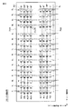
1−3.メモリセルアレイおよび電源電圧発生回路の構成例
次に、図3を用いて、メモリセルアレイ11および電源電圧発生回路19の構成例について説明する。図示するように、メモリセルアレイ11は、本例の場合、4つのプレーン(Plane 0, Plane 1, Plane 2, Plane 3)を備える。
1-3. Configuration example of memory cell array and power supply voltage generation circuit
Next, configuration examples of the
プレーンPL0は、複数のブロック(図示を省略)、センスアンプS0、ブロックデコーダBD0、およびローカルスイッチLSW(HV)を備える。
ブロックの構成の詳細な説明は省略するが、図示するように少なくともワード線方向に沿って複数のワード線WLsが配置される。センスアンプS0は、ビット線方向に複数ブロックを挟むように配置され、メモリセルトランジスタから読み出したデータを読み出す。ブロックデコーダBD0は、ビット線方向に沿ったローカル制御線LGCLを備え、ブロック選択信号に従って、複数のブロックのいずれかを選択する。ローカルスイッチLSWは、制御回路17から入力されるローカル制御信号CSW0に従い、ブロックデコーダBD0のオン/オフを切り替える。
The plane PL0 includes a plurality of blocks (not shown), a sense amplifier S0, a block decoder BD0, and a local switch LSW (HV).
Although a detailed description of the block configuration is omitted, a plurality of word lines WLs are arranged along at least the word line direction as shown. The sense amplifier S0 is arranged so as to sandwich a plurality of blocks in the bit line direction, and reads data read from the memory cell transistor. The block decoder BD0 includes a local control line LGCL along the bit line direction, and selects one of the plurality of blocks according to the block selection signal. The local switch LSW switches on / off the block decoder BD0 in accordance with the local control signal CSW0 input from the
その他のプレーンPL1〜PL3の構成については、上記プレーンPL0と実質的に同様であるので、詳細な説明を省略する。 Since the configurations of the other planes PL1 to PL3 are substantially the same as the plane PL0, detailed description thereof is omitted.
電源電圧発生回路19は、グローバルスイッチ回路GSW、共通電圧発生回路HV−C、および複数の電圧発生回路HV−0〜HV−3を備える。
The power supply
グローバルスイッチ回路GSWは、選択されたプレーン(PL0〜PL3)に、共通電圧発生回路HV−Cおよび複数の電圧発生回路HV−0〜HV−3から供給される電源電圧を切り替えて接続する。グローバルスイッチ回路GSWと、複数のプレーン(PL0〜PL3)との間は、グローバルコントロールゲート線GCGLにより電気的に接続される。 The global switch circuit GSW switches and connects the power supply voltages supplied from the common voltage generation circuit HV-C and the plurality of voltage generation circuits HV-0 to HV-3 to the selected planes (PL0 to PL3). The global switch circuit GSW and a plurality of planes (PL0 to PL3) are electrically connected by a global control gate line GCGL.
共通電圧発生回路(HV-Pump)HV−Cは、複数のプレーン(PL0〜PL3)の数によらず一定の供給能力を保って、共通の電源電圧を発生させる。また、共通電圧発生回路HV−Cは、NAND型フラッシュメモリチップがスタンドバイ時は非活性状態となる。 The common voltage generation circuit (HV-Pump) HV-C generates a common power supply voltage while maintaining a constant supply capability regardless of the number of planes (PL0 to PL3). The common voltage generation circuit HV-C is inactive when the NAND flash memory chip is in the standby state.
電圧発生回路(HV-Pump for Plane0〜HV-Pump for Plane3)HV−0〜HV−3は、上記複数のプレーン(PL0〜PL3)の数(本例では、4つ)に対応して配置され、制御回路17より入力される制御信号(Activation Control w/ plane address)PA0〜PA3により選択され、活性化される。選択された電圧発生回路(HV−0〜HV−3)は、各選択プレーン(PL0〜PL3)の配線負荷容量の充電に対して最適な各プレーン用の電源電圧を発生させる。詳細については、後述する。
The voltage generation circuits (HV-Pump for
共通電圧発生回路HV−Cおよび電圧発生回路HV−0〜HV−3と、グローバルスイッチ回路GSWとの間は、ノードN0〜N3を介して、ポンプ部配線PumpLにより電気的に接続される。 The common voltage generation circuit HV-C and the voltage generation circuits HV-0 to HV-3 and the global switch circuit GSW are electrically connected to each other by pump section wiring PumpL via nodes N0 to N3.
1−4.配線構成例
次に、図4を用いて、本例に係る電源電圧発生回路19が充電する配線構成例について説明する。
図示するように、本例に係る電源電圧発生回路19が充電する配線構成は、共通配線部21、ローカル配線部22、およびワード線部23である。
1-4. Wiring configuration example
Next, a wiring configuration example charged by the power supply
As shown in the figure, the wiring configuration charged by the power supply
共通配線部21は、図中の”太線”で示すように、ポンプ部配線PumpLおよびグローバルコントロールゲート線GCGLである。ポンプ部配線PumpLは、共通電圧発生回路HV−Cおよび電圧発生回路HV−0〜HV−3と、グローバルスイッチ回路GSWとの間を電気的に接続する。また、グローバルスイッチ回路GSWは、複数のスイッチング回路SWとスイッチングトランジスタGSTrを備える。スイッチングトランジスタGSTrの電流経路の一端はポンプ部配線PumpLに接続され、電流経路の他端はグローバルコントロールゲート線GCGLに接続され、ゲートから入力されるスイッチング回路SWの出力信号により電流経路のオン/オフが切り替えられる。グローバルコントロールゲート線GCGLは、グローバルスイッチ回路GSWと、ローカルスイッチ回路HVとの間を電気的に接続する。 The common wiring portion 21 is a pump portion wiring PumpL and a global control gate line GCGL as indicated by a “thick line” in the drawing. The pump part wiring PumpL electrically connects the common voltage generation circuit HV-C and the voltage generation circuits HV-0 to HV-3 and the global switch circuit GSW. The global switch circuit GSW includes a plurality of switching circuits SW and a switching transistor GSTr. One end of the current path of the switching transistor GSTr is connected to the pump section wiring PumpL, the other end of the current path is connected to the global control gate line GCGL, and the current path is turned on / off by the output signal of the switching circuit SW input from the gate. Is switched. The global control gate line GCGL electrically connects the global switch circuit GSW and the local switch circuit HV.
ローカル配線部22は、図中の”細線”で示すように、ローカルスイッチ回路HVと、ブロックデコーダスイッチ回路BDSWとの間を電気的に接続する。また、ローカルスイッチ回路HVは、複数のスイッチング回路SWとスイッチングトランジスタLSTrを備える。スイッチングトランジスタLSTrの電流経路の一端はグローバルコントロールゲート線GCGLに接続され、電流経路の他端はブロックデコーダスイッチ回路BDSWに接続され、ゲートから入力されるスイッチング回路SWの出力信号により電流経路のオン/オフが切り替えられる。
The
ワード線部23は、図中の”細線”で示すように、ブロックデコーダスイッチ回路BDSWと、プレーン(Plane 0 〜 Plane 3)との間を電気的に接続する。また、ブロックデコーダスイッチ回路BDSWは、ブロックデコーダ(BD0〜BD3)内に配置され、複数のスイッチング回路SWとスイッチングトランジスタBSTrを備える。スイッチングトランジスタBSTrの電流経路の一端はローカルコントロールゲート線LCGLに接続され、電流経路の他端はワード線WLxに接続され、ゲートから入力されるスイッチング回路SWの出力信号により電流経路のオン/オフが切り替えられる。
The
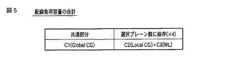
1−5.配線負荷容量の合計
次に、図5を用いて、本例に係る電源電圧発生回路19が充電する配線負荷容量の合計について説明する。上記のように、本例に係るNAND型フラッシュメモリは、メモリセルアレイ11が4分割された4つのプレーン(PL0〜PL3)からなる構成である。
1-5. Total wiring load capacity
Next, the total wiring load capacitance charged by the power supply
ここで、図示するように、電源電圧発生回路19が充電する配線負荷容量の合計は、以下に示す共通部分の負荷容量C1と、選択プレーン数に依存する部分の負荷容量(C2+C3)×4との合計である。即ち、図4中の配線構成において以下のようにそれぞれ対応する。
Here, as shown in the figure, the total of the wiring load capacitance charged by the power supply
共通部分C1:共通配線部分21(図4中の”太線”)の負荷容量
選択プレーン数に依存する部分(C2+C3):ローカル配線部22およびワード線部23(図4中の”細線”)の負荷容量
このように、電源電圧発生回路19が充電する配線負荷容量は、プレーンの選択数に依存せずにグローバルスイッチ回路GSWがオンすると共通に見える負荷容量C1と、複数のプレーン(PL0〜PL3)対応した選択プレーン数に依存する部分(C2+C3)とから構成されることが分かる。
Common part C1: Load capacity of common wiring part 21 ("thick line" in FIG. 4) Part depending on the number of selected planes (C2 + C3):
1−6.選択プレーン数と負荷容量との関係
次に、図6を用いて、本例に係る選択プレーン数と負荷容量との関係について説明する。
図中の中欄(1WL/Plane当たり容量)に示すように、2プレーン以上の複数プレーンを有する半導体集積回路装置では、1プレーン選択時と2プレーン以上の複数のプレーンを同時に選択した際で充電すべき負荷容量が変動する。ここで、本例では、各配線の容量は配線長やトランジスタ数を考慮し、ワード線については2pF程度、ローカルコントロールゲート線については6pF程度、グローバルコントロールゲート線GCGLについては5pF程度、として試算した。
1-6. Relationship between number of selected planes and load capacity
Next, the relationship between the number of selected planes and the load capacity according to this example will be described with reference to FIG.
As shown in the middle column of the figure (capacity per 1 WL / plane), in a semiconductor integrated circuit device having two or more planes, charging is performed when one plane is selected and when two or more planes are simultaneously selected. The load capacity to be changed varies. Here, in this example, the capacitance of each wiring is estimated by considering the wiring length and the number of transistors, and is about 2 pF for the word line, about 6 pF for the local control gate line, and about 5 pF for the global control gate line GCGL. .
結果、本例に係る4プレーン構成では、以下のように変動する。
1Plane選択の場合:5+(2+6)×1=13pF程度
2Plane選択の場合:5+(2+6)×2=21pF程度
3Plane選択の場合:5+(2+6)×3=29pF程度
4Plane選択の場合:5+(2+6)×4=37pF程度
上記のように、負荷容量が選択プレーン数により変動すると、それに伴い充電時間も大きく変化してしまい、動作マージンの悪化を引き起こす原因となる。そのため、選択プレーン数に応じて、電源電圧発生回路の能力を可変とすれば良いとも思われる。
As a result, the 4-plane configuration according to this example varies as follows.
For 1 plane selection: 5+ (2 + 6) × 1 = about 13 pF For 2 plane selection: 5+ (2 + 6) × 2 = about 21 pF For 3 plane selection: 5+ (2 + 6) × 3 = about 29 pF For 4 plane selection: 5+ (2 + 6 ) × 4 = about 37 pF As described above, when the load capacitance fluctuates depending on the number of selected planes, the charging time greatly changes accordingly, causing a deterioration in the operation margin. For this reason, it is considered that the power supply voltage generation circuit may have a variable capacity depending on the number of selected planes.
しかしながら、選択プレーン数により変化する負荷容量に応じて、的確に電源電圧発生回路の供給能力を変化させる制御は容易ではない。 However, it is not easy to control to change the supply capability of the power supply voltage generation circuit accurately according to the load capacity that changes depending on the number of selected planes.
それは、上記図6に示す本例の試算のように、4プレーン構成の半導体集積回路装置の場合、1プレーン動作時と、2プレーン動作、さらに4プレーン同時動作での負荷容量は、単純に1プレーン動作時に比べ2倍、4倍と増加するわけではないからである。 This is because, in the case of a semiconductor integrated circuit device having a 4-plane configuration, as shown in the trial calculation of this example shown in FIG. 6, the load capacity at the time of 1-plane operation, 2-plane operation, and 4-plane simultaneous operation is simply 1. This is because it does not increase by 2 or 4 times compared to the plane operation.
図示するように、1プレーン動作時と2プレーン動作では、2倍にはなっていないことは明らかである。本試算では、選択プレーン数が、2倍、4倍になっても、負荷容量としては、それぞれ1.6倍程度、2.8倍程度となっている。 As shown in the figure, it is clear that the number of times is not doubled in the 1-plane operation and the 2-plane operation. In this trial calculation, even if the number of selected planes is doubled or quadrupled, the load capacity is about 1.6 times or about 2.8 times, respectively.
これは、選択プレーン数に依らず共通部分の負荷容量C1が存在するためである。本例では、グローバルコントロール配線の容量5pF程度に相当する。 This is because there is a common load capacitance C1 regardless of the number of selected planes. In this example, it corresponds to a capacitance of about 5 pF of global control wiring.
ここで、その対応案として、プレーンごとに電圧発生器を設け、当該プレーンが選択された場合のみその電圧発生器を動作させる構成が良いとも思われる。しかしながら、この構成では、2プレーン、4プレーン動作時では、電圧発生器の能力がそれぞれ2倍、4倍となってしまい、実際の負荷容量変化と合致せず、さらに、実際の負荷容量変化に比べ、複数プレーン選択時では過大な能力となってしまう。さらにこの構成では、選択プレーン数によるワード線立上り速度のばらつきによる動作マージンの低下、加えて負荷に比べ過大な能力の電圧発生器が必要となりレイアウト面積の増大ならびに消費電流の増大も懸念される。 Here, as a countermeasure, it may be preferable to provide a voltage generator for each plane, and operate the voltage generator only when the plane is selected. However, in this configuration, the capacity of the voltage generator is doubled and quadrupled when operating in 2 planes and 4 planes, respectively, and does not match the actual load capacity change. In comparison, when multiple planes are selected, the capacity becomes excessive. Further, with this configuration, the operation margin is reduced due to variations in the word line rising speed depending on the number of selected planes. In addition, a voltage generator having an excessive capacity compared with the load is required, which may increase the layout area and the current consumption.
そこで、本例では、複数のプレーン(PL0〜PL3)の数によらず一定の供給能力を保つ共通電圧発生回路HV−Cと、複数のプレーン(PL0〜PL3)の数に対応して配置される複数の電圧発生回路(HV−0〜HV−3)と、を備える電源電圧発生回路19を提案する。 Therefore, in this example, the common voltage generation circuit HV-C that maintains a constant supply capability regardless of the number of the plurality of planes (PL0 to PL3) and the number of the plurality of planes (PL0 to PL3) are arranged. And a plurality of voltage generation circuits (HV-0 to HV-3).
共通電圧発生回路HV−Cは、複数のプレーン(PL0〜PL3)の数によらない共通部分の負荷容量C1を充電する。一方、複数の電圧発生回路(HV−0〜HV−3)は、選択プレーン数に依存する部分の負荷容量(C2+C3)を充電する。 The common voltage generation circuit HV-C charges the load capacitance C1 of the common part regardless of the number of the plurality of planes (PL0 to PL3). On the other hand, the plurality of voltage generation circuits (HV-0 to HV-3) charge a portion of the load capacitance (C2 + C3) depending on the number of selected planes.
例えば、データ読み出し動作時およびデータ読み出し動作時において、1プレーン選択(ここでは、プレーンPL0を選択する)される場合、共通部分のグローバルスイッチ回路GSWに加え、プレーンPL0のローカルスイッチ回路HVおよびブロックデコーダ(ワード線)スイッチ回路BDSWがオン状態となる。 For example, when one plane is selected (in this case, the plane PL0 is selected) in the data read operation and the data read operation, the local switch circuit HV and the block decoder of the plane PL0 are added to the global switch circuit GSW of the common part. The (word line) switch circuit BDSW is turned on.
この場合、電源電圧発生回路19が充電すべき容量は、共通部分の負荷容量C1と、選択プレーン(PL0)数に対応する部分の負荷容量(C2+C3)との和である。即ち、グローバルCG線の容量+プレーンPL0に対応する(ローカルCG線容量+ワード線容量)となる。この際、動作する電源電圧発生回路は、共通電圧発生回路HV−Cと、プレーンPL0用のポンプ回路である1つの電圧発生回路HV−0となる。
In this case, the capacity to be charged by the power supply
次に、例えば、データ読み出し動作時およびデータ読み出し動作時において、4プレーン選択(プレーンPL0〜PL3を選択する)される場合では、電源電圧発生回路19が充電すべき負荷容量は、共通部分の負荷容量C1と、選択プレーン(PL0)数に対応する部分の負荷容量(C2+C3)の4倍との和である。即ち、グローバルCG線の容量+(ローカルCG線容量+ワード線容量)×4倍となる。この際、動作する電源電圧発生回路は、共通電圧発生回路HV−Cと、プレーンPL0〜PL3用の4つの電圧発生回路HV−0〜HV−3となる。
Next, for example, when four planes are selected (planes PL0 to PL3 are selected) during the data read operation and the data read operation, the load capacity to be charged by the power supply
このように、共通電圧発生回路HV−Cを備えることによって、選択プレーン数の変化による負荷変動があった場合であっても、常に最適な制御が容易に可能となる。そのため、2プレーン以上の複数プレーン化が進行し、選択プレーン数の変化に伴って容量負荷が変動した場合であっても、充電時間が選択プレーン数により変動することを防止することができる。そのため、動作マージンを向上することができる。 As described above, by providing the common voltage generation circuit HV-C, even when there is a load variation due to a change in the number of selected planes, optimal control can always be easily performed. Therefore, even when the number of planes of two or more planes advances and the capacity load fluctuates as the number of selected planes changes, it is possible to prevent the charging time from fluctuating depending on the number of selected planes. Therefore, the operation margin can be improved.
加えて、プレーン用の4つの各電圧発生回路HV−0〜HV−3は、全て同じ電圧供給能力であって同一の構成のものを利用することができる。そのため、その制御が非常に容易であるばかりでなく、レイアウト作業量も大幅に低減することが可能である点で、開発期間の短縮化に対しても有利である。 In addition, the four voltage generating circuits HV-0 to HV-3 for the plane can all use the same voltage supply capability and the same configuration. Therefore, not only the control is very easy, but also the layout work amount can be greatly reduced, which is advantageous for shortening the development period.
<2.立ち上がり電圧特性>
次に、図7および図8を用いて、半導体集積回路装置の立ち上がり電圧特性について説明する。
2−1.第1の実施形態に係る立ち上がり速度
まず、図7を用いて、第1の実施形態に係る半導体集積回路装置の立ち上がり電圧特性について説明する。
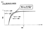
図示するように、時間(time)と電圧(V)との関係に関し、1プレーン選択、2プレーン選択、3プレーン選択、4プレーン選択、のいずれの場合であっても、ほぼ一定の立ち上がり特性を実現している。例えば、本例の場合では、1〜4プレーン選択にかかわらず、ほぼ一定の時間tcの際には、負荷容量を充電できる。
<2. Rising voltage characteristics>
Next, the rising voltage characteristics of the semiconductor integrated circuit device will be described with reference to FIGS.
2-1. Rise speed according to the first embodiment
First, the rising voltage characteristics of the semiconductor integrated circuit device according to the first embodiment will be described with reference to FIG.
As shown in the figure, with respect to the relationship between time (time) and voltage (V), the rise characteristics are almost constant regardless of whether one plane is selected, two planes are selected, three planes are selected, or four planes are selected. Realized. For example, in the case of this example, the load capacity can be charged at a substantially constant time tc regardless of the selection of 1 to 4 planes.
そのため、本例の構成によれば、選択プレーン数に依存せず、ほぼ一定の立ち上がり特性を有することが分かる。 Therefore, according to the configuration of the present example, it can be seen that it has a substantially constant rising characteristic regardless of the number of selected planes.
2−2.比較例に係る立ち上がり速度
続いて、図8を用いて、後述する比較例に係る半導体集積回路装置の立ち上がり電圧特性について説明する。
図示するように、時間(time)と電圧(V)との関係に関し、1プレーン選択、2プレーン選択、3プレーン選択、4プレーン選択、のそれぞれの場合に対し、立ち上がり特性が大きく変動している。例えば、比較例の場合では、順次、1〜4プレーン選択と選択数が増大するに従い、負荷容量の充電時間も増大(時間t1→時間t2、…)する。
2-2. Rise speed according to comparative example
Next, a rising voltage characteristic of a semiconductor integrated circuit device according to a comparative example to be described later will be described with reference to FIG.
As shown in the figure, with respect to the relationship between time (time) and voltage (V), the rising characteristics vary greatly for each of the cases of 1 plane selection, 2 plane selection, 3 plane selection, and 4 plane selection. . For example, in the case of the comparative example, as the 1st to 4th plane selection and the number of selections increase, the load capacity charging time also increases (time t1 → time t2,.
そのため、比較例の構成では、選択プレーン数により、立ち上がり特性が大きく変動することが分かる。 For this reason, in the configuration of the comparative example, it can be seen that the rising characteristic varies greatly depending on the number of selected planes.
<3.作用効果>
第1の実施形態に係る半導体集積回路装置によれば、少なくとも下記(1)乃至(3)の効果が得られる。
<3. Effect>
According to the semiconductor integrated circuit device of the first embodiment, at least the following effects (1) to (3) can be obtained.
(1)動作マージンを向上できる。
上記のように、第1の実施形態に係る半導体集積回路装置は、それぞれが複数のメモリセルMTを有する複数のプレーンPL0〜PL3を備えるメモリセルアレイ11と、一定の供給能力を保つ共通電圧発生回路HV−Cと、複数のプレーンの数に対応して配置される複数の電圧発生回路HV−0〜HV−3とを備える電源電圧発生回路19と、電源電圧発生回路19を制御する制御回路17とを具備する。
(1) The operation margin can be improved.
As described above, the semiconductor integrated circuit device according to the first embodiment includes a
共通電圧発生回路HV−Cは、複数のプレーン(PL0〜PL3)の数によらない共通部分の負荷容量C1を充電する。一方、複数の電圧発生回路(HV−0〜HV−3)は、選択プレーン数に依存する部分の負荷容量(C2+C3)を充電する。 The common voltage generation circuit HV-C charges the load capacitance C1 of the common part regardless of the number of the plurality of planes (PL0 to PL3). On the other hand, the plurality of voltage generation circuits (HV-0 to HV-3) charge a portion of the load capacitance (C2 + C3) depending on the number of selected planes.
例えば、データ読み出し動作時およびデータ読み出し動作時において、1プレーン選択(ここでは、プレーンPL0を選択する)する場合、電源電圧発生回路19が充電すべき容量は、共通部分の負荷容量C1と、選択プレーン(PL0)数に対応する部分の負荷容量(C2+C3)との和である。即ち、グローバルCG線の容量+プレーンPL0に対応する(ローカルCG線容量+ワード線容量)となる。この際、動作する電源電圧発生回路は、共通電圧発生回路HV−Cと、プレーンPL0用のポンプ回路である1つの電圧発生回路HV−0となる。
For example, when one plane is selected (in this case, the plane PL0 is selected) during the data read operation and the data read operation, the capacity to be charged by the power supply
次に、例えば、データ読み出し動作時およびデータ読み出し動作時において、4プレーン選択(プレーンPL0〜PL3を選択する)する場合では、電源電圧発生回路19が充電すべき負荷容量は、共通部分の負荷容量C1と、選択プレーン(PL0)数に対応する部分の負荷容量(C2+C3)の4倍との和である。即ち、グローバルCG線の容量+(ローカルCG線容量+ワード線容量)×4倍となる。この際、動作する電源電圧発生回路は、共通電圧発生回路HV−Cと、プレーンPL0〜PL3用の4つの電圧発生回路HV−0〜HV−3となる。
Next, for example, when selecting four planes (selecting planes PL0 to PL3) during the data read operation and the data read operation, the load capacitance to be charged by the power supply
このように、複数プレーン化の進行に伴って、選択プレーン数の変化による負荷変動があった場合であっても、常に最適な制御が容易に可能となる。そのため、選択プレーン数の変化に伴って容量負荷が変動した場合であっても、充電時間が選択プレーン数により変動することを防止することができる。そのため、動作マージンを向上することができる。 Thus, even when there is a load variation due to a change in the number of selected planes as the number of planes progresses, optimal control can always be easily performed. Therefore, even when the capacity load varies with the change in the number of selected planes, it is possible to prevent the charging time from varying with the number of selected planes. Therefore, the operation margin can be improved.
これは、上述した図7に示した、本願の発明者が得た知見に係る半導体集積回路装置の立ち上がり電圧特性からも明らかである。 This is also apparent from the rising voltage characteristics of the semiconductor integrated circuit device according to the knowledge obtained by the inventors of the present application shown in FIG.
(2)開発期間の短縮化に対して有利である。
加えて、プレーン用の4つの各電圧発生回路HV−0〜HV−3は、全て同じ電圧供給能力であって同一の構成のものを利用することができる。そのため、その制御が非常に容易であるばかりでなく、レイアウト作業量も大幅に低減することが可能である点で、開発期間の短縮化に対して有利である。
(2) It is advantageous for shortening the development period.
In addition, the four voltage generating circuits HV-0 to HV-3 for the plane can all use the same voltage supply capability and the same configuration. Therefore, not only the control is very easy, but also the layout work amount can be greatly reduced, which is advantageous for shortening the development period.
(3)大容量化に対して有利である。
ここで、大容量化を実現するためには、メモリセルの微細化を推し進めつつ、メモリセルアレイを複数プレーン(Plane)化することが有望であると考えられている。
(3) It is advantageous for large capacity.
Here, in order to realize a large capacity, it is considered promising to make a memory cell array into a plurality of planes while promoting miniaturization of memory cells.
本例では、上記(1)での説明のように、動作マージンを悪化することなく、複数プレーン化することができる。そのため、大容量化に対して有利である。また、本例に係る構成は、メモリセルのシュリンクが進んだ、例えば、30nm世代、20nm世代等に対して有望であると予想される。 In this example, as described in the above (1), a plurality of planes can be formed without deteriorating the operation margin. Therefore, it is advantageous for increasing the capacity. Further, the configuration according to this example is expected to be promising for the 30 nm generation, the 20 nm generation, and the like in which the shrinkage of the memory cell has advanced.
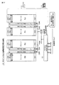
[第2の実施形態(ウェル電圧を選択プレーン数に従って制御する一例)]
次に、第2の実施形態に係る半導体集積回路装置について、図9を用いて説明する。この実施形態は、更にウェル電圧を選択プレーン数に従って制御する一例に関するものである。この説明において、上記第1の実施形態と重複する部分の詳細な説明を省略する。
[Second Embodiment (an example in which the well voltage is controlled according to the number of selected planes)]
Next, a semiconductor integrated circuit device according to a second embodiment will be described with reference to FIG. This embodiment further relates to an example in which the well voltage is controlled according to the number of selected planes. In this description, detailed description of the same parts as those in the first embodiment is omitted.
<構成例>
図示するように、第2の実施形態に係る半導体集積回路装置は、下記の点で上記第1の実施形態と相違する。
メモリセルアレイ11に関しては、プレーンPL0〜PL3の両端にブロックデコーダBDおよびローカルスイッチ回路HVがそれぞれ更に配置される。そのため、メモリセルの微細化が進展しても、ブロックデコーダBD0〜BD3のリソグラフィのマージンを拡大できる点で有効である。より具体的には、例えば、1プレーンが2000ブロック程度で構成されている場合、ブロックデコーダBD0〜BD3は、同じ数の2000個を配置する必要がある。ここで、プレーンの片側にのみに配置した場合、片側に2000個のブロックデコーダを、ブロックと同じピッチで配置する必要ある。一方、本例のように、ブロックデコーダBD0〜BD3をプレーンプレーンPL0〜PL3の両側に配置する構成であれば、プレーンの片側に、例えば、1000個ずつ配置すればよい。そのため、ブロックデコーダBD0〜BD3を、ブロックのピッチの2倍で配置できるため、リソグラフィのマージンを向上することができる。
<Configuration example>
As shown in the figure, the semiconductor integrated circuit device according to the second embodiment is different from the first embodiment in the following points.
Regarding
電源電圧発生回路19に関しては、ウェル電圧をプレーンごとに独立に制御し消去動作の際の消去電圧の立ち上がり電圧を一定化するために、消去切り替えスイッチ回路29−1〜29−3と消去電圧モニタ回路MONとを更に備える。
With respect to the power supply
消去電圧モニタ回路MONは、データ消去動作の際に、制御回路17からの制御信号により、共通ノードN0〜N3の出力を複数の消去切り替えスイッチ回路29−0〜29−3に切り替える。
The erase voltage monitor circuit MON switches the outputs of the common nodes N0 to N3 to a plurality of erase changeover switch circuits 29-0 to 29-3 by a control signal from the
消去切り替えスイッチ回路29−1〜29−3は、電流経路の一端が共通電圧発生回路HV−Cの出力および複数の電圧発生回路複数HV−0〜HV−3の出力に接続される共通ノードN0〜N3に接続され、電流経路の他端が複数のプレーンの消去電圧が与えられるウェルWELL<0>〜WELL<3>に接続される。 In the erasure changeover switch circuits 29-1 to 29-3, one end of the current path is connected to the output of the common voltage generation circuit HV-C and the common node N0 connected to the outputs of the plurality of voltage generation circuits HV-0 to HV-3. To N3, and the other end of the current path is connected to wells WELL <0> to WELL <3> to which erase voltages of a plurality of planes are applied.
消去切り替えスイッチ回路29−1〜29−3は、ローカルポンプ回路(LP0〜LP3)およびスイッチングトランジスタ(LPTr0〜LPTr3)を備える。
ローカルポンプ回路LP0は、制御回路17からのウェル制御信号PAW0(enable/disable)に従い、スイッチングトランジスタLPTr0の電流経路の導通/非導通を制御する。その他のローカルポンプ回路LP1〜LP3についても、実質的に同様である。
スイッチングトランジスタLPTr0の電流経路の一端は消去電圧バスノード(VERA bus node)N0に接続され、電流経路の他端はプレーンPL0の消去動作の際に消去電圧VERAが与えられる半導体基板中のウェルWELL<0>に接続され、ゲートはローカルポンプ回路LP0の出力に接続される。その他のスイッチングトランジスタLPTr1〜LPTr3についても、実質的に同様である。
ここで、消去電圧バスノード(VERA bus node)N0〜N3は、上記第1の実施形態に係る図3中の各ノードN0〜N3と共通に用いられる(commonly used)。そのため、各ノードN0〜N3を介して第1の実施形態に係るグローバルスイッチ回路GSWと電気的に接続される構成であっても良い。
The erase changeover switch circuits 29-1 to 29-3 include a local pump circuit (LP0 to LP3) and a switching transistor (LPTr0 to LPTr3).
The local pump circuit LP0 controls conduction / non-conduction of the current path of the switching transistor LPTr0 according to the well control signal PAW0 (enable / disable) from the
One end of the current path of the switching transistor LPTr0 is connected to an erase voltage bus node (VERA bus node) N0, and the other end of the current path is a well WELL <0 in the semiconductor substrate to which the erase voltage VERA is applied in the erase operation of the plane PL0. The gate is connected to the output of the local pump circuit LP0. The same applies to the other switching transistors LPTr1 to LPTr3.
Here, erase voltage bus nodes (VERA bus nodes) N0 to N3 are commonly used with the nodes N0 to N3 in FIG. 3 according to the first embodiment. Therefore, it may be configured to be electrically connected to the global switch circuit GSW according to the first embodiment via the nodes N0 to N3.
本例に係るウェル電圧を与える際の切り替えは、制御回路17からの制御に従った消去電圧モニタ回路MONが行う。
Switching when applying the well voltage according to this example is performed by the erase voltage monitor circuit MON according to the control from the
<データ消去動作(ウェル電圧印加動作)>
次に、第2の実施形態に係る半導体集積回路装置のデータ消去動作(ウェル電圧印加動作)について説明する。
<Data erase operation (well voltage application operation)>
Next, a data erasing operation (well voltage applying operation) of the semiconductor integrated circuit device according to the second embodiment will be described.
ここで、NAND型フラッシュメモリにおいて、メモリセルMTのデータを消去する際には、メモリセルMTが形成される半導体基板のウェル側に高電圧の消去電圧(VERA)を印加し、電化蓄積層FGから電子を引き抜くことにより行う。本例のような複数プレーンの場合、ウェルの負荷容量は非常に大きいので、消去すべきブロックが存在するプレーンのウェルのみ高電圧を印加することが望ましい。 Here, in the NAND flash memory, when erasing data in the memory cell MT, a high erasing voltage (VERA) is applied to the well side of the semiconductor substrate in which the memory cell MT is formed, and the charge accumulation layer FG is applied. This is done by extracting electrons from In the case of a plurality of planes as in this example, since the load capacity of the well is very large, it is desirable to apply a high voltage only to the well of the plane where the block to be erased exists.
しかしながら、消去電圧をプレーンごとの独立制御にした場合にも、1プレーン時の消去と2プレーン時の消去、さらには4プレーン時の消去で消去電圧の立ち上がりが大きく異なると、選択プレーン数により実効的な消去電圧印加時間が大きくばらつき、消去特性が大きく異なる原因となる。そのため、選択プレーン数に係らず同じ様に充電速度を調節できることが望ましい。さらに、1プレーン時も4プレーンと同じ電源電圧発生回路では、能力が過大となるとともに消費電流も大きくなってしまい好ましくない。 However, even if the erase voltage is controlled independently for each plane, if the rise of the erase voltage differs greatly between the erase for one plane and the erase for two planes, and even the erase for four planes, it will be effective depending on the number of selected planes. The erasing voltage application time varies widely and causes the erasing characteristics to vary greatly. Therefore, it is desirable that the charging rate can be adjusted in the same manner regardless of the number of selected planes. Further, even in the case of one plane, the same power supply voltage generation circuit as that in the four planes is not preferable because the capacity becomes excessive and the current consumption increases.
そこで、第2の実施形態では、上記共通電源電圧回路HV−Cとプレーン数と同数のプレーン用の複数の電源電圧発生回路HV−0〜HV−3から構成される上記電源電圧発生回路19を、データ消去動作の際にも適用する。
Therefore, in the second embodiment, the power supply
より具体的には、制御回路17より電源電圧発生回路HV−0〜HV−3に、消去制御信号(Control Signals (inc.DAC))が共通に入力されると、消去電圧モニタ回路MONが、消去電圧バスノードN0〜N3の電流経路をウェル側に切り替えることによって、データ消去動作に移行する。
More specifically, when an erase control signal (Control Signals (inc. DAC)) is commonly input from the
続いて、第1の実施形態と同様に、制御回路17より制御信号PA0〜PA3、PAW0〜PAW3が、電圧発生回路HV−0〜HV−3およびローカルポンプ回路LP0〜LP3に入力されることにより、上記第1の実施形態と同様に、選択されたプレーンのウェル(WELL<0>〜WELL<3>)にウェル電圧を与える。
Subsequently, as in the first embodiment, control signals PA0 to PA3 and PAW0 to PAW3 are input from the
そのため、データ消去動作の際に、選択プレーン数が変化しても常にほぼ同様な充電速度に保つことが可能となる。 For this reason, during the data erasing operation, it is possible to always maintain substantially the same charging speed even if the number of selected planes changes.
<作用効果>
第2の実施形態に係る半導体集積回路装置によれば、少なくとも上記(1)乃至(3)と同様の効果が得られる。さらに、下記(4)の効果が得られる。
<Effect>
According to the semiconductor integrated circuit device of the second embodiment, at least the same effects as the above (1) to (3) can be obtained. Furthermore, the following effect (4) can be obtained.
(4)データ動作の際にも、動作マージンを向上できる。
さらに、第2の実施形態に係る半導体集積回路装置は、電源電圧発生回路19に関し、ローカルポンプ回路(LP0〜LP3)、スイッチングトランジスタ(LPTr0〜LPTr3)、および消去電圧モニタ回路MONを更に備える。
そのため、制御回路17より電源電圧発生回路HV−0〜HV−3に、消去制御信号(Control Signals (inc.DAC))が共通に入力されると、消去電圧モニタ回路MONが消去電圧バスノードN0〜N3の電流経路をウェル側に切り替えることによって、データ消去動作に移行する。
(4) The operation margin can be improved also in the data operation.
The semiconductor integrated circuit device according to the second embodiment further includes a local pump circuit (LP0 to LP3), a switching transistor (LPTr0 to LPTr3), and an erasing voltage monitor circuit MON for the power supply
Therefore, when an erase control signal (Control Signals (inc. DAC)) is commonly input from the
続いて、第1の実施形態と同様に、制御回路17より制御信号PA0〜PA3、PAW0〜PAW3が、電圧発生回路HV−0〜HV−3およびローカルポンプ回路LP0〜LP3に入力されることにより、上記第1の実施形態と同様に、選択されたプレーンのウェル(WELL<0>〜WELL<3>)にウェル電圧を与える。
Subsequently, as in the first embodiment, control signals PA0 to PA3 and PAW0 to PAW3 are input from the
そのため、データ消去動作の際に、選択プレーン数が変化しても常にほぼ同様な充電速度に保つことが可能となる。結果、データ動作の際にも、動作マージンを向上できる。 For this reason, during the data erasing operation, it is possible to always maintain substantially the same charging speed even if the number of selected planes changes. As a result, the operation margin can be improved also in the data operation.
[第3の実施形態]
次に、第3の実施形態に係る半導体集積回路装置について、図10を用いて説明する。この説明において、上記第2の実施形態と重複する部分の詳細な説明を省略する。
[Third Embodiment]
Next, a semiconductor integrated circuit device according to a third embodiment will be described with reference to FIG. In this description, a detailed description of portions overlapping with those of the second embodiment is omitted.
図示するように、本例に係る半導体集積回路装置は、出力が消去電圧バスノードN0〜N3にそれぞれ接続される消去電圧モニタ回路MON0〜MON3を更に備える点で、上記第2の実施形態と相違する。消去電圧モニタ回路MON0〜MON3は、プレーンPL0〜PL3ごとに所望なウェル電圧を与えるように、制御回路17からの制御に応じて、消去電圧バスノードN0〜N3の消去バスノードN0〜N3を切り替える。
As shown in the figure, the semiconductor integrated circuit device according to this example is different from the second embodiment in that it further includes erase voltage monitor circuits MON0 to MON3 whose outputs are connected to erase voltage bus nodes N0 to N3, respectively. . Erase voltage monitor circuits MON0 to MON3 switch erase bus nodes N0 to N3 of erase voltage bus nodes N0 to N3 in accordance with control from
第3の実施形態に係る半導体集積回路装置によれば、少なくとも上記(1)乃至(4)と同様の効果が得られる。さらに、必要に応じて、本例のような構成を適用することが可能である。 According to the semiconductor integrated circuit device of the third embodiment, at least the same effects as the above (1) to (4) can be obtained. Furthermore, it is possible to apply the configuration as in this example as necessary.
[比較例(プレーン一括制御の一例)]
次に、上記第1乃至第3の実施形態に係る半導体集積回路装置と比較するために、比較例に係る半導体集積回路装置について、図11を用いて説明する。この比較例は、プレーンの電源電圧を一括して制御する一例に関するものである。この説明において、上記第1の実施形態と重複する部分の詳細な説明を省略する。尚、本比較例に係る構成は、出願時における客観的な従来例に係る構成を示すものではなく、上記第1乃至第3の実施形態に係る半導体集積回路装置と比較するための一例である。
[Comparative example (Example of plane batch control)]
Next, for comparison with the semiconductor integrated circuit device according to the first to third embodiments, a semiconductor integrated circuit device according to a comparative example will be described with reference to FIG. This comparative example relates to an example of collectively controlling the power supply voltage of a plane. In this description, detailed description of the same parts as those in the first embodiment is omitted. The configuration according to this comparative example does not show the configuration according to the objective conventional example at the time of filing, but is an example for comparison with the semiconductor integrated circuit device according to the first to third embodiments. .
図示するように、本比較例に係るメモリセルアレイ111が複数のプレーン(PL0〜PL3)を備えている点で、上記第1乃至第3の実施形態と共通する。
As shown in the figure, the
一方、本比較例に係る電源電圧発生回路119は、単一の電圧発生回路HV(HV-Pump for all planes)のみを備え、プレーンの選択数にかかわらず電圧発生回路HVのみにより、電源電圧が与えられる点で、上記第1乃至第3の実施形態と相違する。
On the other hand, the power supply
そのため、本比較例に係る構成では、例えば、データ読み出し動作、データ書き込み動作の際には、選択プレーン数に関係なく、入力されるワード線本数(例えば、4本、8本、16本、…)に係る制御信号により、与えられる電源電圧が制御される。ここで、単一のプレーン構成の場合、この構成および制御であっても、負荷容量の変動による、動作マージンの悪化は発生しない。 Therefore, in the configuration according to this comparative example, for example, in the data read operation and data write operation, the number of input word lines (for example, 4, 8, 16,..., Regardless of the number of selected planes). The power supply voltage to be applied is controlled by the control signal related to (). Here, in the case of a single plane configuration, even with this configuration and control, the operation margin does not deteriorate due to the change in load capacity.
しかしながら、2プレーン以上の複数プレーンを有する半導体集積回路装置では、1プレーン選択時と2プレーン以上の複数のプレーンを同時に選択した際で充電すべき負荷容量が変動する。充電時間が選択プレーン数により大きく変化してしまい動作マージンの悪化を引き起こす原因となる。そのため、選択プレーン数に応じて、電源電圧発生回路の能力を可変とすれば良いとも思われるが、選択プレーン数により変化する負荷容量に応じて、的確に電源電圧発生回路の供給能力を変化させる制御は容易ではない。 However, in a semiconductor integrated circuit device having two or more planes, the load capacity to be charged varies when one plane is selected and when two or more planes are simultaneously selected. Charging time varies greatly depending on the number of selected planes, which causes a deterioration in operation margin. Therefore, it seems that it is sufficient to make the power supply voltage generation circuit capacity variable according to the number of selected planes. However, the supply capacity of the power supply voltage generation circuit is accurately changed according to the load capacity that changes depending on the number of selected planes. Control is not easy.
それは、上記図6に示した試算のように、4プレーン構成の半導体集積回路装置の場合、1プレーン動作時と、2プレーン動作、さらに4プレーン同時動作での負荷容量は、単純に1プレーン動作時に比べ2倍、4倍と増加するわけではないからである。 As shown in the calculation shown in FIG. 6, in the case of a semiconductor integrated circuit device having a 4-plane configuration, the load capacity during 1-plane operation, 2-plane operation, and 4-plane simultaneous operation is simply 1-plane operation. This is because it does not increase by 2 or 4 times compared to the time.
従って、比較例に係る構成では、立ち上がり電圧特性は、上記図8に示したように、順次、1〜4プレーン選択と選択数が増大するに従い、負荷容量の充電時間も増大(時間t1→時間t2、…)する。
Therefore, in the configuration according to the comparative example, as shown in FIG. 8, the rising voltage characteristics increase the charging time of the load capacity (time t1 → time as the number of selected
このように、比較例に係る構成および動作では、プレーン以上の複数プレーン化が進行すると、選択プレーン数の変化に伴って容量負荷が変動するため、充電時間が選択プレーン数により大きく変動する。そのため、動作マージンが低減する点で不利である。また、大容量化に対しても不利であると言える。 As described above, in the configuration and operation according to the comparative example, when the number of planes equal to or greater than that of the plane progresses, the capacity load varies with the change in the number of selected planes. Therefore, it is disadvantageous in that the operation margin is reduced. Moreover, it can be said that it is disadvantageous for large capacity.
以上、第1乃至第3の実施形態および比較例を用いて本発明の説明を行ったが、この発明は上記各実施形態に限定されるものではなく、実施段階ではその要旨を逸脱しない範囲で種々に変形することが可能である。また、上記各実施形態および比較例には種々の段階の発明が含まれており、開示される複数の構成要件の適宜な組み合わせにより種々の発明が抽出され得る。例えば各実施形態および比較例に示される全構成要件からいくつかの構成要件が削除されても、発明が解決しようとする課題の欄で述べた課題の少なくとも1つが解決でき、発明の効果の欄で述べられている効果の少なくとも1つが得られる場合には、この構成要件が削除された構成が発明として抽出され得る。 The present invention has been described above using the first to third embodiments and the comparative example. However, the present invention is not limited to the above-described embodiments, and the scope of the invention is not deviated from the scope of the invention. Various modifications are possible. The above embodiments and comparative examples include inventions at various stages, and various inventions can be extracted by appropriately combining a plurality of disclosed constituent elements. For example, even if some constituent elements are deleted from all the constituent elements shown in the embodiments and comparative examples, at least one of the problems described in the column of problems to be solved by the invention can be solved, and the column of the effect of the invention In the case where at least one of the effects described in (1) is obtained, a configuration in which this configuration requirement is deleted can be extracted as an invention.
11…メモリセルアレイ、HV−C…共通電源電圧発生回路、HV−0〜HV−3…電源電圧発生回路、19…電源電圧発生回路、17…制御回路。
DESCRIPTION OF
Claims (5)
一定の供給能力を保つ共通電圧発生回路と、前記複数のプレーンの数に対応して配置される複数の電圧発生回路とを備える電源電圧発生回路と、
前記電源電圧発生回路を制御する制御回路とを具備すること
を特徴とする半導体集積回路装置。 A memory cell array comprising a plurality of planes each having a plurality of memory cells;
A power supply voltage generation circuit comprising a common voltage generation circuit that maintains a constant supply capability, and a plurality of voltage generation circuits arranged corresponding to the number of the plurality of planes;
A semiconductor integrated circuit device comprising: a control circuit that controls the power supply voltage generation circuit.
前記複数の電圧発生回路は、ローカル配線およびワード線の負荷容量を充電すること
を特徴とする請求項1に記載の半導体集積回路装置。 The common voltage generation circuit charges the load capacity of the common wiring,
The semiconductor integrated circuit device according to claim 1, wherein the plurality of voltage generation circuits charge a load capacitance of a local wiring and a word line.
を特徴とする請求項1または2に記載の半導体集積回路装置。 3. The semiconductor integrated circuit device according to claim 1, wherein the common voltage generation circuit is inactivated when the semiconductor integrated circuit device is in a standby state.
前記制御回路の制御により、前記共通ノードの出力を前記複数の消去切り替えスイッチ回路に切り替える電圧モニタ回路とを更に備えること
を特徴とする請求項1乃至3のいずれか1項に記載の半導体集積回路装置。 The power supply voltage generation circuit has one end of a current path connected to a common node connected to an output of the common voltage generation circuit and an output of the plurality of voltage generation circuits, and the other end of the current path erases the plurality of planes A plurality of changeover switch circuits connected to a well to which a voltage is applied;
4. The semiconductor integrated circuit according to claim 1, further comprising: a voltage monitor circuit that switches an output of the common node to the plurality of erase changeover switch circuits under the control of the control circuit. 5. apparatus.
を特徴とする請求項1乃至3のいずれか1項に記載の半導体集積回路装置。 4. The plurality of planes are configured by a plurality of blocks each having a plurality of memory cells and a plurality of dummy memory cells arranged at intersections of the word lines and bit lines. The semiconductor integrated circuit device according to any one of the above.
Priority Applications (2)
| Application Number | Priority Date | Filing Date | Title |
|---|---|---|---|
| JP2009106671A JP2010257528A (en) | 2009-04-24 | 2009-04-24 | Semiconductor integrated circuit device |
| US12/754,206 US20100271879A1 (en) | 2009-04-24 | 2010-04-05 | Semiconductor integrated circuit device |
Applications Claiming Priority (1)
| Application Number | Priority Date | Filing Date | Title |
|---|---|---|---|
| JP2009106671A JP2010257528A (en) | 2009-04-24 | 2009-04-24 | Semiconductor integrated circuit device |
Publications (1)
| Publication Number | Publication Date |
|---|---|
| JP2010257528A true JP2010257528A (en) | 2010-11-11 |
Family
ID=42991988
Family Applications (1)
| Application Number | Title | Priority Date | Filing Date |
|---|---|---|---|
| JP2009106671A Pending JP2010257528A (en) | 2009-04-24 | 2009-04-24 | Semiconductor integrated circuit device |
Country Status (2)
| Country | Link |
|---|---|
| US (1) | US20100271879A1 (en) |
| JP (1) | JP2010257528A (en) |
Cited By (1)
| Publication number | Priority date | Publication date | Assignee | Title |
|---|---|---|---|---|
| CN113345899A (en) * | 2020-03-03 | 2021-09-03 | 爱思开海力士有限公司 | Memory device and method of operating the same |
Families Citing this family (3)
| Publication number | Priority date | Publication date | Assignee | Title |
|---|---|---|---|---|
| US8947934B2 (en) * | 2011-12-29 | 2015-02-03 | Micron Technology, Inc. | Sharing local control lines across multiple planes in a memory device |
| KR102818380B1 (en) * | 2019-08-13 | 2025-06-10 | 에스케이하이닉스 주식회사 | Semiconductor memory device and opearting method thereof |
| KR20210123528A (en) | 2020-04-03 | 2021-10-14 | 삼성전자주식회사 | Nonvolatile memory device and operation method thereof |
Citations (4)
| Publication number | Priority date | Publication date | Assignee | Title |
|---|---|---|---|---|
| JPH01282796A (en) * | 1988-05-07 | 1989-11-14 | Mitsubishi Electric Corp | Non-volatile semiconductor storage |
| JPH06215568A (en) * | 1992-10-08 | 1994-08-05 | Gold Star Electron Co Ltd | Back-bias-voltage generation circuit of semiconductor memory device |
| JPH11297071A (en) * | 1998-04-10 | 1999-10-29 | Hitachi Ltd | Semiconductor device |
| JP2001325795A (en) * | 1999-05-10 | 2001-11-22 | Toshiba Corp | Semiconductor device |
Family Cites Families (7)
| Publication number | Priority date | Publication date | Assignee | Title |
|---|---|---|---|---|
| US6122219A (en) * | 1998-07-14 | 2000-09-19 | Winbond Electronics Corporation America | Split array semiconductor graphics memory architecture supporting maskable block write operation |
| US6377502B1 (en) * | 1999-05-10 | 2002-04-23 | Kabushiki Kaisha Toshiba | Semiconductor device that enables simultaneous read and write/erase operation |
| JP4707244B2 (en) * | 2000-03-30 | 2011-06-22 | ルネサスエレクトロニクス株式会社 | Semiconductor memory device and semiconductor device |
| JP4005895B2 (en) * | 2002-09-30 | 2007-11-14 | 株式会社東芝 | Nonvolatile semiconductor memory device |
| KR100798797B1 (en) * | 2006-06-30 | 2008-01-29 | 주식회사 하이닉스반도체 | A semiconductor memory device having an internal voltage generator and a driving method thereof |
| KR100764060B1 (en) * | 2006-09-29 | 2007-10-09 | 삼성전자주식회사 | Nonvolatile Memory Device and System and Memory Cell Array Structure for It |
| JP2010257530A (en) * | 2009-04-24 | 2010-11-11 | Toshiba Corp | Semiconductor integrated circuit device |
-
2009
- 2009-04-24 JP JP2009106671A patent/JP2010257528A/en active Pending
-
2010
- 2010-04-05 US US12/754,206 patent/US20100271879A1/en not_active Abandoned
Patent Citations (4)
| Publication number | Priority date | Publication date | Assignee | Title |
|---|---|---|---|---|
| JPH01282796A (en) * | 1988-05-07 | 1989-11-14 | Mitsubishi Electric Corp | Non-volatile semiconductor storage |
| JPH06215568A (en) * | 1992-10-08 | 1994-08-05 | Gold Star Electron Co Ltd | Back-bias-voltage generation circuit of semiconductor memory device |
| JPH11297071A (en) * | 1998-04-10 | 1999-10-29 | Hitachi Ltd | Semiconductor device |
| JP2001325795A (en) * | 1999-05-10 | 2001-11-22 | Toshiba Corp | Semiconductor device |
Cited By (1)
| Publication number | Priority date | Publication date | Assignee | Title |
|---|---|---|---|---|
| CN113345899A (en) * | 2020-03-03 | 2021-09-03 | 爱思开海力士有限公司 | Memory device and method of operating the same |
Also Published As
| Publication number | Publication date |
|---|---|
| US20100271879A1 (en) | 2010-10-28 |
Similar Documents
| Publication | Publication Date | Title |
|---|---|---|
| JP3913952B2 (en) | Semiconductor memory device | |
| JP4907897B2 (en) | Nonvolatile semiconductor memory device | |
| US8325532B2 (en) | Semiconductor integrated circuit device | |
| JP2011014205A (en) | Nonvolatile semiconductor memory | |
| JP5972700B2 (en) | Memory device | |
| JP2003242792A (en) | Nonvolatile semiconductor memory device | |
| US20030021167A1 (en) | Non-volatile semiconductor memory device | |
| JP2008146800A (en) | Erase circuit of nonvolatile semiconductor memory device | |
| JP2010257528A (en) | Semiconductor integrated circuit device | |
| JP2008103643A (en) | Nonvolatile semiconductor memory | |
| JP3998908B2 (en) | Nonvolatile memory device | |
| US6738292B2 (en) | Nonvolatile semiconductor storage device | |
| US8520465B2 (en) | Semiconductor device | |
| JP2011108349A (en) | Semiconductor memory device | |
| JP2008004196A (en) | Semiconductor memory device | |
| US8873312B2 (en) | Decoder circuit of semiconductor storage device | |
| US12027208B2 (en) | Voltage control in semiconductor memory device | |
| KR100875012B1 (en) | Voltage providing circuit, flash memory device comprising same and operating voltage providing method | |
| CN100541667C (en) | Nonvolatile semiconductor memory | |
| JP2008103033A (en) | Semiconductor memory device and power supply method in the same | |
| JP2003016792A (en) | Non-volatile semiconductor memory | |
| KR20070021758A (en) | X-Decoder of NAND Flash Memory and Its Decoder Placement Method | |
| US8331191B2 (en) | Semiconductor integrated circuit device | |
| JP2006085839A (en) | Nonvolatile semiconductor memory device and control method of the same | |
| JP2006065928A (en) | Nonvolatile semiconductor storage device and semiconductor integrated circuit device |
Legal Events
| Date | Code | Title | Description |
|---|---|---|---|
| A621 | Written request for application examination |
Free format text: JAPANESE INTERMEDIATE CODE: A621 Effective date: 20110912 |
|
| A977 | Report on retrieval |
Free format text: JAPANESE INTERMEDIATE CODE: A971007 Effective date: 20121206 |
|
| A131 | Notification of reasons for refusal |
Free format text: JAPANESE INTERMEDIATE CODE: A131 Effective date: 20121211 |
|
| A02 | Decision of refusal |
Free format text: JAPANESE INTERMEDIATE CODE: A02 Effective date: 20130730 |