JP2010245030A - Lighting device - Google Patents
Lighting device Download PDFInfo
- Publication number
- JP2010245030A JP2010245030A JP2010056928A JP2010056928A JP2010245030A JP 2010245030 A JP2010245030 A JP 2010245030A JP 2010056928 A JP2010056928 A JP 2010056928A JP 2010056928 A JP2010056928 A JP 2010056928A JP 2010245030 A JP2010245030 A JP 2010245030A
- Authority
- JP
- Japan
- Prior art keywords
- layer
- lighting device
- light
- electrode layer
- substrate
- Prior art date
- Legal status (The legal status is an assumption and is not a legal conclusion. Google has not performed a legal analysis and makes no representation as to the accuracy of the status listed.)
- Withdrawn
Links
Images


Classifications
-
- H—ELECTRICITY
- H10—SEMICONDUCTOR DEVICES; ELECTRIC SOLID-STATE DEVICES NOT OTHERWISE PROVIDED FOR
- H10K—ORGANIC ELECTRIC SOLID-STATE DEVICES
- H10K50/00—Organic light-emitting devices
- H10K50/10—OLEDs or polymer light-emitting diodes [PLED]
- H10K50/11—OLEDs or polymer light-emitting diodes [PLED] characterised by the electroluminescent [EL] layers
-
- F—MECHANICAL ENGINEERING; LIGHTING; HEATING; WEAPONS; BLASTING
- F21—LIGHTING
- F21S—NON-PORTABLE LIGHTING DEVICES; SYSTEMS THEREOF; VEHICLE LIGHTING DEVICES SPECIALLY ADAPTED FOR VEHICLE EXTERIORS
- F21S41/00—Illuminating devices specially adapted for vehicle exteriors, e.g. headlamps
- F21S41/10—Illuminating devices specially adapted for vehicle exteriors, e.g. headlamps characterised by the light source
- F21S41/14—Illuminating devices specially adapted for vehicle exteriors, e.g. headlamps characterised by the light source characterised by the type of light source
- F21S41/141—Light emitting diodes [LED]
- F21S41/155—Surface emitters, e.g. organic light emitting diodes [OLED]
-
- F—MECHANICAL ENGINEERING; LIGHTING; HEATING; WEAPONS; BLASTING
- F21—LIGHTING
- F21V—FUNCTIONAL FEATURES OR DETAILS OF LIGHTING DEVICES OR SYSTEMS THEREOF; STRUCTURAL COMBINATIONS OF LIGHTING DEVICES WITH OTHER ARTICLES, NOT OTHERWISE PROVIDED FOR
- F21V21/00—Supporting, suspending, or attaching arrangements for lighting devices; Hand grips
- F21V21/002—Supporting, suspending, or attaching arrangements for lighting devices; Hand grips making direct electrical contact, e.g. by piercing
-
- H—ELECTRICITY
- H01—ELECTRIC ELEMENTS
- H01L—SEMICONDUCTOR DEVICES NOT COVERED BY CLASS H10
- H01L33/00—Semiconductor devices with at least one potential-jump barrier or surface barrier specially adapted for light emission; Processes or apparatus specially adapted for the manufacture or treatment thereof or of parts thereof; Details thereof
- H01L33/02—Semiconductor devices with at least one potential-jump barrier or surface barrier specially adapted for light emission; Processes or apparatus specially adapted for the manufacture or treatment thereof or of parts thereof; Details thereof characterised by the semiconductor bodies
-
- H—ELECTRICITY
- H01—ELECTRIC ELEMENTS
- H01L—SEMICONDUCTOR DEVICES NOT COVERED BY CLASS H10
- H01L33/00—Semiconductor devices with at least one potential-jump barrier or surface barrier specially adapted for light emission; Processes or apparatus specially adapted for the manufacture or treatment thereof or of parts thereof; Details thereof
- H01L33/48—Semiconductor devices with at least one potential-jump barrier or surface barrier specially adapted for light emission; Processes or apparatus specially adapted for the manufacture or treatment thereof or of parts thereof; Details thereof characterised by the semiconductor body packages
- H01L33/62—Arrangements for conducting electric current to or from the semiconductor body, e.g. lead-frames, wire-bonds or solder balls
-
- H—ELECTRICITY
- H05—ELECTRIC TECHNIQUES NOT OTHERWISE PROVIDED FOR
- H05B—ELECTRIC HEATING; ELECTRIC LIGHT SOURCES NOT OTHERWISE PROVIDED FOR; CIRCUIT ARRANGEMENTS FOR ELECTRIC LIGHT SOURCES, IN GENERAL
- H05B33/00—Electroluminescent light sources
- H05B33/12—Light sources with substantially two-dimensional radiating surfaces
- H05B33/22—Light sources with substantially two-dimensional radiating surfaces characterised by the chemical or physical composition or the arrangement of auxiliary dielectric or reflective layers
-
- H—ELECTRICITY
- H05—ELECTRIC TECHNIQUES NOT OTHERWISE PROVIDED FOR
- H05B—ELECTRIC HEATING; ELECTRIC LIGHT SOURCES NOT OTHERWISE PROVIDED FOR; CIRCUIT ARRANGEMENTS FOR ELECTRIC LIGHT SOURCES, IN GENERAL
- H05B33/00—Electroluminescent light sources
- H05B33/12—Light sources with substantially two-dimensional radiating surfaces
- H05B33/26—Light sources with substantially two-dimensional radiating surfaces characterised by the composition or arrangement of the conductive material used as an electrode
- H05B33/28—Light sources with substantially two-dimensional radiating surfaces characterised by the composition or arrangement of the conductive material used as an electrode of translucent electrodes
-
- H—ELECTRICITY
- H10—SEMICONDUCTOR DEVICES; ELECTRIC SOLID-STATE DEVICES NOT OTHERWISE PROVIDED FOR
- H10K—ORGANIC ELECTRIC SOLID-STATE DEVICES
- H10K50/00—Organic light-emitting devices
- H10K50/10—OLEDs or polymer light-emitting diodes [PLED]
- H10K50/14—Carrier transporting layers
- H10K50/15—Hole transporting layers
- H10K50/156—Hole transporting layers comprising a multilayered structure
-
- F—MECHANICAL ENGINEERING; LIGHTING; HEATING; WEAPONS; BLASTING
- F21—LIGHTING
- F21K—NON-ELECTRIC LIGHT SOURCES USING LUMINESCENCE; LIGHT SOURCES USING ELECTROCHEMILUMINESCENCE; LIGHT SOURCES USING CHARGES OF COMBUSTIBLE MATERIAL; LIGHT SOURCES USING SEMICONDUCTOR DEVICES AS LIGHT-GENERATING ELEMENTS; LIGHT SOURCES NOT OTHERWISE PROVIDED FOR
- F21K9/00—Light sources using semiconductor devices as light-generating elements, e.g. using light-emitting diodes [LED] or lasers
- F21K9/20—Light sources comprising attachment means
- F21K9/23—Retrofit light sources for lighting devices with a single fitting for each light source, e.g. for substitution of incandescent lamps with bayonet or threaded fittings
-
- F—MECHANICAL ENGINEERING; LIGHTING; HEATING; WEAPONS; BLASTING
- F21—LIGHTING
- F21S—NON-PORTABLE LIGHTING DEVICES; SYSTEMS THEREOF; VEHICLE LIGHTING DEVICES SPECIALLY ADAPTED FOR VEHICLE EXTERIORS
- F21S8/00—Lighting devices intended for fixed installation
- F21S8/03—Lighting devices intended for fixed installation of surface-mounted type
-
- F—MECHANICAL ENGINEERING; LIGHTING; HEATING; WEAPONS; BLASTING
- F21—LIGHTING
- F21S—NON-PORTABLE LIGHTING DEVICES; SYSTEMS THEREOF; VEHICLE LIGHTING DEVICES SPECIALLY ADAPTED FOR VEHICLE EXTERIORS
- F21S8/00—Lighting devices intended for fixed installation
- F21S8/04—Lighting devices intended for fixed installation intended only for mounting on a ceiling or the like overhead structures
-
- F—MECHANICAL ENGINEERING; LIGHTING; HEATING; WEAPONS; BLASTING
- F21—LIGHTING
- F21Y—INDEXING SCHEME ASSOCIATED WITH SUBCLASSES F21K, F21L, F21S and F21V, RELATING TO THE FORM OR THE KIND OF THE LIGHT SOURCES OR OF THE COLOUR OF THE LIGHT EMITTED
- F21Y2105/00—Planar light sources
-
- F—MECHANICAL ENGINEERING; LIGHTING; HEATING; WEAPONS; BLASTING
- F21—LIGHTING
- F21Y—INDEXING SCHEME ASSOCIATED WITH SUBCLASSES F21K, F21L, F21S and F21V, RELATING TO THE FORM OR THE KIND OF THE LIGHT SOURCES OR OF THE COLOUR OF THE LIGHT EMITTED
- F21Y2115/00—Light-generating elements of semiconductor light sources
- F21Y2115/20—Electroluminescent [EL] light sources
Abstract
Description
本発明の一形態は、エレクトロルミネセンスを発現する発光部材を含む照明装置に関する。 One embodiment of the present invention relates to a lighting device including a light-emitting member that exhibits electroluminescence.
白熱電球や蛍光灯よりも発光効率が高いという試算から、次世代の照明器具としてエレクトロルミネセンス材料を用いた照明装置が注目されている。エレクトロルミネセンス材料は蒸着法や塗布法などの製法により厚さ1μm以下の薄膜で形成可能であり、また照明装置としての形態にも工夫が施されている。例えば、エレクトロルミネセンス材料を用いた照明装置を大面積化しても輝度を均一に保つことができる照明装置が開示されている(例えば、特許文献1参照。)。 From the estimation that the luminous efficiency is higher than incandescent bulbs and fluorescent lamps, lighting devices using electroluminescent materials are attracting attention as next-generation lighting fixtures. The electroluminescent material can be formed as a thin film having a thickness of 1 μm or less by a manufacturing method such as a vapor deposition method or a coating method, and a device as a lighting device has been devised. For example, a lighting device that can keep the luminance uniform even when the lighting device using an electroluminescent material is enlarged is disclosed (for example, refer to Patent Document 1).
また、エレクトロルミネセンスパネルの荷重負担を減らすために、エレクトロルミネセンスパネルを環状に形成し中央部に開口部を形成した照明装置が開示されている(例えば、特許文献2参照。)。この照明装置は、エレクトロルミネセンスパネルの電極の端子を中央の開口部の内側まで引き出し、中央部に取付けた支持部材に設けた駆動回路と、引き出された端子とを接続した構造を有している。 Moreover, in order to reduce the load burden of an electroluminescence panel, the illuminating device which formed the electroluminescence panel in cyclic | annular form and formed the opening part in the center part is disclosed (for example, refer patent document 2). This lighting device has a structure in which the terminal of the electrode of the electroluminescence panel is pulled out to the inside of the central opening, and the drive circuit provided on the support member attached to the central portion is connected to the extracted terminal. Yes.
このような構造の照明装置において、エレクトロルミネセンスパネルの薄膜電極の端子を中央の開口部の内側まで引き出すには、金属板や導線などを薄膜電極に半田付け等して取り付ける必要がある。 In the illuminating device having such a structure, in order to pull out the terminal of the thin film electrode of the electroluminescence panel to the inside of the central opening, it is necessary to attach a metal plate, a conductive wire or the like to the thin film electrode by soldering.
しかし、金属板や導線を薄膜電極に取り付けても、薄膜電極は付着力が弱く基板から剥離しやすいという問題がある。また、薄膜電極と金属板や導線などの引き出し端子を別途設ける必要があるため、部品点数が増えて構造が複雑になるという問題がある。その結果、エレクトロルミネセンス素子が薄膜でありながら、照明装置の薄型化を実現できないという問題がある。 However, even if a metal plate or a conducting wire is attached to the thin film electrode, the thin film electrode has a problem that it has a weak adhesion and is easily peeled off from the substrate. Further, since it is necessary to separately provide a thin film electrode and a lead terminal such as a metal plate or a conductive wire, there is a problem that the number of parts increases and the structure becomes complicated. As a result, there is a problem that the lighting device cannot be thinned while the electroluminescent element is a thin film.
本発明の一形態はエレクトロルミネセンス材料を用いた照明装置の薄型化を図ることを目的の一とする。また、本発明の一形態はエレクトロルミネセンス材料を用いた照明装置の構造の簡略化を図ることを目的の一とする。 An object of one embodiment of the present invention is to reduce the thickness of a lighting device using an electroluminescent material. Another object of one embodiment of the present invention is to simplify the structure of a lighting device using an electroluminescent material.
本発明の一態様は、照明装置を構成する発光素子を外部と電気的に接続する端子が、基板上の発光素子と同一面に形成されており、発光素子を積層形成しながら基板の中央部に端子が形成される照明装置である。また、発光素子が劣化しにくい構造を有する照明装置である。 According to one embodiment of the present invention, a terminal that electrically connects a light-emitting element included in a lighting device to the outside is formed on the same surface as the light-emitting element over the substrate. It is an illuminating device in which a terminal is formed. In addition, the lighting device has a structure in which the light-emitting element does not easily deteriorate.
本発明の一態様は、絶縁表面を有する基板の一面に、少なくとも一方が透光性を有する第1の電極と第2の電極と、該第1の電極と該第2の電極に挟まれたEL層とが設けられた発光素子と、発光素子を覆い基板の略中央部に開口部が設けられた保護層と、保護層の開口部に設けられた、第1の電極から延設された第1の端子部及び第2の電極から延設された第2の端子部とを有する照明装置である。 In one embodiment of the present invention, at least one of a substrate having an insulating surface and a light-transmitting first electrode and a second electrode are sandwiched between the first electrode and the second electrode. A light emitting element provided with an EL layer, a protective layer covering the light emitting element and having an opening at a substantially central portion of the substrate, and a first electrode provided at the opening of the protective layer. The lighting device includes a first terminal portion and a second terminal portion extending from the second electrode.
上記構成において、基板の絶縁表面に接して第1の端子部及び第2の端子部が設けられていることを特徴とする。 In the above structure, the first terminal portion and the second terminal portion are provided in contact with the insulating surface of the substrate.
本発明の一態様は、絶縁表面を有する基板の一面に、少なくとも一方が透光性を有し、基板の外周部において接続部を有する第1の電極と第2の電極と、第1の電極と第2の電極に挟まれたEL層が設けられた発光素子と、第1の電極と第2の電極の接続部を除いて発光素子を覆う保護層と、保護層上に、第1の電極の接続部から基板の略中央部に配線される第1の補助配線及び第2の電極の接続部から基板の略中央部に配線される第2の補助配線と、基板の略中央部に第1の補助配線から延設された第1の端子部及び第2の補助配線から延設された第2の端子部とを有する照明装置である。 According to one embodiment of the present invention, a first electrode, a second electrode, and a first electrode, each of which has a light-transmitting property on one surface of a substrate having an insulating surface and has a connection portion in an outer peripheral portion of the substrate A light-emitting element provided with an EL layer sandwiched between the first electrode and the second electrode; a protective layer that covers the light-emitting element except for a connection portion between the first electrode and the second electrode; A first auxiliary wiring routed from the electrode connection portion to the substantially central portion of the substrate, a second auxiliary wiring routed from the connection portion of the second electrode to the substantially central portion of the substrate, and a substantially central portion of the substrate. A lighting device having a first terminal portion extending from a first auxiliary wiring and a second terminal portion extending from a second auxiliary wiring.
上記各構成において、基板の一面に絶縁性のバリア層が設けられていることを特徴とする。 Each of the above structures is characterized in that an insulating barrier layer is provided on one surface of the substrate.
上記各構成において、基板は円形であることを特徴とする。 In each of the above structures, the substrate is circular.
上記各構成において、EL層は中間層を介して少なくとも二層設けられていることを特徴とする。 In each of the above structures, at least two EL layers are provided with an intermediate layer interposed therebetween.
なお、第1、第2として付される序数詞は便宜上用いるものであり、工程順又は積層順を限定して示すものではない。また、第1、第2として付される序数詞が付された名称は、発明を特定するための事項として固有の名称を示すものではない。 In addition, the ordinal numbers attached as the first and second are used for convenience, and do not limit the order of steps or the order of lamination. Moreover, the name with the ordinal number attached as the first and second does not indicate a unique name as a matter for specifying the invention.
本発明の一態様である照明装置は、簡便な製造工程による作製が可能であるので、量産化を実現することができる。また、本発明の一態様である照明装置は、素子劣化しにくい構造を有するので長寿命な照明装置を提供することができる。さらに、本発明の一態様である照明装置は、薄膜軽量化を実現すると共に外部電源との電気的な接続を容易にできるので、様々な用途に用いることができる。 Since the lighting device which is one embodiment of the present invention can be manufactured through a simple manufacturing process, mass production can be realized. In addition, since the lighting device which is one embodiment of the present invention has a structure in which element deterioration does not easily occur, a long-life lighting device can be provided. Furthermore, the lighting device which is one embodiment of the present invention can be used for various applications because it can reduce the thickness of the thin film and can easily be electrically connected to an external power source.
実施の形態について、図面を用いて詳細に説明する。但し、以下の説明に限定されず、趣旨及びその範囲から逸脱することなくその形態及び詳細を様々に変更し得ることは当業者であれば容易に理解される。従って、以下に示す実施の形態の記載内容に限定して解釈されるものではない。なお、以下に説明する構成において、同一部分又は同様な機能を有する部分には同一の符号を異なる図面間で共通して用い、その繰り返しの説明は省略する。 Embodiments will be described in detail with reference to the drawings. However, it is not limited to the following description, and it will be easily understood by those skilled in the art that modes and details can be variously changed without departing from the spirit and scope of the invention. Therefore, the present invention is not construed as being limited to the description of the embodiments below. Note that in the structures described below, the same portions or portions having similar functions are denoted by the same reference numerals in different drawings, and description thereof is not repeated.
(実施の形態1)
本実施の形態では、本発明の照明装置の一態様について図1及び図2を用いて説明する。
(Embodiment 1)
In this embodiment, one embodiment of the lighting device of the present invention will be described with reference to FIGS.
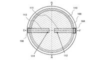
図1は照明装置の平面図であり、図2(A)は図1における線E−F、図2(B)は図1における線G−Hの断面図である。 1 is a plan view of the lighting device, FIG. 2A is a sectional view taken along line EF in FIG. 1, and FIG. 2B is a sectional view taken along line GH in FIG.
下地保護膜(バリア層)として絶縁膜102が設けられた基板100上に第1の電極層104、EL層106、及び第2の電極層108を含む発光素子132が形成され、発光素子132は第1の電極層104及び第2の電極層108の一部を除いて絶縁膜110に覆われている。絶縁膜110は発光素子のEL層106を外部からの水等の汚染物質から保護する保護膜、封止膜として機能する。なお、基板100は、丸型(ディスク形状、円盤型、または円形)形状を有しており、発光素子132を形成する為の薄膜が成膜できる部材を用いる。
A light-emitting
基板100は、丸型形状の基板であるため、基板100上に積層される絶縁膜102、第1の電極層104、EL層106、第2の電極層108、及び絶縁膜110もその形状を反映し、概略丸型形状に形成される。
Since the
第1の電極層104及び第2の電極層108は、絶縁膜110上に形成される第1の補助配線111、第2の補助配線113とそれぞれ接続するために、基板100の外周部まで延設しており、該延設領域において第1の電極層104、及び第2の電極層108は、絶縁膜110に覆われておらず露出している。この第1の電極層104及び第2の電極層108の露出領域は、それぞれ第1の電極層104と第1の補助配線111との接続部、第2の電極層108と第2の補助配線113との接続部となる。
The
第1の電極層104の延設された露出領域に接して第1の補助配線111が形成され、同様に第2の電極層108の延設された露出領域に接して第2の補助配線113が形成されている。第1の補助配線111及び第2の補助配線113は外部電源の端子との接続のための照明装置の端子として機能し、外部電源の端子との第1の接続部112(照明装置の第1の端子部ともいう)、第2の接続部114(照明装置の第2の端子部ともいう)を有している。第1の補助配線111及び第2の補助配線113によって、第1の電極層104の接続部である第1の接続部112、及び第2の電極層108の接続部である第2の接続部114は発光素子132と同一面上において円形の基板中央部に設けることができる。なお、本明細書において基板や照明装置の中央部とは中央及び中央付近を含む領域をいう。
The first
基板100の外周部Eにおいては、絶縁膜102上に、第1の電極層104が形成され、第1の電極層104上に第1の電極層104の端部を覆うようにEL層106が積層され、EL層106上にEL層106の端部を覆い基板100の外周部E側に延設して第2の電極層108が形成されている。第2の電極層108の延設された領域は、第2の電極層108上に積層される絶縁膜110は形成されず露出している。その露出した第2の電極層108に接して絶縁膜110上に第2の補助配線113が基板100中央部まで形成されている。よって第2の電極層108と電気的に接続した第2の補助配線113によって、基板100中央部に外部電源との第2の接続部114を形成することができる。
In the outer peripheral portion E of the
基板100の外周部Fにおいては、絶縁膜102上に、第1の電極層104が基板100の外周部F側に延設して形成されている。第1の電極層104上にEL層106、第2の電極層108が積層され、EL層106及び第2の電極層108上にEL層106及び第2の電極層108の端部を覆うように絶縁膜110が形成される。外周部Fにおいて、第1の電極層104の延設された領域は、第1の電極層104上に積層されるEL層106、第2の電極層108、及び絶縁膜110は形成されず露出している。その露出した第1の電極層104に接して絶縁膜110上に第1の補助配線111が基板100中央部まで形成されている。よって第1の電極層104と電気的に接続した第1の補助配線111によって、基板100中央部に外部電源との第1の接続部112を形成することができる。
In the outer peripheral portion F of the
基板100の外周部G及びHにおいては、絶縁膜102上に、第1の電極層104が形成され、第1の電極層104上に第1の電極層104を覆うようにEL層106が形成され、EL層106上に第2の電極層108が形成される。第1の電極層104、EL層106、及び第2の電極層108上に、EL層106及び第2の電極層108の端部を覆うように絶縁膜110が形成されている。
In the outer peripheral portions G and H of the
このように、照明装置において、EL層106は、第1の電極層104及び第2の電極層108が接しないように、第1の電極層104及び第2の電極層108の間に形成されている。また、EL層106の端部は、絶縁膜110又は第2の電極層108によって覆われる構造となっている。
As described above, in the lighting device, the
よって、発光素子132において、第1の電極層104及び第2の電極層108は接触によるショートを生じることなく、発光素子132から安定した発光を得ることができる。また、EL層が水等により劣化することを防ぎ、照明装置の信頼性を高めることができる。
Thus, in the light-emitting
本実施の形態の照明装置は、EL層106からの光を第1の電極層104、絶縁膜102、基板100を透過して取り出す照明装置である。よって、第1の電極層104、絶縁膜102、基板100は、EL層からの光を透過する透光性である必要である。なお、本明細書において透光性とは、少なくとも可視光の波長領域の光に対して光を透過する性質を指す。
The lighting device of this embodiment is a lighting device in which light from the
一方、第2の電極層108、絶縁膜110、第1の補助配線111、及び第2の補助配線113は必ずしも透光性を有する必要はない。第2の電極層108が反射性を有すると、EL層106から基板100側よりの光の取り出し効率を高めることができる。
On the other hand, the
基板100に用いる部材の具体例としては、プラスチック(可撓性基板)、ガラス、または、石英などを用いることができる。プラスチックとしては、例えば、ポリカーボネート、ポリアリレート、ポリエーテルスルフォン等からなる部材が挙げられる。また、フィルム(ポリプロピレン、ポリエステル、ビニル、ポリフッ化ビニル、ポリ塩化ビニルなどからなる)、無機蒸着フィルムを用いることもできる。なお、発光素子の作製工程における支持体として機能するものであれば、これら以外のものを用いることもできる。
As a specific example of a member used for the
また、基板100の大きさとしては、発光装置の用途によって適宜設定することが可能であるが、生産性、および取り扱いの面からCD−R等の光ディスクデバイスと同程度の大きさ(例えば、直径10cm乃至14cm、好ましくは直径12cmの円盤形状)とするのがより好ましい。
In addition, the size of the
よって、図1及び図2に示す照明装置は、直径10cm乃至14cm、好ましくは12cm、1.2mm乃至1.5mmの厚さの円盤形状を有する照明装置とすることができる。 Therefore, the lighting device illustrated in FIGS. 1 and 2 can be a lighting device having a disk shape with a diameter of 10 cm to 14 cm, preferably 12 cm and a thickness of 1.2 mm to 1.5 mm.
下地保護膜として機能する絶縁膜102は、例えば、無機化合物を用いて単層又は多層で形成する。無機化合物の代表例としては、酸化珪素、窒化珪素、酸化窒化珪素、窒化酸化珪素等がある。また、絶縁膜102として、硫化亜鉛及び酸化珪素を含む膜(ZnS・SiO2膜)を用いてもよい。なお、絶縁膜102として、窒化珪素、窒化酸化珪素、酸化窒化珪素等を用いることにより、外部からEL層へ、水分や酸素等の気体が侵入することを防止することができる。
The insulating
保護膜、封止膜として機能する絶縁膜110としては、例えば、無機化合物、有機化合物を用いて、単層又は多層で形成することができる。ここでは無機化合物を用いて単層又は多層で形成する。無機化合物の代表例としては、酸化珪素、窒化珪素、酸化窒化珪素、窒化酸化珪素、窒化アルミニウム、酸化窒化アルミニウム、窒化酸化アルミニウムまたは酸化アルミニウム、ダイアモンドライクカーボン(DLC)、窒素含有炭素等がある。また、絶縁膜110として、硫化亜鉛及び酸化珪素を含む膜(ZnS・SiO2膜)を用いてもよい。
As the insulating
また、有機化合物としては、ポリイミド、アクリル、ベンゾシクロブテン、ポリアミド、エポキシ等を用いることができる。また上記有機材料の他に、低誘電率材料(low−k材料)、シロキサン系樹脂、PSG(リンガラス)、BPSG(リンボロンガラス)等を用いることができる。 As the organic compound, polyimide, acrylic, benzocyclobutene, polyamide, epoxy, or the like can be used. In addition to the organic material, a low dielectric constant material (low-k material), a siloxane resin, PSG (phosphorus glass), BPSG (phosphorus boron glass), or the like can be used.
なおシロキサン系樹脂とは、シロキサン系材料を出発材料として形成されたSi−O−Si結合を含む樹脂に相当する。シロキサン系樹脂は置換基としては有機基(例えばアルキル基やアリール基)やフルオロ基を用いても良い。また、有機基はフルオロ基を有していても良い。 Note that the siloxane-based resin corresponds to a resin including a Si—O—Si bond formed using a siloxane-based material as a starting material. Siloxane resins may use organic groups (for example, alkyl groups and aryl groups) and fluoro groups as substituents. The organic group may have a fluoro group.
第1の補助配線111、第2の補助配線113は、導電性材料を用いればよく例えば、アルミニウム(Al)、チタン(Ti)、タンタル(Ta)、タングステン(W)、モリブデン(Mo)、クロム(Cr)、ネオジム(Nd)、スカンジウム(Sc)、ニッケル(Ni)、銅(Cu)から選ばれた材料又はこれらを主成分とする合金材料を用いて、単層で又は積層して形成することができる。また、酸化タングステンを含むインジウム酸化物、酸化タングステンを含むインジウム亜鉛酸化物、酸化チタンを含むインジウム酸化物、酸化チタンを含むインジウム錫酸化物、インジウム錫酸化物、インジウム亜鉛酸化物、酸化ケイ素を添加したインジウム錫酸化物などの導電性材料を用いてもよい。
The first
本実施の形態の照明装置は、簡便な製造工程による作製が可能であるので、量産化を実現することができる。また、本実施の形態の照明装置は、素子劣化しにくい構造を有するので長寿命な照明装置を提供することができる。さらに、本実施の形態の照明装置は、薄膜軽量化を実現すると共に外部電源との電気的な接続を容易にできるので、様々な用途に用いることができる。 Since the lighting device of this embodiment can be manufactured through a simple manufacturing process, mass production can be realized. In addition, since the lighting device of this embodiment has a structure in which element deterioration is unlikely to occur, a long-life lighting device can be provided. Furthermore, the lighting device of this embodiment can be used for various purposes because it can reduce the thickness of the thin film and can easily be electrically connected to an external power source.
(実施の形態2)
本実施の形態では、実施の形態1において、補助配線の構成が異なる照明装置の例を図3及び図4に示す。従って、他は実施の形態1と同様に行うことができ、実施の形態1と同一部分又は同様な機能を有する部分、及び工程の繰り返しの説明は省略する。
(Embodiment 2)
In this embodiment, an example of a lighting device having a different structure of the auxiliary wiring in
図3は照明装置の平面図であり、図4(A)は図3における線E−F、図4(B)は図3における線G−Hの断面図である。 3 is a plan view of the lighting device, FIG. 4A is a sectional view taken along line EF in FIG. 3, and FIG. 4B is a sectional view taken along line GH in FIG.
下地保護膜として絶縁膜102が設けられた基板100上に第1の電極層104、EL層106、及び第2の電極層108を含む発光素子132が形成され、発光素子132は第1の電極層104及び第2の電極層108の一部を除いて絶縁膜110に覆われている。
A light-emitting
第1の電極層104は、絶縁膜110上に形成される第1の補助配線111と接続するために、基板100の外周部まで延設しており、該延設領域において絶縁膜110には覆われておらず、第1の電極層104が露出している。第1の電極層104の延設された露出領域に接して第1の補助配線111が形成されている。第1の補助配線111は外部電源の端子との接続のための照明装置の端子として機能し、外部電源の端子との第1の接続部112を有している。
The
また、絶縁膜110は、第2の電極層108上に開口部を有しており、絶縁膜110の開口部において、第2の電極層108が露出している。この露出された第2の電極層108は外部電源の端子との接続のための照明装置の端子として機能し、外部電源の端子との第2の接続部114を有している。
The insulating
第1の補助配線111、及び絶縁膜110の開口部に露出された第2の電極層108によって、第1の電極層104の接続部である第1の接続部112、及び第2の電極層108の接続部である第2の接続部114は発光素子132と同一面上において円形の基板100中央部に設けることができる。
A
基板100の外周部Eにおいては、絶縁膜102上に、第1の電極層104が形成され、第1の電極層104上に第1の電極層104の端部を覆うようにEL層106が積層され、EL層106上にEL層106の端部を覆うように第2の電極層108が形成されている。第2の電極層108上には、第2の電極層108が外周部Eから中央部まで露出するように開口部を有する絶縁膜110が形成されている。よって第2の電極層108によって、基板100中央部に外部電源との第2の接続部114を形成することができる。
In the outer peripheral portion E of the
基板100の外周部Fにおいては、絶縁膜102上に、第1の電極層104が基板100の外周部F側に延設して形成されている。第1の電極層104上にEL層106、第2の電極層108が積層され、EL層106及び第2の電極層108上にEL層106及び第2の電極層108の端部を覆うように絶縁膜110が形成される。外周部Fにおいて、第1の電極層104の延設された領域は、第1の電極層104上に積層されるEL層106、第2の電極層108、絶縁膜110は形成されず露出している。その露出した第1の電極層104に接して絶縁膜110上に第1の補助配線111が基板100中央部まで形成されている。よって第1の電極層104と電気的に接続した第1の補助配線111によって、基板100中央部に外部電源との第1の接続部112を形成することができる。
In the outer peripheral portion F of the
基板100の外周部G及びHにおいては、絶縁膜102上に、第1の電極層104が形成され、第1の電極層104上に第1の電極層104を覆うようにEL層106が形成され、EL層106上に第2の電極層108が形成される。第1の電極層104、EL層106、及び第2の電極層108上に、EL層106、及び第2の電極層108の端部を覆うように絶縁膜110が形成されている。
In the outer peripheral portions G and H of the
このように、照明装置において、EL層106は、第1の電極層104及び第2の電極層108が接しないように、第1の電極層104及び第2の電極層108の間に形成されている。また、EL層106の端部は、絶縁膜110又は第2の電極層108によって覆われる構造となっている。
As described above, in the lighting device, the
よって、発光素子132において、第1の電極層104及び第2の電極層108は接触によるショートを生じることなく、発光素子132から安定した発光を得ることができる。また、EL層が水等により劣化することを防ぎ、照明装置の信頼性を高めることができる。
Thus, in the light-emitting
本実施の形態のように、発光素子の第1の電極層を第1の補助配線を用いて外部電源の第1の接続部を形成し、絶縁膜に開口を形成して第2の電極層に第2の接続部を形成してもよい。また、第1の接続部と第2の接続部を複数箇所設けてもよい。このように、照明装置において外部電源との接続部を設ける構成は、種々選択することができ、実施の形態1及び本実施の形態に限定されない。 As in this embodiment mode, the first electrode layer of the light-emitting element is formed using the first auxiliary wiring to form the first connection portion of the external power supply, and the opening is formed in the insulating film to form the second electrode layer. A second connection portion may be formed. Moreover, you may provide the 1st connection part and the 2nd connection part in multiple places. As described above, the structure in which the connection portion with the external power supply is provided in the lighting device can be variously selected and is not limited to the first embodiment and the present embodiment.
本実施の形態の照明装置は、簡便な製造工程による作製が可能であるので、量産化を実現することができる。また、本実施の形態の照明装置は、素子劣化しにくい構造を有するので長寿命な照明装置を提供することができる。さらに、本実施の形態の照明装置は、薄膜軽量化を実現すると共に外部電源との電気的な接続を容易にできるので、様々な用途に用いることができる。 Since the lighting device of this embodiment can be manufactured through a simple manufacturing process, mass production can be realized. In addition, since the lighting device of this embodiment has a structure in which element deterioration is unlikely to occur, a long-life lighting device can be provided. Furthermore, the lighting device of this embodiment can be used for various purposes because it can reduce the thickness of the thin film and can easily be electrically connected to an external power source.
(実施の形態3)
本実施の形態では、補助配線を用いない構成の照明装置の例を図5及び図6に示す。従って、他は実施の形態1と同様に行うことができ、実施の形態1及び実施の形態2と同一部分又は同様な機能を有する部分、及び工程の繰り返しの説明は省略する。
(Embodiment 3)
In this embodiment, an example of a lighting device having a structure in which no auxiliary wiring is used is illustrated in FIGS. Accordingly, the other steps can be performed in the same manner as in
図5は照明装置の平面図であり、図6(A)は図5における線X1−X2、図6(B)は図5における線Y1−Y2の断面図である。 5 is a plan view of the lighting device, FIG. 6A is a cross-sectional view taken along line X1-X2 in FIG. 5, and FIG. 6B is a cross-sectional view taken along line Y1-Y2 in FIG.
図5及び図6の照明装置には半円形状の発光素子が発光素子132a、発光素子132bと複数設けられており、中央部において、それぞれ第1の接続部112a、第2の接続部114a、第1の接続部112b、第2の接続部114bを有している。
5 and 6 includes a plurality of
基板100中央部には発光素子132a、132bは設けられず、第1の接続部112a、112b、第2の接続部114a、114bが設けられている。発光素子132aは、第1の電極層104a、EL層106a、及び第2の電極層108aの積層より構成され、発光素子132bは、第1の電極層104b、EL層106b、及び第2の電極層108bの積層より構成されている。
The
発光素子132aにおいて、第1の電極層104a及び第2の電極層108aは、基板100の中央部まで延設しており、該延設領域において絶縁膜110aは覆っておらず、第1の電極層104a、及び第2の電極層108aが露出して、第1の接続部112a、第2の接続部114aを形成している。同様に、発光素子132bにおいて、第1の電極層104b及び第2の電極層108bは、基板100の中央部まで延設しており、該延設領域において絶縁膜110bは覆っておらず、第1の電極層104b、及び第2の電極層108bが露出して、第1の接続部112b、第2の接続部114bを形成している。
In the light-emitting
図6(A)において、基板100の中央部の発光素子132a側では、絶縁膜102上に、第1の電極層104aが基板100の中央部に延設して形成されている。第1の電極層104a上にEL層106a、第2の電極層108aが積層され、EL層106a及び第2の電極層108a上にEL層106a及び第2の電極層108aの端部を覆うように絶縁膜110aが形成される。第1の電極層104aの延設された領域は、第1の電極層104a上に積層されるEL層106a、第2の電極層108a、絶縁膜110aは形成されず露出して、第1の接続部112aを形成している。同様に、基板100の中央部の発光素子132b側では、絶縁膜102上に、第1の電極層104bが基板100の中央部に延設して形成されている。第1の電極層104b上にEL層106b、第2の電極層108bが積層され、EL層106b及び第2の電極層108b上にEL層106b及び第2の電極層108bの端部を覆うように絶縁膜110bが形成される。第1の電極層104b上の延設された領域は、第1の電極層104bに積層されるEL層106b、第2の電極層108b、絶縁膜110bは形成されず露出して、第1の接続部112bを形成している。
6A, the
図6(B)において、基板100の中央部の発光素子132a側では、絶縁膜102上に、第1の電極層104aが形成され、第1の電極層104a上に第1の電極層104aの端部を覆うようにEL層106aが積層され、EL層106a上にEL層106aの端部を覆い基板100の中央部に延設して第2の電極層108aが形成されている。第2の電極層108aの延設された領域は、第2の電極層108a上に積層される絶縁膜110aは形成されず露出して、第2の接続部114aを形成している。同様に、基板100の中央部の発光素子132b側では、絶縁膜102上に、第1の電極層104bが形成され、第1の電極層104b上に第1の電極層104bの端部を覆うようにEL層106bが積層され、EL層106b上にEL層106bの端部を覆い基板100の中央部に延設して第2の電極層108bが形成されている。第2の電極層108bの延設された領域は、第2の電極層108b上に積層される絶縁膜110bは形成されず露出して、第2の接続部114bを形成している。
6B, the
基板100の外周部X1、及びY1においては、絶縁膜102上に、第1の電極層104aが形成され、第1の電極層104a上に第1の電極層104aを覆うようにEL層106aが形成され、EL層106a上に第2の電極層108aが形成される。第1の電極層104a、EL層106a、及び第2の電極層108a上に、EL層106a、及び第2の電極層108aの端部を覆うように絶縁膜110aが形成されている。同様に、基板100の外周部X2、及びY2においては、絶縁膜102上に、第1の電極層104bが形成され、第1の電極層104b上に第1の電極層104bを覆うようにEL層106bが形成され、EL層106b上に第2の電極層108bが形成される。第1の電極層104b、EL層106b、及び第2の電極層108b上に、EL層106b、及び第2の電極層108bの端部を覆うように絶縁膜110bが形成されている。
In the outer peripheral portions X1 and Y1 of the
このように、照明装置において、EL層106a、106bは、第1の電極層104a、104b及び第2の電極層108a、108bが接しないように、第1の電極層104a、104b及び第2の電極層108a、108bの間に形成されている。また、EL層106a、106bの端部は、絶縁膜110a、110b又は第2の電極層108a、108bによって覆われる構造となっている。
In this manner, in the lighting device, the EL layers 106a and 106b are formed so that the
よって、発光素子132a、132bにおいて、第1の電極層104a、104b及び第2の電極層108a、108bは接触によるショートを生じることなく、発光素子132a、132bから安定した発光を得ることができる。また、EL層106a、106bが水等により劣化することを防ぎ、照明装置の信頼性を高めることができる。
Therefore, in the light-emitting
本実施の形態の照明装置は、簡便な製造工程による作製が可能であるので、量産化を実現することができる。また、本実施の形態の照明装置は、素子劣化しにくい構造を有するので長寿命な照明装置を提供することができる。さらに、本実施の形態の照明装置は、薄膜軽量化を実現すると共に外部電源との電気的な接続を容易にできるので、様々な用途に用いることができる。 Since the lighting device of this embodiment can be manufactured through a simple manufacturing process, mass production can be realized. In addition, since the lighting device of this embodiment has a structure in which element deterioration is unlikely to occur, a long-life lighting device can be provided. Furthermore, the lighting device of this embodiment can be used for various purposes because it can reduce the thickness of the thin film and can easily be electrically connected to an external power source.
(実施の形態4)
本実施の形態では、実施の形態1乃至3で示す照明装置と外部電源とを接続するために、照明装置に接続部材を設ける例を図7及び図8に示す。
(Embodiment 4)
In this embodiment, an example in which a connection member is provided in the lighting device in order to connect the lighting device described in any of
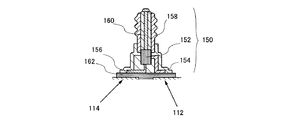
図8(A)(B)は照明装置に接続部材を設ける例であり、図7は照明装置と接続部材との接続部を詳細に説明する図である。 8A and 8B are examples in which a connection member is provided in the lighting device, and FIG. 7 is a diagram illustrating in detail a connection portion between the lighting device and the connection member.
図8(A)(B)において、照明装置130に接続部材150(口金ともいう)が取り付けられている。接続部材150は、制御回路152、第1の接続配線154、第2の接続配線156、第1の取り出し配線158、第2の取り出し配線160を有しており、照明装置130は、発光素子132を含み、絶縁膜110で接続部を除いて封止されている。照明装置130は、実施の形態1乃至3で示す照明装置を適用することができる。接続部材150は直径10mm〜40mm、代表的には25mm程度のものを用いればよい。実施の形態1乃至3に示す照明装置は、接続部材との接続部を中央部に設けているため、接続部材を照明装置中央部に設けることができる。
8A and 8B, a connection member 150 (also referred to as a base) is attached to the
図7に示すように、接続部材150は、照明装置130において発光素子132の第1の電極層と接続する第1の接続部112、第2の電極層と接続する第2の接続部114と、異方性導電膜162を介して電気的に接続する。第1の接続部112と第1の接続配線154、制御回路152を介して第1の取り出し配線158が電気的に接続し、第2の接続部114と第2の接続配線156、制御回路152を介して第2の取り出し配線160が電気的に接続する。接続部材150を外部電源に接続することで、外部電源より電力の供給を受けることができ、照明装置を点灯させることができる。
As shown in FIG. 7, the
制御回路152は、一例として、外部電源から供給される電源電圧を元に、発光素子132を一定の輝度で点灯させるための機能を有する回路である。制御回路152は、一例として、整流平滑回路、定電圧回路、定電流回路を有する。整流平滑回路は、外部の交流電源より供給される交流電圧を直流電圧にするための回路である。整流平滑回路は、一例として、ダイオードブリッジ回路、平滑容量等を組み合わせて構成すればよい。定電圧回路は、整流平滑回路から出力されるリップルを含んだ直流電圧を、安定化した定電圧の信号として出力する回路である。定電圧回路は、スイッチングレギュレータ、またはシリーズレギュレータ等を用いて構成すればよい。定電流回路は、定電圧回路の電圧に応じて定電流を発光素子132に出力する回路である。定電流回路は、トランジスタ等を用いて構成すればよい。なお、ここでは外部の電源として商用交流電源を想定し、整流平滑回路を設ける構成を示したが、外部の電源が直流電源の場合、整流平滑回路を設けなくてもよい。また、制御回路152には、必要に応じて、輝度を調整するための回路、サージ対策として保護回路等を設けてもよい。
As an example, the
図7では接続部材150と照明装置130の接続部との接続に異方性導電膜162を用いる例を示すが、接続部材150と照明装置130の接続部との電気的接続ができる方法及び構成ならばこれに限定されない。例えば、接続部材150及び照明装置130の接続部に用いる導電膜をはんだ接続が可能な材料で形成し、はんだを用いて接続してもよい。
Although FIG. 7 shows an example in which the anisotropic
図8(A)と図8(B)は、接続部材150の形状が異なるものであり、接続部材150は、照明装置130との電気的接続ができる接続配線及び外部電源より電力を供給できる取り出し配線を有していれば様々な形状を用いることができる。
8A and 8B are different in the shape of the
本実施の形態の照明装置は、簡便な製造工程による作製が可能であるので、量産化を実現することができる。また、本実施の形態の照明装置は、素子劣化しにくい構造を有するので長寿命な照明装置を提供することができる。さらに、本実施の形態の照明装置は、薄膜軽量化を実現すると共に外部電源との電気的な接続を容易にできるので、様々な用途に用いることができる。 Since the lighting device of this embodiment can be manufactured through a simple manufacturing process, mass production can be realized. In addition, since the lighting device of this embodiment has a structure in which element deterioration is unlikely to occur, a long-life lighting device can be provided. Furthermore, the lighting device of this embodiment can be used for various purposes because it can reduce the thickness of the thin film and can easily be electrically connected to an external power source.
本実施の形態は、他の実施の形態に記載した構成と適宜組み合わせて実施することが可能である。 This embodiment can be implemented in appropriate combination with the structures described in the other embodiments.
(実施の形態5)
本実施の形態では、実施の形態1乃至3で示す照明装置と外部電源とを接続するために照明装置に接続部材を設ける他の例を図9及び図10に示す。
(Embodiment 5)
In this embodiment mode, another example in which a connection member is provided in the lighting device in order to connect the lighting device described in any of
図9(A)(B)は、照明装置に接続部材を設ける例であり、図8(A)(B)において照明装置130の絶縁膜110上にさらに封止基板134を設け、発光素子132を封止する例である。
9A and 9B are examples in which a connection member is provided in the lighting device. In FIGS. 8A and 8B, a sealing
封止基板134によって発光素子132を基板100との間に封止することによって、外部からの水分や、発光素子を劣化させる物質が侵入することをさらに防止することができる。また、外部からの物理的な衝撃を緩和することができるため、照明装置として物理的強度を高めることができる。よって、照明装置の信頼性が向上するので、使用できる環境が広がり、多用途に用いることができる。
By sealing the light-emitting
図9(A)(B)の接続部材150が設けられた照明装置130の使用形態の例を図10(A)(B)に示す。図10(A)は接続部材150の形状に合わせて、天井140にねじ込み型で取り付ける例であり、図10(B)は天井140に引っ掛け型(引っ掛けシーリングともいう)で取り付ける例である。図10(A)(B)においても、接続部材150の第1の取り出し配線と第2の取り出し配線は、それぞれ第1の外部電極142、第2の外部電極144に電気的に接続し、電力を照明装置130に供給する。
FIGS. 10A and 10B show examples of usage patterns of the
封止基板134としては、発光素子132を挟持して対向する基板100と同様な形状が好ましく、丸型(ディスク形状、円盤型、または円形)形状を有するとよい。また、封止基板134は、接続部材150を取り付ける開口を有する。封止基板134を断面が凹型の形状にして、図9(A)(B)のように封止基板134内側に照明装置130をはめ込むようにすると好ましい。封止基板134の照明装置130側の面に乾燥剤となる吸水物質を設けてもよい。例えば、酸化バリウムなどの吸水物質の膜を封止基板134にスパッタ法により形成すればよい。このような乾燥剤として機能する膜は絶縁膜110上に形成してもよい。
The sealing
封止基板134に用いる部材の具体例としては、プラスチック(可撓性基板)、ガラス、石英、セラミックス、金属などを用いることができる。プラスチックとしては、例えば、ポリカーボネート、ポリアリレート、ポリエーテルスルフォン等からなる部材が挙げられる。また、フィルム(ポリプロピレン、ポリエステル、ビニル、ポリフッ化ビニル、ポリ塩化ビニルなどからなる)、無機蒸着フィルムを用いることもできる。なお、発光素子の封止基板として機能するものであれば、これら以外のものを用いることもできる。
As specific examples of the member used for the sealing
本実施の形態の照明装置は、簡便な製造工程による作製が可能であるので、量産化を実現することができる。また、本実施の形態の照明装置は、素子劣化しにくい構造を有するので長寿命な照明装置を提供することができる。さらに、本実施の形態の照明装置は、薄膜軽量化を実現すると共に外部電源との電気的な接続を容易にできるので、様々な用途に用いることができる。 Since the lighting device of this embodiment can be manufactured through a simple manufacturing process, mass production can be realized. In addition, since the lighting device of this embodiment has a structure in which element deterioration is unlikely to occur, a long-life lighting device can be provided. Furthermore, the lighting device of this embodiment can be used for various purposes because it can reduce the thickness of the thin film and can easily be electrically connected to an external power source.
(実施の形態6)
本実施の形態では、本発明の一態様である照明装置に用いる発光素子の素子構造の一例について、説明する。
(Embodiment 6)
In this embodiment, an example of an element structure of a light-emitting element used for the lighting device which is one embodiment of the present invention will be described.
図11(A)に示す素子構造は、一対の電極(陽極1001、陰極1002)間に発光領域を含むEL層1003が挟まれた構造を有する。
The element structure illustrated in FIG. 11A has a structure in which an
また、EL層1003は、少なくとも発光層1013を含んで形成されていればよく、発光層1013以外の機能層を含む積層構造であっても良い。発光層1013以外の機能層としては、正孔注入性の高い物質、正孔輸送性の高い物質、電子輸送性の高い物質、電子注入性の高い物質、バイポーラ性(電子及び正孔の輸送性の高い物質)の物質等を含む層を用いることができる。具体的には、正孔注入層1011、正孔輸送層1012、発光層1013、電子輸送層1014、電子注入層1015等の機能層を適宜組み合わせて用いることができる。
Further, the
次に、上述した発光素子に用いることができる材料について、具体的に説明する。 Next, materials that can be used for the light-emitting element described above will be specifically described.
陽極1001としては、仕事関数の大きい(具体的には4.0eV以上が好ましい。)金属、合金、電気伝導性化合物、およびこれらの混合物などを用いることが好ましい。具体的には、例えば、酸化インジウム−酸化スズ(ITO:Indium Tin Oxide)、珪素若しくは酸化珪素を含有した酸化インジウム−酸化スズ、酸化インジウム−酸化亜鉛(IZO:Indium Zinc Oxide)、酸化タングステン及び酸化亜鉛を含有した酸化インジウム等の導電性金属酸化物が挙げられる。
As the
これらの導電性金属酸化物膜は、通常スパッタにより成膜されるが、ゾル−ゲル法などを応用して作製しても構わない。例えば、酸化インジウム−酸化亜鉛(IZO)は、酸化インジウムに対し1〜20wt%の酸化亜鉛を加えたターゲットを用いてスパッタリング法により形成することができる。また、酸化タングステン及び酸化亜鉛を含有した酸化インジウムは、酸化インジウムに対し酸化タングステンを0.5〜5wt%、酸化亜鉛を0.1〜1wt%含有したターゲットを用いてスパッタリング法により形成することができる。 These conductive metal oxide films are usually formed by sputtering, but may be formed by applying a sol-gel method or the like. For example, indium oxide-zinc oxide (IZO) can be formed by a sputtering method using a target in which 1 to 20 wt% of zinc oxide is added to indium oxide. Further, indium oxide containing tungsten oxide and zinc oxide can be formed by a sputtering method using a target containing 0.5 to 5 wt% tungsten oxide and 0.1 to 1 wt% zinc oxide with respect to indium oxide. it can.
この他、陽極1001に用いられる材料としては、金(Au)、白金(Pt)、ニッケル(Ni)、タングステン(W)、クロム(Cr)、モリブデン(Mo)、鉄(Fe)、コバルト(Co)、銅(Cu)、パラジウム(Pd)、チタン(Ti)、または金属材料の窒化物(例えば、窒化チタン等)、モリブデン酸化物、バナジウム酸化物、ルテニウム酸化物、タングステン酸化物、マンガン酸化物、チタン酸化物等が挙げられる。
Other materials used for the
陰極1002としては、仕事関数の小さい(具体的には3.8eV以下であることが好ましい)金属、合金、電気伝導性化合物、およびこれらの混合物などを用いることができる。このような陰極材料の具体例としては、元素周期表の第1族または第2族に属する元素、すなわちリチウム(Li)やセシウム(Cs)等のアルカリ金属、およびマグネシウム(Mg)、カルシウム(Ca)、ストロンチウム(Sr)等のアルカリ土類金属、およびこれらを含む合金(MgAg、AlLi)、ユウロピウム(Eu)、イッテルビウム(Yb)等の希土類金属およびこれらを含む合金等が挙げられる。なお、アルカリ金属、アルカリ土類金属、これらを含む合金の膜は、真空蒸着法を用いて形成することができる。また、アルカリ金属またはアルカリ土類金属を含む合金はスパッタリング法により形成することも可能である。また、銀ペーストなどをインクジェット法などにより成膜することも可能である。
As the
この他、アルカリ金属化合物、アルカリ土類金属化合物、または希土類金属の化合物(例えば、フッ化リチウム(LiF)、酸化リチウム(LiOx)、フッ化セシウム(CsF)、フッ化カルシウム(CaF2)、フッ化エルビウム(ErF3)など)の薄膜と、アルミニウム等の金属膜とを積層することによって、陰極1002を形成することも可能である。
In addition, an alkali metal compound, an alkaline earth metal compound, or a rare earth metal compound (for example, lithium fluoride (LiF), lithium oxide (LiOx), cesium fluoride (CsF), calcium fluoride (CaF 2 ), fluorine The
なお、本実施の形態に示す発光素子において、陽極1001および陰極1002のうち、少なくとも一方が透光性を有すればよい。
Note that in the light-emitting element described in this embodiment, at least one of the
次に、EL層1003を構成する各層に用いる材料について、以下に具体例を示す。
Next, specific examples of materials used for each layer included in the
正孔注入層1011は、正孔注入性の高い物質を含む層である。正孔注入性の高い物質としては、例えば、モリブデン酸化物やバナジウム酸化物、ルテニウム酸化物、タングステン酸化物、マンガン酸化物等を用いることができる。この他、フタロシアニン(略称:H2Pc)や銅フタロシアニン(CuPc)等のフタロシアニン系の化合物、4,4’−ビス[N−(4−ジフェニルアミノフェニル)−N−フェニルアミノ]ビフェニル(略称:DPAB)、N,N’−ビス[4−[ビス(3−メチルフェニル)アミノ]フェニル]−N,N’−ジフェニル−[1,1’−ビフェニル]−4,4’−ジアミン(略称:DNTPD)等の芳香族アミン化合物、或いはポリ(3,4−エチレンジオキシチオフェン)/ポリ(スチレンスルホン酸)(PEDOT/PSS)等の高分子等によっても正孔注入層1011を形成することができる。さらに、トリス(p−エナミン置換−アミノフェニル)アミン化合物、2,7−ジアミノ−9−フルオレニリデン化合物、トリ(p−N−エナミン置換−アミノフェニル)ベンゼン化合物、アリール基が少なくとも1つ置換したエテニル基が一つ又は2つ置換したピレン化合物、N,N’−ジ(ビフェニル−4−イル)−N,N’−ジフェニルビフェニル−4,4’−ジアミン、N,N,N’,N’−テトラ(ビフェニル−4−イル)ビフェニル−4,4’−ジアミン、N,N,N’,N’−テトラ(ビフェニル−4−イル)−3,3’−ジエチルビフェニル−4,4’−ジアミン、2,2’−(メチレンジ−4,1−フェニレン)ビス[4,5−ビス(4−メトキシフェニル)−2H−1,2,3−トリアゾール]、2,2’−(ビフェニル−4,4’−ジイル)ビス(4,5−ジフェニル−2H−1,2,3−トリアゾール)、2,2’−(3,3’−ジメチルビフェニル−4,4’−ジイル)ビス(4,5−ジフェニル−2H−1,2,3−トリアゾール)、ビス[4−(4,5−ジフェニル−2H−1,2,3−トリアゾール−2−イル)フェニル](メチル)アミン等を用いて正孔注入層1011を形成することができる。
The
また、正孔注入層1011として、有機化合物と無機化合物(好ましくは、有機化合物に対して電子受容性を示す無機化合物)とを複合してなる正孔注入性複合材料を用いることができる。正孔注入性複合材料は、有機化合物と無機化合物との間で電子の授受が行われ、キャリア密度が増大するため、正孔注入性、正孔輸送性に優れている。
As the hole-
また、正孔注入層1011として正孔注入性複合材料を用いた場合、陽極1001とオーム接触をすることが可能となるため、仕事関数に関わらず陽極1001を形成する材料を選ぶことができる。
In addition, when a hole-injecting composite material is used for the hole-
正孔注入性複合材料に用いる無機化合物としては、遷移金属の酸化物であることが好ましい。また元素周期表における第4族乃至第8族に属する金属の酸化物を挙げることができる。具体的には、酸化バナジウム、酸化ニオブ、酸化タンタル、酸化クロム、酸化モリブデン、酸化タングステン、酸化マンガン、酸化レニウムは電子受容性が高いため好ましい。中でも特に、酸化モリブデンは大気中で安定であり、吸湿性が低く、扱いやすいため好ましい。 The inorganic compound used for the hole-injecting composite material is preferably a transition metal oxide. In addition, oxides of metals belonging to Groups 4 to 8 in the periodic table can be given. Specifically, vanadium oxide, niobium oxide, tantalum oxide, chromium oxide, molybdenum oxide, tungsten oxide, manganese oxide, and rhenium oxide are preferable because of their high electron accepting properties. Among these, molybdenum oxide is particularly preferable because it is stable in the air, has a low hygroscopic property, and is easy to handle.
正孔注入性複合材料に用いる有機化合物としては、芳香族アミン化合物、カルバゾール誘導体、芳香族炭化水素、高分子化合物(オリゴマー、デンドリマー、ポリマー等)など、種々の化合物を用いることができる。なお、正孔注入性複合材料に用いる有機化合物としては、正孔輸送性の高い有機化合物であることが好ましい。具体的には、10−6cm2/Vs以上の正孔移動度を有する物質であることが好ましい。但し、電子よりも正孔の輸送性の高い物質であれば、これら以外のものを用いてもよい。以下では、正孔注入性複合材料に用いることのできる有機化合物を具体的に列挙する。 As the organic compound used for the hole-injecting composite material, various compounds such as aromatic amine compounds, carbazole derivatives, aromatic hydrocarbons, and high molecular compounds (oligomers, dendrimers, polymers, and the like) can be used. Note that the organic compound used for the hole-injecting composite material is preferably an organic compound having a high hole-transport property. Specifically, a substance having a hole mobility of 10 −6 cm 2 / Vs or higher is preferable. Note that other than these substances, any substance that has a property of transporting more holes than electrons may be used. Hereinafter, organic compounds that can be used for the hole-injecting composite material are specifically listed.
例えば、芳香族アミン化合物としては、N,N’−ジ(p−トリル)−N,N’−ジフェニル−p−フェニレンジアミン(略称:DTDPPA)、4,4’−ビス[N−(4−ジフェニルアミノフェニル)−N−フェニルアミノ]ビフェニル(略称:DPAB)、N,N’−ビス[4−[ビス(3−メチルフェニル)アミノ]フェニル]−N,N’−ジフェニル−[1,1’−ビフェニル]−4,4’−ジアミン(略称:DNTPD)、1,3,5−トリス[N−(4−ジフェニルアミノフェニル)−N−フェニルアミノ]ベンゼン(略称:DPA3B)等を挙げることができる。 For example, as an aromatic amine compound, N, N′-di (p-tolyl) -N, N′-diphenyl-p-phenylenediamine (abbreviation: DTDPPA), 4,4′-bis [N- (4- Diphenylaminophenyl) -N-phenylamino] biphenyl (abbreviation: DPAB), N, N′-bis [4- [bis (3-methylphenyl) amino] phenyl] -N, N′-diphenyl- [1,1 '-Biphenyl] -4,4'-diamine (abbreviation: DNTPD), 1,3,5-tris [N- (4-diphenylaminophenyl) -N-phenylamino] benzene (abbreviation: DPA3B), etc. Can do.
正孔注入性複合材料に用いることのできるカルバゾール誘導体としては、具体的には、3−[N−(9−フェニルカルバゾール−3−イル)−N−フェニルアミノ]−9−フェニルカルバゾール(略称:PCzPCA1)、3,6−ビス[N−(9−フェニルカルバゾール−3−イル)−N−フェニルアミノ]−9−フェニルカルバゾール(略称:PCzPCA2)、3−[N−(1−ナフチル)−N−(9−フェニルカルバゾール−3−イル)アミノ]−9−フェニルカルバゾール(略称:PCzPCN1)等を挙げることができる。 As a carbazole derivative that can be used for the hole-injecting composite material, specifically, 3- [N- (9-phenylcarbazol-3-yl) -N-phenylamino] -9-phenylcarbazole (abbreviation: PCzPCA1), 3,6-bis [N- (9-phenylcarbazol-3-yl) -N-phenylamino] -9-phenylcarbazole (abbreviation: PCzPCA2), 3- [N- (1-naphthyl) -N -(9-phenylcarbazol-3-yl) amino] -9-phenylcarbazole (abbreviation: PCzPCN1) and the like can be given.
また、4,4’−ジ(N−カルバゾリル)ビフェニル(略称:CBP)、1,3,5−トリス[4−(N−カルバゾリル)フェニル]ベンゼン(略称:TCPB)、9−[4−(N−カルバゾリル)]フェニル−10−フェニルアントラセン(略称:CzPA)、1,4−ビス[4−(N−カルバゾリル)フェニル]−2,3,5,6−テトラフェニルベンゼン等を用いることができる。 In addition, 4,4′-di (N-carbazolyl) biphenyl (abbreviation: CBP), 1,3,5-tris [4- (N-carbazolyl) phenyl] benzene (abbreviation: TCPB), 9- [4- ( N-carbazolyl)] phenyl-10-phenylanthracene (abbreviation: CzPA), 1,4-bis [4- (N-carbazolyl) phenyl] -2,3,5,6-tetraphenylbenzene, and the like can be used. .
また、正孔注入性複合材料に用いることのできる芳香族炭化水素としては、例えば、2−tert−ブチル−9,10−ジ(2−ナフチル)アントラセン(略称:t−BuDNA)、2−tert−ブチル−9,10−ジ(1−ナフチル)アントラセン、9,10−ビス(3,5−ジフェニルフェニル)アントラセン(略称:DPPA)、2−tert−ブチル−9,10−ビス(4−フェニルフェニル)アントラセン(略称:t−BuDBA)、9,10−ジ(2−ナフチル)アントラセン(略称:DNA)、9,10−ジフェニルアントラセン(略称:DPAnth)、2−tert−ブチルアントラセン(略称:t−BuAnth)、9,10−ビス(4−メチル−1−ナフチル)アントラセン(略称:DMNA)、2−tert−ブチル−9,10−ビス[2−(1−ナフチル)フェニル]アントラセン、9,10−ビス[2−(1−ナフチル)フェニル]アントラセン、2,3,6,7−テトラメチル−9,10−ジ(1−ナフチル)アントラセン、2,3,6,7−テトラメチル−9,10−ジ(2−ナフチル)アントラセン、9,9’−ビアントリル、10,10’−ジフェニル−9,9’−ビアントリル、10,10’−ビス(2−フェニルフェニル)−9,9’−ビアントリル、10,10’−ビス[(2,3,4,5,6−ペンタフェニル)フェニル]−9,9’−ビアントリル、アントラセン、テトラセン、ルブレン、ペリレン、2,5,8,11−テトラ(tert−ブチル)ペリレン等が挙げられる。また、この他、ペンタセン、コロネン等も用いることができる。このように、1×10−6cm2/Vs以上の正孔移動度を有し、炭素数14〜42である芳香族炭化水素を用いることがより好ましい。 Examples of aromatic hydrocarbons that can be used for the hole-injecting composite material include 2-tert-butyl-9,10-di (2-naphthyl) anthracene (abbreviation: t-BuDNA), 2-tert -Butyl-9,10-di (1-naphthyl) anthracene, 9,10-bis (3,5-diphenylphenyl) anthracene (abbreviation: DPPA), 2-tert-butyl-9,10-bis (4-phenyl) Phenyl) anthracene (abbreviation: t-BuDBA), 9,10-di (2-naphthyl) anthracene (abbreviation: DNA), 9,10-diphenylanthracene (abbreviation: DPAnth), 2-tert-butylanthracene (abbreviation: t) -BuAnth), 9,10-bis (4-methyl-1-naphthyl) anthracene (abbreviation: DMNA), 2-tert-butyl Ru-9,10-bis [2- (1-naphthyl) phenyl] anthracene, 9,10-bis [2- (1-naphthyl) phenyl] anthracene, 2,3,6,7-tetramethyl-9,10 -Di (1-naphthyl) anthracene, 2,3,6,7-tetramethyl-9,10-di (2-naphthyl) anthracene, 9,9'-bianthryl, 10,10'-diphenyl-9,9 ' -Bianthryl, 10,10'-bis (2-phenylphenyl) -9,9'-bianthryl, 10,10'-bis [(2,3,4,5,6-pentaphenyl) phenyl] -9,9 Examples include '-bianthryl, anthracene, tetracene, rubrene, perylene, 2,5,8,11-tetra (tert-butyl) perylene, and the like. In addition, pentacene, coronene, and the like can also be used. Thus, it is more preferable to use an aromatic hydrocarbon having a hole mobility of 1 × 10 −6 cm 2 / Vs or more and having 14 to 42 carbon atoms.
なお、正孔注入性複合材料に用いることのできる芳香族炭化水素は、ビニル骨格を有していてもよい。ビニル基を有している芳香族炭化水素としては、例えば、4,4’−ビス(2,2−ジフェニルビニル)ビフェニル(略称:DPVBi)、9,10−ビス[4−(2,2−ジフェニルビニル)フェニル]アントラセン(略称:DPVPA)等が挙げられる。 Note that the aromatic hydrocarbon that can be used for the hole-injecting composite material may have a vinyl skeleton. As the aromatic hydrocarbon having a vinyl group, for example, 4,4′-bis (2,2-diphenylvinyl) biphenyl (abbreviation: DPVBi), 9,10-bis [4- (2,2- Diphenylvinyl) phenyl] anthracene (abbreviation: DPVPA) and the like.
また、ポリ(N−ビニルカルバゾール)(略称:PVK)やポリ(4−ビニルトリフェニルアミン)(略称:PVTPA)等の高分子化合物を用いることもできる。 Alternatively, a high molecular compound such as poly (N-vinylcarbazole) (abbreviation: PVK) or poly (4-vinyltriphenylamine) (abbreviation: PVTPA) can be used.
正孔輸送層1012は、正孔輸送性の高い物質を含む層である。正孔輸送性の高い物質としては、例えば、芳香族アミン(すなわち、ベンゼン環−窒素の結合を有するもの)の化合物であることが好ましい。広く用いられている材料として、4,4’−ビス[N−(3−メチルフェニル)−N−フェニルアミノ]ビフェニル、その誘導体である4,4’−ビス[N−(1−ナフチル)−N−フェニルアミノ]ビフェニル(以下、NPBと記す)、4,4’,4’’−トリス(N,N−ジフェニル−アミノ)トリフェニルアミン、4,4’,4’’−トリス[N−(3−メチルフェニル)−N−フェニルアミノ]トリフェニルアミンなどのスターバースト型芳香族アミン化合物が挙げられる。ここに述べた物質は、主に10−6cm2/Vs以上の正孔移動度を有する物質である。但し、電子よりも正孔の輸送性の高い物質であれば、これら以外のものを用いてもよい。なお、正孔輸送層1012は、単層のものだけでなく、上記物質の混合層、あるいは二層以上積層したものであってもよい。
The
また、PMMAのような電気的に不活性な高分子化合物に、正孔輸送性材料を添加してもよい。 Further, a hole transporting material may be added to an electrically inactive polymer compound such as PMMA.
また、ポリ(N−ビニルカルバゾール)(略称:PVK)やポリ(4−ビニルトリフェニルアミン)(略称:PVTPA)、ポリ[N−(4−{N’−[4−(4−ジフェニルアミノ)フェニル]フェニル−N’−フェニルアミノ}フェニル)メタクリルアミド](略称:PTPDMA)ポリ[N,N’−ビス(4−ブチルフェニル)−N,N’−ビス(フェニル)ベンジジン](略称:Poly−TPD)などの高分子化合物を用いてもよく、さらに上記高分子化合物に上記正孔輸送性材料を適宜添加してもよい。さらに、トリス(p−エナミン置換−アミノフェニル)アミン化合物、2,7−ジアミノ−9−フルオレニリデン化合物、トリ(p−N−エナミン置換−アミノフェニル)ベンゼン化合物、アリール基が少なくとも1つ置換したエテニル基が一つ又は2つ置換したピレン化合物、N,N’−ジ(ビフェニル−4−イル)−N,N’−ジフェニルビフェニル−4,4’−ジアミン、N,N,N’,N’−テトラ(ビフェニル−4−イル)ビフェニル−4,4’−ジアミン、N,N,N’,N’−テトラ(ビフェニル−4−イル)−3,3’−ジエチルビフェニル−4,4’−ジアミン、2,2’−(メチレンジ−4,1−フェニレン)ビス[4,5−ビス(4−メトキシフェニル)−2H−1,2,3−トリアゾール]、2,2’−(ビフェニル−4,4’−ジイル)ビス(4,5−ジフェニル−2H−1,2,3−トリアゾール)、2,2’−(3,3’−ジメチルビフェニル−4,4’−ジイル)ビス(4,5−ジフェニル−2H−1,2,3−トリアゾール)、ビス[4−(4,5−ジフェニル−2H−1,2,3−トリアゾール−2−イル)フェニル](メチル)アミン等も正孔輸送層1012に用いることができる。 In addition, poly (N-vinylcarbazole) (abbreviation: PVK), poly (4-vinyltriphenylamine) (abbreviation: PVTPA), poly [N- (4- {N ′-[4- (4-diphenylamino)] Phenyl] phenyl-N′-phenylamino} phenyl) methacrylamide] (abbreviation: PTPDMA) poly [N, N′-bis (4-butylphenyl) -N, N′-bis (phenyl) benzidine] (abbreviation: Poly -TPD) may be used, and the hole transport material may be appropriately added to the polymer compound. Further, tris (p-enamine substituted-aminophenyl) amine compound, 2,7-diamino-9-fluorenylidene compound, tri (pN-enamine substituted-aminophenyl) benzene compound, ethenyl substituted with at least one aryl group 1 or 2 substituted pyrene compounds, N, N′-di (biphenyl-4-yl) -N, N′-diphenylbiphenyl-4,4′-diamine, N, N, N ′, N ′ -Tetra (biphenyl-4-yl) biphenyl-4,4'-diamine, N, N, N ', N'-tetra (biphenyl-4-yl) -3,3'-diethylbiphenyl-4,4'- Diamine, 2,2 ′-(methylenedi-4,1-phenylene) bis [4,5-bis (4-methoxyphenyl) -2H-1,2,3-triazole], 2,2 ′-(biphenyl -4,4'-diyl) bis (4,5-diphenyl-2H-1,2,3-triazole), 2,2 '-(3,3'-dimethylbiphenyl-4,4'-diyl) bis ( 4,5-diphenyl-2H-1,2,3-triazole), bis [4- (4,5-diphenyl-2H-1,2,3-triazol-2-yl) phenyl] (methyl) amine and the like The hole-transport layer 1012 can be used.
発光層1013は、発光性の物質を含む層であり、種々の材料を用いることができる。例えば、発光性の物質としては、蛍光を発光する蛍光性化合物や燐光を発光する燐光性化合物を用いることができる。以下に、発光層に用いることのできる有機化合物材料を説明する。ただし、発光素子に適用可能な材料はこれらに限定されるものではない。
The
青色〜青緑色の発光は、例えば、ペリレン、2,5,8,11−テトラ−t−ブチルペリレン(略称:TBP)、9,10−ジフェニルアントラセンなどをゲスト材料として用い、適当なホスト材料に分散させることによって得られる。また、4,4’−ビス(2,2−ジフェニルビニル)ビフェニル(略称:DPVBi)などのスチリルアリーレン誘導体や、9,10−ジ−2−ナフチルアントラセン(略称:DNA)、9,10−ビス(2−ナフチル)−2−t−ブチルアントラセン(略称:t−BuDNA)などのアントラセン誘導体から得ることができる。また、ポリ(9,9−ジオクチルフルオレン)等のポリマーを用いても良い。また、青色発光のゲスト材料としては、スチリルアミン誘導体が好ましく、N,N’−ビス[4−(9H−カルバゾール−9−イル)フェニル]−N,N’−ジフェニルスチルベン−4,4’−ジアミン(略称:YGA2S)や、N,N’−ジフェニル−N,N’−ビス(9−フェニル−9H−カルバゾール−3−イル)スチルベン−4,4’−ジアミン(略称:PCA2S)などが挙げられる。特にYGA2Sは、450nm付近にピークを有しており好ましい。また、ホスト材料としては、アントラセン誘導体が好ましく、9,10−ビス(2−ナフチル)−2−t−ブチルアントラセン(略称:t−BuDNA)や、9−[4−(10−フェニル−9−アントリル)フェニル]−9H−カルバゾール(略称:CzPA)が好適である。特に、CzPAは電気化学的に安定であるため好ましい。 For example, perylene, 2,5,8,11-tetra-t-butylperylene (abbreviation: TBP), 9,10-diphenylanthracene is used as a guest material for blue to blue-green light emission as an appropriate host material. Obtained by dispersing. In addition, styrylarylene derivatives such as 4,4′-bis (2,2-diphenylvinyl) biphenyl (abbreviation: DPVBi), 9,10-di-2-naphthylanthracene (abbreviation: DNA), 9,10-bis It can be obtained from an anthracene derivative such as (2-naphthyl) -2-t-butylanthracene (abbreviation: t-BuDNA). A polymer such as poly (9,9-dioctylfluorene) may also be used. In addition, as the blue light emitting guest material, a styrylamine derivative is preferable, and N, N′-bis [4- (9H-carbazol-9-yl) phenyl] -N, N′-diphenylstilbene-4,4′- Examples include diamine (abbreviation: YGA2S) and N, N′-diphenyl-N, N′-bis (9-phenyl-9H-carbazol-3-yl) stilbene-4,4′-diamine (abbreviation: PCA2S). It is done. In particular, YGA2S is preferable because it has a peak in the vicinity of 450 nm. As the host material, an anthracene derivative is preferable, and 9,10-bis (2-naphthyl) -2-t-butylanthracene (abbreviation: t-BuDNA) or 9- [4- (10-phenyl-9-) is preferable. Anthryl) phenyl] -9H-carbazole (abbreviation: CzPA) is preferred. In particular, CzPA is preferable because it is electrochemically stable.
青緑色〜緑色の発光は、例えば、クマリン30、クマリン6などのクマリン系色素や、ビス[2−(2,4−ジフルオロフェニル)ピリジナト]ピコリナトイリジウム(略称:FIrpic)、ビス(2−フェニルピリジナト)アセチルアセトナトイリジウム(Ir(ppy)2(acac))などをゲスト材料として用い、適当なホスト材料に分散させることによって得られる。また、上述のペリレンやTBPを5wt%以上の高濃度で適当なホスト材料に分散させることによっても得られる。また、BAlq、Zn(BTZ)2、ビス(2−メチル−8−キノリノラト)クロロガリウム(Ga(mq)2Cl)などの金属錯体からも得ることができる。また、ポリ(p−フェニレンビニレン)等のポリマーを用いても良い。また、青緑色〜緑色の発光層のゲスト材料としては、アントラセン誘導体が効率の高い発光が得られるため好ましい。例えば、9,10−ビス{4−[N−(4−ジフェニルアミノ)フェニル−N−フェニル]アミノフェニル}−2−tert−ブチルアントラセン(略称:DPABPA)を用いることにより、高効率な青緑色発光が得られる。また、2位にアミノ基が置換されたアントラセン誘導体は高効率な緑色発光が得られるため好ましく、N−(9,10−ジフェニル−2−アントリル)−N,9−ジフェニル−9H−カルバゾール−3−アミン(略称:2PCAPA)が特に長寿命であり好適である。これらのホスト材料としてはアントラセン誘導体が好ましく、先に述べたCzPAが電気化学的に安定であるため好ましい。また、緑色発光と青色発光を組み合わせ、青色から緑色の波長領域に2つのピークを持つ発光素子を作製する場合、青色発光層のホストにCzPAのような電子輸送性のアントラセン誘導体を用い、緑色発光層のホストにNPBのようなホール輸送性の芳香族アミン化合物を用いると、青色発光層と緑色発光層との界面で発光が得られるため好ましい。すなわちこの場合、2PCAPAのような緑色発光材料のホストとしては、NPBの如き芳香族アミン化合物が好ましい。 Blue-green to green light emission is, for example, coumarin dyes such as coumarin 30 and coumarin 6, bis [2- (2,4-difluorophenyl) pyridinato] picolinatoiridium (abbreviation: FIrpic), bis (2-phenyl). Pyridinato) acetylacetonatoiridium (Ir (ppy) 2 (acac)) or the like is used as a guest material and dispersed in a suitable host material. It can also be obtained by dispersing the above-described perylene or TBP in a suitable host material at a high concentration of 5 wt% or more. It can also be obtained from metal complexes such as BAlq, Zn (BTZ) 2 , bis (2-methyl-8-quinolinolato) chlorogallium (Ga (mq) 2 Cl). A polymer such as poly (p-phenylene vinylene) may also be used. As a guest material for the blue-green to green light-emitting layer, an anthracene derivative is preferable because highly efficient light emission can be obtained. For example, by using 9,10-bis {4- [N- (4-diphenylamino) phenyl-N-phenyl] aminophenyl} -2-tert-butylanthracene (abbreviation: DPABPA), highly efficient blue-green Luminescence is obtained. An anthracene derivative having an amino group substituted at the 2-position is preferable because highly efficient green light emission can be obtained. N- (9,10-diphenyl-2-anthryl) -N, 9-diphenyl-9H-carbazole-3 An amine (abbreviation: 2PCAPA) is particularly preferable because of its long life. As these host materials, anthracene derivatives are preferable, and CzPA described above is preferable because it is electrochemically stable. When a light-emitting element having two peaks in the blue to green wavelength region is produced by combining green light emission and blue light emission, an electron-transporting anthracene derivative such as CzPA is used as the host of the blue light-emitting layer and green light emission is performed. When a hole transporting aromatic amine compound such as NPB is used for the host of the layer, light emission is preferably obtained at the interface between the blue light emitting layer and the green light emitting layer. That is, in this case, an aromatic amine compound such as NPB is preferable as the host of the green light emitting material such as 2PCAPA.
黄色〜橙色の発光は、例えば、ルブレン、4−(ジシアノメチレン)−2−[p−(ジメチルアミノ)スチリル]−6−メチル−4H−ピラン(略称:DCM1)、4−(ジシアノメチレン)−2−メチル−6−(9−ジュロリジル)エテニル−4H−ピラン(略称:DCM2)、ビス[2−(2−チエニル)ピリジナト]アセチルアセトナトイリジウム(Ir(thp)2(acac))、ビス(2−フェニルキノリナト)アセチルアセトナトイリジウム(Ir(pq)2(acac))などをゲスト材料として用い、適当なホスト材料に分散させることによって得られる。特に、ゲスト材料としてルブレンのようなテトラセン誘導体が、高効率かつ化学的に安定であるため好ましい。この場合のホスト材料としては、NPBのような芳香族アミン化合物が好ましい。他のホスト材料としては、ビス(8−キノリノラト)亜鉛(略称:Znq2)やビス[2−シンナモイル−8−キノリノラト]亜鉛(略称:Znsq2)などの金属錯体を用いることができる。また、ポリ(2,5−ジアルコキシ−1,4−フェニレンビニレン)等のポリマーを用いても良い。 Light emission of yellow to orange is, for example, rubrene, 4- (dicyanomethylene) -2- [p- (dimethylamino) styryl] -6-methyl-4H-pyran (abbreviation: DCM1), 4- (dicyanomethylene)- 2-methyl-6- (9-julolidyl) ethenyl-4H-pyran (abbreviation: DCM2), bis [2- (2-thienyl) pyridinato] acetylacetonatoiridium (Ir (thp) 2 (acac)), bis ( 2-phenylquinolinato) acetylacetonatoiridium (Ir (pq) 2 (acac)) or the like is used as a guest material and dispersed in a suitable host material. In particular, a tetracene derivative such as rubrene is preferable as a guest material because it is highly efficient and chemically stable. In this case, the host material is preferably an aromatic amine compound such as NPB. As another host material, a metal complex such as bis (8-quinolinolato) zinc (abbreviation: Znq 2 ) or bis [2-cinnamoyl-8-quinolinolato] zinc (abbreviation: Znsq 2 ) can be used. Further, a polymer such as poly (2,5-dialkoxy-1,4-phenylene vinylene) may be used.
橙色〜赤色の発光は、例えば、4−(ジシアノメチレン)−2,6−ビス[p−(ジメチルアミノ)スチリル]−4H−ピラン(略称:BisDCM)、4−(ジシアノメチレン)−2,6−ビス[2−(ジュロリジン−9−イル)エチニル]−4H−ピラン(略称:DCM1)、4−(ジシアノメチレン)−2−メチル−6−(9−ジュロリジル)エテニル−4H−ピラン(略称:DCM2)、ビス[2−(2−チエニル)ピリジナト]アセチルアセトナトイリジウム(略称:Ir(thp)2(acac))、などをゲスト材料として用い、適当なホスト材料に分散させることによって得られる。ビス(8−キノリノラト)亜鉛(略称:Znq2)やビス[2−シンナモイル−8−キノリノラト]亜鉛(略称:Znsq2)などの金属錯体からも得ることができる。また、ポリ(3−アルキルチオフェン)等のポリマーを用いても良い。赤色発光を示すゲスト材料としては、4−(ジシアノメチレン)−2,6−ビス[p−(ジメチルアミノ)スチリル]−4H−ピラン(略称:BisDCM)、4−(ジシアノメチレン)−2,6−ビス[2−(ジュロリジン−9−イル)エチニル]−4H−ピラン(略称:DCM1)、4−(ジシアノメチレン)−2−メチル−6−(9−ジュロリジル)エテニル−4H−ピラン(略称:DCM2)、{2−イソプロピル−6−[2−(2,3,6,7−テトラヒドロ−1,1,7,7−テトラメチル−1H,5H−ベンゾ[ij]キノリジン−9−イル)エテニル]−4H−ピラン−4−イリデン}プロパンジニトリル(略称:DCJTI)、{2,6−ビス[2−(2,3,6,7−テトラヒドロ−8−メトキシ−1,1,7,7−テトラメチル−1H,5H−ベンゾ[ij]キノリジン−9−イル)エテニル]−4H−ピラン−4−イリデン}プロパンジニトリル(略称:BisDCJTM)のような4H−ピラン誘導体が高効率であり、好ましい。特に、DCJTI、BisDCJTMは、620nm付近に発光ピークを有するため好ましい。 For example, 4- (dicyanomethylene) -2,6-bis [p- (dimethylamino) styryl] -4H-pyran (abbreviation: BisDCM), 4- (dicyanomethylene) -2,6 is emitted from orange to red. -Bis [2- (julolidin-9-yl) ethynyl] -4H-pyran (abbreviation: DCM1), 4- (dicyanomethylene) -2-methyl-6- (9-julolidyl) ethenyl-4H-pyran (abbreviation: DCM2), bis [2- (2-thienyl) pyridinato] acetylacetonatoiridium (abbreviation: Ir (thp) 2 (acac)), etc. are used as guest materials and dispersed in a suitable host material. It can also be obtained from a metal complex such as bis (8-quinolinolato) zinc (abbreviation: Znq 2 ) or bis [2-cinnamoyl-8-quinolinolato] zinc (abbreviation: Znsq 2 ). A polymer such as poly (3-alkylthiophene) may also be used. As guest materials that exhibit red light emission, 4- (dicyanomethylene) -2,6-bis [p- (dimethylamino) styryl] -4H-pyran (abbreviation: BisDCM), 4- (dicyanomethylene) -2,6 -Bis [2- (julolidin-9-yl) ethynyl] -4H-pyran (abbreviation: DCM1), 4- (dicyanomethylene) -2-methyl-6- (9-julolidyl) ethenyl-4H-pyran (abbreviation: DCM2), {2-isopropyl-6- [2- (2,3,6,7-tetrahydro-1,1,7,7-tetramethyl-1H, 5H-benzo [ij] quinolizin-9-yl) ethenyl ] -4H-pyran-4-ylidene} propanedinitrile (abbreviation: DCJTI), {2,6-bis [2- (2,3,6,7-tetrahydro-8-methoxy-1,1,7,7) -Te Ramechiru-1H, 5H-benzo [ij] quinolizine-9-yl) ethenyl] -4H- pyran-4-ylidene} propanedinitrile (abbreviation: BisDCJTM 4H-pyran derivative such as) is highly efficient and preferable. In particular, DCJTI and BisDCJTM are preferable because they have an emission peak near 620 nm.
なお、発光層1013としては、上述した発光性の物質(ゲスト材料)を他の物質(ホスト材料)に分散させた構成としてもよい。発光性の高い物質を分散させるための物質としては、各種のものを用いることができ、発光性の高い物質よりも最低空軌道準位(LUMO準位)が高く、最高被占有軌道準位(HOMO準位)が低い物質を用いることが好ましい。
Note that the light-emitting
発光性の物質を分散させるための物質としては、具体的には、トリス(8−キノリノラト)アルミニウム(III)(略称:Alq)、トリス(4−メチル−8−キノリノラト)アルミニウム(III)(略称:Almq3)、ビス(10−ヒドロキシベンゾ[h]キノリナト)ベリリウム(II)(略称:BeBq2)、ビス(2−メチル−8−キノリノラト)(4−フェニルフェノラト)アルミニウム(III)(略称:BAlq)、ビス(8−キノリノラト)亜鉛(II)(略称:Znq)、ビス[2−(2−ベンゾオキサゾリル)フェノラト]亜鉛(II)(略称:ZnPBO)、ビス[2−(2−ベンゾチアゾリル)フェノラト]亜鉛(II)(略称:ZnBTZ)などの金属錯体、2−(4−ビフェニリル)−5−(4−tert−ブチルフェニル)−1,3,4−オキサジアゾール(略称:PBD)、1,3−ビス[5−(p−tert−ブチルフェニル)−1,3,4−オキサジアゾール−2−イル]ベンゼン(略称:OXD−7)、3−(4−ビフェニリル)−4−フェニル−5−(4−tert−ブチルフェニル)−1,2,4−トリアゾール(略称:TAZ)、2,2’,2’’−(1,3,5−ベンゼントリイル)トリス(1−フェニル−1H−ベンゾイミダゾール)(略称:TPBI)、バソフェナントロリン(略称:BPhen)、バソキュプロイン(略称:BCP)などの複素環化合物や、9−[4−(10−フェニル−9−アントリル)フェニル]−9H−カルバゾール(略称:CzPA)、3,6−ジフェニル−9−[4−(10−フェニル−9−アントリル)フェニル]−9H−カルバゾール(略称:DPCzPA)、9,10−ビス(3,5−ジフェニルフェニル)アントラセン(略称:DPPA)、9,10−ジ(2−ナフチル)アントラセン(略称:DNA)、2−tert−ブチル−9,10−ジ(2−ナフチル)アントラセン(略称:t−BuDNA)、9,9’−ビアントリル(略称:BANT)、9,9’−(スチルベン−3,3’−ジイル)ジフェナントレン(略称:DPNS)、9,9’−(スチルベン−4,4’−ジイル)ジフェナントレン(略称:DPNS2)、3,3’,3’’−(ベンゼン−1,3,5−トリイル)トリピレン(略称:TPB3)、9,10−ジフェニルアントラセン(略称:DPAnth)、6,12−ジメトキシ−5,11−ジフェニルクリセンなどの縮合芳香族化合物、N,N−ジフェニル−9−[4−(10−フェニル−9−アントリル)フェニル]−9H−カルバゾール−3−アミン(略称:CzA1PA)、4−(10−フェニル−9−アントリル)トリフェニルアミン(略称:DPhPA)、N,9−ジフェニル−N−[4−(10−フェニル−9−アントリル)フェニル]−9H−カルバゾール−3−アミン(略称:PCAPA)、N,9−ジフェニル−N−{4−[4−(10−フェニル−9−アントリル)フェニル]フェニル}−9H−カルバゾール−3−アミン(略称:PCAPBA)、N−(9,10−ジフェニル−2−アントリル)−N,9−ジフェニル−9H−カルバゾール−3−アミン(略称:2PCAPA)、NPB(またはα−NPD)、TPD、DFLDPBi、BSPBなどの芳香族アミン化合物などを用いることができる。 As a substance for dispersing a light-emitting substance, specifically, tris (8-quinolinolato) aluminum (III) (abbreviation: Alq), tris (4-methyl-8-quinolinolato) aluminum (III) (abbreviation) : Almq 3), bis (10-hydroxybenzo [h] quinolinato) beryllium (II) (abbreviation: BeBq 2), and bis (2-methyl-8-quinolinolato) (4-phenylphenolato) aluminum (III) (abbreviation : BAlq), bis (8-quinolinolato) zinc (II) (abbreviation: Znq), bis [2- (2-benzoxazolyl) phenolato] zinc (II) (abbreviation: ZnPBO), bis [2- (2 -Benzothiazolyl) phenolato] zinc (II) (abbreviation: ZnBTZ) and other metal complexes, 2- (4-biphenylyl) -5- (4-te rt-butylphenyl) -1,3,4-oxadiazole (abbreviation: PBD), 1,3-bis [5- (p-tert-butylphenyl) -1,3,4-oxadiazole-2- Yl] benzene (abbreviation: OXD-7), 3- (4-biphenylyl) -4-phenyl-5- (4-tert-butylphenyl) -1,2,4-triazole (abbreviation: TAZ), 2,2 ', 2''-(1,3,5-benzenetriyl) tris (1-phenyl-1H-benzimidazole) (abbreviation: TPBI), bathophenanthroline (abbreviation: BPhen), bathocuproin (abbreviation: BCP), etc. Heterocyclic compounds, 9- [4- (10-phenyl-9-anthryl) phenyl] -9H-carbazole (abbreviation: CzPA), 3,6-diphenyl-9- [4- (10-phenyl-9) Anthryl) phenyl] -9H-carbazole (abbreviation: DPCzPA), 9,10-bis (3,5-diphenylphenyl) anthracene (abbreviation: DPPA), 9,10-di (2-naphthyl) anthracene (abbreviation: DNA) 2-tert-butyl-9,10-di (2-naphthyl) anthracene (abbreviation: t-BuDNA), 9,9′-bianthryl (abbreviation: BANT), 9,9 ′-(stilbene-3,3 ′ -Diyl) diphenanthrene (abbreviation: DPNS), 9,9 '-(stilbene-4,4'-diyl) diphenanthrene (abbreviation: DPNS2), 3,3', 3 ''-(benzene-1,3 5-triyl) tripyrene (abbreviation: TPB3), 9,10-diphenylanthracene (abbreviation: DPAnth), 6,12-dimethoxy-5,11-diphenylchrysene Condensed aromatic compounds such as N, N-diphenyl-9- [4- (10-phenyl-9-anthryl) phenyl] -9H-carbazol-3-amine (abbreviation: CzA1PA), 4- (10-phenyl- 9-anthryl) triphenylamine (abbreviation: DPhPA), N, 9-diphenyl-N- [4- (10-phenyl-9-anthryl) phenyl] -9H-carbazol-3-amine (abbreviation: PCAPA), N , 9-Diphenyl-N- {4- [4- (10-phenyl-9-anthryl) phenyl] phenyl} -9H-carbazol-3-amine (abbreviation: PCAPBA), N- (9,10-diphenyl-2 -Anthryl) -N, 9-diphenyl-9H-carbazol-3-amine (abbreviation: 2PCAPA), NPB (or α-NPD), TPD, DF DPbi, or the like can be used aromatic amine compounds such as BSPB.
また、発光性の物質を分散させるための物質は複数種用いることができる。例えば、結晶化を抑制するためにルブレン等の結晶化を抑制する物質をさらに添加してもよい。また、発光性の物質へのエネルギー移動をより効率良く行うためにNPB、あるいはAlq等をさらに添加してもよい。 In addition, a plurality of substances for dispersing the light-emitting substance can be used. For example, a substance that suppresses crystallization, such as rubrene, may be further added to suppress crystallization. Further, NPB, Alq, or the like may be further added in order to more efficiently transfer energy to the light emitting substance.
発光性の物質を他の物質に分散させた構成とすることにより、発光層1013の結晶化を抑制することができる。また、発光性の物質の濃度が高いことによる濃度消光を抑制することができる。
By using a structure in which a light-emitting substance is dispersed in another substance, crystallization of the light-emitting
電子輸送層1014は、電子輸送性の高い物質を含む層である。電子輸送性の高い物質としては、例えば、トリス(8−キノリノラト)アルミニウム(略称:Alq)、トリス(4−メチル−8−キノリノラト)アルミニウム(略称:Almq3)、ビス(10−ヒドロキシベンゾ[h]キノリナト)ベリリウム(略称:BeBq2)、ビス(2−メチル−8−キノリノラト)(4−フェニルフェノラト)アルミニウム(略称:BAlq)など、キノリン骨格またはベンゾキノリン骨格を有する金属錯体等からなる層である。また、この他ビス[2−(2−ヒドロキシフェニル)ベンゾオキサゾラト]亜鉛(略称:Zn(BOX)2)、ビス[2−(2−ヒドロキシフェニル)ベンゾチアゾラト]亜鉛(略称:Zn(BTZ)2)などのオキサゾール系、チアゾール系配位子を有する金属錯体なども用いることができる。さらに、金属錯体以外にも、2−(4−ビフェニリル)−5−(4−tert−ブチルフェニル)−1,3,4−オキサジアゾール(略称:PBD)や、1,3−ビス[5−(p−tert−ブチルフェニル)−1,3,4−オキサジアゾール−2−イル]ベンゼン(略称:OXD−7)、3−(4−ビフェニリル)−4−フェニル−5−(4−tert−ブチルフェニル)−1,2,4−トリアゾール(略称:TAZ)、バソフェナントロリン(略称:BPhen)、バソキュプロイン(略称:BCP)、ビス[3−(1H−ベンゾイミダゾール−2−イル)フルオレン−2−オラト]亜鉛(II)、ビス[3−(1H−ベンゾイミダゾール−2−イル)フルオレン−2−オラト]ベリリウム(II)、ビス[2−(1H−ベンゾイミダゾール−2−イル)ジベンゾ[b、d]フラン−3−オラト](フェノラト)アルミニウム(III)、ビス[2−(ベンゾオキサゾール−2−イル)−7,8−メチレンジオキシジベンゾ[b、d]フラン−3−オラト](2−ナフトラト)アルミニウム(III)なども用いることができる。ここに述べた物質は、主に10−6cm2/Vs以上の電子移動度を有する物質である。なお、正孔よりも電子の輸送性の高い物質であれば、上記以外の物質を電子輸送層1014として用いても構わない。また、電子輸送層1014は、単層のものだけでなく、上記物質からなる層が二層以上積層したものとしてもよい。
The
電子注入層1015は、電子注入性の高い物質を含む層である。電子注入性の高い物質としては、フッ化リチウム(LiF)、フッ化セシウム(CsF)、フッ化カルシウム(CaF2)等のアルカリ金属、アルカリ土類金属、またはこれらの化合物が挙げられる。また、有機化合物(好ましくは、電子輸送性を有する有機化合物)と無機化合物(好ましくは、アルカリ金属、アルカリ土類金属、希土類金属、またはそれらの化合物)とを複合してなる電子注入性複合材料を用いることもできる。電子注入性複合材料としては、例えばAlq中にマグネシウム(Mg)を含有させたもの等を用いることができる。この様な構造とすることにより、陰極1002からの電子注入効率をより高めることができる。
The
なお、電子注入層1015として、上述した電子注入性複合材料を用いた場合には、仕事関数に関わらずAl、Ag、ITO、珪素若しくは酸化珪素を含有したITO等様々な導電性材料を陰極1002の材料として用いることができる。
Note that in the case where the above-described electron injecting composite material is used as the
以上の層を適宜組み合わせて積層することにより、EL層1003を形成することができる。なお、発光層1013を2層以上の積層構造としても良い。発光層1013を2層以上の積層構造とし、各々の発光層に用いる発光物質の種類を変えることにより様々な発光色を得ることができる。また、発光物質として発光色の異なる複数の発光物質を用いることにより、ブロードなスペクトルの発光や白色発光を得ることもできる。特に、高輝度が必要とされる照明用途には、発光層を積層させた構造が好適である。
The
また、EL層1003の形成方法としては、用いる材料に応じて種々の方法(例えば、乾式法や湿式法等)適宜選択することができる。例えば、真空蒸着法、スパッタリング法、インクジェット法、スピンコート法、等を用いることができる。また、各層で異なる方法を用いて形成してもよい。
In addition, as a formation method of the
また、本実施の形態に示す発光素子の作製方法としては、ドライプロセス(例えば、真空蒸着法、スパッタリング法)、ウェットプロセス(例えば、インクジェット法、スピンコート法等)を問わず、種々の方法を用いて形成することができる。 In addition, as a method for manufacturing the light-emitting element described in this embodiment mode, various methods can be used regardless of a dry process (eg, a vacuum evaporation method or a sputtering method) or a wet process (eg, an inkjet method or a spin coating method). Can be formed.
なお、本実施の形態に示す発光素子の構成は、図11(B)に示すように一対の電極間にEL層1003が複数積層された構造、所謂、積層型素子の構成であってもよい。但し、EL層1003が、例えばn(nは2以上の自然数)層の積層構造を有する場合には、m(mは自然数、1≦m≦n−1)番目のEL層と、(m+1)番目のEL層との間には、それぞれ中間層1004が挟まれた構造を有する。
Note that the structure of the light-emitting element described in this embodiment may be a structure in which a plurality of
なお、中間層1004とは、陽極1001と陰極1002の間に電圧を印加したときに、中間層1004に接して形成される陽極1001側の一方のEL層1003に対して電子を注入する機能を有し、陰極1002側の他方のEL層1003に正孔を注入する機能を有する。
Note that the
中間層1004は、上述した有機化合物と無機化合物との複合材料(正孔注入性複合材料や電子注入性複合材料)の他、金属酸化物等の材料を適宜組み合わせて形成することができる。なお、正孔注入性複合材料とその他の材料とを組み合わせて用いることがより好ましい。中間層1004に用いるこれらの材料は、キャリア注入性、キャリア輸送性に優れているため、発光素子の低電流駆動、および低電圧駆動を実現することができる。
The
積層型素子の構成において、EL層が2層積層された構成を有する場合において、第1のEL層から得られる発光の発光色と第2のEL層から得られる発光の発光色を補色の関係にすることによって、白色発光を外部に取り出すことができる。なお、第1のEL層および第2のEL層のそれぞれが補色の関係にある複数の発光層を有する構成としても、白色発光が得られる。補色の関係としては、青色と黄色、あるいは青緑色と赤色などが挙げられる。青色、黄色、青緑色、赤色に発光する物質としては、例えば、先に列挙した発光物質の中から適宜選択すればよい。 In the structure of the stacked element, when the EL layer has a structure in which two layers are stacked, the emission color obtained from the first EL layer and the emission color obtained from the second EL layer are complementary to each other. By doing so, white light emission can be extracted to the outside. Note that white light emission can be obtained even when each of the first EL layer and the second EL layer includes a plurality of light-emitting layers having a complementary color relationship. Examples of complementary colors include blue and yellow or blue green and red. The substance that emits blue, yellow, blue-green, or red light may be appropriately selected from, for example, the light-emitting substances listed above.
以下に、第1のEL層および第2のEL層のそれぞれが補色の関係にある複数の発光層を有し、白色発光が得られる構成の一例を示す。 Hereinafter, an example of a structure in which each of the first EL layer and the second EL layer includes a plurality of light-emitting layers having a complementary color relationship and white light emission is obtained will be described.
例えば、第1のEL層は、青色〜青緑色の波長領域にピークを有する発光スペクトルを示す第1の発光層と、黄色〜橙色の波長領域にピークを有する発光スペクトルを示す第2の発光層とを有し、第2のEL層は、青緑色〜緑色の波長領域にピークを有する発光スペクトルを示す第3の発光層と、橙色〜赤色の波長領域にピークを有する発光スペクトルを示す第4の発光層とを有するものとする。 For example, the first EL layer includes a first light emitting layer having an emission spectrum having a peak in a blue to blue-green wavelength region, and a second light emitting layer having an emission spectrum having a peak in a yellow to orange wavelength region. The second EL layer has a third emission layer having an emission spectrum having a peak in the blue-green to green wavelength region, and a fourth emission spectrum having a peak in the orange to red wavelength region. And a light emitting layer.
この場合、第1のEL層からの発光は、第1の発光層および第2の発光層の両方からの発光を合わせたものであるので、青色〜青緑色の波長領域および黄色〜橙色の波長領域の両方にピークを有する発光スペクトルを示す。すなわち、第1のEL層は2波長型の白色または白色に近い色の発光を呈する。 In this case, since the light emission from the first EL layer is a combination of the light emission from both the first light emission layer and the second light emission layer, the wavelength region of blue to blue-green and the wavelength of yellow to orange are used. An emission spectrum having peaks in both regions is shown. That is, the first EL layer emits light of a two-wavelength type white color or a color close to white.
また、第2のEL層からの発光は、第3の発光層および第4の発光層の両方からの発光を合わせたものであるので、青緑色〜緑色の波長領域および橙色〜赤色の波長領域の両方にピークを有する発光スペクトルを示す。すなわち、第2のEL層は、第1のEL層とは異なる2波長型の白色または白色に近い色の発光を呈する。 In addition, since the light emission from the second EL layer is a combination of the light emission from both the third light emitting layer and the fourth light emitting layer, the blue-green to green wavelength region and the orange to red wavelength region are used. The emission spectrum which has a peak in both is shown. That is, the second EL layer emits light of a two-wavelength type white color or a color close to white which is different from that of the first EL layer.
したがって、第1のEL層からの発光および第2のEL層からの発光を重ね合わせることにより、青色〜青緑色の波長領域、青緑色〜緑色の波長領域、黄色〜橙色の波長領域、橙色〜赤色の波長領域をカバーする白色発光を得ることができる。 Therefore, by superimposing the light emission from the first EL layer and the light emission from the second EL layer, the blue to blue-green wavelength region, the blue-green to green wavelength region, the yellow to orange wavelength region, the orange to White light emission covering the red wavelength region can be obtained.
なお、上述した積層型素子の構成において、積層されるEL層の間に中間層を配置することにより、電流密度を低く保ったまま、高輝度領域での発光が可能である。電流密度を低く保てるため、長寿命素子を実現することができる。また、電極材料の抵抗による電圧降下を小さくできるので、大面積での均一発光が可能となる。 Note that in the above-described structure of the stacked element, an intermediate layer is disposed between stacked EL layers, whereby light emission in a high luminance region can be performed while keeping a current density low. Since the current density can be kept low, a long-life element can be realized. Further, since the voltage drop due to the resistance of the electrode material can be reduced, uniform light emission over a large area is possible.
なお、本実施の形態は、他の実施の形態と適宜組み合わせることが可能である。 Note that this embodiment can be combined with any of the other embodiments as appropriate.
(実施の形態7)
本実施の形態では、照明装置の応用例を示す。
(Embodiment 7)
In this embodiment, an application example of a lighting device is shown.
図12は、本発明の一態様である照明装置を室内の照明装置として用いた一例を示している。本発明の一態様である照明装置は、天井用照明装置8202としてのみならず、壁用照明装置8204としても用いることが可能である。また、当該照明装置は、卓上照明装置8206としても用いることが可能である。また本発明の一態様である照明装置は、面光源の光源を有するため、点光源の光源を用いた場合に比べ、光反射板等の部材を削減することができ、または熱の発生が白熱電球に比べて小さい点等、室内の照明装置として好ましい。
FIG. 12 illustrates an example in which the lighting device of one embodiment of the present invention is used as an indoor lighting device. The lighting device which is one embodiment of the present invention can be used not only as the
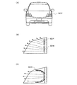
また、本発明の一態様である照明装置は、自動車、自転車などのヘッドライトとして用いることが可能である。図13(A)〜図13(C)は、本発明の一態様である照明装置を自動車のヘッドライトとして用いた一例を示している。図13(A)は、本発明の一態様である照明装置をヘッドライト8212として用いた自動車の外観図である。また図13(B)、図13(C)は、図13(A)のヘッドライト8212の断面図である。図13(B)、図13(C)において、電源供給用コネクタ8216に接続された照明装置8214は、光源として用いられている。図13(B)では、複数の照明装置8214が用いられているため高輝度の光を外部に取り出すことができる。一方、図13(C)では、反射板8218によって照明装置からの光が集光されており、指向性を有する高輝度の光を外部に取り出すことができる。
The lighting device which is one embodiment of the present invention can be used as a headlight for an automobile, a bicycle, or the like. 13A to 13C illustrate an example in which the lighting device which is one embodiment of the present invention is used as a headlight of an automobile. FIG. 13A is an external view of a car using the lighting device which is one embodiment of the present invention as the
次に、本発明の一態様である照明装置を、信号機、誘導灯等の照明装置として適用した例について図14(A)に示す。 Next, FIG. 14A illustrates an example in which the lighting device of one embodiment of the present invention is applied as a lighting device such as a traffic light or a guide light.
図14(A)は、一例として、信号機の外観について示した図である。信号機8228は、青の照明部8222、黄色の照明部8224、赤の照明部8226を有する。信号機8228は、各照明部における照明装置に青、黄、赤の三色に対応する本発明の一態様である照明装置を有する。
FIG. 14A is a diagram illustrating an appearance of a traffic light as an example. The
本発明の一態様である照明装置を避難口誘導灯に適用した例について図14(B)に示す。 FIG. 14B illustrates an example in which the lighting device of one embodiment of the present invention is applied to an escape exit guide light.
図14(B)は、一例として、避難口誘導灯の外観について示した図である。避難口誘導灯8232は、照明装置と、蛍光部が設けられた蛍光板とを組み合わせて構成することができる。また、特定の色を発光する照明装置と、図面のような形状の透過部が設けられた遮光板とを組み合わせて構成することもできる。本発明の一態様である照明装置は、一定の輝度で点灯することができるため、常時点灯が求められる避難口誘導灯として好ましい。 FIG. 14B is a diagram illustrating an appearance of an escape exit guide lamp as an example. The escape exit guide light 8232 can be configured by combining a lighting device and a fluorescent plate provided with a fluorescent part. Moreover, it can also comprise combining the illuminating device which light-emits a specific color, and the light-shielding plate provided with the transmission part of a shape like drawing. Since the lighting device which is one embodiment of the present invention can be lit at a constant luminance, it is preferable as an evacuation exit guide light that is always required to be lit.
本発明の一態様である照明装置を屋外用照明に適用した例について図14(C)に示す。 FIG. 14C illustrates an example in which the lighting device which is one embodiment of the present invention is applied to outdoor lighting.
屋外用照明の一つとして例えば街灯が挙げられる。街灯は、例えば図14(C)に示すように、筐体8242と、照明部8244と、を有する構成とすることができる。本発明の一態様である照明装置は、照明部8244に複数配置して用いることができる。図14(C)に示すように、街灯は、例えば道路沿いに設置して照明部8244により周囲を照らすことができるため、道路を含め周囲の視認性を向上させることができる。
One example of outdoor lighting is a streetlight. For example, as shown in FIG. 14C, the streetlight can include a
なお、街灯に電源電圧を供給する場合には、例えば図14(C)に示すように、電柱8246の送電線8248を介して電源電圧を供給することができる。ただしこれに限定されず、例えば光電変換装置を筐体8242に設け、光電変換装置により得られた電圧を電源電圧として利用することもできる。
In addition, when supplying a power supply voltage to a streetlight, a power supply voltage can be supplied through the
また、本発明の一態様である照明装置を携帯用照明に適用した例について図14(D)及び図14(E)に示す。図14(D)は、装着型ライトの構成を示す図であり、図14(E)は手持ち型ライトの構成を示す図である。 14D and 14E illustrate an example in which the lighting device which is one embodiment of the present invention is applied to portable lighting. FIG. 14D is a diagram illustrating a configuration of a wearable light, and FIG. 14E is a diagram illustrating a configuration of a handheld light.
Claims (9)
前記第1の電極と前記第2の電極の接続部を除いて前記発光素子を覆う保護層と、
前記保護層上に、前記第1の電極の接続部から前記基板の略中央部に配線される第1の補助配線及び前記第2の電極の接続部から前記基板の略中央部に配線される第2の補助配線と、
前記基板の略中央部に前記第1の補助配線から延設された第1の端子部及び前記第2の補助配線から延設された第2の端子部とを有する
ことを特徴とする照明装置。 The first electrode and the second electrode, and the first electrode and the second electrode, at least one of which has a light-transmitting property on one surface of the substrate having an insulating surface and has a connection portion at the outer peripheral portion of the substrate A light emitting element provided with an EL layer sandwiched between,
A protective layer covering the light-emitting element except for a connection portion between the first electrode and the second electrode;
On the protective layer, the first auxiliary wiring wired from the connection portion of the first electrode to the substantially central portion of the substrate and the wiring portion from the connection portion of the second electrode to the substantially central portion of the substrate. A second auxiliary wiring;
A lighting device comprising: a first terminal portion extending from the first auxiliary wiring; and a second terminal portion extending from the second auxiliary wiring at a substantially central portion of the substrate. .
前記発光素子を覆い前記基板の略中央部に開口部が設けられた保護層と、
前記保護層の開口部に設けられた、前記第1の電極から延設された第1の端子部及び前記第2の電極から延設された第2の端子部とを有する
ことを特徴とする照明装置。 On one surface of a substrate having an insulating surface, a first electrode and a second electrode, at least one of which has a light-transmitting property, and a layer containing a light-emitting material sandwiched between the first electrode and the second electrode A provided light emitting element;
A protective layer covering the light emitting element and having an opening provided in a substantially central portion of the substrate;
A first terminal portion extending from the first electrode and a second terminal portion extending from the second electrode are provided in the opening of the protective layer. Lighting device.
Priority Applications (1)
| Application Number | Priority Date | Filing Date | Title |
|---|---|---|---|
| JP2010056928A JP2010245030A (en) | 2009-03-18 | 2010-03-15 | Lighting device |
Applications Claiming Priority (2)
| Application Number | Priority Date | Filing Date | Title |
|---|---|---|---|
| JP2009066561 | 2009-03-18 | ||
| JP2010056928A JP2010245030A (en) | 2009-03-18 | 2010-03-15 | Lighting device |
Related Child Applications (1)
| Application Number | Title | Priority Date | Filing Date |
|---|---|---|---|
| JP2015030530A Division JP5996692B2 (en) | 2009-03-18 | 2015-02-19 | Lighting device |
Publications (2)
| Publication Number | Publication Date |
|---|---|
| JP2010245030A true JP2010245030A (en) | 2010-10-28 |
| JP2010245030A5 JP2010245030A5 (en) | 2013-04-18 |
Family
ID=42736925
Family Applications (2)
| Application Number | Title | Priority Date | Filing Date |
|---|---|---|---|
| JP2010056928A Withdrawn JP2010245030A (en) | 2009-03-18 | 2010-03-15 | Lighting device |
| JP2015030530A Active JP5996692B2 (en) | 2009-03-18 | 2015-02-19 | Lighting device |
Family Applications After (1)
| Application Number | Title | Priority Date | Filing Date |
|---|---|---|---|
| JP2015030530A Active JP5996692B2 (en) | 2009-03-18 | 2015-02-19 | Lighting device |
Country Status (2)
| Country | Link |
|---|---|
| US (2) | US8847480B2 (en) |
| JP (2) | JP2010245030A (en) |
Cited By (5)
| Publication number | Priority date | Publication date | Assignee | Title |
|---|---|---|---|---|
| JP2014089851A (en) * | 2012-10-29 | 2014-05-15 | Kaneka Corp | Power feeding structure of organic el panel |
| JP2014175229A (en) * | 2013-03-11 | 2014-09-22 | Kaneka Corp | Decorative member and decorative member for automotive interior and exterior trim |
| WO2015118591A1 (en) * | 2014-02-10 | 2015-08-13 | パナソニックIpマネジメント株式会社 | Planar luminescent body, planar luminescent module, and lighting device |
| WO2016136577A1 (en) * | 2015-02-26 | 2016-09-01 | コニカミノルタ株式会社 | Planar light-emitting module |
| JP2019040693A (en) * | 2017-08-23 | 2019-03-14 | スタンレー電気株式会社 | Vehicular lighting fixture |
Families Citing this family (12)
| Publication number | Priority date | Publication date | Assignee | Title |
|---|---|---|---|---|
| EP2230703A3 (en) | 2009-03-18 | 2012-05-02 | Semiconductor Energy Laboratory Co., Ltd. | Manufacturing apparatus and manufacturing method of lighting device |
| KR101849786B1 (en) | 2009-03-18 | 2018-04-17 | 가부시키가이샤 한도오따이 에네루기 켄큐쇼 | Lighting device |
| US8405116B2 (en) | 2009-03-18 | 2013-03-26 | Semiconductor Energy Laboratory Co., Ltd. | Lighting device |
| US8496341B2 (en) * | 2010-10-07 | 2013-07-30 | Semiconductor Energy Laboratory Co., Ltd. | Lighting device |
| JP5841406B2 (en) | 2010-11-05 | 2016-01-13 | 株式会社半導体エネルギー研究所 | Lighting device |
| KR20120119100A (en) * | 2011-04-20 | 2012-10-30 | 삼성디스플레이 주식회사 | Organic light emitting device |
| US10094549B2 (en) * | 2012-08-22 | 2018-10-09 | Flex-N-Gate Advanced Product Development, Llc | Micro-channel heat sink for LED headlamp |
| KR101551758B1 (en) * | 2012-12-11 | 2015-09-09 | 제일모직주식회사 | Composition for use of an anisotropic conductive film and an anisotropic conductive film thereof |
| DE102013107057B4 (en) | 2013-07-04 | 2022-05-25 | Pictiva Displays International Limited | Organic light-emitting diode and arrangement with such a light-emitting diode |
| JPWO2017056156A1 (en) * | 2015-09-28 | 2018-09-06 | パイオニア株式会社 | Light emitting system, light emitting device, and housing member |
| WO2018004618A1 (en) | 2016-06-30 | 2018-01-04 | Chavali Sri Chaitra Jyotsna | High density organic interconnect structures |
| US11239186B2 (en) | 2016-09-23 | 2022-02-01 | Intel Corporation | Die with embedded communication cavity |
Citations (9)
| Publication number | Priority date | Publication date | Assignee | Title |
|---|---|---|---|---|
| JPS595594A (en) * | 1982-06-30 | 1984-01-12 | 日本精機株式会社 | Field light emitting element |
| JPS62219492A (en) * | 1986-03-19 | 1987-09-26 | 日本電気株式会社 | El device |
| JPH0416897U (en) * | 1990-05-30 | 1992-02-12 | ||
| JPH0935873A (en) * | 1995-07-14 | 1997-02-07 | Matsushita Electric Ind Co Ltd | El lamp and manufacture thereof |
| JP2007005227A (en) * | 2005-06-27 | 2007-01-11 | Matsushita Electric Works Ltd | Surface light emitting panel, and lighting system |
| JP2007173424A (en) * | 2005-12-21 | 2007-07-05 | Matsushita Electric Works Ltd | Organic el lighting device |
| JP2007299674A (en) * | 2006-05-01 | 2007-11-15 | Matsushita Electric Works Ltd | Luminous panel lighting fixture |
| WO2008012460A2 (en) * | 2006-07-28 | 2008-01-31 | Saint-Gobain Glass France | Encapsulated electroluminescent device |
| JP2008034142A (en) * | 2006-07-26 | 2008-02-14 | Matsushita Electric Works Ltd | Organic electroluminescent light emitting device, and organic electroluminescent lighting system |
Family Cites Families (33)
| Publication number | Priority date | Publication date | Assignee | Title |
|---|---|---|---|---|
| JPH0416897A (en) | 1990-05-10 | 1992-01-21 | Mitsubishi Electric Corp | Multiwindow display system |
| US5757127A (en) * | 1994-06-10 | 1998-05-26 | Nippondenso Co., Ltd. | Transparent thin-film EL display apparatus with ambient light adaptation means |
| JPH0935571A (en) | 1995-07-14 | 1997-02-07 | Matsushita Electric Ind Co Ltd | Lighted switch unit |
| EP0996313A3 (en) | 1995-07-14 | 2000-08-02 | Matsushita Electric Industrial Co., Ltd. | Illuminated switch unit |
| TW387152B (en) | 1996-07-24 | 2000-04-11 | Tdk Corp | Solar battery and manufacturing method thereof |
| JP2002175877A (en) | 2000-09-27 | 2002-06-21 | Seiko Epson Corp | Organic electroluminescence device, manufacturing method of the organic electroluminescence device, and electronic equipment |
| US6664137B2 (en) * | 2001-03-29 | 2003-12-16 | Universal Display Corporation | Methods and structures for reducing lateral diffusion through cooperative barrier layers |
| JP2003203764A (en) * | 2001-10-25 | 2003-07-18 | Harison Toshiba Lighting Corp | Light emitting device |
| US6565231B1 (en) | 2002-05-28 | 2003-05-20 | Eastman Kodak Company | OLED area illumination lighting apparatus |
| US6787990B2 (en) | 2002-05-28 | 2004-09-07 | Eastman Kodak Company | OLED area illumination light source having flexible substrate on a support |
| US6771021B2 (en) | 2002-05-28 | 2004-08-03 | Eastman Kodak Company | Lighting apparatus with flexible OLED area illumination light source and fixture |
| JP2004047381A (en) * | 2002-07-15 | 2004-02-12 | Rohm Co Ltd | Flexible organic electroluminescent element, manufacturing method of same, information display device, and lighting device |
| US6936961B2 (en) * | 2003-05-13 | 2005-08-30 | Eastman Kodak Company | Cascaded organic electroluminescent device having connecting units with N-type and P-type organic layers |
| JP2005158372A (en) | 2003-11-25 | 2005-06-16 | Toyota Industries Corp | Electroluminescent element and illumination device |
| JP2005216495A (en) * | 2004-01-27 | 2005-08-11 | Matsushita Electric Works Ltd | Led unit with base |
| JP4027914B2 (en) | 2004-05-21 | 2007-12-26 | 株式会社半導体エネルギー研究所 | LIGHTING DEVICE AND DEVICE USING THE SAME |
| JP4820100B2 (en) * | 2005-03-01 | 2011-11-24 | 東北パイオニア株式会社 | Self-luminous panel, self-luminous panel manufacturing method, illumination and display device |
| JP2007018768A (en) | 2005-07-05 | 2007-01-25 | Toyota Industries Corp | Light emitting device, manufacturing method of the same, and liquid crystal display device |
| TWI291246B (en) | 2005-10-20 | 2007-12-11 | Epistar Corp | Light emitting device and method of forming the same |
| JP4792959B2 (en) | 2005-12-22 | 2011-10-12 | パナソニック電工株式会社 | Organic EL lighting panel and organic EL lighting device |
| JP4793075B2 (en) | 2006-04-21 | 2011-10-12 | パナソニック電工株式会社 | Lighting device |
| JP5112707B2 (en) | 2007-01-26 | 2013-01-09 | パナソニック株式会社 | Organic electroluminescence light emitting device |
| JP4293314B2 (en) | 2007-01-26 | 2009-07-08 | 財団法人山形県産業技術振興機構 | Lighting device |
| JP5135829B2 (en) * | 2007-03-02 | 2013-02-06 | 住友ベークライト株式会社 | Composite material substrate with transparent electrode |
| JP2008218309A (en) | 2007-03-07 | 2008-09-18 | Ngk Insulators Ltd | Manufacturing method of organic el substrate |
| JP2008218306A (en) | 2007-03-07 | 2008-09-18 | Pioneer Electronic Corp | Optical device |
| KR100890741B1 (en) * | 2007-03-13 | 2009-03-26 | 삼성전기주식회사 | High power light emitting diode package and fabrication method thereof |
| CN101926013B (en) | 2008-03-28 | 2012-09-26 | 松下电器产业株式会社 | Nitride semiconductor light-emitting device |
| EP2230703A3 (en) | 2009-03-18 | 2012-05-02 | Semiconductor Energy Laboratory Co., Ltd. | Manufacturing apparatus and manufacturing method of lighting device |
| KR101849786B1 (en) | 2009-03-18 | 2018-04-17 | 가부시키가이샤 한도오따이 에네루기 켄큐쇼 | Lighting device |
| US8405116B2 (en) | 2009-03-18 | 2013-03-26 | Semiconductor Energy Laboratory Co., Ltd. | Lighting device |
| EP2346094A1 (en) | 2010-01-13 | 2011-07-20 | FEI Company | Method of manufacturing a radiation detector |
| KR101182441B1 (en) | 2010-01-13 | 2012-09-12 | 삼성디스플레이 주식회사 | manufacturing method for organic thin film pattern and the manufacturing method for organic light emitting display apparatus |
-
2010
- 2010-03-12 US US12/722,791 patent/US8847480B2/en not_active Expired - Fee Related
- 2010-03-15 JP JP2010056928A patent/JP2010245030A/en not_active Withdrawn
-
2014
- 2014-09-19 US US14/491,025 patent/US9136492B2/en not_active Expired - Fee Related
-
2015
- 2015-02-19 JP JP2015030530A patent/JP5996692B2/en active Active
Patent Citations (10)
| Publication number | Priority date | Publication date | Assignee | Title |
|---|---|---|---|---|
| JPS595594A (en) * | 1982-06-30 | 1984-01-12 | 日本精機株式会社 | Field light emitting element |
| JPS62219492A (en) * | 1986-03-19 | 1987-09-26 | 日本電気株式会社 | El device |
| JPH0416897U (en) * | 1990-05-30 | 1992-02-12 | ||
| JPH0935873A (en) * | 1995-07-14 | 1997-02-07 | Matsushita Electric Ind Co Ltd | El lamp and manufacture thereof |
| JP2007005227A (en) * | 2005-06-27 | 2007-01-11 | Matsushita Electric Works Ltd | Surface light emitting panel, and lighting system |
| JP2007173424A (en) * | 2005-12-21 | 2007-07-05 | Matsushita Electric Works Ltd | Organic el lighting device |
| JP2007299674A (en) * | 2006-05-01 | 2007-11-15 | Matsushita Electric Works Ltd | Luminous panel lighting fixture |
| JP2008034142A (en) * | 2006-07-26 | 2008-02-14 | Matsushita Electric Works Ltd | Organic electroluminescent light emitting device, and organic electroluminescent lighting system |
| WO2008012460A2 (en) * | 2006-07-28 | 2008-01-31 | Saint-Gobain Glass France | Encapsulated electroluminescent device |
| JP2009545113A (en) * | 2006-07-28 | 2009-12-17 | サン−ゴバン グラス フランス | Encapsulated light emitting device |
Cited By (5)
| Publication number | Priority date | Publication date | Assignee | Title |
|---|---|---|---|---|
| JP2014089851A (en) * | 2012-10-29 | 2014-05-15 | Kaneka Corp | Power feeding structure of organic el panel |
| JP2014175229A (en) * | 2013-03-11 | 2014-09-22 | Kaneka Corp | Decorative member and decorative member for automotive interior and exterior trim |
| WO2015118591A1 (en) * | 2014-02-10 | 2015-08-13 | パナソニックIpマネジメント株式会社 | Planar luminescent body, planar luminescent module, and lighting device |
| WO2016136577A1 (en) * | 2015-02-26 | 2016-09-01 | コニカミノルタ株式会社 | Planar light-emitting module |
| JP2019040693A (en) * | 2017-08-23 | 2019-03-14 | スタンレー電気株式会社 | Vehicular lighting fixture |
Also Published As
| Publication number | Publication date |
|---|---|
| JP2015122333A (en) | 2015-07-02 |
| JP5996692B2 (en) | 2016-09-21 |
| US20150008421A1 (en) | 2015-01-08 |
| US8847480B2 (en) | 2014-09-30 |
| US9136492B2 (en) | 2015-09-15 |
| US20100237774A1 (en) | 2010-09-23 |
Similar Documents
| Publication | Publication Date | Title |
|---|---|---|
| JP5996692B2 (en) | Lighting device | |
| US9397311B2 (en) | Lighting device | |
| JP5984985B2 (en) | Lighting device | |
| KR101974082B1 (en) | Light-emitting device and lighting device | |
| JP5897859B2 (en) | Lighting device | |
| US9226359B2 (en) | Lighting device | |
| US9887175B2 (en) | Lighting device | |
| JP2010245036A (en) | Manufacturing device and manufacturing method of lighting device | |
| JP6261663B2 (en) | Light emitting device |
Legal Events
| Date | Code | Title | Description |
|---|---|---|---|
| A521 | Request for written amendment filed |
Free format text: JAPANESE INTERMEDIATE CODE: A523 Effective date: 20130306 |
|
| A621 | Written request for application examination |
Free format text: JAPANESE INTERMEDIATE CODE: A621 Effective date: 20130306 |
|
| A977 | Report on retrieval |
Free format text: JAPANESE INTERMEDIATE CODE: A971007 Effective date: 20131021 |
|
| A131 | Notification of reasons for refusal |
Free format text: JAPANESE INTERMEDIATE CODE: A131 Effective date: 20131029 |
|
| A521 | Request for written amendment filed |
Free format text: JAPANESE INTERMEDIATE CODE: A523 Effective date: 20131223 |
|
| A131 | Notification of reasons for refusal |
Free format text: JAPANESE INTERMEDIATE CODE: A131 Effective date: 20140722 |
|
| A521 | Request for written amendment filed |
Free format text: JAPANESE INTERMEDIATE CODE: A523 Effective date: 20140829 |
|
| A02 | Decision of refusal |
Free format text: JAPANESE INTERMEDIATE CODE: A02 Effective date: 20150127 |
|
| A761 | Written withdrawal of application |
Free format text: JAPANESE INTERMEDIATE CODE: A761 Effective date: 20150220 |