JP2010147542A - Data transmission circuit - Google Patents
Data transmission circuit Download PDFInfo
- Publication number
- JP2010147542A JP2010147542A JP2008319511A JP2008319511A JP2010147542A JP 2010147542 A JP2010147542 A JP 2010147542A JP 2008319511 A JP2008319511 A JP 2008319511A JP 2008319511 A JP2008319511 A JP 2008319511A JP 2010147542 A JP2010147542 A JP 2010147542A
- Authority
- JP
- Japan
- Prior art keywords
- unit
- video
- dummy
- signal
- input
- Prior art date
- Legal status (The legal status is an assumption and is not a legal conclusion. Google has not performed a legal analysis and makes no representation as to the accuracy of the status listed.)
- Withdrawn
Links
Images


Classifications
-
- H—ELECTRICITY
- H04—ELECTRIC COMMUNICATION TECHNIQUE
- H04N—PICTORIAL COMMUNICATION, e.g. TELEVISION
- H04N21/00—Selective content distribution, e.g. interactive television or video on demand [VOD]
- H04N21/40—Client devices specifically adapted for the reception of or interaction with content, e.g. set-top-box [STB]; Operations thereof
- H04N21/43—Processing of content or additional data, e.g. demultiplexing additional data from a digital video stream; Elementary client operations, e.g. monitoring of home network or synchronising decoder's clock; Client middleware
- H04N21/4302—Content synchronisation processes, e.g. decoder synchronisation
- H04N21/4305—Synchronising client clock from received content stream, e.g. locking decoder clock with encoder clock, extraction of the PCR packets
-
- H—ELECTRICITY
- H04—ELECTRIC COMMUNICATION TECHNIQUE
- H04N—PICTORIAL COMMUNICATION, e.g. TELEVISION
- H04N21/00—Selective content distribution, e.g. interactive television or video on demand [VOD]
- H04N21/20—Servers specifically adapted for the distribution of content, e.g. VOD servers; Operations thereof
- H04N21/23—Processing of content or additional data; Elementary server operations; Server middleware
- H04N21/234—Processing of video elementary streams, e.g. splicing of video streams or manipulating encoded video stream scene graphs
- H04N21/2347—Processing of video elementary streams, e.g. splicing of video streams or manipulating encoded video stream scene graphs involving video stream encryption
-
- H—ELECTRICITY
- H04—ELECTRIC COMMUNICATION TECHNIQUE
- H04N—PICTORIAL COMMUNICATION, e.g. TELEVISION
- H04N21/00—Selective content distribution, e.g. interactive television or video on demand [VOD]
- H04N21/20—Servers specifically adapted for the distribution of content, e.g. VOD servers; Operations thereof
- H04N21/23—Processing of content or additional data; Elementary server operations; Server middleware
- H04N21/236—Assembling of a multiplex stream, e.g. transport stream, by combining a video stream with other content or additional data, e.g. inserting a URL [Uniform Resource Locator] into a video stream, multiplexing software data into a video stream; Remultiplexing of multiplex streams; Insertion of stuffing bits into the multiplex stream, e.g. to obtain a constant bit-rate; Assembling of a packetised elementary stream
Landscapes
- Engineering & Computer Science (AREA)
- Multimedia (AREA)
- Signal Processing (AREA)
- Two-Way Televisions, Distribution Of Moving Picture Or The Like (AREA)
Abstract
【課題】従来のデータ送信回路においては、不正規な信号出力状態を検知できない、出画時間が遅れてしまうという課題があった。
【解決手段】映像音声信号処理部から入力されたVideoデータおよびピクセルクロックを解析し、正規の信号かどうかを判定した後、不正規の場合は内部で擬似的に生成したダミーVideoデータおよびダミーピクセルクロックをもとにTMDSを生成し出力することで不正規信号出力状態を阻止することができ、また機器認証が発生しないため出画を早めることができる。
【選択図】図2In a conventional data transmission circuit, there is a problem that an irregular signal output state cannot be detected and an image output time is delayed.
Dummy video data and dummy pixels that are pseudo-generated internally in the case of irregularity after analyzing video data and pixel clock input from a video / audio signal processing unit and determining whether or not the signal is legitimate. By generating and outputting TMDS based on the clock, it is possible to prevent an illegal signal output state, and since device authentication does not occur, output can be accelerated.
[Selection] Figure 2
Description
本発明は、外部入力信号に応じてダミーデータに出力を切り替えるデータ送信回路等に関するものである。 The present invention relates to a data transmission circuit that switches output to dummy data in accordance with an external input signal.
近年デジタル化が進み、デジタルコンテンツを扱う機器間では非圧縮で高速デジタル伝送が可能なインターフェースであるHDMI(High-Definition Multimedia Interface)による通信が行われている。HDMIはTMDS(Transition Minimized Differential Signaling)という技術を用いてデータの高速転送を行う。TMDSは4種類のチャネルを用いてデータ送信を行い、それぞれRGBの3種類の色信号とクロック周波数の同期信号が割り当てられている。これらの信号情報およびクロック周波数はEIA-861-B規格(非特許文献1参照)で定められたものが使用される。 In recent years, digitalization has progressed, and communication using HDMI (High-Definition Multimedia Interface), which is an interface capable of non-compression and high-speed digital transmission, is performed between devices handling digital content. HDMI performs high-speed data transfer using a technology called TMDS (Transition Minimized Differential Signaling). TMDS transmits data using four types of channels, and each of the three types of RGB color signals and a clock frequency synchronization signal is assigned. As these signal information and clock frequency, those defined in the EIA-861-B standard (see Non-Patent Document 1) are used.
また、HDMIには、送信するコンテンツ情報を保護するために、HDCP(High-bandwidth Digital Content Protection system)規格(非特許文献2参照)で定められた機器認証およびコンテンツ保護が使用されている。 Also, in HDMI, device authentication and content protection defined by HDCP (High-bandwidth Digital Content Protection system) standard (see Non-Patent Document 2) are used to protect content information to be transmitted.
図1は、従来のHDMI通信システムの構成を示すブロック図である。図1に示すHDMI通信システムは、DVDプレーヤ等の送信機器100と、デジタルTV受信機等の受信機器120とを備える。送信機器100と受信機器120とは、HDMIケーブル130を介し接続される。
FIG. 1 is a block diagram showing a configuration of a conventional HDMI communication system. The HDMI communication system shown in FIG. 1 includes a
外部から送信用コンテンツ情報を取得するための手段は多く存在するが、図1の送信機器100では例として、DVDやSDなどのメディアから取得する場合はメディアドライブ101、電波情報から取得する場合はチューナー102を使用する。取得したコンテンツ情報は映像音声信号処理部103に入力され、映像音声信号処理部103は、RGBの3種類の色信号を含むVideoデータ,音声情報を含むAudioデータ,クロック周波数であるピクセルクロックの信号情報をHDMI LSIへ出力する。HDMI LSIでは、入力された信号情報に対して著作権保護部105で暗号化処理を行い、出力制御部106でTMDS信号に変換してHDMIケーブル130上に出力する。HDMI LSI内部の処理は制御レジスタ104経由で行われ、制御レジスタ104は映像音声信号処理部103内のCPUを用いて制御される。
There are many means for acquiring content information for transmission from the outside. For example, in the
送信機器100と受信機器120との間で機器認証を行い、受信中の情報を復号化するために必要な情報を取得した受信機器120は復号化を行い、映像出力や音声出力を行う。受信した情報の復号化には、ピクセルクロックとピクセルクロックに同期したVideoデータをもとに生成された復号化情報が必要となり、Videoデータまたはピクセルクロックが不正規な場合、正常に復号化情報が生成されないため認証エラーが発生する。このため、映像音声信号処理部103はVideoデータとピクセルクロックとを同期させてHDMI LSIへ入力し認証エラーの発生を防ぐ。
The
しかしながら、映像音声信号処理部103から入力された信号情報が何らかの問題により不正規な信号の状態であっても、従来の送信機器100では入力された信号情報に対して暗号化を行い、受信機器120に送信していた。受信機器120は受信したデータの復号化を実行するが、不正規な信号を用いて暗号化された情報のため、正常に復号化できず、認証エラーが発生し、再認証処理が実行され出画までに時間がかかる。仮に復号化できても信号が不正なため正常な映像にならないなどの現象が発生する。更には、映像音声信号処理部103が不正規な信号を出力しているということを検出できないため、不具合が発生している状況を回復することができない等の課題が発生した。
However, even if the signal information input from the video / audio
このような課題に対し、入力信号の水平同期信号Hsyncの間隔および垂直同期信号Vsyncの間隔をカウントし、出力信号情報として正しいかどうかを確認し、不正と判断した場合は出力を中断するという技術が特許文献1に記載されている。
しかしながら特許文献1の技術では、不正な信号の送信を防ぐことは可能となるが、不正規な信号を出力しているということを出力側が検出できないため、不具合が発生したままの状態になる。仮に検出できたとしても、送信機器と受信機器との間ではTMDS信号の再送処理が実行されるため機器認証が発生し、出画時間が遅れてしまうという課題があった。
However, in the technique of
本第一の発明のデータ送信回路は、入力されたデータを暗号化し、外部のデータ受信装置との機器認証を行う著作権保護部と、前記著作権保護部により暗号化されたデータをTMDS(Transition Minimized Differential Signaling)信号に変換し前記データ受信装置へ出力する出力制御部と、前記著作権保護部へ入力されるべきデータの出力フォーマット毎の設定情報を格納する情報格納部と、前記情報格納部に格納された設定情報と外部の映像音声信号処理部から入力されたピクセルクロックおよびVideoデータとを比較する信号解析部と、前記情報格納部に格納された設定情報をもとに、出力設定と同等の擬似的な信号としてダミーピクセルクロックおよびダミーVideoデータを生成するダミー信号生成部と、前記映像音声信号処理部から入力されたピクセルクロックと前記ダミー信号生成部により生成されたダミーピクセルクロックとのいずれを前記著作権保護部に入力するか,および,前記映像音声信号処理部から入力されたVideoデータと前記ダミー信号生成部により生成されたダミーVideoデータとのいずれを前記著作権保護部に入力するかを、前記信号解析部による比較結果に応じて切り替える信号切替部と、を備えたことを特徴とするデータ送信回路である。かかる構成により、不正な信号を検知したことを外部に通知することができ、更に機器認証が発生しないため出画を早めることができる。 The data transmission circuit according to the first aspect of the invention includes a copyright protection unit that encrypts input data and performs device authentication with an external data receiving device, and the data encrypted by the copyright protection unit is TMDS ( Transition Minimized Differential Signaling) output control unit that outputs to the data receiving device, an information storage unit that stores setting information for each output format of data to be input to the copyright protection unit, and the information storage A signal analysis unit that compares the setting information stored in the unit with the pixel clock and video data input from the external video / audio signal processing unit, and the output setting based on the setting information stored in the information storage unit A dummy signal generator for generating a dummy pixel clock and dummy video data as a pseudo signal equivalent to the image signal, and a pixel clock input from the video / audio signal processor. And the dummy pixel clock generated by the dummy signal generation unit is input to the copyright protection unit, and the video data input from the video / audio signal processing unit and the dummy signal generation unit A data transmission circuit comprising: a signal switching unit that switches which of the dummy video data is input to the copyright protection unit according to a comparison result by the signal analysis unit. With this configuration, it is possible to notify the outside that an illegal signal has been detected, and further, since device authentication does not occur, the image output can be accelerated.
また、本第二の発明のデータ送信回路は、第一の発明に対して、前記出力制御部は、前記ダミー信号生成部により生成されたダミーピクセルクロックおよびダミーVideoデータにもとづいたTMDS信号の出力中に、前記信号切替部が前記映像音声信号処理部から入力されたピクセルクロックおよびVideoデータを前記著作権保護部に入力すると切り替えたとき、前記ダミー信号生成部および前記映像音声信号処理部から出力されたピクセルクロックおよびVideoデータを連続して出力することを特徴とするデータ送信回路である。かかる構成により、TMDSの送信を停止させることなく信号を切り替えることができる。 Further, the data transmission circuit of the second aspect of the invention is the output of the TMDS signal based on the dummy pixel clock and the dummy video data generated by the dummy signal generation unit. When the signal switching unit switches to input the pixel clock and video data input from the video / audio signal processing unit to the copyright protection unit, the dummy signal generation unit and the video / audio signal processing unit output The data transmission circuit is characterized in that the output pixel clock and video data are continuously output. With this configuration, it is possible to switch signals without stopping TMDS transmission.
また、本第三の発明のデータ送信回路は、第二の発明に対して、前記出力制御部は、前記ダミー信号生成部から出力されたダミーピクセルクロックおよびダミーVideoデータにもとづいたTMDS信号の出力中に、前記信号切替部が前記映像音声信号処理部から入力されたピクセルクロックおよびVideoデータを前記著作権保護部に入力すると切り替えたとき、前記著作権保護部による前記データ受信装置との機器認証なしに前記映像音声信号処理部から入力されたピクセルクロックおよびVideoデータを出力することを特徴とするデータ送信回路である。かかる構成により、信号を切り替えても機器認証が発生しないため出画までの時間を早めることができる。 The data transmission circuit according to the third aspect of the present invention is the output of the TMDS signal based on the dummy pixel clock and the dummy video data output from the dummy signal generation unit. When the signal switching unit switches to input the pixel clock and video data input from the video / audio signal processing unit to the copyright protection unit, device authentication with the data receiving device by the copyright protection unit A data transmission circuit that outputs the pixel clock and the video data input from the video / audio signal processing unit without being transmitted. With this configuration, device authentication does not occur even when the signal is switched, so that the time until image output can be shortened.
また、本第四の発明のデータ送信回路は、第一の発明に対して、前記情報格納部に格納されている前記設定情報は、前記映像音声信号処理部からの入力によって変更可能であることを特徴とするデータ送信回路である。かかる構成により、規格や仕様変更等でフォーマット情報が更新された場合でも柔軟に対応することができる。 In the data transmission circuit of the fourth aspect of the invention, the setting information stored in the information storage unit can be changed by input from the video / audio signal processing unit. A data transmission circuit characterized by the above. With such a configuration, even when the format information is updated due to a change in standards or specifications, it is possible to flexibly cope with it.
また、本第五の発明のデータ送信回路は、第一の発明に対して、前記情報格納部、前記信号解析部および前記ダミー信号生成部の出力を制御する制御レジスタをさらに有することを特徴とするデータ送信回路である。かかる構成により、前記情報格納部においては内部で格納している設定情報を、制御レジスタを用いて更新することができ、前記信号解析部においては制御レジスタを用いて解析結果を外部に通知することができ、また前記情報格納部から取得する設定情報を、制御レジスタを用いて外部から取得することができ、前記ダミー信号生成部においては前記情報格納部から取得する設定情報を、制御レジスタを用いて外部から取得することができる。 According to a fifth aspect of the present invention, the data transmission circuit further includes a control register for controlling the outputs of the information storage unit, the signal analysis unit, and the dummy signal generation unit. A data transmission circuit. With this configuration, the setting information stored therein can be updated using the control register in the information storage unit, and the analysis result is notified to the outside using the control register in the signal analysis unit. The setting information acquired from the information storage unit can be acquired from the outside using a control register, and the dummy signal generation unit uses the control register to acquire the setting information acquired from the information storage unit. Can be obtained from outside.
また、本第六の発明のデータ送信回路は、第一の発明に対して、前記ダミー信号生成部は、発振器を用いてピクセルクロックおよびダミーVideoデータを生成することを特徴とするデータ送信回路である。かかる構成により、不正規な信号を入力された場合でも正常なTMDS信号を出力することができる。 The data transmission circuit according to a sixth aspect of the present invention is the data transmission circuit according to the first aspect, wherein the dummy signal generation unit generates a pixel clock and dummy video data using an oscillator. is there. With this configuration, a normal TMDS signal can be output even when an irregular signal is input.
本発明によるデータ送信回路によれば、不正な信号を検知したことを外部に通知することができ、更に機器認証が発生しないため出画を早めることができる。 According to the data transmission circuit of the present invention, it is possible to notify the outside that an illegal signal has been detected, and furthermore, since device authentication does not occur, the image output can be accelerated.
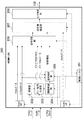
本発明の実施形態によるHDMI通信システムの概略構成は図1と同様である。ただし、本実施形態では、図1に示した送信機器100におけるHDMI LSIに代えて、図2に示すHDMI LSI200が適用される。図2に示すHDMI LSI200は、制御レジスタ201,発振器202,ダミー信号生成部203,情報格納部204,信号解析部205,信号切替部206,著作権保護部207および出力制御部208を具備する。
The schematic configuration of the HDMI communication system according to the embodiment of the present invention is the same as that shown in FIG. However, in the present embodiment, the
ダミー信号生成部203,情報格納部204,信号解析部205,信号切替部206,著作権保護部207,出力制御部208は、通常、ハードウェア(専用回路)で実現され得る。但し、MPUやメモリ等で実現し、処理手順は、通常、ソフトウェアで実現され、当該ソフトウェアはROM等の記録媒体に記録しても良い。
The dummy
著作権保護部207は、映像音声信号処理部103から入力されたデータを暗号化し、更に受信機器120との機器認証を行う。これらの処理は制御レジスタ201から発行される制御コマンドによって行う。ここで言うデータの暗号化および機器認証はHDCP規格に準拠する。著作権保護部207は機器認証結果を映像音声信号処理部103に通知してもよい。機器認証結果を通知する手段はさまざま存在するが、たとえば、制御レジスタ201内に認証結果を設定するレジスタが存在し、その値を映像音声信号処理部103が確認することで機器認証結果を知ることができる。もっとも通知手段はこれに限定されるものではなく、他の方法を用いてもよい。
The
出力制御部208は、著作権保護部207から入力されたデータをTMDS信号に変換し受信機器120へ出力する。出力する際、映像信号,音声信号に対してミュート処理を行うことが可能であり、これらの処理要求は、制御レジスタ201から発行される制御コマンドによって行う。ミュート状態になると、受信機器120の映像は黒が表示され、音声は無音状態になる。
The
情報格納部204は、著作権保護部207へ入力されるべきデータの出力フォーマット毎の設定情報を格納する。著作権保護部207へ入力されたVideo情報を確認する上で必要となる情報はさまざま存在するが、たとえば図3に示すように出力フォーマット情報をもとにEIA/CEA861-Bで定義されているV Active Lines,V Blanking Lines,H Active Pixels,H Blanking Pixels,Pixelクロック数を出力し、これらを用いることで信号情報を解析することができる。もっとも格納情報はこれに限定されるものではなく、他の方法を用いてもよい。また、格納情報の内容は外部から更新することができ、規格や仕様等の更新により出力フォーマット情報に変更が発生した場合でも順応に対応することができる。これらの処理は制御レジスタ201から発行される制御コマンドによって行う。
The
信号解析部205は、情報格納部204から入力された設定情報と映像音声信号処理部103から入力されたVideoデータおよびピクセルクロックとを比較し、当該比較結果を映像音声信号処理部103に通知する。比較手段はさまざま存在するが、たとえば、映像音声信号処理部103から入力されたVideoデータから水平同期信号数と垂直同期信号数を取得し、設定情報内の水平同期信号数(H Active Pixels,H Blanking Pixels),垂直同期信号数(V Active Lines,V Blanking Lines),Pixelクロック数と一致するかどうかを比較すればよい。もっとも比較手段はこれに限定されるものではなく、他の方法を用いてもよい。通知手段はさまざま存在するが、たとえば、制御レジスタ201内に比較結果を設定するレジスタが存在し、その値を映像音声信号処理部103が確認することで比較結果を知ることができる。もっとも通知手段はこれに限定されるものではなく、他の方法を用いてもよい。
The
また、信号解析部205は、信号切替部206に対して切替情報を通知する。切替情報には、Video I/Fから入力されているVideoデータ,ピクセルクロックを使用するか、ダミー信号生成部203から入力されているダミーVideoデータ,ダミーピクセルクロックを使用するかの情報が設定されている。これらの制御は、制御レジスタ201から発行される制御コマンドによって行う。
Further, the
ダミー信号生成部203は、情報格納部204から入力された設定情報をもとに、出力設定と同等の擬似的な信号としてダミーピクセルクロックとダミーVideoデータを生成する。ダミーピクセルクロックは発振器202を用いて生成し、生成する値は設定情報内のPixelクロック数と同値になる。ダミー信号生成部203は、発振器202から生成されたダミーピクセルクロックとダミーVideoデータとを同期させて出力する。これらの制御は、制御レジスタ201から発行される制御コマンドによって行う。
The dummy
信号切替部206は、Video I/Fから入力されているVideoデータ,ピクセルクロックを著作権保護部207に入力するか、ダミー信号生成部203から入力されているダミーVideoデータ,ダミーピクセルクロックを著作権保護部207に入力するかの切替処理を信号解析部205からの切替情報に基づいて行う。著作権保護部207にはピクセルクロックに同期したVideoデータを入力する必要があるため、同期処理は信号切替部206において行なわれる。なお、信号の同期をとる手段はさまざま存在する。たとえば、図4に示すように、信号切替部206内にVideoデータを一時的に蓄えるVideoメモリ400が存在し、切替情報が正規信号検出の場合、映像音声信号処理部103から入力されたVideoデータ401をVideoメモリ400に一旦蓄積し、映像音声信号処理部103から入力されたピクセルクロック402を用いて信号の同期処理を行い、Videoデータ401およびピクセルクロック402を出力信号用のVideoデータ405およびピクセルクロック406とする。また、切替情報が不正規信号検出の場合、ダミー信号生成部203が生成したダミーVideoデータ404とダミーピクセルクロック403を出力信号用のVideoデータ405およびピクセルクロック406とし、切替情報が正規信号検出になった時点でVideoメモリ400の情報を一旦クリアして、出力信号用のVideoデータ405をVideoデータ401に切り替え、ダミーピクセルクロック403を用いて信号の同期処理を行い、Videoデータ401およびダミーピクセルクロック403を出力信号用のVideoデータ405およびピクセルクロック406とすることができる。もっとも切替処理および同期処理はこれに限定されるものではなく、他の方法を用いてもよい。また、これらの制御は制御レジスタ201から発行される制御コマンドによって行う。
The
本実施形態によれば、HDMI LSI200は、以下のように、TMDS送信を中断させることなくVideo信号情報を切り替えることができる。
According to the present embodiment, the
HDMI LSI200は、映像音声信号処理部103から入力されたVideoデータとピクセルクロックを信号解析部205で解析し、正規か不正規かの結果を制御レジスタ201へ設定する。
The
信号解析部205による解析の結果、正規の信号が入力されている場合は、映像音声信号処理部103から入力されている信号を著作権保護部207へ入力し、出力制御部208がHDMI信号として出力処理を行う。
As a result of analysis by the
一方、信号解析部205による解析の結果、不正規の信号が入力されている場合、ダミー信号生成部203で生成されたダミーVideoデータとダミーピクセルクロックを著作権保護部207へ入力し、制御レジスタ201に映像信号のミュート設定を行う。これにより、出力制御部208は映像信号をミュートした状態でHDMI信号として出力する。ダミーVideoデータは受信機器120で映像として出力されるため、黒データにするのが望ましいが、他のデータでもよい。
On the other hand, if an illegal signal is input as a result of analysis by the
ダミーVideoデータを用いたHDMI信号を出力している間、映像音声信号処理部103は、信号解析部205からの解析結果を制御レジスタ201経由で取得し、解析結果が不正規信号検出の場合は再度信号を生成しVideoデータとピクセルクロックの再入力を行う。
While outputting the HDMI signal using the dummy video data, the video / audio
信号解析部205は入力信号を解析し、正規信号を検出した場合、切替情報を正規信号検出にする。これに応答して信号切替部206は、著作権保護部207に入力する信号をダミーVideoデータから映像音声信号処理部103から入力されているVideoデータへ切り替える。切り替え処理が完了すると信号切替部206は、制御レジスタ201に対して映像信号のミュート解除を設定する。
When the
出力制御部208は、制御レジスタ201に設定されたミュート解除により、出力中の映像信号に対してミュート解除処理を行う。
The
以上のように本実施形態によれば、HDMI LSI200は、TMDSの送信を中断させることなくVideo信号情報を切り替えることができる。
As described above, according to the present embodiment, the
本実施形態において、HDMI LSI200は、ダミーVideoデータを用いたHDMI信号を出力中に受信機器120との間で機器認証を行い、著作権保護部207で暗号化を施したデータを出力制御部208から出力することが可能である。受信機器120が受信中のダミーVideoデータを復号化中にHDMI LSI200が正規のVideoデータを再入力することでVideoデータの切替処理が発生するが、信号切替部206により出力するVideoデータとピクセルクロックとの同期がとれているため、切替処理後でも著作権保護部207では正常に暗号化処理を行うことができ、受信機器120では復号化処理中にエラーが発生しなくなる。これによりエラー発生による機器認証が発生しないため高速に受信機器120は映像を出力することができる。
In the present embodiment, the
本実施形態において、情報格納部204が内部で保持している設定情報を制御レジスタ201経由で内容を更新することができるようにしてもよい。これにより最新の設定情報を保持することが可能となる。また、設定情報を制御レジスタ201から取得し、取得内容を信号解析部205およびダミー信号生成部203で使用してもよい。
In the present embodiment, the contents of the setting information held in the
本実施形態において、各処理(各機能)は、単一の装置(システムや集積回路等)によって集中処理されることによって実現されてもよく、あるいは、複数の装置によって分散処理されることによって実現されてもよい。 In this embodiment, each process (each function) may be realized by centralized processing by a single device (system, integrated circuit, etc.), or by distributed processing by a plurality of devices. May be.
本発明は、以上の実施の形態に限定されることなく、種々の変更が可能であり、それらも本発明の範囲内に包含されるものであることは言うまでもない。 The present invention is not limited to the above-described embodiment, and various modifications are possible, and it goes without saying that these are also included in the scope of the present invention.
以上のように、本発明にかかるデータ送信回路は、不正な信号を検知したことを外部に通知することができ、更に機器認証が発生しないため出画を早めることができるという効果を有し、データ送信装置等として有用である。 As described above, the data transmission circuit according to the present invention can notify the outside that an illegal signal has been detected, and further has the effect of being able to speed up the image output because device authentication does not occur. It is useful as a data transmission device.
100…送信機器
101…メディアドライブ
102…チューナー
103…映像音声信号処理部
104,201…制御レジスタ
105,207…著作権保護部
106,208…出力制御部
120…受信機器
130…HDMIケーブル
200…データ送信回路
202…発振器
203…ダミー信号生成部
204…情報格納部
205…信号解析部
206…信号切替部
400…Videoメモリ
401…映像音声信号処理部103から入力されるVideoデータ
402…映像音声信号処理部103から入力されるピクセルクロック
403…ダミー信号生成部203から入力されるダミーピクセルクロック
404…ダミー信号生成部203から入力されるダミーVideoデータ
405…切替処理後のVideoデータ
406…切替処理後のピクセルクロック
100 ... Transmitting equipment
101 ... Media drive
102 ... Tuner
103 ... Video / audio signal processor
104,201 ... Control register
105,207… Copyright Protection Department
106,208 ... Output control unit
120 ... Receiving equipment
130 ... HDMI cable
200: Data transmission circuit
202 ... Oscillator
203 ... Dummy signal generator
204: Information storage
205 ... Signal analysis unit
206 ... Signal switching section
400… Video memory
401 ... Video data input from the video / audio
402 ... Pixel clock input from the video / audio
403 ... Dummy pixel clock input from the
404: Dummy video data input from the
405… Video data after switching
406 ... Pixel clock after switching
Claims (7)
前記著作権保護部により暗号化されたデータをTMDS(Transition Minimized Differential Signaling)信号に変換し前記データ受信装置へ出力する出力制御部と、
前記著作権保護部へ入力されるべきデータの出力フォーマット毎の設定情報を格納する情報格納部と、
前記情報格納部に格納された設定情報と外部の映像音声信号処理部から入力されたピクセルクロックおよびVideoデータとを比較する信号解析部と、
前記情報格納部に格納された設定情報をもとに、出力設定と同等の擬似的な信号としてダミーピクセルクロックおよびダミーVideoデータを生成するダミー信号生成部と、
前記映像音声信号処理部から入力されたピクセルクロックと前記ダミー信号生成部により生成されたダミーピクセルクロックとのいずれを前記著作権保護部に入力するか,および,前記映像音声信号処理部から入力されたVideoデータと前記ダミー信号生成部により生成されたダミーVideoデータとのいずれを前記著作権保護部に入力するかを、前記信号解析部による比較結果に応じて切り替える信号切替部と、
を備える、
ことを特徴とするデータ送信回路。 A copyright protection unit that encrypts input data and performs device authentication with an external data receiving device;
An output control unit that converts the data encrypted by the copyright protection unit into a TMDS (Transition Minimized Differential Signaling) signal and outputs the signal to the data receiving device;
An information storage unit for storing setting information for each output format of data to be input to the copyright protection unit;
A signal analysis unit that compares setting information stored in the information storage unit with a pixel clock and video data input from an external video / audio signal processing unit;
Based on the setting information stored in the information storage unit, a dummy signal generation unit that generates a dummy pixel clock and dummy video data as a pseudo signal equivalent to the output setting,
Which of the pixel clock input from the video / audio signal processing unit and the dummy pixel clock generated by the dummy signal generation unit is input to the copyright protection unit, and input from the video / audio signal processing unit Which of the video data and the dummy video data generated by the dummy signal generation unit is input to the copyright protection unit, a signal switching unit that switches according to the comparison result by the signal analysis unit,
Comprising
A data transmission circuit.
前記出力制御部は、
前記ダミー信号生成部により生成されたダミーピクセルクロックおよびダミーVideoデータにもとづいたTMDS信号の出力中に、前記信号切替部が前記映像音声信号処理部から入力されたピクセルクロックおよびVideoデータを前記著作権保護部に入力すると切り替えたとき、前記ダミー信号生成部および前記映像音声信号処理部から出力されたピクセルクロックおよびVideoデータを連続して出力する、
ことを特徴とするデータ送信回路。 In claim 1,
The output control unit
During output of the TMDS signal based on the dummy pixel clock and dummy video data generated by the dummy signal generation unit, the signal switching unit converts the pixel clock and video data input from the video / audio signal processing unit to the copyright. When switching to input to the protection unit, continuously output the pixel clock and video data output from the dummy signal generation unit and the video and audio signal processing unit,
A data transmission circuit.
前記出力制御部は、
前記ダミー信号生成部から出力されたダミーピクセルクロックおよびダミーVideoデータにもとづいたTMDS信号の出力中に、前記信号切替部が前記映像音声信号処理部から入力されたピクセルクロックおよびVideoデータを前記著作権保護部に入力すると切り替えたとき、前記著作権保護部による前記データ受信装置との機器認証なしに前記映像音声信号処理部から入力されたピクセルクロックおよびVideoデータを出力する、
ことを特徴とするデータ送信回路。 In claim 2,
The output control unit
During output of the TMDS signal based on the dummy pixel clock and dummy video data output from the dummy signal generation unit, the signal switching unit converts the pixel clock and video data input from the video / audio signal processing unit to the copyright. When switching to input to the protection unit, the pixel clock and video data input from the video / audio signal processing unit without device authentication with the data receiving device by the copyright protection unit is output.
A data transmission circuit.
前記情報格納部に格納されている前記設定情報は、前記映像音声信号処理部からの入力によって変更可能である、
ことを特徴とするデータ送信回路。 In claim 1,
The setting information stored in the information storage unit can be changed by input from the video / audio signal processing unit,
A data transmission circuit.
前記情報格納部、前記信号解析部および前記ダミー信号生成部の出力を制御する制御レジスタをさらに有する、
ことを特徴とするデータ送信回路。 In claim 1,
A control register that controls outputs of the information storage unit, the signal analysis unit, and the dummy signal generation unit;
A data transmission circuit.
前記ダミー信号生成部は、発振器を用いてピクセルクロックおよびダミーVideoデータを生成する、
ことを特徴とするデータ送信回路。 In claim 1,
The dummy signal generation unit generates a pixel clock and dummy video data using an oscillator.
A data transmission circuit.
前記データ送信回路で処理されるデータを、前記データ送信回路に出力する映像音声信号処理部とを有する、
ことを特徴とするデータ送信装置。 The data transmission circuit according to any one of claims 1 to 6,
A video / audio signal processing unit that outputs data processed by the data transmission circuit to the data transmission circuit;
A data transmitting apparatus characterized by that.
Priority Applications (4)
| Application Number | Priority Date | Filing Date | Title |
|---|---|---|---|
| JP2008319511A JP2010147542A (en) | 2008-12-16 | 2008-12-16 | Data transmission circuit |
| CN2009801497822A CN102246534A (en) | 2008-12-16 | 2009-11-16 | Data transmission circuit |
| PCT/JP2009/006133 WO2010070812A1 (en) | 2008-12-16 | 2009-11-16 | Data transmission circuit |
| US13/150,540 US20110228932A1 (en) | 2008-12-16 | 2011-06-01 | Data transmission circuit |
Applications Claiming Priority (1)
| Application Number | Priority Date | Filing Date | Title |
|---|---|---|---|
| JP2008319511A JP2010147542A (en) | 2008-12-16 | 2008-12-16 | Data transmission circuit |
Publications (1)
| Publication Number | Publication Date |
|---|---|
| JP2010147542A true JP2010147542A (en) | 2010-07-01 |
Family
ID=42268495
Family Applications (1)
| Application Number | Title | Priority Date | Filing Date |
|---|---|---|---|
| JP2008319511A Withdrawn JP2010147542A (en) | 2008-12-16 | 2008-12-16 | Data transmission circuit |
Country Status (4)
| Country | Link |
|---|---|
| US (1) | US20110228932A1 (en) |
| JP (1) | JP2010147542A (en) |
| CN (1) | CN102246534A (en) |
| WO (1) | WO2010070812A1 (en) |
Cited By (4)
| Publication number | Priority date | Publication date | Assignee | Title |
|---|---|---|---|---|
| JP2012169702A (en) * | 2011-02-09 | 2012-09-06 | Sony Corp | Electronic apparatus, stereoscopic image information transmission method in electronic apparatus, and stereoscopic image information reception method in electronic apparatus |
| US20120236949A1 (en) * | 2011-03-15 | 2012-09-20 | Silicon Image, Inc. | Conversion of multimedia data streams for use by connected devices |
| JPWO2013168288A1 (en) * | 2012-05-11 | 2015-12-24 | パイオニアデジタルデザインアンドマニュファクチャリング株式会社 | Relay device |
| JP2017063296A (en) * | 2015-09-24 | 2017-03-30 | ローム株式会社 | Transmission circuit of image data and electronic apparatus using the same, transmission method of image data |
Families Citing this family (1)
| Publication number | Priority date | Publication date | Assignee | Title |
|---|---|---|---|---|
| JP5520964B2 (en) * | 2009-11-24 | 2014-06-11 | パナソニック株式会社 | SOURCE DEVICE ADAPTER DEVICE AND SOURCE DEVICE ADAPTER DEVICE CONTROL METHOD |
Family Cites Families (16)
| Publication number | Priority date | Publication date | Assignee | Title |
|---|---|---|---|---|
| US6791623B1 (en) * | 1994-10-24 | 2004-09-14 | Hitachi, Ltd. | Image display system |
| JP2001092425A (en) * | 1999-09-27 | 2001-04-06 | Matsushita Electric Ind Co Ltd | Liquid crystal display |
| KR100609056B1 (en) * | 2004-12-01 | 2006-08-09 | 삼성전자주식회사 | Display device and control method |
| JP5082209B2 (en) * | 2005-06-27 | 2012-11-28 | 株式会社日立製作所 | Transmission device, reception device, and video signal transmission / reception system |
| JP4849885B2 (en) * | 2005-12-20 | 2012-01-11 | 株式会社ソニー・コンピュータエンタテインメント | Video encoding apparatus, video encoding method, and electronic apparatus using the same |
| JP2007288407A (en) * | 2006-04-14 | 2007-11-01 | Matsushita Electric Ind Co Ltd | Television receiver |
| EP2048882A4 (en) * | 2006-07-28 | 2010-05-05 | Sharp Kk | Display apparatus |
| JP2008131567A (en) * | 2006-11-24 | 2008-06-05 | Matsushita Electric Ind Co Ltd | Image encryption transmitter |
| JP2008219796A (en) * | 2007-03-07 | 2008-09-18 | Funai Electric Co Ltd | Data reproduction apparatus and transmitter |
| US20090086089A1 (en) * | 2007-09-27 | 2009-04-02 | Takayuki Matsui | Video/audio output apparatus |
| KR101549049B1 (en) * | 2008-07-16 | 2015-09-01 | 파나소닉 주식회사 | Reproduction device, reproduction method, and program |
| JP4596052B2 (en) * | 2008-07-18 | 2010-12-08 | ソニー株式会社 | Content output device, content output method, and program |
| JP4525807B2 (en) * | 2008-07-25 | 2010-08-18 | ソニー株式会社 | Signal processing apparatus, signal processing method, and program |
| JP5210244B2 (en) * | 2008-08-13 | 2013-06-12 | キヤノン株式会社 | Video control apparatus and control method for controlling video control apparatus |
| JP4821824B2 (en) * | 2008-09-19 | 2011-11-24 | ソニー株式会社 | Image display device, connector display method, transmission line state detection device, transmission line state detection method, and semiconductor integrated circuit |
| US8745758B2 (en) * | 2009-11-02 | 2014-06-03 | Time Warner Cable Enterprises Llc | Apparatus and methods for device authorization in a premises network |
-
2008
- 2008-12-16 JP JP2008319511A patent/JP2010147542A/en not_active Withdrawn
-
2009
- 2009-11-16 WO PCT/JP2009/006133 patent/WO2010070812A1/en not_active Ceased
- 2009-11-16 CN CN2009801497822A patent/CN102246534A/en active Pending
-
2011
- 2011-06-01 US US13/150,540 patent/US20110228932A1/en not_active Abandoned
Cited By (5)
| Publication number | Priority date | Publication date | Assignee | Title |
|---|---|---|---|---|
| JP2012169702A (en) * | 2011-02-09 | 2012-09-06 | Sony Corp | Electronic apparatus, stereoscopic image information transmission method in electronic apparatus, and stereoscopic image information reception method in electronic apparatus |
| US20120236949A1 (en) * | 2011-03-15 | 2012-09-20 | Silicon Image, Inc. | Conversion of multimedia data streams for use by connected devices |
| US9412330B2 (en) * | 2011-03-15 | 2016-08-09 | Lattice Semiconductor Corporation | Conversion of multimedia data streams for use by connected devices |
| JPWO2013168288A1 (en) * | 2012-05-11 | 2015-12-24 | パイオニアデジタルデザインアンドマニュファクチャリング株式会社 | Relay device |
| JP2017063296A (en) * | 2015-09-24 | 2017-03-30 | ローム株式会社 | Transmission circuit of image data and electronic apparatus using the same, transmission method of image data |
Also Published As
| Publication number | Publication date |
|---|---|
| US20110228932A1 (en) | 2011-09-22 |
| CN102246534A (en) | 2011-11-16 |
| WO2010070812A1 (en) | 2010-06-24 |
Similar Documents
| Publication | Publication Date | Title |
|---|---|---|
| KR101412297B1 (en) | Content-protected digital link for a single signal line | |
| US20100315553A1 (en) | Audio-video data synchronization method, video output device, audio output device, and audio-video output system | |
| JP6477692B2 (en) | COMMUNICATION DEVICE, COMMUNICATION METHOD, AND COMPUTER PROGRAM | |
| JP2007078980A (en) | Image display system | |
| EP3051801B1 (en) | Video switch and switching method thereof | |
| KR100774172B1 (en) | Imaging device and control method thereof | |
| JP2012039476A (en) | Transmitter-receiver and transmission/reception method | |
| JP5172591B2 (en) | Wireless transmission system | |
| JP2010147542A (en) | Data transmission circuit | |
| JP5195666B2 (en) | Video signal processing device | |
| JPWO2007099719A1 (en) | Transmitting apparatus and transmitting / receiving apparatus | |
| US10992727B2 (en) | Transmission apparatus, transmission method, reception apparatus, and reception method | |
| WO2014155621A1 (en) | Communication device, communication method, and program | |
| KR20070023194A (en) | How to switch from TV to HDMI input source | |
| JP4794621B2 (en) | Transmitting apparatus and transmitting / receiving apparatus | |
| KR100662459B1 (en) | Apparatus and method for developing HMD receiver and transmitter | |
| US10477269B2 (en) | Transmission apparatus, transmission method, reception apparatus, and reception method | |
| KR101369390B1 (en) | Image reproducing apparatus with decision function of audio and video input signal and method thereof | |
| KR101311928B1 (en) | Digital contents receiving device and method for changing input source thereof | |
| KR101414621B1 (en) | Digital Video Interface Receiver and Snow Noise Processing Method | |
| US11395034B2 (en) | Transmission apparatus, transmission method, receiving apparatus, and receiving method | |
| JP2008131567A (en) | Image encryption transmitter | |
| JP2010028552A (en) | Information processing device and method, and program | |
| JP2006093834A (en) | Sync detection method | |
| CN118590600A (en) | Data transmission method, device, equipment and medium based on digital interface key |
Legal Events
| Date | Code | Title | Description |
|---|---|---|---|
| A621 | Written request for application examination |
Free format text: JAPANESE INTERMEDIATE CODE: A621 Effective date: 20110331 |
|
| RD02 | Notification of acceptance of power of attorney |
Free format text: JAPANESE INTERMEDIATE CODE: A7422 Effective date: 20120206 |
|
| A761 | Written withdrawal of application |
Free format text: JAPANESE INTERMEDIATE CODE: A761 Effective date: 20120925 |