JP2010141682A - Protection circuit of amplifier - Google Patents
Protection circuit of amplifier Download PDFInfo
- Publication number
- JP2010141682A JP2010141682A JP2008316931A JP2008316931A JP2010141682A JP 2010141682 A JP2010141682 A JP 2010141682A JP 2008316931 A JP2008316931 A JP 2008316931A JP 2008316931 A JP2008316931 A JP 2008316931A JP 2010141682 A JP2010141682 A JP 2010141682A
- Authority
- JP
- Japan
- Prior art keywords
- voltage
- temperature
- amplifier
- circuit
- diode
- Prior art date
- Legal status (The legal status is an assumption and is not a legal conclusion. Google has not performed a legal analysis and makes no representation as to the accuracy of the status listed.)
- Granted
Links
- 238000001514 detection method Methods 0.000 claims abstract description 45
- 230000005236 sound signal Effects 0.000 claims abstract description 23
- 230000000630 rising effect Effects 0.000 claims abstract description 6
- 230000002265 prevention Effects 0.000 claims abstract description 5
- 230000002411 adverse Effects 0.000 abstract description 3
- 208000019300 CLIPPERS Diseases 0.000 description 17
- 208000021930 chronic lymphocytic inflammation with pontine perivascular enhancement responsive to steroids Diseases 0.000 description 17
- 238000000034 method Methods 0.000 description 13
- 230000007423 decrease Effects 0.000 description 8
- 238000006243 chemical reaction Methods 0.000 description 7
- 230000002238 attenuated effect Effects 0.000 description 4
- 238000010586 diagram Methods 0.000 description 4
- 230000003321 amplification Effects 0.000 description 3
- 239000013642 negative control Substances 0.000 description 3
- 238000003199 nucleic acid amplification method Methods 0.000 description 3
- 239000003990 capacitor Substances 0.000 description 2
- 230000000694 effects Effects 0.000 description 2
- 230000005684 electric field Effects 0.000 description 2
- 239000013641 positive control Substances 0.000 description 2
- 238000013459 approach Methods 0.000 description 1
- 230000006866 deterioration Effects 0.000 description 1
- 230000020169 heat generation Effects 0.000 description 1
- 238000012986 modification Methods 0.000 description 1
- 230000004048 modification Effects 0.000 description 1
- 238000003825 pressing Methods 0.000 description 1
- 238000004080 punching Methods 0.000 description 1
Images
Landscapes
- Tone Control, Compression And Expansion, Limiting Amplitude (AREA)
- Amplifiers (AREA)
Abstract
Description
本発明は、増幅器の温度が所定の温度制限値以上に上昇するのを防止する増幅器の保護回路に関する。 The present invention relates to an amplifier protection circuit for preventing an amplifier temperature from rising above a predetermined temperature limit value.
車載用オーディオ装置を大きな出力で動作させているとき、該装置の増幅器の内部温度が上昇し、所定の温度を超えると、装置内部のデバイスが熱により破損するおそれが生じるので、熱からデバイスを保護する必要がある。保護の方法としては従来、次の(1)〜(6)のような方法が知られており、よく用いられる。 When an in-vehicle audio device is operated at a large output, the internal temperature of the amplifier of the device rises, and if the temperature exceeds a predetermined temperature, the device inside the device may be damaged by heat. It needs to be protected. Conventionally, the following methods (1) to (6) are known and often used as a protection method.
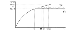
すなわち、まず、(1)図4に示すように、増幅器の温度が上昇し、t1時点において温度がT1(℃)に達したときにオーディオ装置をシャットダウンして出力をオフとし、その後、増幅器の温度が下降し、t2時点において温度がT2(℃)に戻ったときに出力を再開するという動作を繰り返す方法が知られている。 That is, (1) as shown in FIG. 4, when the temperature of the amplifier rises and when the temperature reaches T1 (° C.) at time t1, the audio device is shut down and the output is turned off. There is known a method of repeating the operation of restarting the output when the temperature drops and the temperature returns to T2 (° C.) at time t2.
また、(2)オーディオ装置の温度が所定値以上である状態が所定時間継続したとき、増幅回路の増幅度や、ダイナミックレンジ、出力レベルを制限し、その後、所定温度以下である状態が所定時間継続したとき、これらの制限を解除するようにした方法が知られている(たとえば特許文献1参照)。 Further, (2) when the state where the temperature of the audio device is equal to or higher than a predetermined value continues for a predetermined time, the amplification degree, dynamic range, and output level of the amplifier circuit are limited, and then the state where the temperature is equal to or lower than the predetermined temperature There is known a method in which these restrictions are canceled when it is continued (see, for example, Patent Document 1).
また、(3)増幅器等における温度や電流が所定値以上の場合に音声信号の低域成分や高域成分を中域成分より大きく減衰させるようにした方法が知られている(たとえば特許文献2参照)。 Also, (3) a method is known in which a low frequency component or a high frequency component of an audio signal is attenuated more than a middle frequency component when the temperature or current in an amplifier or the like is a predetermined value or more (for example, Patent Document 2). reference).
また、(4)増幅器への入力信号の振幅を、電源部の温度に基づき、リミッタ回路により制限するようにした方法が知られている(たとえば特許文献3参照)。同文献においては、リミッタ回路内の信号減衰度を非直線的に変化させ、入力信号の振幅が振幅制限値に漸近すると該減衰度を徐々に増加させるソフトリミッタ処理によって波形歪みの発生を低減させ、振幅制限に伴う聴覚上の不自然さを防止することが記載されている(段落0015、0016)。 Further, (4) a method is known in which the amplitude of an input signal to the amplifier is limited by a limiter circuit based on the temperature of the power supply unit (see, for example, Patent Document 3). In this document, the signal attenuation in the limiter circuit is changed nonlinearly, and the occurrence of waveform distortion is reduced by soft limiter processing that gradually increases the attenuation when the amplitude of the input signal approaches the amplitude limit value. , To prevent auditory unnaturalness associated with amplitude limitation (paragraphs 0015 and 0016).
また、(5)増幅器、電源、スピーカ等における温度の変化率に基づいて、増幅器への入力信号の振幅をリミッタ手段により制限する際の制限値の閾値を制御するようにしたものも知られている(たとえば特許文献4参照)。 Also known is (5) a threshold value threshold value for controlling the amplitude of an input signal to an amplifier by a limiter means based on the rate of change of temperature in an amplifier, power supply, speaker, etc. (For example, refer to Patent Document 4).
また、(6)増幅回路の温度等に基づいてオーディオ信号の供給を制限すべきである場合であって、かつ曲間のように入力オーディオ信号のレベルが所定以下である場合にオーディオ信号の供給を制限することにより、聴取者が違和感を覚えることなくオーディオ信号の供給制限を行うようにした技術が知られている(たとえば特許文献5参照)。 Also, (6) supply of an audio signal when the supply of an audio signal should be restricted based on the temperature of the amplifier circuit, etc., and the level of the input audio signal is below a predetermined level, such as between songs There is known a technique for restricting the supply of audio signals without restricting the listener so as to make the listener feel uncomfortable (see, for example, Patent Document 5).
しかしながら、上述(1)の方法によれば、近年のハイパワー化されたオーディオ装置においては、増幅器が小型化、ハイパワー化し、スピーカが低インピーダンス化する傾向にあるので、出力がオフとなる音切れ現象が多発する傾向がある。すなわち、図4に示すように、オーディオ装置は、時点t1において出力をオフとした後、時点t2に至るまで出力を再開しないので、この間において音切れが発生する。これはユーザにとって好ましい動作ではない。 However, according to the above method (1), in a recent high-powered audio apparatus, the amplifier tends to be downsized and high-powered, and the speaker tends to have low impedance. The cutting phenomenon tends to occur frequently. That is, as shown in FIG. 4, since the audio device does not resume output until it reaches time t2 after turning off the output at time t1, a sound break occurs during this time. This is not a preferable operation for the user.
また、上述(2)の方法によれば、音切れはしないが、出力音やダイナミックレンジが小さくなるため、大音量を楽しむユーザに対し、不満を感じさせることになる。また、上述(3)の方法によれば、音切れはしないが、低域信号レベルが減衰されるので、低音域の音量感やパワー感がなくなる。特に、大音量を楽しむウーハアンプのユーザにとっては満足できないものとなる。 Further, according to the method (2), the sound is not cut off, but the output sound and the dynamic range are small, so that the user who enjoys a large volume feels dissatisfied. Further, according to the method (3), the sound is not cut off, but the low-frequency signal level is attenuated, so that there is no sense of volume or power in the low-frequency range. This is particularly unsatisfactory for woofer amp users who enjoy high volume.
また、上述(4)の方法によれば、入力信号の振幅の制限値が一定レベルに設定されるので、振幅の制限が開始されるときに不自然さが生じる。また、上述(5)の方法によれば、リミッタ量が段階的(たとえば10秒毎)に設定されているため、かかる段階的変化が出力音に違和感を生じさせる可能性がある。 Further, according to the above method (4), since the limit value of the amplitude of the input signal is set to a certain level, unnaturalness occurs when the limit of the amplitude is started. Further, according to the method (5) described above, since the limiter amount is set in a stepwise manner (for example, every 10 seconds), such a stepwise change may cause a sense of incongruity in the output sound.
また、上述(6)の方法によれば、オーディオ信号の供給を制限すべきである場合であっても、オーディオ信号に対応する直流信号が第1の閾値未満にならなければ、オーディオ信号の供給が制限されることがないので、その間における発熱等による危険性を回避することができない。また、オーディオ信号の供給が制限された後、オーディオ信号の供給を制限すべき状態が解消し、かつオーディオ信号に対応する直流信号が第1の閾値未満となるまで制限が解除されることがないので、その間、無音状態が続くことになる。 According to the above method (6), even if the supply of the audio signal should be restricted, if the direct-current signal corresponding to the audio signal does not become less than the first threshold value, the supply of the audio signal is performed. Since there is no limitation, it is impossible to avoid danger due to heat generation or the like in the meantime. Further, after the supply of the audio signal is restricted, the state where the supply of the audio signal should be restricted is eliminated, and the restriction is not released until the DC signal corresponding to the audio signal becomes less than the first threshold value. Therefore, the silent state continues during that time.
本発明の目的は、上述従来技術の問題点に鑑み、増幅動作により発生する熱からの保護を、出力音声信号に対して極力悪影響を与えずに行うことができる増幅器の保護回路を提供することにある。 An object of the present invention is to provide an amplifier protection circuit capable of protecting from heat generated by an amplification operation without adversely affecting an output audio signal as much as possible in view of the above-described problems of the prior art. It is in.
この目的を達成するため、第1の発明に係る増幅器の保護回路は、ダイオードの一端に印加される音声信号の振幅が、該ダイオードにおける他端の電圧によって決まる所定の振幅制限値に達する際に該ダイオードが導通することによって、増幅器に入力される前記音声信号の振幅を前記所定の振幅制限値以下となるように制限する振幅制限回路と、前記増幅器の温度に応じて抵抗値が変化する温度検出素子と、前記ダイオードにおける他端の電圧を前記温度検出素子の抵抗値の変化に応じてリアルタイムで連続的に変化させる制御電圧を生成し、前記振幅制限回路に供給することにより前記増幅器の温度が所定の温度制限値以上に上昇するのを防止する温度上昇防止回路とを具備することを特徴とする。 In order to achieve this object, the protection circuit for an amplifier according to the first aspect of the present invention is configured such that when the amplitude of the audio signal applied to one end of the diode reaches a predetermined amplitude limit value determined by the voltage at the other end of the diode. An amplitude limiting circuit that limits the amplitude of the audio signal input to the amplifier to be equal to or lower than the predetermined amplitude limiting value when the diode is turned on; and a temperature at which a resistance value changes according to the temperature of the amplifier The control element generates a control voltage for continuously changing the voltage at the other end of the detection element and the resistance value of the temperature detection element in real time according to a change in the resistance value of the temperature detection element, and supplies the control voltage to the amplitude limiting circuit to And a temperature rise prevention circuit for preventing the temperature from rising above a predetermined temperature limit value.
第2の発明に係る増幅器の保護回路は、第1発明において、前記温度上昇防止回路は、
前記温度検出素子の抵抗値が、前記増幅器の温度が前記温度制限値以上のときの抵抗値である場合に、該抵抗値の変化に応じて変化する電圧を温度検出信号として出力する温度検出回路と、前記温度検出信号に基づいて前記制御電圧を出力する制御回路とを有することを特徴とする。
The amplifier protection circuit according to a second aspect of the present invention is the amplifier according to the first aspect, wherein the temperature rise prevention circuit is
When the resistance value of the temperature detection element is a resistance value when the temperature of the amplifier is equal to or higher than the temperature limit value, a temperature detection circuit that outputs a voltage that changes according to the change of the resistance value as a temperature detection signal And a control circuit that outputs the control voltage based on the temperature detection signal.
第3の発明に係る増幅器の保護回路は、第1又は第2発明において、前記振幅制限回路は、前記増幅器に入力される音声信号がアノードに印加される第1のダイオードと、該音声信号がカソードに印加される第2のダイオードとを備え、前記他端の電圧は、前記第1ダイオードのカソードに印加されるプラス電圧及び前記第2ダイオードのアノードに印加されるマイナス電圧であることを特徴とする。 The amplifier protection circuit according to a third aspect of the present invention is the amplifier circuit according to the first or second aspect, wherein the amplitude limiting circuit includes a first diode to which an audio signal input to the amplifier is applied to an anode, and the audio signal A second diode applied to the cathode, and the voltage at the other end is a positive voltage applied to the cathode of the first diode and a negative voltage applied to the anode of the second diode. And
第4の発明に係る増幅器の保護回路は、第1〜第3のいずれかの発明において、前記制御電圧は前記プラス電圧を変化させるためのプラス側制御電圧及び前記マイナス電圧を変化させるためのマイナス側制御電圧であり、前記振幅制限回路は、所定のプラス電源及びマイナス電源間の電圧を分圧して前記プラス電圧を生成するプラス電圧生成回路と、所定のプラス電源及びマイナス電源間の電圧を分圧して前記マイナス電圧を生成するマイナス電圧生成回路とを備え、前記プラス電圧生成回路は、前記プラス側制御電圧に基づいて前記プラス電圧を下降させる第1の電流制限素子を備え、前記マイナス電圧生成回路は、前記マイナス側制御電圧に基づいて前記マイナス電圧を上昇させる第2の電流制限素子を備えることを特徴とする。 The protection circuit for an amplifier according to a fourth aspect of the present invention is the amplifier protection circuit according to any one of the first to third aspects, wherein the control voltage is a plus side control voltage for changing the plus voltage and a minus side for changing the minus voltage. The amplitude limiting circuit divides a voltage between a predetermined positive power source and a negative power source to generate the positive voltage and a voltage between the predetermined positive power source and the negative power source. A negative voltage generation circuit that generates the negative voltage by pressing, the positive voltage generation circuit including a first current limiting element that lowers the positive voltage based on the positive side control voltage, and generates the negative voltage The circuit includes a second current limiting element that increases the negative voltage based on the negative control voltage.
第5の発明に係る増幅器の保護回路は、第4発明において、前記制御回路は、所定のプラス電源及びマイナス電源間の電圧を分圧して前記プラス側制御電圧を生成する第1の分圧回路と、所定のプラス電源及びマイナス電源間の電圧を分圧して前記マイナス側制御電圧を生成する第2の分圧回路と、前記第1分圧回路及び第2分圧回路間に介在し、前記温度検出信号に応じて前記プラス側制御電圧及びマイナス側制御電圧を変化させる第3の電流制限素子を備えることを特徴とする。 According to a fifth aspect of the present invention, there is provided the amplifier protection circuit according to the fourth aspect, wherein the control circuit divides a voltage between a predetermined positive power source and a negative power source to generate the positive control voltage. A second voltage dividing circuit for dividing the voltage between a predetermined positive power source and a negative power source to generate the negative control voltage, and interposed between the first voltage dividing circuit and the second voltage dividing circuit, A third current limiting element that changes the plus side control voltage and the minus side control voltage according to a temperature detection signal is provided.
第6の発明に係る増幅器の保護回路は、第2〜第5のいずれかの発明において、前記温度検出回路は、前記温度検出素子の抵抗値の変化に応じて変化する電圧を前記温度検出信号として出力する検出信号出力回路と、前記検出信号出力回路からの温度検出信号の出力をオン・オフ制御する第1のスイッチング素子と、前記温度検出素子の抵抗値が、前記増幅器の温度が前記温度制限値以上のときの抵抗値である場合に前記温度検出信号の出力がオン状態となるように前記第1スイッチング素子を制御する第2のスイッチング素子とを有することを特徴とする。 According to a sixth aspect of the present invention, in the amplifier protection circuit according to any one of the second to fifth aspects, the temperature detection circuit generates a voltage that changes according to a change in a resistance value of the temperature detection element. A detection signal output circuit that outputs the temperature detection signal, a first switching element that controls on / off of the output of the temperature detection signal from the detection signal output circuit, a resistance value of the temperature detection element, and a temperature of the amplifier that is the temperature And a second switching element that controls the first switching element so that the output of the temperature detection signal is turned on when the resistance value is equal to or greater than a limit value.
本発明によれば、出力信号に対して極力悪影響を与えることなく、増幅動作により発生する熱から増幅器を保護することができる。 According to the present invention, the amplifier can be protected from heat generated by the amplification operation without adversely affecting the output signal as much as possible.
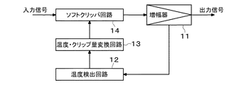
図1は、本発明の一実施形態に係る増幅装置の構成を示すブロック図である。同図に示すようにこの増幅装置は、入力信号を増幅し、増幅装置の出力信号として出力する増幅器11、増幅器11の温度を検出する温度検出回路12、温度検知回路12により検出された温度をクリップ量に変換する温度・クリップ量変換回路13、並びに、温度・クリップ量変換回路13からのクリップ量に基づき、増幅器11への入力信号に対してクリップ処理を施すソフトクリッパ回路14を備える。
FIG. 1 is a block diagram showing a configuration of an amplifying apparatus according to an embodiment of the present invention. As shown in the figure, this amplifying device amplifies an input signal and outputs it as an output signal of the amplifying device, a
ソフトクリッパ回路14は、温度・クリップ量変換回路13から与えられるクリップ量に応じて制限された場合の最大振幅値である振幅制限値を超えないように入力信号の振幅を制限(クリップ)するものである。ただし、本来の信号を振幅制限値で直ちにクリップするのではなく、滑らかに振幅制限値に至るような出力波形に変換するものである。つまり、ソフトクリッパ回路14としては、ダイオードの一端に印加される入力信号の振幅が、該ダイオードにおける他端の電圧によって決まる振幅制限値に達する際に該ダイオードが導通することによって、増幅器11に入力される入力信号の振幅を振幅制限値以下となるように制限するものが用いられる。これによれば、入力電圧が所定値を超えると出力電圧が徐々に立ち上がるダイオードの特性により、急峻なクリップとはならずに滑らかに振幅制限値に達するソフトクリップを行い、不要な高周波成分を低減させることができる。
The
温度検出回路12は、増幅器11の温度に応じて抵抗値が変化するサーミスタ等の温度検出素子を用いて構成され、温度検出素子の抵抗値が、増幅器11の温度が所定の温度制限値Tc以上のときの抵抗値である場合に、該抵抗値の変化に応じて変化する電圧を温度検出信号として、温度・クリップ量変換回路13に供給する。温度・クリップ量変換回路13は、該温度検出信号に基づき、上述のダイオードにおける他端の電圧を該温度検出素子の抵抗値の変化に応じてリアルタイムで連続的に変化させる制御電圧を、クリップ量を表すものとして生成し、ソフトクリッパ回路14に供給する。
The
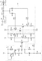
図2は図1の増幅装置の具体例を示す回路図である。図2中の15は入力信号Vinに所定のゲインを付与するオペアンプである。同図に示すように、温度検出回路12は電源端子Vに一端が接続され、増幅器11の温度に応じて抵抗値が変化するサーミスタTH、サーミスタTHの他端にエミッタが接続されたPNPトランジスタTr1、電源端子Vにコレクタが接続され、エミッタがトランジスタTr1のベースに接続されたNPNトランジスタTr2、トランジスタTr2のエミッタ及びグラウンド間に接続された抵抗R1、トランジスタTr1のコレクタに一端が接続された抵抗R2、抵抗R2の他端に一端が接続された抵抗R3、抵抗R3の他端及びグラウンド間に接続された抵抗4、抵抗R3に並列に接続された電界コンデンサC1、並びに、抵抗R3及びR4間の接続点と−15ボルト電源との間に接続された抵抗R5を備える。トランジスタTr2は組込み抵抗を有するデジタルトランジスタであり、組込み抵抗の1つを介してベースが電源端子Vに接続されている。
FIG. 2 is a circuit diagram showing a specific example of the amplifying apparatus of FIG.
クリッパ制御回路(温度・クリップ量変換回路)13は、抵抗R2及びR3間の接続点に一端が接続された抵抗R6、抵抗R6の他端にベースが接続されたNPNトランジスタTr3、トランジスタTr3のコレクタ及び15V電源間に接続された抵抗R7、+15V電源に一端が接続された抵抗R8、抵抗R8の他端及びトランジスタTr3のエミッタ間に接続された抵抗R9、トランジスタTr3のエミッタ及び−15ボルト電源間に接続された抵抗R10、トランジスタTr3のコレクタに一端が接続された抵抗R11、及び抵抗R11の他端及び−15ボルト電源間に接続された抵抗R12を備える。 The clipper control circuit (temperature / clip amount conversion circuit) 13 includes a resistor R6 having one end connected to a connection point between the resistors R2 and R3, an NPN transistor Tr3 having a base connected to the other end of the resistor R6, and a collector of the transistor Tr3. And the resistor R7 connected between the 15V power source, the resistor R8 connected at one end to the + 15V power source, the resistor R9 connected between the other end of the resistor R8 and the emitter of the transistor Tr3, the emitter of the transistor Tr3, and the -15 volt power source , A resistor R11 having one end connected to the collector of the transistor Tr3, and a resistor R12 connected between the other end of the resistor R11 and a −15 volt power source.
ソフトクリッパ回路14は、抵抗R11及びR12間の接続点にベースが接続され、コレクタが−15ボルト電源に接続されたPNPトランジスタTr4、トランジスタTr4のエミッタ及び+15ボルト電源間に接続された抵抗R13、抵抗R8及びR9間の接続点にベースが接続され、コレクタが+15ボルト電源に接続されたNPNトランジスタTr5、トランジスタTr5のエミッタ及び−15ボルト電源間に接続された抵抗R14、トランジスタTr4のエミッタに一端が接続された抵抗R15、抵抗R15の他端にカソードが接続されたダイオードD1、トランジスタTr5のエミッタに一端が接続された抵抗R16、抵抗R16の他端にアノードが接続されたダイオードD2、オペアンプ15の出力端子に一端が接続された抵抗R17、抵抗R17の他端及び増幅器11の入力端子間に接続された抵抗R18を備える。ダイオードD1のアノード及びダイオードD2のカソードはともに抵抗R17及びR18間の接続点に接続されている。
The
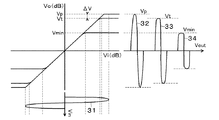
図3は図1の増幅装置の入出力特性を示す。横軸が増幅装置に入力される入力信号VinのレベルViであり、縦軸が増幅装置から出力される出力信号VoutのレベルVoである。なお、図3においては、入力信号Vinの波形及び出力信号Voutの波形例を併せて示している。図中のVtはソフトクリッパ回路14によりソフトクリップ処理がなされる場合の出力信号レベルVoのピーク値(振幅制限値)である。つまり、出力信号Voutにおいてはピーク値Vtを超える部分についてクリップされている。Vp及びVminはピーク値Vtの最大値及び最小値である。すなわちピーク値Vtは、最大ピーク値Vp及び最小ピーク値Vminの間で、温度検出回路12により検出される増幅器11の温度に応じて変化する。ここでは、最大ピーク値Vpとピーク値Vtとの差ΔV(=Vp−Vt)をピーク値がVtである場合のクリップ量という。最大ピーク値Vpは、本来の増幅器電源の実力によるクリップのレベルである。最小ピーク値Vminとしては、クリップによる音量感の変化を感じさせない範囲内での最低のレベルが該当する。
FIG. 3 shows the input / output characteristics of the amplifier of FIG. The horizontal axis is the level Vi of the input signal Vin input to the amplifier, and the vertical axis is the level Vo of the output signal Vout output from the amplifier. Note that FIG. 3 also shows a waveform example of the input signal Vin and a waveform example of the output signal Vout. Vt in the figure is a peak value (amplitude limit value) of the output signal level Vo when soft clip processing is performed by the
図4は増幅器11の温度変化を示すグラフである。横軸は時間t、縦軸は増幅器11の温度Tである。図中の41は時間tに対する増幅器11の温度Tの変化を示すグラフ曲線である。破線42は、ソフトクリッパ回路14に代えて従来の保護回路を適用した場合における増幅器11の温度変化を示すグラフ曲線である。Tmaxは増幅器11において熱によるデバイスの破損を生じさせない温度範囲の最大値である。T1は従来の保護回路において、それ以上増幅器11の温度が上昇するのを防止するために出力をオフ状態とする温度であり、T2は出力をオフ状態とした後、出力を再開するときの温度である。
FIG. 4 is a graph showing the temperature change of the
図2の回路は次のように動作して、上述図3の入出力特性を実現し、図4のグラフ曲線41で示されるような増幅機11の温度変化を達成する。すなわち、動作を開始すると、増幅器11の温度Tが温度制限値Tcを下回っている間は、サーミスタTHの抵抗値は所定値を超えているので、トランジスタTr2はオン状態である。このため、トランジスタTr2のエミッタ電圧V1はトランジスタTr1をオン状態とするまで下降することはなく、トランジスタTr1はオフ状態を維持する。このとき、トランジスタTr3、Tr4及びTr5はオフ状態にあり、トランジスタTr3のコレクタ電圧V3は6[V]、トランジスタTr4のエミッタ電圧は5[V]、トランジスタTr5のベース電圧V5及びエミッタ電圧V6はそれぞれ−6[V]及び−5[V]である。
The circuit of FIG. 2 operates as follows to realize the input / output characteristics of FIG. 3 described above, and achieve the temperature change of the
この後、増幅器11の温度Tが温度制限値Tcに達すると、サーミスタTHの抵抗値は所定値以下となるので、トランジスタTr2はオフ状態となり、電圧V1が低下し、トランジスタTr1がオン状態となる。さらに増幅器11の温度TがTcを超えると、サーミスタTHの抵抗値が減少し、トランジスタTr1のコレクタ電流が増加し、電圧V2が上昇する。すなわち、温度TのTcからの増大量ΔTが、電圧V2の増大量ΔV2となって現れることになる。このようにして温度検出回路12は、増幅器11の温度Tが温度制限値Tc以上の場合に、温度Tに応じた電圧V2を、温度検出信号として出力する。
Thereafter, when the temperature T of the
増幅器11の温度TがTcに達すると、電圧V2によってトランジスタTr3がオン状態となる。この状態において電圧V2がさらに上昇すると、トランジスタTr3のコレクタ電流が増加してコレクタ−エミッタ間電圧が小さくなり、トランジスタTr3のコレクタ電圧V3が+6[V]よりも小さくなるとともに、トランジスタTr5のベース電圧V5が−6[V]よりも大きくなる。この電圧V3は抵抗R11を介してトランジスタTr4のベースに対しプラス側制御電圧として印加される。電圧V5はトランジスタTr5のベースに対しマイナス側制御電圧として印加される。このようにして、クリッパ制御回路13は、増幅器11の温度Tが温度制限値Tc以上の場合に、温度検出回路12からの温度検出信号V2のレベルに応じたレベルの制御電圧をソフトクリッパ回路14に出力する。
When the temperature T of the
電圧V3が+6[V]より小さくなると、トランジスタTr4はオン状態となる。そしてトランジスタTr4の特性に従い、電圧V3の減少分だけ、電圧V4は5[V]よりも小さくなる。同様に、電圧V5が−6[V]より大きくなると、トランジスタTr5はオン状態となる。そして、トランジスタTr5の特性に従い、電圧V5の増加分だけ、電圧V6は−5[V]よりも大きくなる。すなわち、増幅器11の温度Tが温度制限値Tc以上の場合には、ダイオードD1のカソード電圧及びダイオードD2のアノード電圧は、増幅器11の温度Tの増加に応じて減少及び増加する。これに伴い、ダイオードD1及びD2を導通させるダイオードD1及びD2のアノード及びカソード電圧も減少及び増加する。これに応じて、クリップ量ΔVが増加する。このようにして、ソフトクリッパ回路14は、クリッパ制御回路13からの制御電圧に基づき、増幅器11の温度Tが温度制限値Tc以上の場合、増幅器11の温度Tが増加するほど、クリップ量ΔVを増加させ、ピーク値Vtを減少させる。
When the voltage V3 becomes smaller than +6 [V], the transistor Tr4 is turned on. According to the characteristics of the transistor Tr4, the voltage V4 becomes smaller than 5 [V] by the decrease of the voltage V3. Similarly, when the voltage V5 becomes larger than −6 [V], the transistor Tr5 is turned on. Then, according to the characteristics of the transistor Tr5, the voltage V6 becomes larger than −5 [V] by the increase of the voltage V5. That is, when the temperature T of the
これによれば、たとえば図3に示すように、ピークレベルが最大ピーク値Vpである入力信号の波形31が入力された場合、増幅器11の温度Tが温度制限値Tc以下であれば出力信号の波形32のようにクリップされることはないが、増幅器11の温度Tが温度制限値Tcを超えた場合には、波形33のように、温度Tに対応するクリップ量ΔVだけクリップされる。クリップの形態は、ダイオードD1及びD2の特性により、上述のソフトクリップとなる。最大振幅値Vtは温度Tが増加するほど低下し、波形34のように、最小値Vminまで低下することが可能である。最小値Vminは抵抗R15及びR16により決定することができる。
According to this, as shown in FIG. 3, for example, when the
すなわち温度検出回路12、クリッパ制御回路13、及びソフトクリッパ回路14は、増幅器の11の温度が温度制限値Tcを超えて上昇することのないように、増幅器11の温度が温度制限値Tcに達した場合には、増幅器11の温度に基づいてクリップ量ΔVを調整し、増幅器11の温度を温度制限値Tcに維持させるフィードバック制御を行う。
That is, in the
以上説明したように、従来技術によれば、増幅器が所定の温度に達すると、増幅器の入力信号をミュートして出力をオフ状態とし、若しくは増幅器の入力信号レベルをアッテネートし、若しくは入力信号を減衰させ、又は入力信号のレベルを段階的に制限して出力レベルを下げることにより増幅器の温度を下げるようにしていたため、出力信号において音切れや違和感を生じさせていたのに対し、本実施形態によれば、増幅器が所定の温度に達すると、ソフトクリップを掛け始め、その後の温度上昇の度合いに応じて予め設定した深さVminまでのソフトクリップを行うようにしたため、出力信号における音切れや違和感を感じさせることなく、増幅器の温度を一定温度Tcに維持することができる。 As described above, according to the prior art, when the amplifier reaches a predetermined temperature, the amplifier input signal is muted and the output is turned off, or the amplifier input signal level is attenuated or the input signal is attenuated. Or the temperature of the amplifier is lowered by lowering the output level by limiting the level of the input signal step by step. According to this, when the amplifier reaches a predetermined temperature, the soft clip starts to be applied, and the soft clip up to the preset depth Vmin is performed according to the degree of the subsequent temperature rise. The amplifier temperature can be maintained at a constant temperature Tc.
すなわち、増幅器11の温度が温度制限値Tcに達した場合、それ以上の温度の上昇を抑制すべく、増幅器11の温度に基づき、リアルタイムでクリップ量ΔVを制御するようにしたため、音切れを発生することなく、増幅器11の温度が温度制限値Tc以上に上昇するのを防止することができる。
That is, when the temperature of the
また、最小ピーク値Vminを、クリップによる音量感の変化を感じさせないレベルの範囲内で設定するようにしたため、音量感やパワー感をさほど変化させることなく、上記効果を奏することができる。 In addition, since the minimum peak value Vmin is set within a range that does not cause a change in volume feeling due to clipping, the above-described effects can be achieved without changing the volume feeling or power feeling so much.
また、ピーク値を制限するクリップの形態として、ソフトクリップを行うようにしたため、大音量の入力信号の原型を保ちながら、大音量を楽しむユーザに対して音量感の変化や低域におけるパンチ力の劣化をさほど感じさせることなく、上記効果を奏することができる。 In addition, as a form of clip that restricts the peak value, soft clipping is performed, so that while maintaining the original volume of the input signal with a large volume, a change in volume feeling and a punching power at low frequencies can be achieved for users who enjoy a large volume. The above-described effects can be achieved without causing much deterioration.
また、ソフトクリッパ回路14を採用するようにしたため、従来の信号レベルを制限するリミッタ回路において増大する傾向にあり、高域用スピーカであるツイータに対する負荷を増大させ、ツイータの破損を生じさせるおそれのある不要な高周波成分を低減させることができる。
In addition, since the
なお、本発明は上述実施形態に限定されることなく、適宜変形して実施することができる。たとえば、上述においては言及しなかったが、増幅器11における発熱量が多すぎるために、クリップ量ΔVの調整によっては増幅器11の温度を温度制限値Tcに収束させることができず、増幅器11の温度が温度制限値Tcを超えてさらにT1に達した場合には、従来のように増幅装置をシャットダウンするようにしてもよい。
Note that the present invention is not limited to the above-described embodiment, and can be implemented with appropriate modifications. For example, although not mentioned above, since the amount of heat generated in the
また、上述においては、1チャンネルの音声信号を増幅する増幅装置について説明したが、これに限らず、4チャンネルや2チャンネルの音声信号を増幅する増幅装置についても本発明を適用することができる。 In the above description, an amplifying apparatus that amplifies a 1-channel audio signal has been described. However, the present invention is not limited thereto, and the present invention can also be applied to an amplifying apparatus that amplifies 4-channel or 2-channel audio signals.
11:増幅器、12:温度検出回路、13:温度・クリップ量変換回路(クリッパ制御回路)、14:ソフトクリッパ回路、15:オペアンプ、31〜34:波形、41,42:グラフ曲線、C1:電界コンデンサ、D1,D2:ダイオード、R1〜R18:抵抗、Tr1〜Tr5:バイポーラトランジスタ。
11: amplifier, 12: temperature detection circuit, 13: temperature / clip amount conversion circuit (clipper control circuit), 14: soft clipper circuit, 15: operational amplifier, 31-34: waveform, 41, 42: graph curve, C1: electric field Capacitors, D1, D2: diodes, R1-R18: resistors, Tr1-Tr5: bipolar transistors.
Claims (6)
前記増幅器の温度に応じて抵抗値が変化する温度検出素子と、
前記ダイオードにおける他端の電圧を前記温度検出素子の抵抗値の変化に応じてリアルタイムで連続的に変化させる制御電圧を生成し、前記振幅制限回路に供給することにより前記増幅器の温度が所定の温度制限値以上に上昇するのを防止する温度上昇防止回路とを具備することを特徴とする増幅器の保護回路。 When the amplitude of the audio signal applied to one end of the diode reaches a predetermined amplitude limit value determined by the voltage at the other end of the diode, the diode is turned on, whereby the amplitude of the audio signal input to the amplifier is An amplitude limiting circuit that limits the amplitude to be below a predetermined amplitude limit value;
A temperature detecting element whose resistance value changes according to the temperature of the amplifier;
A control voltage for continuously changing the voltage at the other end of the diode in real time according to a change in the resistance value of the temperature detection element is generated and supplied to the amplitude limiting circuit, whereby the temperature of the amplifier is set to a predetermined temperature. An amplifier protection circuit comprising: a temperature rise prevention circuit that prevents the temperature from rising above a limit value.
前記温度検出素子の抵抗値が、前記増幅器の温度が前記温度制限値以上のときの抵抗値である場合に、該抵抗値の変化に応じて変化する電圧を温度検出信号として出力する温度検出回路と、
前記温度検出信号に基づいて前記制御電圧を出力する制御回路とを有することを特徴とする請求項1に記載の増幅器の保護回路。 The temperature rise prevention circuit is
When the resistance value of the temperature detection element is a resistance value when the temperature of the amplifier is equal to or higher than the temperature limit value, a temperature detection circuit that outputs a voltage that changes according to the change of the resistance value as a temperature detection signal When,
The amplifier protection circuit according to claim 1, further comprising a control circuit that outputs the control voltage based on the temperature detection signal.
前記増幅器に入力される音声信号がアノードに印加される第1のダイオードと、
該音声信号がカソードに印加される第2のダイオードとを備え、
前記他端の電圧は、前記第1ダイオードのカソードに印加されるプラス電圧及び前記第2ダイオードのアノードに印加されるマイナス電圧であることを特徴とする請求項1又は2に記載の増幅器の保護回路。 The amplitude limiting circuit includes:
A first diode to which an audio signal input to the amplifier is applied to an anode;
A second diode to which the audio signal is applied to the cathode;
3. The amplifier protection according to claim 1, wherein the voltage at the other end is a positive voltage applied to the cathode of the first diode and a negative voltage applied to the anode of the second diode. circuit.
前記振幅制限回路は、
所定のプラス電源及びマイナス電源間の電圧を分圧して前記プラス電圧を生成するプラス電圧生成回路と、
所定のプラス電源及びマイナス電源間の電圧を分圧して前記マイナス電圧を生成するマイナス電圧生成回路とを備え、
前記プラス電圧生成回路は、前記プラス側制御電圧に基づいて前記プラス電圧を下降させる第1の電流制限素子を備え、
前記マイナス電圧生成回路は、前記マイナス側制御電圧に基づいて前記マイナス電圧を上昇させる第2の電流制限素子を備えることを特徴とする請求項1から3に記載の増幅器の保護回路。 The control voltage is a plus side control voltage for changing the plus voltage and a minus side control voltage for changing the minus voltage,
The amplitude limiting circuit includes:
A positive voltage generation circuit that divides a voltage between a predetermined positive power source and a negative power source to generate the positive voltage;
A negative voltage generating circuit that divides a voltage between a predetermined positive power source and a negative power source to generate the negative voltage;
The plus voltage generation circuit includes a first current limiting element that lowers the plus voltage based on the plus side control voltage;
4. The amplifier protection circuit according to claim 1, wherein the negative voltage generation circuit includes a second current limiting element that increases the negative voltage based on the negative side control voltage. 5.
所定のプラス電源及びマイナス電源間の電圧を分圧して前記プラス側制御電圧を生成する第1の分圧回路と、
所定のプラス電源及びマイナス電源間の電圧を分圧して前記マイナス側制御電圧を生成する第2の分圧回路と、
前記第1分圧回路及び第2分圧回路間に介在し、前記温度検出信号に応じて前記プラス側制御電圧及びマイナス側制御電圧を変化させる第3の電流制限素子を備えることを特徴とする請求項4に記載の増幅器の保護回路。 The control circuit includes:
A first voltage dividing circuit for dividing the voltage between a predetermined plus power source and a minus power source to generate the plus side control voltage;
A second voltage dividing circuit for dividing the voltage between a predetermined positive power source and a negative power source to generate the negative side control voltage;
A third current limiting element is provided between the first voltage dividing circuit and the second voltage dividing circuit, and changes the plus side control voltage and the minus side control voltage according to the temperature detection signal. The protection circuit of the amplifier according to claim 4.
前記検出信号出力回路からの温度検出信号の出力をオン・オフ制御する第1のスイッチング素子と、
前記温度検出素子の抵抗値が、前記増幅器の温度が前記温度制限値以上のときの抵抗値である場合に前記温度検出信号の出力がオン状態となるように前記第1スイッチング素子を制御する第2のスイッチング素子とを有することを特徴とする請求項2〜5のいずれか1項に記載の増幅器の保護回路。 The temperature detection circuit outputs a voltage that changes according to a change in the resistance value of the temperature detection element as the temperature detection signal;
A first switching element for controlling on / off of the output of the temperature detection signal from the detection signal output circuit;
When the resistance value of the temperature detection element is a resistance value when the temperature of the amplifier is equal to or higher than the temperature limit value, the first switching element is controlled to turn on the output of the temperature detection signal. 6. The amplifier protection circuit according to claim 2, comprising two switching elements.
Priority Applications (1)
| Application Number | Priority Date | Filing Date | Title |
|---|---|---|---|
| JP2008316931A JP5109956B2 (en) | 2008-12-12 | 2008-12-12 | Amplifier protection circuit |
Applications Claiming Priority (1)
| Application Number | Priority Date | Filing Date | Title |
|---|---|---|---|
| JP2008316931A JP5109956B2 (en) | 2008-12-12 | 2008-12-12 | Amplifier protection circuit |
Publications (2)
| Publication Number | Publication Date |
|---|---|
| JP2010141682A true JP2010141682A (en) | 2010-06-24 |
| JP5109956B2 JP5109956B2 (en) | 2012-12-26 |
Family
ID=42351401
Family Applications (1)
| Application Number | Title | Priority Date | Filing Date |
|---|---|---|---|
| JP2008316931A Active JP5109956B2 (en) | 2008-12-12 | 2008-12-12 | Amplifier protection circuit |
Country Status (1)
| Country | Link |
|---|---|
| JP (1) | JP5109956B2 (en) |
Cited By (2)
| Publication number | Priority date | Publication date | Assignee | Title |
|---|---|---|---|---|
| US11519786B2 (en) * | 2017-09-25 | 2022-12-06 | Beijing Boe Technology Development Co., Ltd. | Temperature detection circuit, temperature sensor device and display device |
| CN115514329A (en) * | 2022-08-24 | 2022-12-23 | 骏盈半导体(上海)有限公司 | Audio power amplifier circuit and linear over-temperature protection circuit thereof |
Citations (3)
| Publication number | Priority date | Publication date | Assignee | Title |
|---|---|---|---|---|
| JPS5950119U (en) * | 1982-09-25 | 1984-04-03 | ソニー株式会社 | limiter circuit |
| JP2004040258A (en) * | 2002-06-28 | 2004-02-05 | Kenwood Corp | Output limit circuit |
| JP2008236621A (en) * | 2007-03-23 | 2008-10-02 | Toa Corp | Overheat protecting circuit for audio apparatus |
-
2008
- 2008-12-12 JP JP2008316931A patent/JP5109956B2/en active Active
Patent Citations (3)
| Publication number | Priority date | Publication date | Assignee | Title |
|---|---|---|---|---|
| JPS5950119U (en) * | 1982-09-25 | 1984-04-03 | ソニー株式会社 | limiter circuit |
| JP2004040258A (en) * | 2002-06-28 | 2004-02-05 | Kenwood Corp | Output limit circuit |
| JP2008236621A (en) * | 2007-03-23 | 2008-10-02 | Toa Corp | Overheat protecting circuit for audio apparatus |
Cited By (2)
| Publication number | Priority date | Publication date | Assignee | Title |
|---|---|---|---|---|
| US11519786B2 (en) * | 2017-09-25 | 2022-12-06 | Beijing Boe Technology Development Co., Ltd. | Temperature detection circuit, temperature sensor device and display device |
| CN115514329A (en) * | 2022-08-24 | 2022-12-23 | 骏盈半导体(上海)有限公司 | Audio power amplifier circuit and linear over-temperature protection circuit thereof |
Also Published As
| Publication number | Publication date |
|---|---|
| JP5109956B2 (en) | 2012-12-26 |
Similar Documents
| Publication | Publication Date | Title |
|---|---|---|
| JP4178247B2 (en) | Power supply | |
| US9729951B2 (en) | Loudspeaker overload protection | |
| US8582786B2 (en) | Automatic gain control of amplifier by dynamic suppressing and output control at multiple stages | |
| JP2009049671A (en) | Output-limiting circuit, class d power amplifier, sound apparatus | |
| CN102685638B (en) | Method and apparatus for outputting audio signal | |
| KR20070113434A (en) | Input gain automatic control circuit and method | |
| KR101641504B1 (en) | Public address system providing power saving function and speaker protecting function concurrently and power saving circuit used therein | |
| KR20070117171A (en) | Input Gain Limiting Device and Method of Audio Amplifier | |
| JP5109956B2 (en) | Amplifier protection circuit | |
| JP4960734B2 (en) | Overheat protection circuit for audio equipment | |
| JP3296311B2 (en) | Sound equipment | |
| US9634621B1 (en) | Charge-pump power supply with voltage-headroom-dependent supply voltage | |
| JP2016072877A (en) | Power amplifier and power amplification method | |
| JP2016072876A (en) | Power amplification device and power amplification method | |
| US10658988B1 (en) | Open-loop class-D amplifier system with analog supply ramping | |
| JP5303488B2 (en) | Amplitude suppression circuit | |
| US20100097145A1 (en) | Feedback controlled power limiting for signal amplifiers | |
| JP2011155333A (en) | Signal processing circuit | |
| JP2005065124A (en) | hearing aid | |
| JP2013219709A (en) | Voice signal amplification device and television set | |
| TW200937994A (en) | Sound driving circuit for reducing pop noise during powering on and off | |
| JP6891960B2 (en) | Amplifier and its control method | |
| JP2010109845A (en) | Tone control device | |
| JP2010130428A (en) | Output adjusting circuit of power amplifier | |
| JP2005229148A (en) | Power amplifier |
Legal Events
| Date | Code | Title | Description |
|---|---|---|---|
| A621 | Written request for application examination |
Free format text: JAPANESE INTERMEDIATE CODE: A621 Effective date: 20100922 |
|
| A521 | Written amendment |
Free format text: JAPANESE INTERMEDIATE CODE: A523 Effective date: 20110825 |
|
| A711 | Notification of change in applicant |
Free format text: JAPANESE INTERMEDIATE CODE: A712 Effective date: 20111012 |
|
| A977 | Report on retrieval |
Free format text: JAPANESE INTERMEDIATE CODE: A971007 Effective date: 20120214 |
|
| TRDD | Decision of grant or rejection written | ||
| A01 | Written decision to grant a patent or to grant a registration (utility model) |
Free format text: JAPANESE INTERMEDIATE CODE: A01 Effective date: 20120911 |
|
| A01 | Written decision to grant a patent or to grant a registration (utility model) |
Free format text: JAPANESE INTERMEDIATE CODE: A01 |
|
| A61 | First payment of annual fees (during grant procedure) |
Free format text: JAPANESE INTERMEDIATE CODE: A61 Effective date: 20120924 |
|
| FPAY | Renewal fee payment (event date is renewal date of database) |
Free format text: PAYMENT UNTIL: 20151019 Year of fee payment: 3 |
|
| R150 | Certificate of patent or registration of utility model |
Ref document number: 5109956 Country of ref document: JP Free format text: JAPANESE INTERMEDIATE CODE: R150 Free format text: JAPANESE INTERMEDIATE CODE: R150 |