JP2010141569A - Information processor and data transmission method - Google Patents
Information processor and data transmission method Download PDFInfo
- Publication number
- JP2010141569A JP2010141569A JP2008315616A JP2008315616A JP2010141569A JP 2010141569 A JP2010141569 A JP 2010141569A JP 2008315616 A JP2008315616 A JP 2008315616A JP 2008315616 A JP2008315616 A JP 2008315616A JP 2010141569 A JP2010141569 A JP 2010141569A
- Authority
- JP
- Japan
- Prior art keywords
- signal
- information processing
- processing module
- data
- clock
- Prior art date
- Legal status (The legal status is an assumption and is not a legal conclusion. Google has not performed a legal analysis and makes no representation as to the accuracy of the status listed.)
- Withdrawn
Links
Images


Landscapes
- Dc Digital Transmission (AREA)
- Communication Control (AREA)
- Synchronisation In Digital Transmission Systems (AREA)
Abstract
【課題】通信の手順を秘匿することなく、通信データの内容を知得されないようにすること。
【解決手段】信号線により互いに接続された第1の情報処理モジュール及び第2の情報処理モジュールを備え、前記第1の情報処理モジュールは、クロック信号を前記信号線に送出し、及びデータ信号を当該クロック信号の立ち上がりエッジに重畳し、並びに、前記信号線を介して受信したデータ信号に対する送達確認信号を前記クロック信号の立ち下がりエッジに重畳し、前記第2の情報処理モジュールは、前記第1の情報処理モジュールにより前記信号線に送出される前記クロック信号の立ち上がりエッジにデータ信号を重畳し、及び、前記信号線を介して受信したデータ信号に対する送達確認信号を前記クロック信号の立ち下がりエッジに重畳する、情報処理装置を提供する。
【選択図】図8
The content of communication data is prevented from being obtained without concealing the communication procedure.
A first information processing module and a second information processing module are connected to each other by a signal line, the first information processing module sends a clock signal to the signal line, and a data signal. The second information processing module superimposes on the rising edge of the clock signal and superimposes a delivery confirmation signal for the data signal received via the signal line on the falling edge of the clock signal. The data signal is superimposed on the rising edge of the clock signal sent to the signal line by the information processing module, and the delivery confirmation signal for the data signal received via the signal line is set on the falling edge of the clock signal. An information processing apparatus for superimposing is provided.
[Selection] Figure 8
Description
本発明は、情報処理装置及びデータ伝送方法に関する。 The present invention relates to an information processing apparatus and a data transmission method.
一般に、情報技術に関するセキュリティとは、プログラムやデータの機密性、完全性、及び可用性を維持することをいう。その中で、通信におけるセキュリティ上のリスクとしては、例えば、データの盗聴、改竄、又はなりすましなどが挙げられる。また、例えば著作権保護の観点からは、通信経路上を流れるコンテンツデータの不正なコピーなどもセキュリティ上のリスクとなり得る。 In general, security related to information technology refers to maintaining the confidentiality, integrity, and availability of programs and data. Among them, examples of the security risk in communication include data eavesdropping, falsification, or impersonation. Further, for example, from the viewpoint of copyright protection, unauthorized copying of content data flowing on the communication path can be a security risk.
情報通信においてセキュリティを維持するために、多くの場合、暗号化技術が用いられる。例えば、公開鍵暗号方式に基づく電子署名を通信データに付与することで、なりすましやデータの改竄を検知することができる。また、例えば、通信装置間での相互認証を経て通信経路を暗号化することで、通信データを秘匿して盗聴を防止し、又は不正な機器による不法コピーからコンテンツデータを保護することができる。 In order to maintain security in information communication, encryption technology is often used. For example, impersonation or falsification of data can be detected by giving an electronic signature based on a public key cryptosystem to communication data. Further, for example, by encrypting a communication path through mutual authentication between communication devices, it is possible to conceal communication data to prevent eavesdropping, or to protect content data from illegal copying by an unauthorized device.
しかし、仮に通信経路が暗号化されていても、例えば、暗号化された通信データを通信経路のモニタリングにより取得し、取得したデータをなりすましのために転用するという方法で攻撃がなされる場合もある。また、モニタリングにより取得したデータを解析することで、使用されている暗号化アルゴリズムが推測される場合もある。そのため、従来、セキュリティを向上させるためのアプローチとして、通信の手順を秘匿し、及び/又は暗号の強度を高める方向での技術開発が進められていた。 However, even if the communication path is encrypted, an attack may be made by, for example, acquiring encrypted communication data by monitoring the communication path and diverting the acquired data for impersonation. . Moreover, the encryption algorithm currently used may be estimated by analyzing the data acquired by monitoring. Therefore, conventionally, as an approach for improving security, technological development has been advanced in the direction of concealing communication procedures and / or increasing the strength of encryption.
かかる事情は、一般的に、どういった通信技術を用いた場合にも同様である。例えば、下記特許文献1には、機器間でシリアル伝送方式を使用して配線を単純化させることのできる技術が開示されている。下記特許文献1に記載された技術によれば、バイポーラ符号の代表例であるAMI符号を利用してデータが伝送される。このとき、信号レベルの中間値でデータクロックが表現され、受信側で信号レベルに基づいてデータクロックが再生される。
Such a situation is generally the same when any communication technology is used. For example,
しかしながら、通信の手順を秘匿し、又は暗号の強度を高めようとすると、通信処理に要する回路規模や処理量は必然的に増大する。これは、多くの場合に小型化や低消費電力化が求められる通信機器にとってマイナス要因となる。 However, if the communication procedure is concealed or the encryption strength is increased, the circuit scale and processing amount required for the communication processing inevitably increase. This is a negative factor for communication devices that are required to be smaller and consume less power in many cases.
そこで、本発明は、上記問題に鑑みてなされたものであり、本発明の目的とするところは、通信の手順を秘匿することなく、通信データの内容を知得されないようにすることのできる、新規かつ改良された情報処理装置及びデータ伝送方法を提供することにある。 Therefore, the present invention has been made in view of the above problems, and the object of the present invention is to make it impossible to know the contents of communication data without concealing the communication procedure. It is an object of the present invention to provide a new and improved information processing apparatus and data transmission method.
上記課題を解決するために、本発明のある観点によれば、信号線により互いに接続された第1の情報処理モジュール及び第2の情報処理モジュールを備え、前記第1の情報処理モジュールは、クロック信号を前記信号線に送出し、及びデータ信号を当該クロック信号の立ち上がりエッジに重畳し、並びに、前記信号線を介して受信したデータ信号に対する送達確認信号を前記クロック信号の立ち下がりエッジに重畳し、前記第2の情報処理モジュールは、前記第1の情報処理モジュールにより前記信号線に送出される前記クロック信号の立ち上がりエッジにデータ信号を重畳し、及び、前記信号線を介して受信したデータ信号に対する送達確認信号を前記クロック信号の立ち下がりエッジに重畳する、情報処理装置が提供される。 In order to solve the above-described problem, according to an aspect of the present invention, a first information processing module and a second information processing module are connected to each other by a signal line, and the first information processing module includes a clock. A signal is sent to the signal line, a data signal is superimposed on the rising edge of the clock signal, and a delivery confirmation signal for the data signal received via the signal line is superimposed on the falling edge of the clock signal. The second information processing module superimposes a data signal on the rising edge of the clock signal sent to the signal line by the first information processing module, and the data signal received via the signal line An information processing apparatus is provided that superimposes a delivery confirmation signal on the falling edge of the clock signal.
また、前記第1の情報処理モジュール又は前記第2の情報処理モジュールは、送信すべきデータ信号が存在しない任意の時点で、ダミーのデータ信号を前記クロック信号の立ち上がりエッジに重畳してもよい。 Further, the first information processing module or the second information processing module may superimpose a dummy data signal on the rising edge of the clock signal at any time when there is no data signal to be transmitted.
また、前記ダミーのデータ信号は、過去に受信されたデータ信号と同一のビットパターンを有する信号であってもよい。 The dummy data signal may be a signal having the same bit pattern as a data signal received in the past.
また、前記ダミーのデータ信号は、予め定義された所定のビットパターンを有する信号であってもよい。 The dummy data signal may be a signal having a predetermined bit pattern defined in advance.
また、前記第1の情報処理モジュール又は前記第2の情報処理モジュールは、データ信号の衝突を検知していない場合に、連続するデータ信号を所定の時間間隔を空けて前記クロック信号の立ち上がりエッジに重畳可能であってもよい。 In addition, when the first information processing module or the second information processing module does not detect a collision of data signals, the continuous data signal is set to the rising edge of the clock signal with a predetermined time interval. It may be superimposable.
また、前記第1の情報処理モジュールは、前記信号線を用いて前記第2の情報処理モジュールに電力を供給してもよい。 The first information processing module may supply power to the second information processing module using the signal line.
また、前記第1の情報処理モジュール及び前記第2の情報処理モジュールは、データ信号の衝突を検知した場合に、衝突したデータ信号による前記信号線の電圧の変動を打ち消す電圧を有するキャンセル信号を次のクロック信号の立ち上がりエッジに重畳してもよい。 In addition, when the first information processing module and the second information processing module detect a data signal collision, the first information processing module and the second information processing module output a cancel signal having a voltage that cancels a fluctuation in the voltage of the signal line due to the collided data signal. It may be superimposed on the rising edge of the clock signal.
また、前記送達確認信号は、受信されたデータ信号による前記信号線の電圧の変動を打ち消す電圧を有してもよい。 In addition, the delivery confirmation signal may have a voltage that cancels the fluctuation of the voltage of the signal line due to the received data signal.
上記課題を解決するために、本発明の別の観点によれば、信号線を介して互いに接続された第1の情報処理モジュール及び第2の情報処理モジュールを備える情報処理装置において、前記第1の情報処理モジュールにより、クロック信号の立ち上がりエッジにデータ信号を重畳するステップと、前記第1の情報処理モジュールにより、前記クロック信号を前記信号線に送出するステップと、前記第2の情報処理モジュールにより、前記クロック信号に重畳された前記データ信号を受信するステップと、前記第2の情報処理モジュールにより、受信したデータ信号に対する送達確認信号を前記クロック信号の立ち下がりエッジに重畳するステップと、前記第1の情報処理モジュールにより、当該送達確認信号を受信するステップと、を含むデータ伝送方法が提供される。 In order to solve the above problem, according to another aspect of the present invention, in the information processing apparatus including the first information processing module and the second information processing module connected to each other via a signal line, The information processing module superimposes the data signal on the rising edge of the clock signal, the first information processing module sends the clock signal to the signal line, and the second information processing module Receiving the data signal superimposed on the clock signal, superimposing a delivery confirmation signal for the received data signal on the falling edge of the clock signal by the second information processing module, Receiving the delivery confirmation signal by one information processing module. Transmission method is provided.
以上説明したように、本発明に係る情報処理装置及びデータ伝送方法によれば、通信の手順を秘匿することなく、通信データの内容を知得されないようにすることができる。 As described above, according to the information processing apparatus and the data transmission method according to the present invention, it is possible to prevent the contents of communication data from being acquired without concealing the communication procedure.
以下に添付図面を参照しながら、本発明の好適な実施の形態について詳細に説明する。なお、本明細書及び図面において、実質的に同一の機能構成を有する構成要素については、同一の符号を付することにより重複説明を省略する。 Exemplary embodiments of the present invention will be described below in detail with reference to the accompanying drawings. In addition, in this specification and drawing, about the component which has the substantially same function structure, duplication description is abbreviate | omitted by attaching | subjecting the same code | symbol.
また、以下の順序にしたがって当該「発明を実施するための最良の形態」を説明する。
1.本発明に関連する通信方式の説明
1−1.通信方式の概要
1−2.シリアル伝送方式のための構成
2.一実施形態に係る情報処理装置の説明
2−1.情報処理装置の概要
2−2.情報処理装置の構成
2−3.データ信号及び送達確認信号の振幅値
2−4.衝突検知処理
2−5.さらなるセキュリティの向上
3.通信処理の流れの説明
3−1.フローチャート
3−2.信号パターンの例
4.まとめ
The “best mode for carrying out the invention” will be described in the following order.
1. 1. Description of communication method related to the present invention 1-1. Overview of communication method 1-2. 1. Configuration for
<1.本発明に関連する通信方式の説明>
[1−1.通信方式の概要]
まず、図1を参照しながら、本発明に関連する通信方式の概要について説明する。なお、本節で説明する通信方式は、情報処理装置の2つの情報処理モジュールの間で、クロック信号にデータ信号を重畳して通信すると共に、第2の情報処理モジュールにPLL回路を要することなく双方向通信を実現するものである。
<1. Description of Communication System Related to the Present Invention>
[1-1. Overview of communication method]
First, an outline of a communication method related to the present invention will be described with reference to FIG. Note that the communication method described in this section communicates between two information processing modules of an information processing apparatus by superimposing a data signal on a clock signal, and the second information processing module does not require a PLL circuit. It is intended to realize directed communication.
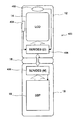
図1は、本発明に関連する通信方式が適用され得る情報処理装置の一例を示す模式図である。図1には、情報処理装置の一例としての携帯端末400が示されている。
FIG. 1 is a schematic diagram showing an example of an information processing apparatus to which a communication method related to the present invention can be applied. FIG. 1 shows a
図1を参照すると、携帯端末400は、主に、表示部12、接続部16、及び操作部18により構成されている。また、表示部12には、撮像部402及び操作スイッチ404が設けられている。
Referring to FIG. 1, the
携帯端末400の表示部12は、液晶ディスプレイなどの画面(図示せず)を有する。そして、表示部12の画面には、例えば、操作部18から表示部12に伝送される任意の画像が表示される。
The
また、表示部12に設けられた撮像部402は、被写体を撮影するためのカメラ機能を提供する。操作スイッチ404は、例えば、撮像部402を用いて被写体を撮影する際のシャッタースイッチとして使用される。また、操作スイッチ404は、例えば、マナーモードへの切り替えなどに使用されてもよい。ここで、例えば、ユーザが操作スイッチ404を操作すると、操作信号が表示部12から操作部18へ伝送される。そして、操作部18から表示部12の撮像部402へ撮影開始命令が出力され、撮像部402による被写体の撮影処理が実行される。その後、撮像部402により撮影された画像データは、表示部12から操作部18へ伝送される。
The
即ち、携帯端末400のような電子機器においては、操作部18(第1の情報処理モジュール)と表示部12(第2の情報処理モジュール)との間で、双方向のデータ伝送が行われる。ここで、例えば2つの情報処理モジュールを接続する接続部16の可動範囲を広げると、その動きにより信号線に損傷が発生する危険性が高まる。そのため、可動部材の自由度、及び信号線の信頼性を両立するために、2つの情報処理モジュールの間の通信方式としてシリアル伝送方式が採用され得る。
That is, in an electronic device such as the
[1−2.シリアル伝送方式のための構成]
図2及び図3を参照しながら、シリアル伝送方式のための装置の構成について説明する。図2は、携帯端末400の全体的な構成を示す説明図である。図3は、携帯端末400の様々な機能の中で双方向通信を実現するためのより詳細な構成について示した説明図である。
[1-2. Configuration for serial transmission system]
The configuration of the apparatus for the serial transmission method will be described with reference to FIGS. FIG. 2 is an explanatory diagram showing the overall configuration of the
(全体的な機能構成)
図2を参照すると、携帯端末400の表示部12には、液晶部14と、撮像部402と、操作スイッチ404と、シリアライザ/デシリアライザ408(SER/DES)とが設けられている。また、携帯端末400の操作部18には、ベースバンドプロセッサ19と、シリアライザ/デシリアライザ406(SER/DES)とが設けられている。なお、以下の説明の中で、操作部18に設けられたシリアライザ/デシリアライザ406をSER/DES(M)と表記することがある。また、表示部12に設けられたシリアライザ/デシリアライザ408をSER/DES(D)と表記することがある。
(Overall functional configuration)
Referring to FIG. 2, the
まず、操作部18から表示部12に向かう信号の流れについて説明する。液晶部14に表示される画像データのパラレル信号は、ベースバンドプロセッサ19により生成される。ベースバンドプロセッサ19により生成されたパラレル信号は、シリアライザ/デシリアライザ406によりシリアル信号に変換される。シリアライザ/デシリアライザ408によりシリアル化された信号は、接続部16を通るシリアル信号線を介して表示部12に設けられたシリアライザ/デシリアライザ408に入力される。シリアライザ/デシリアライザ408は、シリアル信号線を介して入力されたシリアル信号をパラレル信号に変換して液晶部14に入力する。
First, the flow of signals from the
次に、表示部12から操作部18に向かう信号の流れについて説明する。上記の通り、表示部12から操作部18に向かう信号としては、例えば、撮像部402により撮影された画像データの信号や操作スイッチ404により生成された操作信号等がある。ここでは、一例として、撮像部402により撮影された画像データの信号が伝送される場合について説明する。撮像部402から出力されたパラレル信号は、シリアライザ/デシリアライザ408によりシリアル信号に変換され、接続部16を通るシリアル伝送線路を介して操作部18のシリアライザ/デシリアライザ406に入力される。シリアライザ/デシリアライザ406は、シリアル信号線を介して入力されたシリアル信号をパラレル信号に変換し、ベースバンドプロセッサ19に入力する。
Next, the flow of signals from the
上記のような流れで、携帯端末400は、表示部12と操作部18との間における双方向のデータ伝送を実現している。以下、このような双方向通信を実現するためのシリアライザ/デシリアライザ406、408の機能構成について、より詳細に説明する。
With the above-described flow, the
(機能構成の詳細)
図3を参照すると、シリアライザ/デシリアライザ406、408を中心とする携帯端末400の機能構成が示されている。なお、携帯端末400は、信号を直流電源に重畳して伝送する形態を採用している。もちろん、本明細書で説明する技術の適用範囲は、信号を直流電源に重畳して伝送する例に限定されない。
(Details of functional configuration)
Referring to FIG. 3, a functional configuration of the
上記の通り、携帯端末400は、シリアライザ/デシリアライザ406(SER/DES(M))と、シリアライザ/デシリアライザ408(SER/DES(D))とを有する。また、シリアライザ/デシリアライザ406、408は、1本の信号線(例えば、同軸ケーブル等)により接続されている。この信号線は、操作部18から表示部12に直流電源を供給するための電源線としても用いられる。なお、以下の説明においては、SER/DES(M)を単に(M)と表記し、SER/DES(D)を単に(D)と表記する場合がある。
As described above, the
図3に示すように、シリアライザ/デシリアライザ406(M)は、エンコーダ412と、ドライバ414と、合成分配器416と、重畳部418と、レシーバ420と、デコーダ422とを有する。シリアライザ/デシリアライザ408(D)は、分離部432と、合成分配器434と、レシーバ436と、クロック検出部438と、デコーダ440と、バンドパスフィルタ442(BPF)と、エンコーダ444と、ドライバ446とを有する。
As illustrated in FIG. 3, the serializer / deserializer 406 (M) includes an
まず、シリアライザ/デシリアライザ406(M)からシリアライザ/デシリアライザ408(D)にデータ(TX DATA1)を伝送する処理について説明する。 First, processing for transmitting data (TX DATA1) from the serializer / deserializer 406 (M) to the serializer / deserializer 408 (D) will be described.
図3に示すように、シリアライザ/デシリアライザ406(M)には、送信データ(TX DATA1)とクロック信号(TX CLK1)とが入力される。送信データ(TX DATA1)は、エンコーダ412に入力される時点でシリアル化されているものとする。また、クロック信号(TX CLK1)は、エンコーダ412、及びデコーダ422に入力される。送信データ(TX DATA1)及びクロック信号(TX CLK1)が入力されると、エンコーダ412は、まず、ASK(Amplitude Shift Keying)等の所定の変調方式で送信データ(TX DATA1)を符号化されたデータ信号に変換する。そして、エンコーダ412は、データ信号をクロック信号(TX CLK1)に重畳する。なお、データ信号は、例えば振幅変調を応用したAMI(Alternate Mark Inversion)符号により送信データを符号化した信号などであってよい。
As illustrated in FIG. 3, transmission data (TX DATA1) and a clock signal (TX CLK1) are input to the serializer / deserializer 406 (M). It is assumed that the transmission data (TX DATA1) is serialized when it is input to the
エンコーダ412によりデータ信号が重畳されたクロック信号は、ドライバ414を介して合成分配器416に入力される。合成分配器416は、双方向通信を実現するために、エンコーダ412に通じる信号線とデコーダ422に通じる信号線とを分配する。データ送信時には、合成分配器416は、入力された信号を重畳部418に入力する。
The clock signal on which the data signal is superimposed by the
重畳部418では、クロック信号に直流電源が重畳され、重畳信号が生成される。そして、重畳部418により生成された重畳信号は、同軸ケーブルを介してシリアライザ/デシリアライザ408(D)の分離部432に入力される。分離部432は、入力された重畳信号を、直流電源と、データ信号が重畳されたクロック信号とに分離する。分離部432により分離された直流電源は、表示部12に供給される。
In the
一方、分離部432により分離された信号は、合成分配器434に入力される。合成分配器434は、双方向通信を実現するために、デコーダ440に通じる信号線とエンコーダ444に通じる信号線とを分配する手段である。データ受信時の場合には、合成分配器434に入力された信号は、レシーバ436を介してクロック検出部438、及びデコーダ440に入力される。クロック検出部438は、入力された信号からクロックを検出する。このとき、クロック検出部438は、例えば、クロック信号の振幅の極性反転の周期に基づいて、クロック成分を検出することができる。
On the other hand, the signal separated by the
クロック検出部438により検出されたクロックは、例えば液晶部14に供給されると共に、デコーダ440に入力される。デコーダ440は、クロック検出部438から入力されたクロック(RX CLK2)を利用し、入力された信号に復号処理を施して受信データ(RX DATA2)を生成する。このようにしてデコーダ440により生成された受信データ(RX DATA2)は、液晶部14に入力される。
The clock detected by the
以上、シリアライザ/デシリアライザ406(M)からシリアライザ/デシリアライザ408(D)にデータ(TX DATA1)を伝送する処理について説明した。次に、シリアライザ/デシリアライザ408(D)からシリアライザ/デシリアライザ406(M)にデータ(TX DATA2)を伝送する処理について説明する。 The processing for transmitting data (TX DATA1) from the serializer / deserializer 406 (M) to the serializer / deserializer 408 (D) has been described above. Next, processing for transmitting data (TX DATA2) from the serializer / deserializer 408 (D) to the serializer / deserializer 406 (M) will be described.
(SER/DES(D)→SER/DES(M))
既に述べた通り、シリアライザ/デシリアライザ408(D)からシリアライザ/デシリアライザ406(M)にデータ(TX DATA2)を伝送するためには、シリアライザ/デシリアライザ408(D)の側でクロックが必要になる。しかしながら、クロック信号を生成するためにシリアライザ/デシリアライザ408(D)の側にPLL(Phase-Locked Loop)回路を設けると、消費電力が大きくなってしまう。
(SER / DES (D) → SER / DES (M))
As described above, in order to transmit data (TX DATA2) from the serializer / deserializer 408 (D) to the serializer / deserializer 406 (M), a clock is required on the serializer / deserializer 408 (D) side. However, if a PLL (Phase-Locked Loop) circuit is provided on the serializer / deserializer 408 (D) side in order to generate a clock signal, power consumption increases.
そこで、シリアライザ/デシリアライザ406(M)からシリアライザ/デシリアライザ408(D)にクロック信号が供給されるように工夫が施される。シリアライザ/デシリアライザ406(M)は、例えば、自身がデータを送信しない時間帯であっても、クロック信号をシリアライザ/デシリアライザ408(D)に伝送し続ける。そして、シリアライザ/デシリアライザ408(D)は、データを伝送する際、シリアライザ/デシリアライザ406(M)から受信したクロック信号にデータ信号を重畳してデータを伝送する。シリアライザ/デシリアライザ406(M)から送信されたクロック信号は、分離部432、合成分配器434、レシーバ436を介してクロック検出部438に入力される。そこで、クロック検出部438は、入力された信号からクロック信号を検出し、バンドパスフィルタ442に入力する。通常、クロック検出部438により検出されたクロック信号には、ジッタが多く含まれている。そのため、クロック検出部438により検出されたクロック信号は、バンドパスフィルタ442によって、ジッタを抑圧される。
Therefore, a contrivance is made so that a clock signal is supplied from the serializer / deserializer 406 (M) to the serializer / deserializer 408 (D). For example, the serializer / deserializer 406 (M) continues to transmit the clock signal to the serializer / deserializer 408 (D) even in a time zone in which the serializer / deserializer 406 (M) does not transmit data. The serializer / deserializer 408 (D) transmits data by superimposing the data signal on the clock signal received from the serializer / deserializer 406 (M) when transmitting data. The clock signal transmitted from the serializer / deserializer 406 (M) is input to the
バンドパスフィルタ442によりジッタが抑圧されたクロック信号は、エンコーダ444に入力される。また、エンコーダ444には、送信データ(TX DATA2)が入力される。そうすると、エンコーダ444は、ASK等の所定の変調方式で送信データ(TX DATA2)を符号化されたデータ信号に変換する。そして、エンコーダ444により符号化されたデータ信号は、クロック信号に合わせて、ドライバ446を介して合成分配器434に入力される。合成分配器434は、エンコーダ444から入力されるデータ信号をシリアライザ/デシリアライザ406(M)から伝送されたクロック信号に重畳して重畳信号を生成する。そして、重畳信号は、分離部432を介して同軸ケーブルに送出され、シリアライザ/デシリアライザ406(M)に伝送される。
The clock signal whose jitter is suppressed by the
シリアライザ/デシリアライザ406(M)においては、同軸ケーブルを通じて伝送された重畳信号が、重畳部418、合成分配器416、レシーバ420を介してデコーダ422に入力される。デコーダ422は、符号が振幅変調されている場合には、入力された符号の振幅値に基づいてデータを復号する。このとき、デコーダ422は、送信データ(TX DATA1)の送信に用いるクロック信号(TX CLK1)を用いてデータを復号する。
In the serializer / deserializer 406 (M), the superimposed signal transmitted through the coaxial cable is input to the
なお、シリアライザ/デシリアライザ408(D)がデータ伝送に用いたクロックは、シリアライザ/デシリアライザ406(M)から伝送された送信用クロック(TX CLK1)である。そのため、デコーダ422は、入力された符号からクロックを検出する必要がない。デコーダ422により復号されたデータ(RX DATA1)、及びクロック(RX CLK1)は、ベースバンドプロセッサ19に入力される。
Note that the clock used by the serializer / deserializer 408 (D) for data transmission is the transmission clock (TX CLK1) transmitted from the serializer / deserializer 406 (M). Therefore, the
以上、シリアライザ/デシリアライザ408(D)からシリアライザ/デシリアライザ406(M)にデータ(TX DATA2)を伝送する処理について説明した。このようにして、PLLを用いることなく、シリアライザ/デシリアライザ408(D)からシリアライザ/デシリアライザ406(M)へのデータ伝送が実現される。 The processing for transmitting data (TX DATA2) from the serializer / deserializer 408 (D) to the serializer / deserializer 406 (M) has been described above. In this way, data transmission from the serializer / deserializer 408 (D) to the serializer / deserializer 406 (M) is realized without using a PLL.
[1−3.シリアル伝送方式における課題]
上述したシリアル伝送方式では、双方向の通信で1つの信号線が共有されるため、信号の衝突を回避する仕組み、又は信号の衝突を検知して信号を再送可能とする仕組みが必要となる。そこで、例えば、時分割伝送(TDD;Time Division Duplex)方式を採用し、順方向の伝送と逆方向の伝送とでタイムスロットを分けることも考えられる。しかし、時分割伝送方式を採用した場合には、タイムスロットの定義が不正なユーザ又は第三者(以下、悪意のある第三者を含めて、不正ユーザと総称する)に知得されると、通信データの内容を容易に読み取られてしまう可能性がある。また、通信データを秘匿するためにデータを暗号化しようとすると、追加的な暗号化/復号処理が必要となり、回路規模の増加や消費電力の増大などのデメリットが生じる。これにたいし、次節より詳しく説明する本発明の一実施形態に係る新たな伝送方式によれば、情報処理モジュール間の通信のセキュリティを向上させることができる。
[1-3. Issues in serial transmission system]
In the serial transmission method described above, since one signal line is shared in two-way communication, a mechanism for avoiding signal collision or a mechanism for detecting a signal collision and enabling signal retransmission is required. Thus, for example, a time division transmission (TDD) method may be adopted to divide the time slots into forward transmission and reverse transmission. However, when the time division transmission method is adopted, the definition of the time slot is known to an unauthorized user or a third party (hereinafter collectively referred to as an unauthorized user including a malicious third party). The content of communication data may be easily read. In addition, if the data is to be encrypted in order to keep the communication data confidential, additional encryption / decryption processing is required, resulting in disadvantages such as an increase in circuit scale and power consumption. On the other hand, according to the new transmission method according to the embodiment of the present invention described in detail in the next section, it is possible to improve the security of communication between the information processing modules.
<2.一実施形態に係る情報処理装置の説明>
[2−1.情報処理装置の概要]
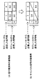
まず、図4を用いて、本発明の一実施形態に係る情報処理装置の概要について説明する。図4は、一実施形態に係る情報処理装置100について概略的に示す模式図である。図4を参照すると、情報処理装置100の2つの例(情報処理装置100a及び100b)が示されている。
<2. Description of Information Processing Apparatus According to One Embodiment>
[2-1. Overview of information processing equipment]
First, an outline of an information processing apparatus according to an embodiment of the present invention will be described with reference to FIG. FIG. 4 is a schematic diagram schematically illustrating the
情報処理装置100aは、例えば図1を用いて説明した携帯電話400と同様の端末装置である。情報処理装置100aは、接続部103aにより互いに接続される操作部102a及び表示部104aを備える(図4(A)参照)。情報処理装置100aにおいて、操作部102a及び表示部104aはそれぞれ内部にプロセッサとしての半導体チップ(図示せず)を有し、接続部103aに設けられる信号線(図示せず)を介してシリアル伝送方式で双方向通信する。
The
一方、情報処理装置100bは、それぞれ別体に構成され、信号線103bにより互いに接続される記録モジュール102b及び表示モジュール104bを備える記録再生装置である(図4(B)参照)。情報処理装置100bにおいて、記録モジュール102b及び表示モジュール104bはそれぞれ内部にプロセッサとしての半導体チップ(図示せず)を有し、信号線103bを介してシリアル伝送方式で双方向通信する。
On the other hand, the
なお、本実施形態に係る情報処理装置100は、図4に例示した端末装置又は記録再生装置に限定されない。情報処理装置100は、2つの情報処理モジュール間でシリアル伝送方式で双方向通信する任意の装置であってよい。また、本明細書において、情報処理装置100aと情報処理装置100bとを区別する必要がない場合には、情報処理装置100と総称する。同様に、本明細書において、図4に例示した操作部102a及び記録モジュール102bを第1の情報処理モジュール102、表示部104a及び表示モジュール104bを第2の情報処理モジュール104と総称する。
Note that the
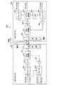
[2−2.情報処理装置の構成]
次に、図5を用いて、情報処理装置100の構成の一例を説明する。図5は、情報処理装置100の様々な機能の中で、双方向通信を実現するためのより詳細な構成について示す説明図である。
[2-2. Configuration of information processing apparatus]
Next, an example of the configuration of the
図5を参照すると、第1の情報処理モジュール102が有するシリアライザ/デシリアライザ106、及び第2の情報処理モジュール104が有するシリアライザ/デシリアライザ108を中心とする情報処理装置100の構成が示されている。
Referring to FIG. 5, the configuration of the
シリアライザ/デシリアライザ106及び108は、信号線(例えば、同軸ケーブル等)により相互に接続される。この信号線は、第1の情報処理モジュール102から第2の情報処理モジュール104に直流電源を供給するための電源線としても用いられ得る。また、シリアライザ/デシリアライザ106及び108は、信号線の電圧を測定する際の基準電圧を供給する接地線(GND)によりさらに接続され得る。
The serializer /
図5に示すように、シリアライザ/デシリアライザ106(M)は、エンコーダ112、ドライバ114、合成分配器116、重畳部118、レシーバ120、及びデコーダ122を有する。また、エンコーダ112には、送信制御部128が含まれる。さらに、デコーダ122には、送達確認部124、及び衝突検知部126が含まれる。一方、シリアライザ/デシリアライザ108(D)は、分離部132、合成分配器134、レシーバ136、クロック検出部138、デコーダ140、バンドパスフィルタ142、エンコーダ144、及びドライバ146を有する。また、エンコーダ144には、送信制御部152が含まれる。さらに、デコーダ140には、送達確認部148及び衝突検知部150が含まれる。
As illustrated in FIG. 5, the serializer / deserializer 106 (M) includes an
本実施形態に係る情報処理装置100と図3に示した携帯電話400との間の主な相違点の1つは、第1の情報処理モジュール102の構成に、送達確認部124、衝突検知部126、及び送信制御部128が追加されている点である。同様に、第2の情報処理モジュール104の構成には、送達確認部148、衝突検知部150、及び送信制御部152が追加されている。なお、追加された各処理ブロックは、例えば、エンコーダ112若しくはデコーダ122、又はエンコーダ144若しくはデコーダ140から独立して構成されてもよい。次に、かかる情報処理装置100の構成において、第1の情報処理モジュール102と第2の情報処理モジュール104との間で送受信される信号の流れについて説明する。
One of the main differences between the
[2−2−1.信号の流れ(SER/DES(M)→SER/DES(D))]
図3の例と同様、シリアライザ/デシリアライザ106(M)には、送信データ(TX DATA1)とクロック信号(TX CLK1)とが入力される。送信データ(TX DATA1)は、エンコーダ112に入力される時点でシリアル化されているものとする。また、クロック信号(TX CLK1)は、エンコーダ112、及びデコーダ122に入力される。送信データ(TX DATA1)及びクロック信号(TX CLK1)が入力されると、エンコーダ112は、まず、送信データ(TX DATA1)を、後にさらに詳しく説明する特別な振幅値に変調されたデータ信号に変換する。そして、エンコーダ112は、データ信号をクロック信号(TX CLK1)の立ち上がりエッジに重畳する。
[2-2-1. Signal flow (SER / DES (M) → SER / DES (D))]
Similar to the example of FIG. 3, the transmission data (TX DATA1) and the clock signal (TX CLK1) are input to the serializer / deserializer 106 (M). It is assumed that the transmission data (TX DATA1) is serialized when it is input to the
エンコーダ112によりデータ信号が重畳されたクロック信号は、ドライバ114を介して合成分配器116に入力される。合成分配器116は、双方向通信を実現するために、エンコーダ112に通じる信号線とデコーダ122に通じる信号線とを分配する。データ送信時には、合成分配器116は、入力された信号を重畳部118に入力する。
The clock signal on which the data signal is superimposed by the
また、本実施形態では、エンコーダ112は、データ信号をクロック信号に重畳した後、デコーダ122の衝突検知部126にデータ信号を出力したことを通知する。そうすると、衝突検知部126は、第2の情報処理モジュール104から返信される信号を監視し、信号の衝突が生じた場合にはその衝突を検知する。衝突検知部126による衝突検知処理については、後にさらに説明する。
In this embodiment, the
重畳部118では、クロック信号に直流電源が重畳され、重畳信号が生成される。そして、重畳部118により生成された重畳信号は、例えば同軸ケーブルを介してシリアライザ/デシリアライザ108(D)の分離部132に入力される。分離部132は、入力された重畳信号を、直流電源と、データ信号が重畳されたクロック信号とに分離する。分離部132により分離された直流電源は、第2の情報処理モジュール104に供給される。
The superimposing
一方、分離部132により分離された信号は、合成分配器134に入力される。合成分配器134は、双方向通信を実現するために、デコーダ140に通じる信号線とエンコーダ144に通じる信号線とを分配する手段である。データ受信時の場合には、合成分配器134に入力された信号は、レシーバ136を介してクロック検出部138、及びデコーダ140に入力される。クロック検出部138は、入力された信号からクロックを検出する。このとき、クロック検出部138は、例えば、信号の直流成分を除いた場合の振幅値極性反転の周期に基づいて、クロック成分を検出することができる。
On the other hand, the signal separated by the
クロック検出部138により検出されたクロックは、デコーダ140及びバンドパスフィルタ142に入力される。デコーダ140は、クロック検出部138からのクロック(RX CLK2)の立ち上がりエッジに合わせて、入力された信号に復号処理を施して受信データ(RX DATA2)を生成する。デコーダ140により生成された受信データ(RX DATA2)は、第2の情報処理モジュール104の制御部(図示せず)等に入力される。また、デコーダ140の送達確認部148は、エンコーダ144を介して、受信データ(RX DATA2)の信号値に応じた送達確認信号をクロック検出部138からのクロック(RX CLK2)の立ち下がりエッジに合わせて送信する。送達確認部148により送信される送達確認信号については、後にさらに説明する。
The clock detected by the
以上、シリアライザ/デシリアライザ106(M)からシリアライザ/デシリアライザ108(D)にデータ(TX DATA1)を伝送する処理について説明した。次に、シリアライザ/デシリアライザ108(D)からシリアライザ/デシリアライザ106(M)にデータ(TX DATA2)を伝送する処理について説明する。 The processing for transmitting data (TX DATA1) from the serializer / deserializer 106 (M) to the serializer / deserializer 108 (D) has been described above. Next, processing for transmitting data (TX DATA2) from the serializer / deserializer 108 (D) to the serializer / deserializer 106 (M) will be described.
[2−2−2.信号の流れ(SER/DES(D)→SER/DES(M))]
図3の例と同様、シリアライザ/デシリアライザ106(M)は、自身がデータを送信しない場合であっても、クロック信号をシリアライザ/デシリアライザ108(D)に伝送し続ける。そして、シリアライザ/デシリアライザ108(D)は、データを伝送する際、シリアライザ/デシリアライザ106(M)から受信したクロック信号にデータ信号を重畳してデータを伝送する。シリアライザ/デシリアライザ106(M)から送信されたクロック信号は、分離部132、合成分配器134、レシーバ136を介してクロック検出部138に入力される。クロック検出部138は、入力された信号からクロック信号を検出し、ジッタを抑圧するためにバンドパスフィルタ142に入力する。
[2-2-2. Signal flow (SER / DES (D) → SER / DES (M))]
Similar to the example of FIG. 3, the serializer / deserializer 106 (M) continues to transmit the clock signal to the serializer / deserializer 108 (D) even when it does not transmit data. Then, when transmitting data, the serializer / deserializer 108 (D) transmits data by superimposing the data signal on the clock signal received from the serializer / deserializer 106 (M). The clock signal transmitted from the serializer / deserializer 106 (M) is input to the
バンドパスフィルタ142によりジッタが抑圧されたクロック信号は、エンコーダ144に入力される。また、エンコーダ144には、送信データ(TX DATA2)が入力される。そうすると、エンコーダ144は、送信データ(TX DATA2)を、後にさらに詳しく説明する特別な振幅値に変調されたデータ信号に変換する。そして、エンコーダ144により符号化されたデータ信号は、クロック信号の立ち上がりエッジに合わせて、ドライバ146を介して合成分配器134に入力される。合成分配器134は、エンコーダ144から入力されるデータ信号をシリアライザ/デシリアライザ106(M)から伝送されたクロック信号の立ち上がりエッジに重畳して重畳信号を生成する。そして、重畳信号は、分離部132を介して同軸ケーブルに送出され、シリアライザ/デシリアライザ106(M)に伝送される。
The clock signal whose jitter is suppressed by the
さらに、本実施形態では、エンコーダ144は、データ信号をクロック信号に重畳した後、デコーダ140の衝突検知部150にデータ信号を出力したことを通知する。そうすると、衝突検知部150は、第1の情報処理モジュール102から返信される信号を監視し、信号の衝突が生じた場合にはその衝突を検知する。衝突検知部150による衝突検知処理については、後にさらに説明する。
Furthermore, in this embodiment, the
シリアライザ/デシリアライザ106(M)においては、同軸ケーブルを通じて伝送された重畳信号が、重畳部118、合成分配器116、レシーバ120を介してデコーダ122に入力される。デコーダ122は、入力された符号の振幅値に基づいてデータを復号する。このとき、デコーダ122は、送信データ(TX DATA1)の送信に用いるクロック信号(TX CLK1)を用いてデータを復号する。
In the serializer / deserializer 106 (M), the superimposed signal transmitted through the coaxial cable is input to the
なお、シリアライザ/デシリアライザ108(D)がデータ伝送に用いたクロックは、シリアライザ/デシリアライザ106(M)から伝送された送信用クロック(TX CLK1)である。そのため、デコーダ122は、入力された符号からクロックを検出する必要がない。デコーダ122により復号されたデータ(RX DATA1)、及びクロック(RX CLK1)は、第1の情報処理モジュール102の制御部(図示せず)等に入力される。また、デコーダ122の送達確認部124は、エンコーダ112を介して、受信データ(RX DATA1)の信号値に応じた送達確認信号をクロック(TX CLK1)の立ち下がりエッジに合わせて送信する。送達確認部124により送信される送達確認信号については、後にさらに説明する。
Note that the clock used by the serializer / deserializer 108 (D) for data transmission is the transmission clock (TX CLK1) transmitted from the serializer / deserializer 106 (M). Therefore, the
以上、シリアライザ/デシリアライザ108(D)からシリアライザ/デシリアライザ106(M)にデータ(TX DATA2)を伝送する処理について説明した。次に、本実施形態において、シリアライザ/デシリアライザ106(M)とシリアライザ/デシリアライザ108(D)との間で送受信されるクロック信号に重畳されるデータ信号及び送達確認信号の振幅値について説明する。 The processing for transmitting data (TX DATA2) from the serializer / deserializer 108 (D) to the serializer / deserializer 106 (M) has been described above. Next, in this embodiment, the amplitude value of the data signal and the delivery confirmation signal superimposed on the clock signal transmitted / received between the serializer / deserializer 106 (M) and the serializer / deserializer 108 (D) will be described.
[2−3.データ信号及び送達確認信号の振幅値]
図6は、データ信号と送達確認信号の振幅値の一例について説明するための説明図である。
[2-3. Amplitude values of data signal and delivery confirmation signal]
FIG. 6 is an explanatory diagram for explaining an example of amplitude values of the data signal and the delivery confirmation signal.
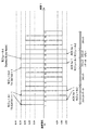
図6を参照すると、クロック信号、データ信号、及び送達確認信号の3種類の信号について、基準電圧(直流成分の電圧)を5.0Vとした場合の信号値ごとの振幅値の一例が示されている。また、図6には、各信号がクロック信号の立ち上がりエッジと立ち下がりエッジのどちらに重畳されるかも示されている。 Referring to FIG. 6, an example of an amplitude value for each signal value when the reference voltage (DC component voltage) is 5.0 V is shown for three types of signals, a clock signal, a data signal, and an acknowledgment signal. ing. FIG. 6 also shows whether each signal is superimposed on the rising edge or falling edge of the clock signal.
まず、クロック信号については、特に信号値は規定されない。クロック信号は、その立ち上がりエッジにおいて基準電圧から1.0V高い6.0Vとなり、その立ち下がりエッジにおいて基準電圧から1.0V低い4.0Vとなる。なお、ここでのクロック信号の振幅値は、データ信号が重畳されていない状態での振幅値である。 First, a signal value is not specified for the clock signal. The clock signal becomes 6.0V, which is 1.0V higher than the reference voltage at the rising edge, and becomes 4.0V which is 1.0V lower than the reference voltage at the falling edge. The amplitude value of the clock signal here is an amplitude value in a state where the data signal is not superimposed.
次に、データ信号は、“1”及び“0”のいずれの信号値についても、クロック信号の立ち上がりエッジに重畳される。このとき、信号値“1”のデータ信号の振幅値を、クロック信号の立ち上がりエッジの振幅値6.0Vにさらにシフト値0.2Vを重畳し、6.2Vとする。これに対し、信号値“0”のデータ信号の振幅値を、クロック信号の立ち上がりエッジの振幅値6.0Vにさらに正負の反転したシフト値−0.2Vを重畳し、5.8Vとする。このようなクロック信号に重畳されたデータ信号は、第1の情報処理モジュール102のデコーダ122、又は第2の情報処理モジュール104のデコーダ140の内部に設けられるコンパレータにおいて予め与えられる振幅の閾値と比較され、各信号値に復号される。
Next, the data signal is superimposed on the rising edge of the clock signal for both “1” and “0” signal values. At this time, the amplitude value of the data signal with the signal value “1” is set to 6.2 V by further superimposing the shift value 0.2 V on the amplitude value 6.0 V of the rising edge of the clock signal. On the other hand, the amplitude value of the data signal with the signal value “0” is superimposed on the amplitude value 6.0V of the rising edge of the clock signal and a shift value −0.2V, which is inverted from positive to negative, to be 5.8V. The data signal superimposed on such a clock signal is compared with an amplitude threshold given in advance in a comparator provided in the
一方、送達確認信号は、“1”及び“0”のいずれの信号値に対する送達確認信号の場合にも、クロック信号の立ち下がりエッジに重畳される。このとき、信号値“1”のデータ信号に対する送達確認信号の振幅値を、クロック信号の立ち下がりエッジの振幅値4.0Vに正負の反転したシフト値−0.2Vを重畳し、3.8Vとする。同様に、信号値“0”のデータ信号に対する送達確認信号の振幅値を、クロック信号の立ち下がりエッジの振幅値4.0Vにシフト値0.2Vを重畳し、4.2Vとする。このような送達確認信号の送信(振幅値の制御)は、例えば、データ信号を受信したいずれかの情報処理モジュールの送達確認部124又は148により、エンコーダ112又は144を介して行われる。それにより、データ信号を送信した情報処理モジュールは、送信した信号値が正しく相手側のモジュールに送達したことを知ることができる。また、データ信号として“1”又は“0”のいずれの信号値が送信された場合でも、データ信号による信号線の電圧の変動が送達確認信号によってキャンセルされる(振幅値の平均が基準電圧に等しくなる)ため、信号の直流成分が変動することが防がれる。
On the other hand, the delivery confirmation signal is superimposed on the falling edge of the clock signal in the case of the delivery confirmation signal for any signal value of “1” and “0”. At this time, the amplitude value of the delivery confirmation signal with respect to the data signal having the signal value “1” is superimposed on the amplitude value 4.0V of the falling edge of the clock signal by superimposing a positive / negative inverted shift value −0.2V to obtain 3.8V. And Similarly, the amplitude value of the delivery confirmation signal for the data signal having the signal value “0” is set to 4.2 V by superimposing the shift value 0.2 V on the amplitude value 4.0 V of the falling edge of the clock signal. Transmission of such a delivery confirmation signal (amplitude value control) is performed via the
[2−4.衝突検知処理]
図6に示した振幅値でデータ信号をクロック信号に重畳させて送信する場合にも、第1の情報処理モジュール102と第2の情報処理モジュール104が同時に信号を送信すると、クロック信号の立ち上がりエッジにおいて信号の衝突が発生して通信は失敗する。そこで、本実施形態では、第1の情報処理モジュール102の衝突検知部126及び第2の情報処理モジュール104の衝突検知部150により、信号の衝突を検知する。
[2-4. Collision detection process]
Even when the data signal is transmitted with the amplitude value shown in FIG. 6 superimposed on the clock signal, if the first information processing module 102 and the second information processing module 104 transmit signals simultaneously, the rising edge of the clock signal is transmitted. In this case, a signal collision occurs and communication fails. Therefore, in the present embodiment, signal collision is detected by the
図7は、第1の情報処理モジュール102の衝突検知部126及び第2の情報処理モジュール104の衝突検知部150による衝突検知処理について説明するための説明図である。なお、ここでは、クロック信号に重畳されたデータ信号が図6を用いて説明した振幅値をとるという前提のもとに説明を行う。
FIG. 7 is an explanatory diagram for explaining the collision detection processing by the
図7(A)を参照すると、信号の衝突が発生した際の信号の振幅値が、各モジュールから送信されたデータ信号の信号値の組合せごとに示されている。例えば、両方のモジュールから同時に信号値“1”が送信された場合、信号の振幅値(信号線の電圧)は、クロック信号の電圧値6.0Vに2つのモジュール分のシフト値(0.2V×2=0.4V)を加え、6.4Vとなる。また、例えば、一方のモジュールから信号値“1”、他方のモジュールから信号値“0”が送信された場合、信号の振幅値は、クロック信号の電圧値6.0Vにシフト値0.2Vと−0.2Vを加え、6.0Vとなる。また、例えば、両方のモジュールから同時に信号値“0”が送信された場合、信号の振幅値は、クロック信号の電圧値6.0Vに2つのモジュール分のシフト値(−0.2V×2=−0.4V)を加え、5.6Vとなる。 Referring to FIG. 7A, the amplitude value of a signal when a signal collision occurs is shown for each combination of signal values of a data signal transmitted from each module. For example, when the signal value “1” is transmitted simultaneously from both modules, the signal amplitude value (signal line voltage) is shifted to the voltage value 6.0 V of the clock signal by two modules (0.2 V). X2 = 0.4V) is added to obtain 6.4V. For example, when a signal value “1” is transmitted from one module and a signal value “0” is transmitted from the other module, the amplitude value of the signal is changed to a voltage value 6.0 V of the clock signal and a shift value 0.2 V. -0.2V is added and it becomes 6.0V. Also, for example, when the signal value “0” is transmitted from both modules simultaneously, the amplitude value of the signal is shifted to the voltage value 6.0 V of the clock signal (−0.2 V × 2 = -0.4V) is added to 5.6V.
即ち、信号の衝突が発生した場合には、衝突が発生していない場合のデータ信号の振幅値6.2V又は5.8Vとは必ず異なる値となる。これを利用し、第1の情報処理モジュール102の衝突検知部126及び第2の情報処理モジュール104の衝突検知部150は、受信した信号の振幅値を所定の閾値と比較するコンパレータを用いて判定して、信号の衝突の発生を検知する。
That is, when a signal collision occurs, the amplitude value of the data signal when the collision does not occur is always different from 6.2V or 5.8V. Using this, the
さらに、衝突検知部126及び衝突検知部150は、信号の衝突を検知すると、衝突による信号線の電圧の変動を打ち消す電圧を有するキャンセル信号を、エンコーダ112又はエンコーダ144を介して、次のクロック信号の立ち上がりエッジに重畳する。
Further, when the
図7(B)を参照すると、信号の衝突による電圧の変動を打ち消すキャンセル信号の振幅値が、各モジュールから送信されたデータ信号の信号値の組合せごとに示されている。例えば、両方のモジュールから同時に信号値“1”が送信された場合には、信号の衝突による電圧の変動は0.4Vであるため、キャンセル信号の振幅値を6.0V−0.4V=5.6Vとする必要がある。そこで、シフト値−0.2Vをクロック信号に重畳させたキャンセル信号を両方のモジュールから送信することにより、信号線の電圧を5.6Vとする。 Referring to FIG. 7B, the amplitude value of the cancel signal that cancels the voltage fluctuation caused by the signal collision is shown for each combination of the signal values of the data signal transmitted from each module. For example, when the signal value “1” is transmitted from both modules at the same time, the voltage fluctuation due to signal collision is 0.4 V, so the amplitude value of the cancel signal is 6.0 V−0.4 V = 5. .6V is required. Therefore, the voltage of the signal line is set to 5.6 V by transmitting a cancel signal in which the shift value −0.2 V is superimposed on the clock signal from both modules.
また、例えば、両方のモジュールから同時に信号値“0”が送信された場合には、信号の衝突による電圧の変動は−0.4Vであるため、キャンセル信号の振幅値を6.0V+0.4V=6.4Vとする必要がある。そこで、シフト値+0.2Vをクロック信号に重畳させたキャンセル信号を両方のモジュールから送信することにより、信号線の電圧を6.4Vとする。 Further, for example, when the signal value “0” is transmitted from both modules at the same time, the fluctuation of the voltage due to the collision of the signals is −0.4V, so the amplitude value of the cancel signal is set to 6.0V + 0.4V = It needs to be 6.4V. Therefore, the signal line voltage is set to 6.4V by transmitting a cancel signal in which the shift value + 0.2V is superimposed on the clock signal from both modules.
また、例えば、一方のモジュールから信号値“1”、他方のモジュールから信号値“0”が送信された場合には、信号の衝突時の電圧はデータ信号が重畳されていないクロック信号の立ち上がりエッジの6.0Vに等しくなる。そのため、衝突検知部126及び150は、キャンセル信号を送信しなくてもよい。その代わりに、衝突検知部126及び150は、自身のモジュールから信号値“1”を送信していた場合には−0.2V、自身のモジュールから信号値“0”を送信していた場合には+0.2Vのキャンセル信号を送信してもよい。それにより、両方のモジュールからのキャンセル信号の振幅値は、互いに相殺される。
For example, when a signal value “1” is transmitted from one module and a signal value “0” is transmitted from the other module, the voltage at the time of signal collision is the rising edge of the clock signal on which the data signal is not superimposed. Is equal to 6.0V. Therefore, the
このような、衝突検知部126及び150による衝突検知とキャンセル信号の送信により、どのような信号値のデータ信号が衝突した場合であっても、信号の衝突による信号線の電圧の変動が打ち消され、信号の直流成分が変動することが防がれる。
By such collision detection by the
なお、衝突検知部126及び150が信号の衝突を検知した場合、エンコーダ112及び144は、それぞれランダムに決定した時間だけ待機した後、衝突により正常に送信できなかったデータ信号を再度クロック信号に重畳する。これは、一般的にランダムバックオフと呼ばれる処理であり、それにより再送した信号同士が再び衝突することが回避される。
When the
また、本項で説明した衝突検知処理により、情報処理装置100において、例えば時分割伝送方式を採用することなく双方向通信が実現される。それにより、例えばセキュリティの低下を避けるために時分割伝送方式のタイムスロットの定義などを秘匿する必要性が排除される。
Further, by the collision detection processing described in this section, bidirectional communication is realized in the
[2−5.さらなるセキュリティの向上]
前項で説明した衝突検知処理を具備することにより、第1の情報処理モジュール102と第2の情報処理モジュール104との間での双方向通信が可能となった。このとき、不正ユーザが信号線の電圧を監視したとしても、その電圧がどちらのモジュールから送信された信号によるものかを送信者及び受信者(即ち各モジュール)以外の者は知ることができない。そのため、双方のモジュールからの信号の送信が絶え間なく行われれば、不正ユーザが信号の内容を解釈することは困難である。しかし、データの送受信が散発的にしか生じない場合、又は一方のモジュールからのみデータが送信される場合には、データの内容を解釈されるリスクは残る。これに対する対策として、本実施形態では、以下に説明する非衝突時のバックオフ処理及びダミーデータ送信処理により、情報処理装置100のモジュール間通信のセキュリティをさらに向上させる。
[2-5. Further security improvements]
By providing the collision detection processing described in the previous section, two-way communication between the first information processing module 102 and the second information processing module 104 is possible. At this time, even if an unauthorized user monitors the voltage of the signal line, no one other than the sender and the receiver (that is, each module) can know which module the voltage is from. Therefore, it is difficult for an unauthorized user to interpret the signal contents if the signals from both modules are constantly transmitted. However, if data transmission / reception occurs only sporadically, or if data is transmitted from only one module, the risk of interpreting the data content remains. As a countermeasure against this, in the present embodiment, the security of inter-module communication of the
[2−5−1.非衝突時のバックオフ処理]
まず、第1の情報処理モジュール102の送信制御部128及び第2の情報処理モジュール104の送信制御部152は、データ信号の衝突が検知されていない場合にも、連続するデータ信号を所定の時間間隔を空けてクロック信号の立ち上がりエッジに重畳可能とする。こうした連続するデータ信号を所定の時間間隔を空けて送信する処理を、本明細書では、非衝突時のバックオフ処理という。それにより、不正ユーザにとっては、一方のモジュールから送信されるデータのまとまりを正確に認識して一連のデータ信号を正しく組み立てることが困難となる。
[2-5-1. Non-collision back-off process]
First, the
[2−5−2.ダミーデータ送信処理]
さらに、送信制御部128及び152は、データ信号の送信の合間にダミーデータ信号を送信する。ダミーデータ信号は、後に図11を用いて説明するように、送信すべきデータ信号が存在しない任意の時点で、クロック信号の立ち上がりエッジに重畳される。ダミーデータ信号を重畳した場合の信号の振幅値は、通常のデータ信号をクロック信号に重畳した場合の振幅値のいずれか(例えば、図6に示した6.2V又は5.8Vなど)と等しいものとする。ダミーデータ信号は、例えば、予め定義された所定のビットパターンを有する信号であってよい。その場合には、予め定義された所定のビットパターンは、第1の情報処理モジュール102及び第2の情報処理モジュール104にそれぞれ設けられるメモリに予め記憶される。そして、各モジュールのデコーダ122及び140は、記憶しておいたビットパターンを受信した信号のビットパターンと比較し、ダミーデータ信号を通常のデータ信号から区別する。また、ダミーデータ信号は、例えば、過去に受信されたデータ信号と同一のビットパターンを有する信号(エコーバック信号)であってよい。その場合には、予め定義されたビットパターンを記憶しておくことなく、ダミーデータ信号を通常のデータ信号から区別することができる。
[2-5-2. Dummy data transmission process]
Furthermore, the
このような非衝突時のバックオフ処理及び/又はダミーデータ送信処理により、データの送受信が散発的にしか生じない場合などであっても、通信の手順を秘匿することなく、通信データの内容を知得されないようにすることができる。なお、ダミーデータ信号の送信間隔を狭くすると、ダミーデータ信号とデータ信号又はダミーデータ信号同士が衝突する可能性が高まる。そのため、ダミーデータ信号は、信号の衝突によって通常の通信に悪影響を及ぼさない程度の時間間隔をもって送信されるのが好適である。 Even if the transmission / reception of data occurs only sporadically by such back-off processing and / or dummy data transmission processing at the time of non-collision, the contents of communication data are kept confidential without concealing the communication procedure. It can be prevented from being learned. Note that if the transmission interval of the dummy data signal is narrowed, the possibility that the dummy data signal and the data signal or the dummy data signal collide with each other increases. Therefore, it is preferable that the dummy data signal is transmitted at a time interval that does not adversely affect normal communication due to signal collision.
<3.通信処理の流れの説明>
次に、本実施形態に係る情報処理装置100の第1の情報処理モジュール102及び第2の情報処理モジュール104による通信処理の流れについて説明する。
<3. Explanation of communication processing flow>
Next, a flow of communication processing by the first information processing module 102 and the second information processing module 104 of the
[3−1.フローチャート]
図8は、本実施形態に係る情報処理装置100による通信処理の流れの一例を示すフローチャートである。なお、図8のフローチャートは、情報処理装置100の第1の情報処理モジュール102及び第2の情報処理モジュール104のいずれにも適用可能である。ここでは、第1の情報処理モジュール102を主体としてフローチャートを説明する。
[3-1. flowchart]
FIG. 8 is a flowchart illustrating an example of the flow of communication processing by the
図8を参照すると、まず、第1の情報処理モジュール102のエンコーダ112にクロック信号(TX CLK1)が供給され、クロック信号の立ち上がりエッジが検出される(S102)。
Referring to FIG. 8, first, the clock signal (TX CLK1) is supplied to the
次に、エンコーダ112において、送信データ(TX DATA1)の有無が判定される(S104)。ここで、送信データがエンコーダ112に供給されていれば、処理はS106へ進む。一方、送信データが供給されていなければ、処理はS116へ進む。
Next, the
S104において、送信データがエンコーダ112に供給されている場合には、さらに現在バックオフの待機中であるか否かが判定される(S106)。ここでのバックオフとは、衝突検知部126が信号の衝突を検知した場合のバックオフと、送信制御部128による非衝突時のバックオフが含まれ得る。ここで現在バックオフの待機中である場合には、処理はS116へ進む。一方、バックオフの待機中でなければ、処理はS108へ進む。
In S104, when transmission data is supplied to the
S108〜S114は、信号の送信側としての処理である。S106において、バックオフの待機中でなければ、エンコーダ112からドライバ114、合成分配器116、及び重畳部118を介して、クロック信号の立ち上がりエッジに重畳されたデータ信号が第2の情報処理モジュール104へ送信される(S108)。
S108 to S114 are processes on the signal transmission side. In S106, if not waiting for back-off, the data signal superimposed on the rising edge of the clock signal from the
その後、デコーダ122の衝突検知部126は、クロック信号の立ち下がりエッジの電圧を測定し、送達確認信号が受信されたか否かを判定する(S110)。ここで送達確認信号が受信された場合には、処理はS114へ進む。一方、送達確認信号が受信されなかった場合には、処理はS112へ進む。
Thereafter, the
例えば、2つの情報処理モジュールから同時に信号が送信された場合には、信号の衝突が発生する。その場合、衝突検知部126は、例えば図6(A)に示した電圧値を計測し、衝突の発生を検知する。そうすると、衝突検知部126は、クロック信号の次の立ち上がりエッジに信号の衝突による電圧の変動を打ち消すキャンセル信号を重畳する(S112)。
For example, when signals are transmitted simultaneously from two information processing modules, signal collision occurs. In that case, the
次に、送信制御部128により、データ信号の送信を待機するバックオフ時間が決定される(S114)。ここでのバックオフ時間とは、信号の衝突時のバックオフと非衝突時のバックオフが共に含まれ得る。そして、処理はS102へ戻る。
Next, the
一方、S104において送信データがエンコーダ112に供給されていない場合、又はS106においてバックオフの待機中である場合には、S116〜S120の信号の受信処理が行われる。
On the other hand, when transmission data is not supplied to the
まず、S116において、デコーダ122により、クロック信号の立ち上がりエッジの電圧が測定される(S116)。そして、受信データ(RX DATA1)が存在するか否かが判定される(S118)。ここで受信データが存在していない場合には、処理はS102へ戻る。一方、受信データが存在していれば、処理はS120へ進む。 First, in S116, the voltage at the rising edge of the clock signal is measured by the decoder 122 (S116). Then, it is determined whether or not received data (RX DATA1) exists (S118). If the received data does not exist here, the process returns to S102. On the other hand, if the received data exists, the process proceeds to S120.
S120では、デコーダ122によって受信データが復調されると共に、送達確認部124により、受信データの信号値に応じた振幅を有する送達確認信号がエンコーダ112、ドライバ114、合成分配器116、及び重畳部118を介して送信される。その後、処理はS102へ戻る。
In S120, the reception data is demodulated by the
なお、信号の衝突によって通常の通信に悪影響を及ぼさない程度の時間間隔で、S116〜S120の信号の受信処理の代わりに、前節で説明したダミーデータ送信処理を行うことにより、情報処理装置100のモジュール間の通信のセキュリティは向上される。 Note that the dummy data transmission process described in the previous section is performed instead of the signal reception process of S116 to S120 at a time interval that does not adversely affect normal communication due to the collision of the signals. Communication security between modules is improved.
[3−2.信号パターンの例]
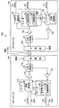
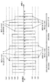
図9〜図11は、本実施形態において、第1の情報処理モジュール102と第2の情報処理モジュール104と間で送受信される信号パターンの一例を示す説明図である。各図では、基準電圧である5.0Vを中心とし、クロック信号のエッジ間隔を時間Tの1単位として、エッジごとの信号の振幅値の移り変わりが時間軸に沿って実線で示されている。このうち、T=1、3、5…のエッジはクロック信号の立ち上がりエッジ、T=2、4、6…のエッジはクロック信号の立ち下がりエッジである。
[3-2. Example of signal pattern]
9 to 11 are explanatory diagrams illustrating an example of signal patterns transmitted and received between the first information processing module 102 and the second information processing module 104 in the present embodiment. In each figure, the transition of the amplitude value of the signal for each edge is indicated by a solid line along the time axis, with the reference voltage of 5.0V as the center and the edge interval of the clock signal as one unit of time T. Of these, the edges T = 1, 3, 5,... Are the rising edges of the clock signal, and the edges T = 2, 4, 6,... Are the falling edges of the clock signal.
まず、図9を参照すると、T=1〜4の期間には、クロック信号のみが第1の情報処理モジュール102から第2の情報処理モジュール104へ供給されている。クロック信号の立ち上がりエッジの振幅値は6.0V、立ち下がりエッジの振幅値は4.0Vである。 First, referring to FIG. 9, only the clock signal is supplied from the first information processing module 102 to the second information processing module 104 during a period of T = 1 to 4. The amplitude value of the rising edge of the clock signal is 6.0V, and the amplitude value of the falling edge is 4.0V.
次に、T=5、7、9のクロック信号の立ち上がりエッジに、第1の情報処理モジュール102によりデータ信号(TX DATA1)が重畳されている。ここでの信号値は、“1”、“0”、“1”である。また、信号値“1”の振幅値は6.2V、信号値“0”の振幅値は5.8Vである。これに対し、T=6、8、10のクロック信号の立ち下がりエッジに、第2の情報処理モジュール104により送達確認信号(ACK)が重畳されている。データ信号の信号値“1”に対する送達確認信号の振幅値は3.8V、データ信号の信号値“0”に対する送達確認信号の振幅値は4.2Vである。 Next, the data signal (TX DATA1) is superimposed by the first information processing module 102 on the rising edge of the clock signal at T = 5, 7, and 9. The signal values here are “1”, “0”, and “1”. The amplitude value of the signal value “1” is 6.2V, and the amplitude value of the signal value “0” is 5.8V. On the other hand, the delivery confirmation signal (ACK) is superimposed by the second information processing module 104 on the falling edges of the clock signals of T = 6, 8, and 10. The amplitude value of the delivery confirmation signal with respect to the signal value “1” of the data signal is 3.8 V, and the amplitude value of the delivery confirmation signal with respect to the signal value “0” of the data signal is 4.2 V.
次に、T=11〜14の期間には、再びクロック信号のみが第1の情報処理モジュール102から第2の情報処理モジュール104へ供給されている。 Next, only the clock signal is supplied from the first information processing module 102 to the second information processing module 104 again during a period of T = 11 to 14.
次に、T=15、17、19のクロック信号の立ち上がりエッジに、第2の情報処理モジュール104によりデータ信号(TX DATA2)が重畳されている。ここでの信号値は、“0”、“1”、“0”である。また、信号値“1”の振幅値は6.2V、信号値“0”の振幅値は5.8Vである。これに対し、T=16、18、20のクロック信号の立ち下がりエッジに、第1の情報処理モジュール102により送達確認信号(ACK)が重畳されている。データ信号の信号値“1”に対する送達確認信号の振幅値は3.8V、データ信号の信号値“0”に対する送達確認信号の振幅値は4.2Vである。 Next, the data signal (TX DATA2) is superimposed by the second information processing module 104 on the rising edge of the clock signal at T = 15, 17, and 19. The signal values here are “0”, “1”, and “0”. The amplitude value of the signal value “1” is 6.2V, and the amplitude value of the signal value “0” is 5.8V. On the other hand, the delivery confirmation signal (ACK) is superimposed by the first information processing module 102 on the falling edges of the clock signals of T = 16, 18, and 20. The amplitude value of the delivery confirmation signal with respect to the signal value “1” of the data signal is 3.8 V, and the amplitude value of the delivery confirmation signal with respect to the signal value “0” of the data signal is 4.2 V.
このような振幅値の制御により、信号電圧の直流成分の変動が打ち消されるため、第1の情報処理モジュール102から第2の情報処理モジュール104へ電源を供給する電源線を信号線として使用することが容易となる。また、不正ユーザが信号線の電圧を監視したとしても、その電圧がどちらのモジュールからの信号の送信によるものかを知ることができないため、信号の内容を解釈することは困難となる Since the fluctuation of the DC component of the signal voltage is canceled by such control of the amplitude value, the power supply line that supplies power from the first information processing module 102 to the second information processing module 104 is used as the signal line. Becomes easy. Even if an unauthorized user monitors the voltage of a signal line, it is difficult to interpret the content of the signal because it cannot know which module is transmitting the signal.
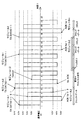
次に、図10を参照すると、信号の衝突が発生した際の信号パターンの一例が示されている。 Next, referring to FIG. 10, an example of a signal pattern when a signal collision occurs is shown.
まず、T=1、3のクロック信号の立ち上がりエッジに、第1の情報処理モジュール102によりデータ信号(TX DATA1)が重畳されている。これに対し、T=2、4のクロック信号の立ち下がりエッジに、第2の情報処理モジュール104により送達確認信号(ACK)が重畳されている。その後、T=5の立ち上がりエッジに、第1の情報処理モジュール102からのデータ信号と第2の情報処理モジュール104からのデータ信号が同時に重畳されている。即ち、T=5において信号の衝突が発生し、信号線の電圧は6.4Vとなっている。そのため、T=6の立ち下がりエッジでは、どちらのモジュールからも送達確認信号が送信されず、信号線の電圧はクロック信号の立ち下がりエッジの4.0Vのままとなる。そうすると、信号の衝突を検知した第1の情報処理モジュール102及び第2の情報処理モジュール104により、T=7の立ち上がりエッジにキャンセル信号が重畳されている。この場合のキャンセル信号が重畳されたクロック信号の振幅値は5.6Vである。 First, the data signal (TX DATA1) is superimposed on the rising edge of the clock signal of T = 1, 3 by the first information processing module 102. On the other hand, a delivery confirmation signal (ACK) is superimposed by the second information processing module 104 on the falling edge of the clock signal of T = 2, 4. Thereafter, the data signal from the first information processing module 102 and the data signal from the second information processing module 104 are simultaneously superimposed on the rising edge of T = 5. That is, a signal collision occurs at T = 5, and the voltage of the signal line is 6.4V. Therefore, at the falling edge of T = 6, no acknowledgment signal is transmitted from either module, and the voltage of the signal line remains 4.0 V, which is the falling edge of the clock signal. Then, the cancel signal is superimposed on the rising edge of T = 7 by the first information processing module 102 and the second information processing module 104 that have detected the signal collision. In this case, the amplitude value of the clock signal on which the cancel signal is superimposed is 5.6V.
その後、第1の情報処理モジュール102及び第2の情報処理モジュール104は、それぞれ再送する信号の衝突を回避するために、ランダムバックオフを行う。例えば、図10の例では、第1の情報処理モジュール102はT=9〜12の間、信号の送信を待機している。一方、第2の情報処理モジュール104はT=9〜16の間、信号の送信を待機している。 Thereafter, the first information processing module 102 and the second information processing module 104 perform random backoff in order to avoid collision of signals to be retransmitted. For example, in the example of FIG. 10, the first information processing module 102 waits for signal transmission during T = 9-12. On the other hand, the second information processing module 104 stands by for signal transmission during T = 9-16.
そして、先にバックオフ期間が終了した第1の情報処理モジュール102により、T=13のクロック信号の立ち上がりエッジに、データ信号が重畳されている。これに対し、T=14のクロック信号の立ち下がりエッジに、第2の情報処理モジュール104により送達確認信号が重畳されている。また、遅れてバックオフ期間が終了した第2の情報処理モジュール104により、T=17のクロック信号の立ち上がりエッジに、データ信号が重畳されている。これに対し、T=18のクロック信号の立ち下がりエッジに、第1の情報処理モジュール102より送達確認信号が重畳されている。 Then, the data signal is superimposed on the rising edge of the clock signal at T = 13 by the first information processing module 102 that has finished the back-off period. On the other hand, the delivery confirmation signal is superimposed by the second information processing module 104 on the falling edge of the clock signal of T = 14. Further, the data signal is superimposed on the rising edge of the clock signal of T = 17 by the second information processing module 104 whose back-off period has ended with a delay. On the other hand, the delivery confirmation signal is superimposed from the first information processing module 102 on the falling edge of the clock signal of T = 18.
次に、図11を参照すると、ダミーデータ信号送信処理に関する信号パターンの一例が示されている。なお、ここでは、第1の情報処理モジュール102の送信制御部128のみがダミーデータ送信機能を実行する場合を例にとり説明する。
Next, referring to FIG. 11, an example of a signal pattern related to dummy data signal transmission processing is shown. Here, a case where only the
まず、T=1、3のクロック信号の立ち上がりエッジに、第1の情報処理モジュール102によりデータ信号(TX DATA1)が重畳されている。ここでの信号値は、“1”、“1”である。これに対し、T=2、4のクロック信号の立ち下がりエッジに、第2の情報処理モジュール104により送達確認信号(ACK)が重畳されている。 First, the data signal (TX DATA1) is superimposed on the rising edge of the clock signal of T = 1, 3 by the first information processing module 102. The signal values here are “1” and “1”. On the other hand, a delivery confirmation signal (ACK) is superimposed by the second information processing module 104 on the falling edge of the clock signal of T = 2, 4.
次に、T=5〜8の期間には、クロック信号のみが第1の情報処理モジュール102から第2の情報処理モジュール104へ供給されている。 Next, only the clock signal is supplied from the first information processing module 102 to the second information processing module 104 during a period of T = 5 to 8.
次に、T=9のクロック信号の立ち上がりエッジに、第2の情報処理モジュール104によりデータ信号(TX DATA2)が重畳されている。ここでの信号値は、“1”である。これに対し、T=10のクロック信号の立ち下がりエッジに、第1の情報処理モジュール102により送達確認信号(ACK)が重畳されている。さらに、T=11のクロック信号の立ち上がりエッジに、第1の情報処理モジュール102によりダミーデータ信号が重畳されている。ここでは、ダミーデータ信号として、直前に受信されたデータ信号と同一のビットパターンを有する信号(即ち、信号値“1”のエコーバック)が使用されている。これに対し、T=12のクロック信号の立ち下がりエッジに、第2の情報処理モジュール104により送達確認信号(ACK)が重畳されている。このとき、第2の情報処理モジュール104は、受信した信号のビットパターンを直前に送信した信号のビットパターンと比較することにより、受信した信号がダミーデータ信号であることを識別することができる。 Next, the data signal (TX DATA2) is superimposed by the second information processing module 104 on the rising edge of the clock signal at T = 9. The signal value here is “1”. On the other hand, a delivery confirmation signal (ACK) is superimposed by the first information processing module 102 on the falling edge of the clock signal of T = 10. Further, a dummy data signal is superimposed by the first information processing module 102 on the rising edge of the clock signal at T = 11. Here, as the dummy data signal, a signal having the same bit pattern as the data signal received immediately before (that is, an echo back of the signal value “1”) is used. On the other hand, the delivery confirmation signal (ACK) is superimposed by the second information processing module 104 on the falling edge of the clock signal of T = 12. At this time, the second information processing module 104 can identify that the received signal is a dummy data signal by comparing the bit pattern of the received signal with the bit pattern of the signal transmitted immediately before.
その後、T=13〜16の期間には、再びクロック信号のみが第1の情報処理モジュール102から第2の情報処理モジュール104へ供給されている。 Thereafter, only the clock signal is supplied from the first information processing module 102 to the second information processing module 104 again during a period of T = 13 to 16.
このような信号パターンにおいて、例えば図6に示した本実施形態に係る振幅変調の振幅値の定義を知っている不正ユーザが信号線の電圧を読み取ったとする。その場合、読み取られる信号パターンは、“1”、“1”、“1”、“1”となる。しかし、かかる信号パターンの各信号値が、いずれのモジュールから送信されたのか、又はデータ信号なのかダミーデータ信号なのかを知ることは、不正ユーザにとって主に次の2つの理由により困難である。まず、第1の理由として、ダミーデータ信号も通常のデータ信号も信号線の電圧値は同一である。そのため、例えば図11では、T=1〜4において送受信された2ビットのデータ信号と、T=9〜12において送受信された1ビットのデータ信号及び1ビットのダミーデータ信号との間で、外見上の電圧値に相違はない。第2の理由として、例えば図11では、T=5〜8においてクロック信号のみが送信されているが、これは非衝突時のバックオフによるものである可能性がある。即ち、例えば、第1の情報処理モジュール102が信号値“1”、“1”、“1”、“1”の信号パターンを有するデータ信号を送信しようとした場合でも、図11と同等の信号パターンが観測される可能性がある。それにより、不正ユーザは信号の区切り自体を正確に知得することができず、観測したデータを信号の区切りをヒントにして解析することが困難となる。 In such a signal pattern, it is assumed that an unauthorized user who knows the definition of the amplitude value of the amplitude modulation according to the present embodiment shown in FIG. 6 reads the voltage of the signal line. In this case, the read signal pattern is “1”, “1”, “1”, “1”. However, it is difficult for an unauthorized user to know from which module each signal value of the signal pattern is transmitted, a data signal, or a dummy data signal mainly for the following two reasons. First, as a first reason, the voltage value of the signal line is the same for both the dummy data signal and the normal data signal. Therefore, for example, in FIG. 11, there is an appearance between a 2-bit data signal transmitted / received at T = 1 to 4 and a 1-bit data signal and 1-bit dummy data signal transmitted / received at T = 9-12. There is no difference in the voltage values above. As a second reason, for example, in FIG. 11, only the clock signal is transmitted at T = 5 to 8, but this may be due to back-off at the time of non-collision. That is, for example, even when the first information processing module 102 attempts to transmit a data signal having a signal pattern of signal values “1”, “1”, “1”, “1”, the same signal as in FIG. Patterns may be observed. As a result, an unauthorized user cannot accurately know the signal separation itself, and it becomes difficult to analyze the observed data using the signal separation as a hint.
なお、図9〜図11では、説明の明瞭さの観点から、ビット数の少ない単純な信号パターンを例にとって説明を行った。しかしながら、本実施形態に係る情報処理装置100において送受信されるデータ信号、確認応答信号、キャンセル信号、又はダミーデータ信号などの信号のビット数及び信号パターンは、かかる例に限定されず、どのような値であってもよい。
In FIGS. 9 to 11, for the sake of clarity of explanation, a simple signal pattern with a small number of bits has been described as an example. However, the number of bits and the signal pattern of a signal such as a data signal, an acknowledgment signal, a cancel signal, or a dummy data signal transmitted and received in the
<4.まとめ>
ここまで、図1〜図11を用いて、本発明の一実施形態に係る情報処理装置100について説明した。
<4. Summary>
So far, the
本実施形態に係る情報処理装置100よれば、2つの情報処理モジュールの間で、クロック信号の立ち上がりエッジと立ち下がりエッジにそれぞれデータ信号と送達確認信号を重畳させることで、例えば時分割伝送方式を採用することなく、双方向通信が実現される。それにより、例えばセキュリティの低下を避けるために時分割伝送方式のタイムスロットの定義などを秘匿する必要性が排除される。
According to the
また、送信すべきデータ信号が存在しない任意の時点で、いずれかの情報処理モジュールによりダミーデータ信号がクロック信号の立ち上がりエッジに重畳される。それにより、データの送受信が散発的にしか生じない場合であっても、通信データの内容を不正ユーザが解釈することが困難となる。 In addition, at any time when there is no data signal to be transmitted, the dummy data signal is superimposed on the rising edge of the clock signal by any information processing module. This makes it difficult for an unauthorized user to interpret the contents of communication data even when data transmission / reception occurs only sporadically.
また、データ信号の衝突を検知していない場合にも、連続するデータ信号が所定の時間間隔を空けてクロック信号の立ち上がりエッジに重畳され得る。それにより、不正ユーザにとっては、送信されるデータのまとまりを正確に認識して一連のデータ信号を正しく組み立てることが困難となる。 Even when no collision of data signals is detected, continuous data signals can be superimposed on the rising edge of the clock signal with a predetermined time interval. Thus, it becomes difficult for an unauthorized user to correctly recognize a group of data to be transmitted and correctly assemble a series of data signals.
さらに、情報処理装置100において、第1の情報処理モジュール102から第2の情報処理モジュール104へ、クロック信号と共通の信号線を用いて電力が供給される。かかる電力の直流成分は、本実施形態に一例として示した振幅値の定義により、一定の値に維持される。また、電力線と信号線が共通化されることから、例えば情報処理モジュール間の信号線に流れる電流を検知して信号の内容を知得しようとするセキュリティ上の攻撃も防ぐことができる。
Further, in the
こうした情報処理モジュール間の通信セキュリティの向上により、情報処理装置100において、装置内に暗号化及び復号のための追加的な回路を持つことを省略することができる。その代わりに、例えば、情報処理装置100に追加的な暗号化手段を設けることで、情報処理モジュール間の通信セキュリティをさらに強固にすることができる。
Due to such improved communication security between information processing modules, the
なお、上記以外の本明細書において説明した情報処理装置100の各特徴も、情報処理装置100における情報処理モジュール間の通信セキュリティの向上に寄与していることは言うまでもない。
Needless to say, the features of the
ここで、本明細書において説明した情報処理装置100による一連の処理は、ハードウェアで実現されてもよく、又はソフトウェアで実現されてもよい。一連の処理又はその一部をソフトウェアで実行させる場合には、例えば、ソフトウェアを構成するプログラムが予めROMに格納され、実行時にRAMに読み込まれてCPUにより実行される。
Here, a series of processing by the
以上、添付図面を参照しながら本発明の好適な実施形態について説明したが、本発明は係る例に限定されないことは言うまでもない。当業者であれば、特許請求の範囲に記載された範疇内において、各種の変更例又は修正例に想到し得ることは明らかであり、それらについても当然に本発明の技術的範囲に属するものと了解される。 As mentioned above, although preferred embodiment of this invention was described referring an accompanying drawing, it cannot be overemphasized that this invention is not limited to the example which concerns. It will be apparent to those skilled in the art that various changes and modifications can be made within the scope of the claims, and these are naturally within the technical scope of the present invention. Understood.
例えば、情報処理装置100において、3つ以上の情報処理モジュールの間で通信を行う場合にも、本発明は適用可能である。
For example, the present invention can also be applied when the
また、例えば、図8を用いて説明した通信処理を、必ずしもフローチャートに記載された順序に沿って実行しなくてもよい。各処理ステップは、並列的あるいは個別に独立して実行される処理を含んでもよい。 Further, for example, the communication process described with reference to FIG. 8 does not necessarily have to be executed in the order described in the flowchart. Each processing step may include processing executed in parallel or individually independently.
100 情報処理装置
102 第1の情報処理モジュール
103 接続部
104 第2の情報処理モジュール
106 シリアライザ/デシリアライザ(M)
108 シリアライザ/デシリアライザ(D)
112 エンコーダ
114 ドライバ
116、134 合成分配器
118 重畳部
120、136 レシーバ
122、140 デコーダ
124、148 送達確認部
126、150 衝突検知部
128、152 送信制御部
132 分離部
138 クロック検出部
142 バンドパスフィルタ(BPF)
DESCRIPTION OF
108 Serializer / Deserializer (D)
112
Claims (9)
前記第1の情報処理モジュールは;
クロック信号を前記信号線に送出し、及びデータ信号を当該クロック信号の立ち上がりエッジに重畳し、
並びに、前記信号線を介して受信したデータ信号に対する送達確認信号を前記クロック信号の立ち下がりエッジに重畳し、
前記第2の情報処理モジュールは;
前記第1の情報処理モジュールにより前記信号線に送出される前記クロック信号の立ち上がりエッジにデータ信号を重畳し、
及び、前記信号線を介して受信したデータ信号に対する送達確認信号を前記クロック信号の立ち下がりエッジに重畳する、
情報処理装置。 A first information processing module and a second information processing module connected to each other by a signal line include:
The first information processing module;
Send a clock signal to the signal line, and superimpose a data signal on the rising edge of the clock signal;
In addition, a delivery confirmation signal for the data signal received via the signal line is superimposed on the falling edge of the clock signal,
The second information processing module;
Superimposing a data signal on the rising edge of the clock signal sent to the signal line by the first information processing module;
And superimposing a delivery confirmation signal for the data signal received via the signal line on the falling edge of the clock signal,
Information processing device.
前記第1の情報処理モジュールにより、クロック信号の立ち上がりエッジにデータ信号を重畳するステップと;
前記第1の情報処理モジュールにより、前記クロック信号を前記信号線に送出するステップと;
前記第2の情報処理モジュールにより、前記クロック信号に重畳された前記データ信号を受信するステップと;
前記第2の情報処理モジュールにより、受信したデータ信号に対する送達確認信号を前記クロック信号の立ち下がりエッジに重畳するステップと;
前記第1の情報処理モジュールにより、当該送達確認信号を受信するステップと;
を含むデータ伝送方法。
In an information processing apparatus comprising a first information processing module and a second information processing module connected to each other via a signal line:
Superimposing a data signal on a rising edge of a clock signal by the first information processing module;
Sending the clock signal to the signal line by the first information processing module;
Receiving the data signal superimposed on the clock signal by the second information processing module;
Superimposing a delivery confirmation signal for the received data signal on the falling edge of the clock signal by the second information processing module;
Receiving the delivery confirmation signal by the first information processing module;
A data transmission method including:
Priority Applications (1)
| Application Number | Priority Date | Filing Date | Title |
|---|---|---|---|
| JP2008315616A JP2010141569A (en) | 2008-12-11 | 2008-12-11 | Information processor and data transmission method |
Applications Claiming Priority (1)
| Application Number | Priority Date | Filing Date | Title |
|---|---|---|---|
| JP2008315616A JP2010141569A (en) | 2008-12-11 | 2008-12-11 | Information processor and data transmission method |
Publications (1)
| Publication Number | Publication Date |
|---|---|
| JP2010141569A true JP2010141569A (en) | 2010-06-24 |
Family
ID=42351308
Family Applications (1)
| Application Number | Title | Priority Date | Filing Date |
|---|---|---|---|
| JP2008315616A Withdrawn JP2010141569A (en) | 2008-12-11 | 2008-12-11 | Information processor and data transmission method |
Country Status (1)
| Country | Link |
|---|---|
| JP (1) | JP2010141569A (en) |
Cited By (1)
| Publication number | Priority date | Publication date | Assignee | Title |
|---|---|---|---|---|
| JP2018170796A (en) * | 2018-07-26 | 2018-11-01 | 株式会社三菱Ufj銀行 | Server and terminal |
-
2008
- 2008-12-11 JP JP2008315616A patent/JP2010141569A/en not_active Withdrawn
Cited By (1)
| Publication number | Priority date | Publication date | Assignee | Title |
|---|---|---|---|---|
| JP2018170796A (en) * | 2018-07-26 | 2018-11-01 | 株式会社三菱Ufj銀行 | Server and terminal |
Similar Documents
| Publication | Publication Date | Title |
|---|---|---|
| US7558326B1 (en) | Method and apparatus for sending auxiliary data on a TMDS-like link | |
| US7295578B1 (en) | Method and apparatus for synchronizing auxiliary data and video data transmitted over a TMDS-like link | |
| US11057213B2 (en) | Authentication system for electronic control unit on a bus | |
| KR101669946B1 (en) | Appratus and method for identification of ecu using voltage signal | |
| US8874895B2 (en) | Data transmitting apparatus, data receiving apparatus, data transmitting method, and data receiving method | |
| US20120221859A1 (en) | Strong authentication token with acoustic data input | |
| EP3089498B1 (en) | Signal modulation for secure communication | |
| US8077645B2 (en) | Wireless communication terminal, semiconductor device, data communication method, and wireless communication system | |
| US20210306177A1 (en) | Adaptable and Secure Can Bus | |
| US20140205095A1 (en) | Authentication system and authentication code convertor | |
| US8907766B2 (en) | Method and system for secure communication | |
| CA2405022A1 (en) | Method and apparatus for secure transmission of data | |
| CN117397187A (en) | Transmitting device, receiving device, parameter adjustment method, SerDes circuit and electronic equipment | |
| US20060041576A1 (en) | Data processsing deviceand data reception processing device | |
| JP2010141569A (en) | Information processor and data transmission method | |
| US7266694B2 (en) | Network relay device, communication device and network relay method | |
| CN115798086B (en) | Anti-interference method and device for intelligent door lock, equipment and storage medium | |
| JP2020167570A (en) | Monitoring device | |
| JP2004208260A (en) | Radio communication terminal device | |
| KR102727466B1 (en) | Wireless Communication Interface with Function for Generating Physical Random Numbers | |
| US20090182926A1 (en) | Electronic apparatus and information transfer method | |
| JP2008085576A (en) | Data communication system, data transmission device, data reception device, and data communication method | |
| JPH0446495B2 (en) | ||
| JP2009060341A (en) | COMMUNICATION SYSTEM, RECEPTION DEVICE, TRANSMISSION DEVICE, AND COMMUNICATION METHOD | |
| JP2000236527A (en) | Descrambling system in catv system |
Legal Events
| Date | Code | Title | Description |
|---|---|---|---|
| A300 | Application deemed to be withdrawn because no request for examination was validly filed |
Free format text: JAPANESE INTERMEDIATE CODE: A300 Effective date: 20120306 |