JP2010141056A - Ceramic substrate and method of manufacturing the same - Google Patents
Ceramic substrate and method of manufacturing the same Download PDFInfo
- Publication number
- JP2010141056A JP2010141056A JP2008315001A JP2008315001A JP2010141056A JP 2010141056 A JP2010141056 A JP 2010141056A JP 2008315001 A JP2008315001 A JP 2008315001A JP 2008315001 A JP2008315001 A JP 2008315001A JP 2010141056 A JP2010141056 A JP 2010141056A
- Authority
- JP
- Japan
- Prior art keywords
- base material
- substrate
- thin film
- film layer
- ceramic
- Prior art date
- Legal status (The legal status is an assumption and is not a legal conclusion. Google has not performed a legal analysis and makes no representation as to the accuracy of the status listed.)
- Granted
Links
Images

Classifications
-
- H—ELECTRICITY
- H10—SEMICONDUCTOR DEVICES; ELECTRIC SOLID-STATE DEVICES NOT OTHERWISE PROVIDED FOR
- H10W—GENERIC PACKAGES, INTERCONNECTIONS, CONNECTORS OR OTHER CONSTRUCTIONAL DETAILS OF DEVICES COVERED BY CLASS H10
- H10W90/00—Package configurations
- H10W90/701—Package configurations characterised by the relative positions of pads or connectors relative to package parts
- H10W90/731—Package configurations characterised by the relative positions of pads or connectors relative to package parts of die-attach connectors
- H10W90/734—Package configurations characterised by the relative positions of pads or connectors relative to package parts of die-attach connectors between a chip and a stacked insulating package substrate, interposer or RDL
Landscapes
- Ceramic Products (AREA)
- Production Of Multi-Layered Print Wiring Board (AREA)
Abstract
【課題】表面の傷の検出を容易にしたセラミックス基板及びその製造方法を提供する。
【解決手段】セラミックスを焼結してなる母材基板11の表面に、該母材基板11と同質のセラミックスで母材基板11のセラミックス粒子よりも小さい微細粒子を焼結してなる傷検出用薄膜層12を、傷の許容限界深さよりも小さい膜厚で形成してなり、その微細粒子は、母材基板11のセラミックス粒子の平均粒径が10〜100μmであるのに対して、平均粒径が0.5〜3μmである。
【選択図】 図3A ceramic substrate and a method for manufacturing the same are provided.
A method for detecting flaws in which fine particles smaller than the ceramic particles of a base material substrate 11 are sintered on the surface of the base material substrate 11 formed by sintering ceramics. The thin film layer 12 is formed with a film thickness smaller than the permissible limit depth of scratches, and the fine particles have an average particle size of 10 to 100 μm of ceramic particles of the base material substrate 11. The diameter is 0.5-3 μm.
[Selection] Figure 3
Description
本発明は、パワーモジュール用基板等に用いられるセラミックス基板に係り、表面の傷の検出が容易なセラミックス基板及びその製造方法に関する。 The present invention relates to a ceramic substrate used for a power module substrate and the like, and more particularly to a ceramic substrate that can easily detect surface scratches and a method for manufacturing the same.
一般に、半導体素子の中でも電力供給のためのパワーモジュールは発熱量が比較的高いため、このパワーモジュール用基板としては、AlN、Al2O3、Si3N4、SiC等からなるセラミックス基板が用いられており、このセラミックス基板の上にアルミニウムの回路層がろう付けされ、その上に電子部品(半導体チップ等のパワー素子)が搭載されてパワーモジュールとされるようになっている。また、回路層とは反対側の面が放熱のために冷却器に取り付けられるが、近年では、構造簡略化等の要請に伴い、特許文献1に記載されるように、緩衝層や放熱用金属板を使わずにセラミックス基板を冷却器に直接接触させることが検討されており、パワーモジュールとしては過酷な環境(熱サイクル)への適用が要求されてきている。
その場合、セラミックス基板は、通常のハンドリングで表面にわずかなすり傷が発生し易く、熱サイクル環境の厳しい条件下で使用されると、その傷が起点となって割れにつながるおそれがある。このため、回路層を積層する前に、セラミックス基板表面の傷の有無を検査している。
In this case, the ceramic substrate is likely to be slightly scratched on the surface by normal handling, and when used under severe conditions in a thermal cycle environment, the scratch may start and lead to cracking. For this reason, before laminating circuit layers, the presence or absence of scratches on the ceramic substrate surface is inspected.
しかしながら、セラミックス基板の表面は微細な凹凸面であるため、微細な傷の場合は、セラミックス基板の表面の凹凸に隠れて検出することが困難であった。特に、カメラで撮影した画像をもとに自動検出することが不可能で、人間の目に頼らざるを得ず、作業効率が極めて悪いという問題があった。
本発明は、このような事情に鑑みてなされたものであって、表面の傷の検出を容易にしたセラミックス基板及びその製造方法を提供することを目的とする。
However, since the surface of the ceramic substrate is a fine concavo-convex surface, it is difficult to detect a fine flaw hidden behind the concavo-convex surface of the ceramic substrate. In particular, automatic detection based on images taken by a camera is impossible, and human eyes must be relied upon, and work efficiency is extremely poor.
This invention is made | formed in view of such a situation, Comprising: It aims at providing the ceramic substrate which made the detection of the flaw of a surface easy, and its manufacturing method.
本発明に係るセラミックス基板は、セラミックスを焼結してなる母材基板の表面に、該母材基板と同質のセラミックスで母材基板の粒子よりも小さい微細粒子を焼結してなる傷検出用薄膜層を形成したことを特徴とする。 The ceramic substrate according to the present invention is for flaw detection in which fine particles smaller than the particles of the base material substrate are sintered on the surface of the base material substrate obtained by sintering the ceramics with the same quality ceramic as the base material substrate. A thin film layer is formed.
このセラミックス基板では、母材基板の表面に形成されている傷検出用薄膜層は、母材基板のセラミックスの粒子よりも小さい微細粒子によって形成されていることから、傷検出用薄膜層の表面は母材基板の表面よりも平滑面に形成される。したがって、傷が傷検出用薄膜層を分断して母材基板まで達する場合には、平滑で微細な粒子からなる傷検出用薄膜層の傷口の中に、それより粗い粒子からなる母材基板のセラミックスが露出することになり、これらの粒子の大きさの差に基づくコントラストにより、傷の発見が容易になり、カメラでの撮影画像からの自動検出が可能になる。 In this ceramic substrate, the scratch detection thin film layer formed on the surface of the base material substrate is formed by fine particles smaller than the ceramic particles of the base material substrate. It is formed on a smoother surface than the surface of the base material substrate. Therefore, when the scratch divides the thin film layer for detecting scratches and reaches the base material substrate, the base material substrate made of coarser particles is placed in the wound of the thin film layer for scratch detection made of smooth and fine particles. Ceramics will be exposed, and the contrast based on the difference in the size of these particles facilitates the detection of scratches and enables automatic detection from images taken with a camera.
本発明に係るセラミックス基板において、その仕様で傷の深さに対して許容限界が定められている場合は、前記傷検出用薄膜層の膜厚は、傷の許容限界深さよりも小さいものとされる。
傷の深さが許容限界深さよりも大きくなると、傷検出用薄膜層を分断して母材基板にまで傷が達することになり、傷検出用薄膜層の傷口の中に母材基板のセラミックスが露出し、傷の検出が容易になる。傷の深さが小さくて傷検出用薄膜層の膜厚の範囲内で形成される場合は、傷口内にコントラストが生じないため発見が容易でないが、許容限界内であるので、製品としては支障ない。
In the ceramic substrate according to the present invention, if the specification defines an allowable limit for the depth of the flaw, the film thickness of the flaw detection thin film layer is assumed to be smaller than the allowable depth of the flaw. The
If the depth of the flaw becomes larger than the allowable limit depth, the flaw detection thin film layer is divided and the flaw reaches the base material substrate, and the ceramic of the base material substrate is placed in the flaw of the flaw detection thin film layer. Exposed and easy to detect scratches. If the depth of the scratch is small and it is formed within the range of the thickness of the thin film layer for scratch detection, it is not easy to find because there is no contrast in the wound, but it is within acceptable limits, so it is a problem as a product. Absent.
本発明に係るセラミックス基板において、前記母材基板のセラミックス粒子は、平均粒径が10〜100μmであり、傷検出用薄膜層の微細粒子は、平均粒径が0.5〜3μmであるとよい。
母材基板と傷検出用薄膜層との粒子の粒径がこのような組み合わせであると、母材基板と傷検出用薄膜層との粒径差が大きく、傷によるコントラストが際立つことから、容易に傷を検出することができる。
In the ceramic substrate according to the present invention, the ceramic particles of the base material substrate may have an average particle size of 10 to 100 μm, and the fine particles of the scratch detection thin film layer may have an average particle size of 0.5 to 3 μm. .
If the particle size of the base material substrate and the scratch detection thin film layer is such a combination, the difference in particle size between the base substrate and the scratch detection thin film layer is large and the contrast due to scratches stands out. Scratches can be detected.
また、本発明に係るセラミックス基板の製造方法は、セラミックス粒子をシート状に成形して焼結することにより前記母材基板を製作した後、該母材基板の表面を研磨することにより平坦化し、その平坦面の上に前記傷検出用薄膜層を形成することを特徴とする。
母材基板を製作すると、そのセラミックス粒子の大きさに起因して表面が微細な凹凸面に形成される。その上にそのまま傷検出用薄膜層を形成すると、母材基板の凹凸面が傷検出用薄膜層の表面に残ってしまうので、これを平坦化した後に傷検出用薄膜層を形成する。これにより、傷検出用薄膜層の表面が平坦になり、傷の検出が容易になる。
In addition, the method for manufacturing a ceramic substrate according to the present invention, after producing the base material substrate by molding and sintering ceramic particles into a sheet, and then flattening by polishing the surface of the base material substrate, The flaw detection thin film layer is formed on the flat surface.
When the base material substrate is manufactured, the surface is formed into a fine uneven surface due to the size of the ceramic particles. If the scratch detection thin film layer is formed as it is, the uneven surface of the base material substrate remains on the surface of the scratch detection thin film layer, and the scratch detection thin film layer is formed after planarizing the surface. As a result, the surface of the flaw detection thin film layer becomes flat, and flaw detection becomes easy.
この場合、前記平坦面を中心線平均粗さRaで0.3〜0.4μmの表面粗さにするとよい。
傷検出用薄膜層の微細粒子としては平均粒径が0.5〜3μmであるものが適切であり、その傷検出用薄膜層の下地となる母材基板の表面の表面粗さを中心線平均粗さRaで0.3〜0.4μmにすると、傷検出用薄膜層の微細粒子としての平滑性を有効に発揮させることができ、傷の検出を容易にすることができる。
また、傷検出用薄膜層の表面粗さは中心線平均粗さRaで0.1〜0.2μmとするとよい。
In this case, the flat surface may have a surface roughness of 0.3 to 0.4 μm in terms of centerline average roughness Ra.
As the fine particles of the scratch detection thin film layer, those having an average particle size of 0.5 to 3 μm are suitable, and the surface roughness of the surface of the base material substrate that is the base of the scratch detection thin film layer is the center line average. When the roughness Ra is set to 0.3 to 0.4 μm, the smoothness as the fine particles of the flaw detection thin film layer can be effectively exhibited, and the flaw detection can be facilitated.
The surface roughness of the scratch detection thin film layer is preferably 0.1 to 0.2 μm in terms of the center line average roughness Ra.
本発明によれば、傷検出用薄膜層を分断して母材基板まで傷が達する場合には、平滑で微細な粒子からなる傷検出用薄膜層とそれより粗い粒子からなる母材基板との粒子の大きさの差に基づくコントラストによって傷を容易に検出することができ、カメラでの撮影画像からの自動検出が可能になる。したがって、傷検出作業を容易にするとともに、その検出精度を向上させることができる。このセラミックス基板により傷の品質保証をすることにより、基板としての信頼性を高めることができ、これをパワーモジュール用絶縁基板として用いる場合には、過酷な熱サイクル環境下で割れにつながるような傷を有しないものを提供することができる。 According to the present invention, when a scratch reaches the base material substrate by dividing the scratch detection thin film layer, the scratch detection thin film layer composed of smooth and fine particles and a base material substrate composed of coarser particles are provided. Scratches can be easily detected by contrast based on the difference in particle size, and automatic detection from an image captured by a camera becomes possible. Therefore, it is possible to facilitate the flaw detection work and improve the detection accuracy. By assuring the quality of scratches with this ceramic substrate, it is possible to improve the reliability of the substrate, and when this is used as an insulating substrate for power modules, scratches that can lead to cracks under severe thermal cycling Can be provided.
以下、本発明の一実施形態を図面を参照しながら説明する。
図1は、本発明に係るセラミックス基板をパワーモジュール用基板の絶縁基板として用いてなるパワーモジュールを示している。この図1に示されるパワーモジュール1は、セラミックス基板2を有するパワーモジュール用基板3と、該パワーモジュール用基板3の表面に搭載された半導体チップ等の電子部品4と、パワーモジュール用基板3の裏面に接合された冷却器5とから構成されている。
Hereinafter, an embodiment of the present invention will be described with reference to the drawings.
FIG. 1 shows a power module using a ceramic substrate according to the present invention as an insulating substrate of a power module substrate. A power module 1 shown in FIG. 1 includes a power module substrate 3 having a
パワーモジュール用基板3は、セラミックス基板2の表面側に電子部品4を搭載するための回路層用金属板6が積層され、セラミックス基板2の裏面側に冷却器5が取り付けられる構成である。
回路層用金属板6は、純アルミニウム若しくはアルミニウム合金からなる金属板により形成され、セラミックス基板2にろう付けにより積層され、その金属板6がエッチング処理されて所望のパターンの回路層を構成している。ろう材としては、Al−Si系、Al−Ge系、Al−Cu系、Al−Mg系またはAl−Mn系等が使用される。また、この回路層用金属板7は、その表面にはんだの濡れ性を向上させるために、ニッケルメッキ処理によってニッケルメッキ膜7が形成される。
The power module substrate 3 is configured such that a circuit
The circuit
そして、回路層用金属板6の上に、Sn−Ag−Cu系、Zn−Al系若しくはPb−Sn系等のはんだ材によって電子部品4が接合される。図中符号8がそのはんだ接合層を示す。なお、電子部品4と回路層用金属板6の端子部との間は、アルミニウムからなるボンディングワイヤ(図示略)により接続される。
一方、冷却器5は、アルミニウム合金の押し出し成形によって形成され、その長さ方向に沿って冷却水を流通させるための多数の流路9が形成されており、セラミックス基板2との間はろう付けによって接合される。
And the electronic component 4 is joined on the
On the other hand, the cooler 5 is formed by extrusion molding of an aluminum alloy, and is formed with a large number of
そして、このパワーモジュール用基板3に用いられるセラミックス基板2は、母材基板11の表面側に傷検出用薄膜層12が形成された構成である。母材基板11は、例えば窒化アルミニウム(AlN)により形成される。また、傷検出用薄膜層12は母材基板11と同じ窒化アルミニウム(AlN)により形成される。この場合、母材基板11を構成している窒化アルミニウムの粒子は、平均粒径が10〜100μmとされ、傷検出用薄膜層12を構成する窒化アルミニウムの粒子は、平均粒径が0.5〜3μmとされる(以後、母材基板11の粒子を粗粒子、傷検出用薄膜層12の粒子を微細粒子ということがある)。最大粒子径は、母材基板11で300μm、傷検出用薄膜層12で10μmとされる。また、傷検出用薄膜層12の膜厚は、セラミックス基板2に対する要求品質に応じて5〜10μmの範囲で設定される。
ここで平均粒径は、電子顕微鏡観察において測定方向を一定にして直径を測定した粒子径分布の小粒子径側からの積算値50体積%となる粒子径をいう。
The
Here, the average particle diameter refers to a particle diameter that becomes an integrated value of 50% by volume from the small particle diameter side of the particle diameter distribution measured with the measurement direction constant in electron microscope observation.
次に、このような構成のパワーモジュール1に使用されているセラミックス基板2の製造方法について説明する。
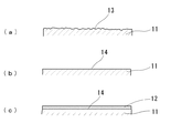
まず、母材基板11を形成する。この母材基板11を形成するには、窒化アルミニウム(AlN)の原料粉末に酸化イットリウム(Y2O3)等の焼結助剤及び有機バインダーを配合した後、ドクターブレード法又はプレス成形によりシート成形体を製作する。この窒化アルミニウムの平均粒径は10〜100μmとされる。そして、このシート成形体を空気中又は窒素雰囲気中で400〜460℃に加熱してバインダーを除去した後、窒素雰囲気等の非酸化性雰囲気中で常圧下において1900〜2000℃に加熱して焼結することにより母材基板11が形成される。この母材基板11は、図2(a)に示すように、その表面がセラミックスの粒子(粗粒子)の大きさに応じた凹凸面13に形成される。
次いで、この母材基板11の表面側をホーニング加工等により研磨する。ホーニング加工は、水に例えばアルミナ(Al2O3)粒子等の研磨材を分散させた状態で、高圧で基板表面に吹き付ける湿式ホーニング法、研磨材のみをエアーを用いて高圧で基板表面に吹き付ける乾式ホーニング法がある。このホーニング加工により、図2(b)に示すように、母材基板11の表面を中心線平均粗さRaで0.3〜0.4μmの表面粗さの平坦面14とする。
Next, a method for manufacturing the
First, the
Next, the surface side of the
次に、この母材基板11の平坦面14の上に、窒化アルミニウム(AlN)の原料粉末に酸化イットリウム(Y2O3)等の焼結助剤及び有機バインダーを配合した後、ドクターブレード法により重ね塗りすることにより、又はプレス成形によりシート状に成形したものを積層することにより、薄膜層を形成する。このときの窒化アルミニウムの平均粒径は0.5〜3μmとされる。そして、このシート成形体に積層された薄膜層を空気中又は窒素雰囲気中で400〜460℃に加熱してバインダーを除去した後、窒素雰囲気等の非酸化性雰囲気中で常圧下において1900〜2000℃に加熱して焼結することにより、図2(c)に示すように、母材基板11の上に微細粒子からなる傷検出用薄膜層12が形成される。この傷検出用薄膜層12の表面は中心線平均粗さRaで0.1〜0.2μmとする。
なお、母材基板11は焼結工程を2回経由することになるので、1回目は2回目より温度を低く設定しておくとよい。
Next, after blending a sintering aid such as yttrium oxide (Y 2 O 3 ) and an organic binder into the raw material powder of aluminum nitride (AlN) on the
In addition, since the base material board |
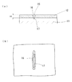
このようにして形成されたセラミックス基板2において、そのハンドリング中などに傷が発生した場合、図3(a)に示すように、その傷15が表面の傷検出用薄膜層12を分断して母材基板11にまで達する場合は、微細粒子により平滑な傷検出用薄膜層12の傷口を形成する微細粒子面16の中に、それより粗い粒子のために比較的凹凸が大きい母材基板11の粗粒子面17が露出することになり、これらの粒子の大きさの差に基づくコントラストにより、傷15の発見が容易になり、カメラでの撮影画像からの自動検出が可能になる。
In the
したがって、このセラミックス基板2においては、その傷検出用薄膜層12の膜厚Hよりも大きい傷が生じた場合には、傷検出用薄膜層12と母材基板11との粒子の大きさの差に基づくコントラストにより、傷を容易に検出することができる。これを逆に言えば、傷検出用薄膜層12の膜厚Hを、このセラミックス基板2に対する要求品質で規定される傷の許容限界よりも小さい寸法に設定しておくことにより、不良となる傷を確実に発見することができる。
また、このセラミックス基板2は、パワーモジュール用基板3としては、表面が傷検出用薄膜層12により平滑面に仕上げられているので、その上にろう付けされる回路層用金属板6のろう付け性が良く、これらの密着性が向上する。
このため、このセラミックス基板2を用いたパワーモジュール用基板3は、傷による不良品を確実に排除できるので、過酷な熱サイクル条件でも割れ等が生じにくく、また、回路層用金属板6の密着性も良く、基板としての信頼性を高めることができる。
Therefore, in the
Further, since the
For this reason, since the power module substrate 3 using the
以上、本発明の実施形態について図面を参照して詳述したが、具体的な構成はこの実施形態に限られるものではなく、本発明の要旨を逸脱しない範囲の設計変更等も含まれる。
例えば、母材基板を構成する材料としては、AlN(窒化アルミニウム)の他にも、Si3N4(窒化珪素)等の窒化物系セラミックス、若しくはAl2O3(アルミナ)等の酸化物系セラミックス等も適用可能である。傷検出用薄膜層は、母材基板の材料と同質の材料が使用される。
As mentioned above, although embodiment of this invention was explained in full detail with reference to drawings, the concrete structure is not restricted to this embodiment, The design change etc. of the range which does not deviate from the summary of this invention are included.
For example, as a material constituting the base material substrate, in addition to AlN (aluminum nitride), nitride ceramics such as Si 3 N 4 (silicon nitride), or oxides such as Al 2 O 3 (alumina) Ceramics and the like are also applicable. The flaw detection thin film layer is made of the same material as that of the base material substrate.
1 パワーモジュール
2 セラミックス基板
3 パワーモジュール用基板
4 電子部品
5 冷却器
6 回路層用金属板
7 ニッケルメッキ膜
8 はんだ接合層
9 流路
11 母材基板
12 傷検出用薄膜層
13 凹凸面
14 平坦面
15 傷
16 微細粒子面
17 粗粒子面
DESCRIPTION OF SYMBOLS 1
Claims (6)
セラミックス粒子をシート状に成形して焼結することにより前記母材基板を製作した後、該母材基板の表面を研磨することにより平坦化し、その平坦面の上に前記傷検出用薄膜層を形成することを特徴とするセラミックス基板の製造方法。 A method for producing a ceramic substrate according to any one of claims 1 to 3,
After forming the base material substrate by forming and sintering ceramic particles into a sheet shape, the surface of the base material substrate is flattened by polishing, and the scratch detecting thin film layer is formed on the flat surface. A method for manufacturing a ceramic substrate, comprising: forming a ceramic substrate.
Priority Applications (1)
| Application Number | Priority Date | Filing Date | Title |
|---|---|---|---|
| JP2008315001A JP5195379B2 (en) | 2008-12-10 | 2008-12-10 | Ceramic substrate and manufacturing method thereof |
Applications Claiming Priority (1)
| Application Number | Priority Date | Filing Date | Title |
|---|---|---|---|
| JP2008315001A JP5195379B2 (en) | 2008-12-10 | 2008-12-10 | Ceramic substrate and manufacturing method thereof |
Publications (2)
| Publication Number | Publication Date |
|---|---|
| JP2010141056A true JP2010141056A (en) | 2010-06-24 |
| JP5195379B2 JP5195379B2 (en) | 2013-05-08 |
Family
ID=42350946
Family Applications (1)
| Application Number | Title | Priority Date | Filing Date |
|---|---|---|---|
| JP2008315001A Expired - Fee Related JP5195379B2 (en) | 2008-12-10 | 2008-12-10 | Ceramic substrate and manufacturing method thereof |
Country Status (1)
| Country | Link |
|---|---|
| JP (1) | JP5195379B2 (en) |
Citations (2)
| Publication number | Priority date | Publication date | Assignee | Title |
|---|---|---|---|---|
| JPH04280694A (en) * | 1991-03-08 | 1992-10-06 | Ngk Insulators Ltd | Ceramic board and manufacture thereof |
| WO2005098942A1 (en) * | 2004-04-05 | 2005-10-20 | Mitsubishi Materials Corporation | Al/AlN JOINT MATERIAL, BASE PLATE FOR POWER MODULE, POWER MODULE AND PROCESS FOR PRODUCING Al/AlN JOINT MATERIAL |
-
2008
- 2008-12-10 JP JP2008315001A patent/JP5195379B2/en not_active Expired - Fee Related
Patent Citations (2)
| Publication number | Priority date | Publication date | Assignee | Title |
|---|---|---|---|---|
| JPH04280694A (en) * | 1991-03-08 | 1992-10-06 | Ngk Insulators Ltd | Ceramic board and manufacture thereof |
| WO2005098942A1 (en) * | 2004-04-05 | 2005-10-20 | Mitsubishi Materials Corporation | Al/AlN JOINT MATERIAL, BASE PLATE FOR POWER MODULE, POWER MODULE AND PROCESS FOR PRODUCING Al/AlN JOINT MATERIAL |
Also Published As
| Publication number | Publication date |
|---|---|
| JP5195379B2 (en) | 2013-05-08 |
Similar Documents
| Publication | Publication Date | Title |
|---|---|---|
| JP4013386B2 (en) | Support for manufacturing semiconductor and method for manufacturing the same | |
| JP5499374B2 (en) | Silicon nitride circuit board and semiconductor module using the same | |
| KR101975633B1 (en) | Metal-ceramic bonded substrate and method for producing same | |
| CN102576697B (en) | Substrate for power module, substrate for power module with heat sink, power module, method for manufacturing substrate for power module, method for manufacturing substrate for power module with heat sink | |
| CN101801886B (en) | Structural component with a ceramic body whose surface is metallized | |
| US7381673B2 (en) | Composite material, wafer holding member and method for manufacturing the same | |
| CN102934528B (en) | Flow channel member, heat exchanger using same, and electronic component device | |
| JP3539634B2 (en) | Silicon nitride substrate for circuit mounting and circuit substrate | |
| KR20080077094A (en) | Aluminum-silicon carbide composite and heat dissipation parts using the same | |
| JP6833818B2 (en) | Ceramic circuit board and semiconductor device using it | |
| JP5440947B2 (en) | Silicon nitride substrate manufacturing method, silicon nitride substrate, and circuit board using the same | |
| CN113474885B (en) | Heat radiation member and method for manufacturing same | |
| TW201935640A (en) | Substrate for power module with heat sink and method for manufacturing power module substrate with heat sink | |
| JP3972944B2 (en) | Ceramic heater and semiconductor manufacturing apparatus having the same | |
| TW201841310A (en) | Manufacturing method with heat sink insulating circuit substrate | |
| CN108780784B (en) | Metal member with Ag base layer, insulating circuit board with Ag base layer, semiconductor device, insulating circuit board with heat sink, and manufacturing method of metal member with Ag base layer | |
| TWI752242B (en) | Thermoelectric conversion module and method for producing thermoelectric conversion module | |
| US20070215602A1 (en) | Heating and cooling module | |
| JP5195379B2 (en) | Ceramic substrate and manufacturing method thereof | |
| JP5119753B2 (en) | Power module substrate and power module | |
| CN117769533A (en) | Copper-ceramic joint body and insulating circuit substrate | |
| JP4973608B2 (en) | Power module substrate manufacturing method and power module substrate | |
| JP2019511993A (en) | Copper-ceramic composite material | |
| JP6066644B2 (en) | Manufacturing method of ceramic joined body | |
| JP4772187B2 (en) | AlN sintered body and AlN circuit board using the same |
Legal Events
| Date | Code | Title | Description |
|---|---|---|---|
| A621 | Written request for application examination |
Free format text: JAPANESE INTERMEDIATE CODE: A621 Effective date: 20110927 |
|
| A977 | Report on retrieval |
Free format text: JAPANESE INTERMEDIATE CODE: A971007 Effective date: 20120723 |
|
| A131 | Notification of reasons for refusal |
Free format text: JAPANESE INTERMEDIATE CODE: A131 Effective date: 20120911 |
|
| A521 | Request for written amendment filed |
Free format text: JAPANESE INTERMEDIATE CODE: A523 Effective date: 20121112 |
|
| TRDD | Decision of grant or rejection written | ||
| A01 | Written decision to grant a patent or to grant a registration (utility model) |
Free format text: JAPANESE INTERMEDIATE CODE: A01 Effective date: 20130108 |
|
| A61 | First payment of annual fees (during grant procedure) |
Free format text: JAPANESE INTERMEDIATE CODE: A61 Effective date: 20130121 |
|
| FPAY | Renewal fee payment (event date is renewal date of database) |
Free format text: PAYMENT UNTIL: 20160215 Year of fee payment: 3 |
|
| R150 | Certificate of patent or registration of utility model |
Ref document number: 5195379 Country of ref document: JP Free format text: JAPANESE INTERMEDIATE CODE: R150 Free format text: JAPANESE INTERMEDIATE CODE: R150 |
|
| LAPS | Cancellation because of no payment of annual fees |