JP2010118046A - Image processing method, image processor, and surface inspection device using the image processor - Google Patents
Image processing method, image processor, and surface inspection device using the image processor Download PDFInfo
- Publication number
- JP2010118046A JP2010118046A JP2009237631A JP2009237631A JP2010118046A JP 2010118046 A JP2010118046 A JP 2010118046A JP 2009237631 A JP2009237631 A JP 2009237631A JP 2009237631 A JP2009237631 A JP 2009237631A JP 2010118046 A JP2010118046 A JP 2010118046A
- Authority
- JP
- Japan
- Prior art keywords
- image
- edge
- rectangular
- processed
- line
- Prior art date
- Legal status (The legal status is an assumption and is not a legal conclusion. Google has not performed a legal analysis and makes no representation as to the accuracy of the status listed.)
- Pending
Links
Images


Classifications
-
- G—PHYSICS
- G01—MEASURING; TESTING
- G01N—INVESTIGATING OR ANALYSING MATERIALS BY DETERMINING THEIR CHEMICAL OR PHYSICAL PROPERTIES
- G01N21/00—Investigating or analysing materials by the use of optical means, i.e. using sub-millimetre waves, infrared, visible or ultraviolet light
- G01N21/84—Systems specially adapted for particular applications
- G01N21/88—Investigating the presence of flaws or contamination
- G01N21/95—Investigating the presence of flaws or contamination characterised by the material or shape of the object to be examined
- G01N21/9501—Semiconductor wafers
-
- G—PHYSICS
- G06—COMPUTING; CALCULATING OR COUNTING
- G06T—IMAGE DATA PROCESSING OR GENERATION, IN GENERAL
- G06T1/00—General purpose image data processing
-
- G—PHYSICS
- G01—MEASURING; TESTING
- G01N—INVESTIGATING OR ANALYSING MATERIALS BY DETERMINING THEIR CHEMICAL OR PHYSICAL PROPERTIES
- G01N21/00—Investigating or analysing materials by the use of optical means, i.e. using sub-millimetre waves, infrared, visible or ultraviolet light
- G01N21/84—Systems specially adapted for particular applications
- G01N21/88—Investigating the presence of flaws or contamination
- G01N21/95—Investigating the presence of flaws or contamination characterised by the material or shape of the object to be examined
- G01N21/956—Inspecting patterns on the surface of objects
-
- G—PHYSICS
- G06—COMPUTING; CALCULATING OR COUNTING
- G06T—IMAGE DATA PROCESSING OR GENERATION, IN GENERAL
- G06T7/00—Image analysis
- G06T7/0002—Inspection of images, e.g. flaw detection
- G06T7/0004—Industrial image inspection
-
- G—PHYSICS
- G06—COMPUTING; CALCULATING OR COUNTING
- G06T—IMAGE DATA PROCESSING OR GENERATION, IN GENERAL
- G06T2207/00—Indexing scheme for image analysis or image enhancement
- G06T2207/30—Subject of image; Context of image processing
- G06T2207/30108—Industrial image inspection
- G06T2207/30121—CRT, LCD or plasma display
-
- G—PHYSICS
- G06—COMPUTING; CALCULATING OR COUNTING
- G06T—IMAGE DATA PROCESSING OR GENERATION, IN GENERAL
- G06T2207/00—Indexing scheme for image analysis or image enhancement
- G06T2207/30—Subject of image; Context of image processing
- G06T2207/30108—Industrial image inspection
- G06T2207/30148—Semiconductor; IC; Wafer
Landscapes
- General Physics & Mathematics (AREA)
- Physics & Mathematics (AREA)
- Engineering & Computer Science (AREA)
- Immunology (AREA)
- Health & Medical Sciences (AREA)
- Biochemistry (AREA)
- General Health & Medical Sciences (AREA)
- Chemical & Material Sciences (AREA)
- Life Sciences & Earth Sciences (AREA)
- Pathology (AREA)
- Analytical Chemistry (AREA)
- Theoretical Computer Science (AREA)
- Quality & Reliability (AREA)
- Computer Vision & Pattern Recognition (AREA)
- Image Processing (AREA)
- Image Analysis (AREA)
- Length Measuring Devices By Optical Means (AREA)
- Investigating Materials By The Use Of Optical Means Adapted For Particular Applications (AREA)
Abstract
Description
本発明は、画素単位の濃淡値にて構成される物体表面画像を含む画像を処理する画像処理方法、画像処理装置及び該画像処理装置を用いた表面検査装置に関する。 The present invention relates to an image processing method, an image processing apparatus, and a surface inspection apparatus using the image processing apparatus that process an image including an object surface image composed of grayscale values in pixel units.
物体の表面を撮影し、得られた画像に基づいて前記物体表面の欠陥を検査する表面検査装置が提案されている(特許文献1参照)。この表面検査装置では、半導体ウエーハや液晶ガラス基板等の被検査物体の表面がラインセンサによって走査され、該ラインセンサから出力される撮像信号に基づいて2次元的な被検査体の表面画像が生成される。そして、その表面画像の各部が処理され、その各部の処理された表面画像における濃淡の状態等から被検査体表面の欠陥(膜厚ムラやパターン欠陥等)が検出される。 There has been proposed a surface inspection apparatus that photographs the surface of an object and inspects the defect on the surface of the object based on the obtained image (see Patent Document 1). In this surface inspection apparatus, the surface of an object to be inspected such as a semiconductor wafer or a liquid crystal glass substrate is scanned by a line sensor, and a two-dimensional surface image of the object to be inspected is generated based on an imaging signal output from the line sensor. Is done. Then, each part of the surface image is processed, and defects (film thickness unevenness, pattern defects, etc.) on the surface of the object to be inspected are detected from the shaded state or the like in the processed surface image of each part.
ところで、上述したような表面検査装置においてなされる物体表面画像に対する処理として、物体表面画像における欠陥部分の濃淡を強調するためにフィルタ処理を行うことができる。このフィルタ処理は、各注目画素の濃淡値を周りの画素の濃淡値を考慮して強調するものである。即ち、2次元的に並ぶ複数画素(注目画素及びその周りの画素)の濃淡値を順次処理する2次元画像処理が前記物体表面画像に施される。 By the way, as processing for the object surface image performed in the surface inspection apparatus as described above, filter processing can be performed in order to emphasize the density of the defective portion in the object surface image. This filtering process emphasizes the gray value of each pixel of interest in consideration of the gray values of surrounding pixels. That is, the object surface image is subjected to two-dimensional image processing for sequentially processing gray values of a plurality of pixels (a target pixel and surrounding pixels) arranged two-dimensionally.
しかしながら、その物体表面画像の縁線部分では、その縁線の内側(縁部画像)と外側(背景画像)とで濃淡値が急激に変化しているので、2次元画像処理では、その縁線部分の領域において適正な処理済画像を得ることができない。 However, in the edge portion of the object surface image, the gray value changes abruptly between the inside (edge image) and outside (background image) of the edge line. An appropriate processed image cannot be obtained in the partial area.
本発明は、このような事情に鑑みてなされたもので、物体表面画像の縁部分の領域において適正な画像処理済の施された画像を得ることのできる画像処理方法及び画像処理装置を提供するとともに、該画像処理装置を用いた表面検査装置を提供するものである。 The present invention has been made in view of such circumstances, and provides an image processing method and an image processing apparatus capable of obtaining an image subjected to appropriate image processing in the region of the edge portion of the object surface image. A surface inspection apparatus using the image processing apparatus is also provided.
本発明に係る画像処理方法は、画素単位の濃淡値により構成され、物体表面画像を含む被処理画像を取得する画像取得ステップと、前記被処理画像において設定された前記物体表面画像の縁線を含み、該縁線に直交する方向に所定幅となる領域の画像を縁部画像として特定する縁部画像特定ステップと、前記縁部画像を前記所定幅に相当する幅の矩形画像に変換する変換ステップと、前記矩形画像に対して、その幅方向に直交する方向に並ぶ複数画素の濃淡値を順次処理する1次元画像処理を施す画像処理ステップとを有する構成となる。 An image processing method according to the present invention includes an image acquisition step configured to acquire a processed image including an object surface image, which is configured by grayscale values in pixel units, and an edge line of the object surface image set in the processed image. An edge image specifying step for specifying an image of a region having a predetermined width in a direction orthogonal to the edge line as an edge image, and a conversion for converting the edge image into a rectangular image having a width corresponding to the predetermined width. And an image processing step for performing one-dimensional image processing for sequentially processing the grayscale values of a plurality of pixels arranged in a direction orthogonal to the width direction of the rectangular image.
このような構成により、被処理画像において設定された物体表面画像の縁線を含み該縁線に直交する方向に所定幅となる領域の縁部画像がその所定幅に相当する幅の矩形画像に変換され、該矩形画像に対して、その幅に直交する方向に並ぶ複数画素の濃淡値を順次処理する1次元画像処理が施される。前記矩形画像に対する1次元画像処理では、当該矩形画像の幅方向に直交する方向に並ぶ複数画素の濃淡値が順次処理されるので、前記矩形画像は、前記物体表面画像の縁線に対応する直線に沿った方向に順次処理されることになる。 With such a configuration, the edge image of the region including the edge line of the object surface image set in the image to be processed and having a predetermined width in the direction orthogonal to the edge line becomes a rectangular image having a width corresponding to the predetermined width. The converted rectangular image is subjected to one-dimensional image processing for sequentially processing the gray values of a plurality of pixels arranged in a direction orthogonal to the width of the rectangular image. In the one-dimensional image processing for the rectangular image, the grayscale values of a plurality of pixels arranged in a direction orthogonal to the width direction of the rectangular image are sequentially processed. Therefore, the rectangular image is a straight line corresponding to the edge line of the object surface image. Are sequentially processed in the direction along the line.
本発明に係る画像処理方法において、更に、前記1次元画像処理の施された前記矩形画像を元の領域の画像に逆変換して処理済縁部画像を生成する逆変換ステップとを有する構成とすることができる。 The image processing method according to the present invention further includes an inverse conversion step of inversely converting the rectangular image subjected to the one-dimensional image processing into an image of an original region to generate a processed edge image. can do.
このような構成により、1次元画像処理の施された前記矩形画像が元の領域の画像に逆変換されて処理済縁部画像が生成される。前述したように矩形画像に対する1次元画像処理が前記物体表面画像の縁線に対応する直線に沿った方向での処理になるので、その1次元画像処理済の矩形画像が逆変換されて得られる処理済縁部画像は、実質的に前記物体表面画像の縁線に沿って画像処理が施されたものとなる。 With such a configuration, the rectangular image that has been subjected to the one-dimensional image processing is inversely converted into an image of the original region, and a processed edge image is generated. As described above, since the one-dimensional image processing for the rectangular image is performed in the direction along the straight line corresponding to the edge line of the object surface image, the one-dimensional image processed rectangular image is obtained by being inversely transformed. The processed edge image is substantially subjected to image processing along the edge line of the object surface image.
また、本発明に係る画像処理方法において、前記縁部画像特定ステップは、前記縁線の前記物体表面画像の内側方向に第1の所定幅となり、前記縁線の前記物体表面画像の外側方向に第二の所定幅となる領域の画像を前記縁部画像として特定するように構成することができる。 Further, in the image processing method according to the present invention, the edge image specifying step has a first predetermined width in the inner direction of the object surface image of the edge line, and in the outer direction of the object surface image of the edge line. An image of an area having a second predetermined width can be specified as the edge image.
このような構成により、被処理画像において当該物体表面画像の縁に正確に合致する縁線が設定されなくても、当該物体表面画像の縁を必ず含む領域の画像を縁部画像として特定することができる。 With such a configuration, even if an edge line that exactly matches the edge of the object surface image is not set in the image to be processed, an image of a region that always includes the edge of the object surface image is specified as the edge image. Can do.
また、本発明に係る画像処理方法において、前記変換ステップは、前記矩形画像の各画素に対応する前記縁部画像における位置を取得する位置変換ステップと、前記縁部画像中の各画素の濃淡値に基づいて、前記取得された縁部画像における各位置に対応する前記矩形画像の画素の濃淡値を決めるステップとを有する構成とすることができる。 Further, in the image processing method according to the present invention, the conversion step includes a position conversion step of acquiring a position in the edge image corresponding to each pixel of the rectangular image, and a gray value of each pixel in the edge image. And determining a gray value of a pixel of the rectangular image corresponding to each position in the acquired edge image.
このような構成により、矩形画像を構成する各画素に対応する縁部画像における位置が取得され、前記縁部画像中の各画素の濃淡値に基づいて、前記取得された縁部画像における各位置に対応する前記矩形画像の画素の濃淡値が決められる。 With such a configuration, the position in the edge image corresponding to each pixel constituting the rectangular image is acquired, and each position in the acquired edge image is based on the gray value of each pixel in the edge image. The gray value of the pixel of the rectangular image corresponding to is determined.
前記矩形画像の画素に対応する前記縁部画像における位置が当該縁部画像の画素位置に合致する場合には、当該矩形画像の画素の濃淡値は、対応する縁部画像の画素の濃淡値に決めることができる。また、前記矩形画像の画素に対応する前記縁部画像における位置が当該縁部画像の画素位置からずれている場合には、当該矩形画像の画素の濃淡値は、例えば、対応する縁部画像における位置の周辺画素の濃淡値に基づいた補間処理により決めることができる。 When the position in the edge image corresponding to the pixel of the rectangular image matches the pixel position of the edge image, the gray value of the pixel of the rectangular image is set to the gray value of the pixel of the corresponding edge image. I can decide. When the position in the edge image corresponding to the pixel of the rectangular image is shifted from the pixel position of the edge image, the gray value of the pixel of the rectangular image is, for example, in the corresponding edge image. It can be determined by interpolation processing based on the gray value of the surrounding pixels of the position.
更に、本発明に係る画像処理方法において、前記矩形画像の各画素に対応する前記縁部画像における位置を表す変換テーブルを予め作成しておき、前記位置変換ステップは、前記変換テーブルを用いて前記矩形画像の各画素に対応する前記縁部画像における位置を取得するように構成することができる。 Furthermore, in the image processing method according to the present invention, a conversion table representing a position in the edge image corresponding to each pixel of the rectangular image is created in advance, and the position conversion step uses the conversion table to A position in the edge image corresponding to each pixel of the rectangular image can be obtained.
このような構成により、矩形画像中の各画素に対応する縁部画像における位置が変換テーブルを用いて決定されるので、前記矩形画像中の各画素に対応する前記縁部画像における位置をより高速に得ることができる。 With such a configuration, the position in the edge image corresponding to each pixel in the rectangular image is determined using the conversion table, so that the position in the edge image corresponding to each pixel in the rectangular image is faster. Can get to.
また、本発明に係る画像処理方法において、前記逆変換ステップは、前記元の領域の画像の各画素に対応する矩形画像における位置を取得する位置逆変換ステップと、前記1次元画像処理の施された矩形画像中の各画素の濃淡値に基づいて、前記取得された矩形画像における各位置に対応する前記元の領域の画像の画素の濃淡値を決めて、前記処理済縁部画像を生成するステップとを有する構成とすることができる。 Further, in the image processing method according to the present invention, the inverse conversion step includes a position reverse conversion step of acquiring a position in a rectangular image corresponding to each pixel of the image of the original region, and the one-dimensional image processing. Based on the gray value of each pixel in the obtained rectangular image, the gray value of the pixel in the original area image corresponding to each position in the obtained rectangular image is determined, and the processed edge image is generated. And a step.
このような構成により、元の領域の画像を構成する各画素に対応する矩形画像における位置が取得され、1次元処理された矩形画像中の各画素の濃淡値に基づいて、前記取得された矩形画像における各位置に対応する前記元の領域の画像の画素の濃淡値が決められる。このようにして決められた前記元の領域の画像の各画素の濃淡値によって構成される処理済縁部画像が生成される。 With such a configuration, the position in the rectangular image corresponding to each pixel constituting the image of the original area is acquired, and the acquired rectangle is based on the gray value of each pixel in the one-dimensionally processed rectangular image. The gray value of the pixel of the image of the original area corresponding to each position in the image is determined. A processed edge image constituted by the gray value of each pixel of the image of the original area determined in this way is generated.
前記元の領域の画像の画素に対応する前記矩形画像における位置が当該矩形画像の画素位置に合致する場合には、前記元の領域の画素の濃淡値は、対応する矩形画像の画素の濃淡値に決めることができる。また、前記元の領域の画像の画素に対応する前記矩形画像における位置が当該矩形画像の画素位置からずれている場合には、当該元の領域の画像の画素の濃淡値は、例えば、対応する矩形画像の位置の周辺画素の濃淡値に基づいた補間処理により決めることができる。 When the position in the rectangular image corresponding to the pixel of the original region image matches the pixel position of the rectangular image, the gray value of the pixel of the original region is the gray value of the pixel of the corresponding rectangular image. Can be decided. In addition, when the position in the rectangular image corresponding to the pixel of the image in the original area is shifted from the pixel position of the rectangular image, the gray value of the pixel in the image in the original area corresponds to, for example, It can be determined by interpolation processing based on the gray value of the surrounding pixels at the position of the rectangular image.
更に、本発明に係る画像処理方法において、前記元の領域の画像の各画素に対応する前記矩形画像における位置を表す逆変換テーブルを予め作成しておき、前記位置逆変換ステップは、前記逆変換テーブルを用いて前記元の領域の画像の各画素に対応する前記矩形画像における位置を取得するように構成することができる。 Furthermore, in the image processing method according to the present invention, an inverse conversion table representing a position in the rectangular image corresponding to each pixel of the image in the original area is created in advance, and the position inverse conversion step includes the inverse conversion step. A position in the rectangular image corresponding to each pixel of the image in the original area can be obtained using a table.
このような構成により、元の領域の画像中の各画素に対応する矩形画像中における位置が逆変換テーブルを用いて決定されるので、元の領域の画像中の各画素に対応する前記矩形画像における位置をより高速に得ることができる。 With such a configuration, the position in the rectangular image corresponding to each pixel in the image in the original area is determined using the inverse conversion table, so the rectangular image corresponding to each pixel in the image in the original area The position at can be obtained at higher speed.
また、本発明に係る画像処理方法において、前記画像取得ステップは、円盤状半導体ウエーハの表面画像を含む画像を前記被処理画像として取得し、前記縁部画像特定ステップは、前記半導体ウエーハ表面画像の縁に沿った円形線に直交する方向に所定幅となるリング状領域の全部または一部の画像を縁部画像として特定し、前記逆変換ステップは、前記1次元画像処理の施された前記矩形画像を元のリング状領域の全部または一部の画像に逆変換して前記処理済縁部画像を生成するように構成することができる。 Further, in the image processing method according to the present invention, the image acquisition step acquires an image including a surface image of a disk-shaped semiconductor wafer as the processed image, and the edge image specifying step includes an image of the semiconductor wafer surface image. An image of all or part of a ring-shaped region having a predetermined width in a direction orthogonal to a circular line along the edge is specified as an edge image, and the inverse transforming step includes the rectangle subjected to the one-dimensional image processing. The processed edge image can be generated by inversely transforming the image into an image of all or part of the original ring-shaped region.
このような構成により、被処理画像において半導体ウエーハ表面画像の縁に沿って設定された円形線を含むリング状領域の全部または一部の画像に対して実質的に前記円形線に沿った方向に順次画像処理を施した処理済縁部画像を得ることができる。 With such a configuration, in the image to be processed, the whole or part of the ring-shaped region including the circular line set along the edge of the semiconductor wafer surface image is substantially in the direction along the circular line. A processed edge image subjected to sequential image processing can be obtained.
更に、本発明に係る画像処理方法において、前記縁部画像特定ステップは、前記円形線の内側に第1の所定幅となり、前記円形線の外側に第二の所定幅となるリング状領域の全部または一部の画像を縁部画像として特定するように構成することができる。 Furthermore, in the image processing method according to the present invention, in the edge image specifying step, the entire ring-shaped region having a first predetermined width inside the circular line and a second predetermined width outside the circular line. Alternatively, a part of the image can be specified as the edge image.
このような構成により、半導体ウエーハ表面画像の縁に正確に合致する円形線が設定されなくても、当該半導体ウエーハ表面画像の縁を必ず含むリング状領域の全部または一部の画像を縁部画像として特定することができる。 With this configuration, even if a circular line that exactly matches the edge of the semiconductor wafer surface image is not set, all or part of the ring-shaped region that always includes the edge of the semiconductor wafer surface image is displayed as the edge image. Can be specified as
また、本発明に係る画像処理方法において、前記変換ステップは、前記縁部画像を、当該縁部画像の前記物体画像の縁線を挟んでそれに平行な2つの区画線のうちの一方の区画線に沿って所定間隔にて設定された各位置及び該各位置から当該区画線に直交する法線上に他方の区画線まで所定間隔にて設定された各位置に対応する矩形配列された画素からなる矩形画像に変換するように構成することができる。 Further, in the image processing method according to the present invention, the converting step may include converting the edge image into one of the two dividing lines parallel to the edge line of the object image of the edge image. And pixels arranged in a rectangle corresponding to each position set at a predetermined interval from each position to a normal line perpendicular to the lane marking line to the other lane marking line. It can be configured to convert to a rectangular image.
このような構成により、矩形状に配列された画素のそれぞれが、物体画像の縁線を挟んでそれに平行な2つの区画線にて区画される縁部画像における位置に対応する、矩形画像を得ることができる。 With such a configuration, each of the pixels arranged in a rectangular shape obtains a rectangular image corresponding to the position in the edge image that is partitioned by two partition lines parallel to the edge line of the object image. be able to.
また、本発明に係る画像処理方法において、前記変換ステップは、前記縁部画像を、当該縁部画像の前記物体画像の縁線を挟んでそれに平行な2つの区画線のうちの長いほうの区画線に沿って所定間隔にて設定された各位置及び該各画素から当該区画線に直交する法線上に短いほうの区画線まで所定間隔にて設定された各位置に対応する矩形配列された画素からなる矩形画像に変換するように構成することができる。 Further, in the image processing method according to the present invention, the conversion step may include the step of converting the edge image into a longer partition of two partition lines parallel to the edge image of the object image across the edge line. Pixels arranged in a rectangle corresponding to each position set at a predetermined interval from each position set at a predetermined interval along the line and each pixel to a shorter division line on the normal line orthogonal to the division line It can comprise so that it may convert into the rectangular image which consists of.
このような構成により、縁部画像を区画する2つの区画線のうち長い方の区画線に沿って所定間隔にて設定された各位置に基づいて当該縁部画像における各位置が設定されるので、縁部画像においてより多くの位置を設定することができる。その結果、より多くの画素にて構成される矩形画像に変換することができる。 With such a configuration, each position in the edge image is set based on each position set at a predetermined interval along the longer lane line of the two lane lines that divide the edge image. More positions can be set in the edge image. As a result, it can be converted into a rectangular image composed of more pixels.
更に、本発明に係る画像処理方法において、前記縁部画像における前記区画線に沿った各位置に、該位置を通る前記法線上に設定された全位置に対応づけられた前記矩形画像の1列分の画素を対応づける変換テーブルを予め作成しておき、前記変換ステップは、前記変換テーブルを用いて、前記矩形画像の各画素に対応する前記縁部画像における位置を決定するステップを有する構成とすることができる。 Further, in the image processing method according to the present invention, one row of the rectangular image associated with each position along the partition line in the edge image and all positions set on the normal passing through the position. A conversion table for associating pixels in minutes, and the conversion step includes a step of determining a position in the edge image corresponding to each pixel of the rectangular image using the conversion table. can do.
このような構成により、変換テーブルが、縁部画像における全ての位置のそれぞれと矩形画像の画素とを対応づけるのではなく、縁部画像における一方の区画線に沿った各位置に、該位置を通る前記法線上に設定された全位置に対応づけられた前記矩形画像の1列分の画素を対応づけるようにしているので、変換テーブルをより小規模に構成することができ、結果として、それを記憶するメモリの容量を削減することができるようになる。 With such a configuration, the conversion table does not associate each of the positions in the edge image with the pixels of the rectangular image, but maps the position to each position along one division line in the edge image. Since the pixels corresponding to one column of the rectangular image associated with all the positions set on the normal line passing through are associated with each other, the conversion table can be configured on a smaller scale. It becomes possible to reduce the capacity of the memory for storing.
本発明に係る画像処理方法は、平行な2つの区画線にて区画される被処理画像を取得する画像取得ステップと、前記被処理画像を、当該被処理画像の前記平行な2つの区画線のうちの一方の区画線に沿って所定間隔にて設定された各位置及び該各位置から当該区画線に直交する法線上に他方の区画線まで所定間隔で設定された各位置に対応する矩形配列された画素からなる矩形画像に変換する変換ステップを有する構成となる。 An image processing method according to the present invention includes an image acquisition step of acquiring a processed image divided by two parallel dividing lines, and the processed image of the two parallel dividing lines of the processed image. A rectangular array corresponding to each position set at a predetermined interval along each lane line and each position set at a predetermined interval from each position to a normal line perpendicular to the lane line to the other lane line The conversion step of converting into a rectangular image made up of the processed pixels is provided.
このような構成により、平行な2つの区画線にて区画された被処理画像を、矩形状に画素の配列された矩形画像に変換することができる。 With such a configuration, it is possible to convert an image to be processed partitioned by two parallel partition lines into a rectangular image in which pixels are arranged in a rectangular shape.
本発明に係る画像処理方法において、前記被処理画像における前記区画線に沿った各位置に、該位置を通る前記法線上に設定された全位置に対応づけられた前記矩形画像の1列分の画素を対応づける変換テーブルを予め作成しておき、前記変換ステップは、前記変換テーブルを用いて、前記矩形画像の各画素に対応する前記被処理画像における位置を決定するステップを有する構成とすることができる。 In the image processing method according to the present invention, each position along the partition line in the image to be processed corresponds to one column of the rectangular image associated with all positions set on the normal passing through the position. A conversion table for associating pixels is created in advance, and the conversion step includes a step of determining a position in the processed image corresponding to each pixel of the rectangular image using the conversion table. Can do.
このような構成により、変換テーブルが、縁部画像における全ての位置のそれぞれと矩形画像の画素とを対応づけるのではなく、縁部画像における一方の区画線に沿った各位置に、該位置を通る前記法線上に設定された全位置に対応づけられた前記矩形画像の1列分の画素を対応づけるようにしているので、変換テーブルをより小規模に構成することができ、結果として、それを記憶するメモリの容量を削減することができるようになる。 With such a configuration, the conversion table does not associate each of the positions in the edge image with the pixels of the rectangular image, but maps the position to each position along one division line in the edge image. Since the pixels corresponding to one column of the rectangular image associated with all the positions set on the normal line passing through are associated with each other, the conversion table can be configured on a smaller scale. It becomes possible to reduce the capacity of the memory for storing.
本発明に係る画像処理装置は、物体の表面を撮影する撮影手段と、該撮影手段により得られた撮影画像を処理する処理ユニットとを有し、前記処理ユニットは、画素単位の濃淡値により構成され、前記物体の表面画像を含む被処理画像を取得する画像取得手段と、前記被処理画像において設定された前記物体表面画像の縁線を含み、該縁線に直交する方向に所定幅となる領域の画像を縁部画像として特定する縁部画像特定手段と、前記縁部画像を前記所定幅に相当する幅の矩形画像に変換する変換手段と、前記矩形画像に対して、その幅方向に直交する方向に並ぶ複数画素の濃淡値を順次処理する1次元画像処理を施す画像処理手段とを有する構成となる。 An image processing apparatus according to the present invention includes a photographing unit that photographs a surface of an object, and a processing unit that processes a photographed image obtained by the photographing unit, and the processing unit is configured by grayscale values in pixel units. Image acquisition means for acquiring a processed image including the surface image of the object, and an edge line of the object surface image set in the processed image, and having a predetermined width in a direction orthogonal to the edge line Edge image specifying means for specifying an image of a region as an edge image, conversion means for converting the edge image into a rectangular image having a width corresponding to the predetermined width, and the rectangular image in the width direction The image processing means for performing one-dimensional image processing for sequentially processing the gray values of a plurality of pixels arranged in the orthogonal direction.
このような構成により、処理ユニットは、被処理画像において設定された物体表面画像の縁線を含み該縁線に直交する方向に所定幅となる領域の縁部画像をその所定幅に相当する幅の矩形画像に変換し、該矩形画像に対して、その幅に直交する方向に並ぶ複数画素の濃淡値を順次処理する1次元画像処理を施す。前記矩形画像に対する1次元画像処理では、当該矩形画像の幅方向に直交する方向に並ぶ複数画素の濃淡値が順次処理されるので、前記矩形画像は、前記物体表面画像の縁線に対応する直線に沿った方向に順次処理されることになる。 With such a configuration, the processing unit includes the edge line of the region including the edge line of the object surface image set in the image to be processed and having a predetermined width in a direction orthogonal to the edge line, and a width corresponding to the predetermined width. The rectangular image is subjected to one-dimensional image processing for sequentially processing the grayscale values of a plurality of pixels arranged in a direction orthogonal to the width of the rectangular image. In the one-dimensional image processing for the rectangular image, the grayscale values of a plurality of pixels arranged in a direction orthogonal to the width direction of the rectangular image are sequentially processed. Therefore, the rectangular image is a straight line corresponding to the edge line of the object surface image. Are sequentially processed in the direction along the line.
本発明に係る画像処理装置において、更に、前記1次元画像処理の施された前記矩形画像を元の領域の画像に逆変換して処理済縁部画像を生成する逆変換手段とを有する構成とすることができる。 In the image processing apparatus according to the present invention, the image processing apparatus further includes inverse conversion means for inversely converting the rectangular image subjected to the one-dimensional image processing into an image of an original region to generate a processed edge image. can do.
このような構成により、1次元画像処理の施された前記矩形画像を元の領域の画像に逆変換して処理済縁部画像が生成される。前述したように矩形画像に対する1次元画像処理が前記物体表面画像に設定した縁線に対応する直線に沿った方向での処理になるので、その1次元画像処理済の矩形画像が逆変換されて得られる処理済縁部画像は、実質的に前記物体表面画像の縁線に沿って画像処理が施されたものとなる。 With such a configuration, a processed edge image is generated by inversely converting the rectangular image subjected to the one-dimensional image processing into an image of the original region. As described above, since the one-dimensional image processing for the rectangular image is performed in the direction along the straight line corresponding to the edge line set in the object surface image, the one-dimensional image processed rectangular image is inversely transformed. The obtained processed edge image is substantially subjected to image processing along the edge line of the object surface image.
また、本発明に係る画像処理装置において、前記変換手段は、前記矩形画像の各画素に対応する前記縁部画像中の位置を取得する位置変換手段と、前記縁部画像中の各画素の濃淡値に基づいて、前記取得された縁部画像の各位置に対応する前記矩形画像の画素の濃淡値を決める手段とを有する構成とすることができる。 In the image processing apparatus according to the present invention, the conversion unit includes a position conversion unit that acquires a position in the edge image corresponding to each pixel of the rectangular image, and a shade of each pixel in the edge image. Means for determining a gray value of a pixel of the rectangular image corresponding to each position of the acquired edge image based on the value.
このような構成により、処理ユニットは、矩形画像を構成する各画素に対応する縁部画像中の位置を取得し、前記縁部画像中の各画素の濃淡値に基づいて、前記取得した縁部画像の各位置に対応する前記矩形画像の画素の濃淡値を決める。 With such a configuration, the processing unit acquires the position in the edge image corresponding to each pixel constituting the rectangular image, and based on the gray value of each pixel in the edge image, the acquired edge portion The gray value of the pixel of the rectangular image corresponding to each position of the image is determined.
更に、本発明に係る画像処理装置において、前記矩形画像の各画素に対応する前記縁部画像中の位置を表す変換テーブルを格納する記憶手段を有し、前記位置変換手段は、前記変換テーブルを用いて前記矩形画像の各画素に対応する前記縁部画像中の位置を取得する構成とすることができる。 Furthermore, in the image processing apparatus according to the present invention, the image processing apparatus further includes a storage unit that stores a conversion table representing a position in the edge image corresponding to each pixel of the rectangular image, and the position conversion unit stores the conversion table. It can be set as the structure which acquires the position in the said edge image corresponding to each pixel of the said rectangular image using.
このような構成により、処理ユニットは、記憶手段に格納された変換テーブルを用いて矩形画像の各画素に対応する縁部画像中の位置を取得するので、処理ユニットにおいて前記矩形画像中の各画素に対応する前記縁部画像中の位置をより高速に得ることができる。 With such a configuration, the processing unit obtains the position in the edge image corresponding to each pixel of the rectangular image using the conversion table stored in the storage means, so that each pixel in the rectangular image in the processing unit. The position in the edge image corresponding to can be obtained at higher speed.
また、本発明に係る画像処理装置は、前記撮影手段が円盤状の半導体ウエーハの表面を撮影し、前記画像取得手段は、前記半導体ウエーハ表面画像を含む画像を前記被処理画像として取得し、前記縁部画像特定手段は、前記半導体ウエーハ表面画像の縁に沿った円形線に直交する方向に所定幅となるリング状領域の全部または一部の画像を縁部画像として特定し、前記逆変換手段は、前記1次元画像処理の施された前記矩形画像を元のリング状領域の全部または一部の画像に逆変換して処理済縁部画像を生成するように構成することができる。 Further, in the image processing apparatus according to the present invention, the photographing unit photographs a surface of a disk-shaped semiconductor wafer, the image obtaining unit obtains an image including the semiconductor wafer surface image as the processed image, The edge image specifying means specifies all or part of an image of a ring-shaped region having a predetermined width in a direction orthogonal to a circular line along the edge of the semiconductor wafer surface image as the edge image, and the inverse conversion means Can be configured to inversely convert the rectangular image subjected to the one-dimensional image processing into an image of all or part of the original ring-shaped region to generate a processed edge image.
このような構成により、処理ユニットは、円盤状半導体ウエーハの表面画像の縁に沿って設定された円形線を含むリング状領域の全部または一部の画像に対して実質的に前記円形線に沿った方向に順次画像処理を施した処理済縁部画像を得ることができる。 With such a configuration, the processing unit substantially follows the circular line with respect to all or a part of the image of the ring-shaped region including the circular line set along the edge of the surface image of the disk-shaped semiconductor wafer. It is possible to obtain a processed edge image that has been sequentially subjected to image processing in the selected direction.
また、本発明に係る画像処理装置において、前記縁部画像特定手段は、前記円形線の内側に第1の所定幅となり、前記円形線の外側に第二の所定幅となるリング状領域の全部または一部の画像を縁部画像として特定するように構成することができる。 Further, in the image processing apparatus according to the present invention, the edge image specifying means has a ring-shaped region that has a first predetermined width inside the circular line and a second predetermined width outside the circular line. Alternatively, a part of the image can be specified as the edge image.
このような構成により、処理ユニットは、半導体ウエーハ表面画像の縁に正確に合致する円形線が設定されなくても、当該半導体ウエーハ表面画像の縁を必ず含むリング状領域の全部または一部の画像を縁部画像として特定することができる。 With such a configuration, even if a circular line that exactly matches the edge of the semiconductor wafer surface image is not set, the processing unit can image all or part of the ring-shaped region that always includes the edge of the semiconductor wafer surface image. Can be specified as the edge image.
本発明に係る画像処理装置は、物体の表面を撮影する撮影手段と、該撮影手段により得られた撮影画像を処理する処理ユニットとを有し、前記処理ユニットは、前記撮影画像から平行な2つの区画線にて区画される被処理画像を取得する画像取得手段と、前記被処理画像を、当該被処理画像の前記平行な2つの区画線のうちの一方の区画線に沿って所定間隔にて設定された各位置及び該各位置から当該区画線に直交する法線上に他方の区画線まで所定間隔で設定された各位置に対応する矩形配列された画素からなる矩形画像に変換する変換手段とを有する構成となる。 An image processing apparatus according to the present invention includes a photographing unit that photographs a surface of an object, and a processing unit that processes a photographed image obtained by the photographing unit, and the processing unit includes two parallel parts from the photographed image. Image acquisition means for acquiring an image to be processed divided by one lane line, and the image to be processed at a predetermined interval along one of the two parallel lane lines of the image to be processed. Conversion means for converting into a rectangular image composed of pixels arranged in a rectangular shape corresponding to each position set at a predetermined interval from each position set to a normal line perpendicular to the lane marking line to the other lane marking line. It becomes the composition which has.
本発明に係る画像処理装置において、前記被処理画像における前記区画線に沿った各位置に、該位置を通る前記法線上に設定された全位置に対応づけられた前記矩形画像の1列分の画素を対応づける変換テーブルを格納する記憶手段を有し、前記変換手段は、前記変換テーブルを用いて、前記矩形画像の各画素に対応する前記被処理画像における位置を決定する手段を有する構成とすることができる。 In the image processing apparatus according to the present invention, each position of the rectangular image corresponding to all positions set on the normal passing through the position at each position along the partition line in the processed image. A storage unit that stores a conversion table that associates pixels; and the conversion unit includes a unit that determines a position in the image to be processed corresponding to each pixel of the rectangular image using the conversion table. can do.
このような構成により、このような構成により、変換テーブルが、縁部画像における全ての位置のそれぞれと矩形画像の画素とを対応づけるのではなく、縁部画像における一方の区画線に沿った各位置に、該位置を通る前記法線上に設定された全位置に対応づけられた前記矩形画像の1列分の画素を対応づけるようにしているので、変換テーブルをより小規模に構成することができ、結果として、それを格納する記憶手段の容量を削減することができるようになる。 With such a configuration, with such a configuration, the conversion table does not associate each position in the edge image with each pixel of the rectangular image, but each one along one partition line in the edge image. Since the pixels corresponding to one column of the rectangular image associated with all the positions set on the normal line passing through the position are associated with the position, the conversion table can be configured on a smaller scale. As a result, the capacity of the storage means for storing it can be reduced.
本発明に係る表面検査装置は、物体の表面を撮影する撮影手段と、該撮影手段により得られた撮影画像を処理して前記物体表面上の欠陥を検出する処理ユニットとを有し、前記処理ユニットは、画素単位の濃淡値により構成され、前記物体の表面画像を含む被処理画像を取得する画像取得手段と、前記被処理画像において設定された前記物体表面画像の縁線を含み、該縁線に直交する方向に所定幅となる領域の画像を縁部画像として特定する縁部画像特定手段と、前記縁部画像を前記所定幅に相当する幅の矩形画像に変換する変換手段と、前記矩形画像に対して、その幅方向に直交する方向に並ぶ複数画素の濃淡値を順次処理する1次元画像処理を施す第1画像処理手段と、前記1次元画像処理の施された前記矩形画像を元の領域の画像に逆変換して処理済縁部画像を生成する逆変換手段と、前記物体表面画像から前記縁部画像を除いた本体部画像に対して、2次元的に並ぶ複数画素の濃淡値を順次処理する2次元画像処理を施して処理済本体部画像を生成する第2画像処理手段と、前記処理済縁部画像及び前記処理済物本体部画像において欠陥部分を特定する欠陥特定手段とを有する構成となる。 The surface inspection apparatus according to the present invention includes an imaging unit that images the surface of an object, and a processing unit that processes a captured image obtained by the imaging unit and detects a defect on the object surface. The unit includes an image acquisition unit configured to obtain a processed image including a surface image of the object, and an edge line of the object surface image set in the processed image. Edge image specifying means for specifying an image of a region having a predetermined width in a direction orthogonal to the line as an edge image, conversion means for converting the edge image into a rectangular image having a width corresponding to the predetermined width, and First image processing means for performing one-dimensional image processing for sequentially processing grayscale values of a plurality of pixels arranged in a direction orthogonal to the width direction of the rectangular image; and the rectangular image subjected to the one-dimensional image processing. Reverse to original area image Inverse conversion means for generating a processed edge image in turn, and a body part image obtained by removing the edge image from the object surface image, sequentially processing the gray values of a plurality of pixels arranged two-dimensionally 2 A second image processing unit that generates a processed main body image by performing dimensional image processing; and a defect specifying unit that specifies a defective portion in the processed edge image and the processed product main body image. .
このような構成により、処理ユニットは、被処理画像において設定された物体表面画像の縁線を含み該縁線に直交する方向に所定幅となる領域の縁部画像をその所定幅に相当する幅の矩形画像に変換し、該矩形画像に対して、その幅に直交する方向に並ぶ複数画素の濃淡値を順次処理する1次元画像処理を施す。前記矩形画像に対する1次元画像処理では、当該矩形画像の幅方向に直交する方向に並ぶ複数画素の濃淡値が順次処理されるので、前記矩形画像は、前記物体表面画像の縁線に対応する直線に沿った方向に順次処理されることになる。 With such a configuration, the processing unit includes the edge line of the region including the edge line of the object surface image set in the image to be processed and having a predetermined width in a direction orthogonal to the edge line, and a width corresponding to the predetermined width. The rectangular image is subjected to one-dimensional image processing for sequentially processing the grayscale values of a plurality of pixels arranged in a direction orthogonal to the width of the rectangular image. In the one-dimensional image processing for the rectangular image, the grayscale values of a plurality of pixels arranged in a direction orthogonal to the width direction of the rectangular image are sequentially processed. Therefore, the rectangular image is a straight line corresponding to the edge line of the object surface image. Are sequentially processed in the direction along the line.
そして、処理ユニットは、1次元画像処理の施された前記矩形画像を元の領域の画像に逆変換して処理済縁部画像を生成する。前述したように、矩形画像に対する1次元画像処理が前記物体表面画像の縁線に対応する前記矩形画像中の直線に沿った方向での処理になるので、その1次元画像処理済の矩形画像が逆変換されて得られる処理済縁部画像は、実質的に前記物体表面画像の縁線に沿った方向に順次処理されたものとなる。 Then, the processing unit generates a processed edge image by inversely converting the rectangular image subjected to the one-dimensional image processing into an image of the original region. As described above, since the one-dimensional image processing for the rectangular image is processing in a direction along the straight line in the rectangular image corresponding to the edge line of the object surface image, the one-dimensional image processed rectangular image is The processed edge image obtained by the inverse transformation is substantially sequentially processed in the direction along the edge line of the object surface image.
また、処理ユニットは、物体表面画像から前記縁部画像を除いた本体部画像に対して2次元的に並ぶ複数画素の濃淡値を順次処理する2次元画像処理を施して処理済物本体部画像を生成し、前記処理済縁部画像及び前記処理済本体部画像において欠陥部分を特定する。 In addition, the processing unit performs a two-dimensional image processing for sequentially processing the grayscale values of a plurality of pixels arranged two-dimensionally on the main body image obtained by removing the edge image from the object surface image, thereby processing the processed main body image. And a defective portion is specified in the processed edge image and the processed main body image.
以上のように、物体表面画像の縁線部画像及び本体部画像ともに、画像処理済の状態で欠陥部分の特定がなされるので、物体表面全体にわたった欠陥の検査をより精度良く行うことができる。 As described above, both the edge line image and the main body image of the object surface image are identified in the image processed state, so that the inspection of the defect over the entire object surface can be performed with higher accuracy. it can.
また、本発明に係る表面検査装置において、前記撮影手段が円盤状の半導体ウエーハの表面を撮影し、前記処理ユニットが該半導体ウエーハ表面上の欠陥を検出する請求項14記載の表面検査装置であって、前記画像取得手段は、前記半導体ウエーハの表面画像を含む画像を前記被処理画像として取得し、前記縁部画像特定手段は、前記半導体ウエーハ表面画像の縁に沿った円形線に直交する方向に所定幅となるリング状領域の全部または一部の画像を縁部画像として特定し、前記逆変換手段は、前記1次元画像処理の施された前記矩形画像を元のリング状領域の全部または一部の画像に逆変換して処理済縁部画像を生成し、前記第2画像処理手段は、前記半導体ウエーハ表面画像から前記縁部画像を除いた前記本体部画像に対して前記2次元画像処理を施して処理済本体部画像を生成するように構成される。 15. The surface inspection apparatus according to claim 14, wherein the imaging unit images a surface of a disk-shaped semiconductor wafer, and the processing unit detects a defect on the surface of the semiconductor wafer. The image acquisition means acquires an image including the surface image of the semiconductor wafer as the processed image, and the edge image specifying means is a direction orthogonal to a circular line along the edge of the semiconductor wafer surface image. The whole or part of the ring-shaped region having a predetermined width is specified as an edge image, and the inverse transforming means converts the rectangular image subjected to the one-dimensional image processing to all or the original ring-shaped region. The second image processing means generates the processed edge image by inversely converting into a part of the image, and the second image processing means applies the secondary image to the main body image obtained by removing the edge image from the semiconductor wafer surface image. Configured to generate a processed body section image is subjected to image processing.
このような構成により、円盤状の半導体ウエーハ表面画像の縁に沿って設定された円形線を含むリング状領域の全部または一部について実施的に前記円形線に沿った方向に順次画像処理を施した処理済縁部画像、及び前記半導体ウエーハ表面画像から前記縁部画像を除いた本体部画像に2次元画像処理が施されて得られた処理済表本体部画像の双方において欠陥部分の特定がなされるので、半導体ウエーハの表面全体にわたって欠陥の検査をより精度良く行うことができる。 With such a configuration, all or a part of the ring-shaped region including the circular line set along the edge of the disk-shaped semiconductor wafer surface image is sequentially subjected to image processing in the direction along the circular line. In both the processed edge image and the processed table main body image obtained by performing the two-dimensional image processing on the main body image obtained by removing the edge image from the semiconductor wafer surface image, the defect portion is specified. As a result, it is possible to inspect defects over the entire surface of the semiconductor wafer with higher accuracy.
本発明に係る画像処理方法及び画像処理装置によれば、被処理画像において特定された物体表面画像の縁線を含む縁部画像が矩形画像に変換され、その矩形画像に対して1次元画像処理が施される。前記矩形画像に対する1次元画像処理では、当該矩形画像の幅方向に直交する方向に並ぶ複数画素の濃淡値が順次処理されるので、その1次元画像処理済みの矩形画像は、前記物体表面画像の縁線に沿った方向に順次画像処理を施して得られる画像に対応したものとなる。そして、その処理済みの矩形画像を逆変換すれば、物体表面画像の縁部分の領域において適正な画像処理済の施された画像を容易に得ることができるようになる。 According to the image processing method and the image processing apparatus according to the present invention, the edge image including the edge line of the object surface image specified in the image to be processed is converted into a rectangular image, and one-dimensional image processing is performed on the rectangular image. Is given. In the one-dimensional image processing for the rectangular image, the gray values of a plurality of pixels arranged in the direction orthogonal to the width direction of the rectangular image are sequentially processed. This corresponds to an image obtained by sequentially performing image processing in the direction along the edge line. Then, if the processed rectangular image is inversely transformed, it is possible to easily obtain an image that has undergone appropriate image processing in the region of the edge portion of the object surface image.
以下、本発明の実施の形態について図面を用いて説明する。 Hereinafter, embodiments of the present invention will be described with reference to the drawings.
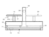
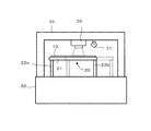
本発明に係る画像処理方法に従った画像処理が実行される画像処理装置は、例えば、半導体ウエーハの表面検査装置内に構成される。この表面検査装置の機構部は、図1及び図2に示すように構成される。なお、図1は、当該機構部の構成を示す側面図であり、図2はその正面図である。 An image processing apparatus that performs image processing according to the image processing method according to the present invention is configured, for example, in a semiconductor wafer surface inspection apparatus. The mechanism part of this surface inspection apparatus is configured as shown in FIGS. FIG. 1 is a side view showing the configuration of the mechanism, and FIG. 2 is a front view thereof.
図1及び図2において、この表面検査装置は、基台50を有し、基台50内にキャリッジ60とシフト移動機構70とが設けられている(特に図1参照)。シフト移動機構70は、ステージ71を有し、キャリッジ60がステージ71上で自走による往復移動(図1における左右方向移動、図2における紙面に垂直な方向)可能となっている。シフト移動機構70は、また、モータ、ギア機構等を含む駆動部72を有し、この駆動部72によってステージ71がキャリッジ60の自走による移動方向に直交する方向(図2における左右方向、図1における紙面に垂直な方向)に移動可能となっている。
1 and 2, the surface inspection apparatus includes a
キャリッジ60には、検査対象となる半導体ウエーハ(以下、単にウエーハという)10を支持する支持機構20が設けられ、この支持機構20が基台50の上面から突出している。支持機構20は、ウエーハ10がセットされる円形のテーブル21と、キャリッジ60の移動方向に直交する方向に沿って並んでテーブル21を支持する2つの支持脚22a、22bとを有しており、これら支持脚22a、22bがキャリッジ60に固定されている。なお、図示してはいないが、基台50の上面には、キャリッジ60の自走移動に際して、支持脚22a、22bを当該移動方向にガイドするガイド機構が設けられており、また、シフト移動機構70によってキャリッジ60がその自走方向に直交する方向にシフト移動する際に、支持脚22a、22bをその方向にガイドするシフトガイド機構が設けられている。
The
基台50上面のキャリッジ60の自走方向における略中央部に、アーチ形状のフレーム55が設けられている。このフレーム55の略中央部にはカメラユニット30が下方に向けて設けられている。また、フレーム55のカメラユニット30の設置位置近傍には照明ユニット31が設けられている。照明ユニット31は、フレーム55の下方を移動する支持機構20に支持されたウエーハ10の表面を照明する。
An arch-shaped
カメラユニット30は、ラインセンサ(例えば、1次元CCDイメージセンサ)を有しており、キャリッジ60の移動に伴って移動する支持機構20によって支持されたウエーハ10の表面を撮影する。具体的には、図3に示すように、カメラユニット30は、4回の走査によりウエーハ10の表面全体を撮影する。
The
図3において、まず、シフト初期位置Ps1において、キャリッジ60が方向A1に移動する際にカメラユニット30がウエーハ10表面の所定幅(ラインセンサの長さに対応)を方向S1に走査する。シフト初期位置Ps1での走査が完了すると、キャリッジ60がシフト移動機構70によって方向Bにシフト位置Ps2までシフトされる。次いで、シフト位置Ps2において、キャリッジ60が前記方向A1とは逆の方向A2に移動する際にカメラユニット30がウエーハ10を方向S2(方向S1と逆)に走査する。シフト位置Ps2での走査が完了すると、キャリッジ60がシフト機構70によって更に方向Bにシフト位置Ps3までシフトされる。そして、シフト位置Ps3において、キャリッジ60が方向A1に移動する際にカメラユニット30がウエーハ10を方向S1に走査する。シフト位置Ps3での走査が完了すると、キャリッジがシフト機構70によって更にシフト位置Ps4にシフトされる。このシフト位置Ps4において、キャリッジ60が方向A2に移動する際にカメラユニット30がウエーハS2方向に走査する。このように、キャリッジ60が、自走による方向A1、A2の往復動を行いつつ、シフト移動機構70による方向Bへのシフト移動を繰り返す間に、カメラユニット30がウエーハ10の表面を4回走査する。その過程で、カメラユニット30は、ウエーハ10の表面を撮影し、画像信号を順次出力する。
In FIG. 3, first, when the
表面検査装置の制御系は、図4に示すように構成されている。 The control system of the surface inspection apparatus is configured as shown in FIG.
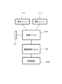
図4において、処理ユニット100は、前述したカメラユニット30からの画像信号を入力し、その画像信号をウエーハ10の表面画像を表す情報として処理する。また、処理ユニット100には駆動制御ユニット120が接続されており、駆動制御ユニット120が処理ユニット100の制御のもと、前述したキャリッジ60及びシフト移動機構70を含む移動機構200の駆動制御を行う。更に、処理ユニット100には操作ユニット111及び表示ユニット112が接続されている。ユーザによって操作される操作ユニット111からの操作信号を入力する処理ユニット100は、その操作信号に基づいた各種の処理を実行する。処理ユニット100は、処理によって得られた画像データに基づいて表示ユニット112にウエーハ10の表面画像を含む撮影画像を表示させる等、各種の情報を表示ユニット112に表示させる。
In FIG. 4, the
次に、ウエーハ10表面の欠陥を検出する処理について説明する。
Next, processing for detecting defects on the surface of the
まず、ウエーハ10の表面画像の画像処理に係る各種情報の登録に関する処理(登録処理)が行われる。
First, processing (registration processing) related to registration of various information related to image processing of the surface image of the
検査対象となるウエーハを代表するウエーハ10の表面が前述した機構部(図1〜図3参照)においてカメラユニット30によって撮影され、カメラユニット30からの画像信号を入力する処理ユニット100が図5に示す手順に従って処理を実行する。
FIG. 5 shows a
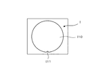
図5において、処理ユニット100は、カメラユニット30から順次供給される画像信号を画素単位の濃淡値で構成される画像データに変換し、ウエーハ10の表面全体を表すウエーハ表面画像(データ)を含む撮影画像を被処理画像として取得する(S1)。このウエーハ表面画像を含む撮影画像は画像メモリ(図示略)に展開される。処理ユニット100は、例えば、図6Aに示すように、ウエーハ表面画像I10を含む撮影画像(被処理対象画像)Iを取得すると、その撮影画像Iを画像メモリ上においてX(横方向座標軸)、Y(縦方向座標軸)及びθ(反時計方向回りの角度)の各基準に基づいて位置補正する(S2)。例えば、図6Bに示すように、ウエーハ表面画像I10のノッチ部分I11が所定の方向に位置づけられるように位置補正される。処理ユニット100は、前記位置補正されたウエーハ表面画像I10を含む撮影画像Iを表示ユニット112に表示させる。
In FIG. 5, the
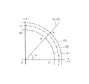
表示ユニット112に表示された撮影画像Iに対して、ユーザは、操作ユニット111を操作して、例えば、図6Cに示すように、ウエーハ表面画像I10の縁Edgに沿う円形線C0(縁線:一転鎖線参照)を設定する。円形線C0が設定された状態で操作ユニット111にて所定の決定操作がなされると、処理ユニット100は、設定された前記円形線C0の半径R及びその中心Oの位置(Xo,Yo)を取得する(S3)。次いで、処理ユニット100は、図7に示すように、半径R及びその中心Oの位置(Xo,Yo)にて特定される前記円形線C0と同心となって、半径(R−L1)の内側円形区画線C1と、前記円形線C0と同心となって、半径(R+L2)の外側円形区画線C2とを設定する。これにより、処理ユニット100は、前記円形線C0を挟んでそれに平行な前記内側円形区画線C1と前記外側円形区画線C2とによって区画されて、前記円形線C0からウエーハ表面画像I10の内側に幅L1となり、その外側に幅L2となるリング状領域ELingを認識し、撮影画像Iにおけるそのリング状領域ELing内の画像を縁部画像IEとして特定する(S4)。なお、L1、L2は、例えば、ユーザの操作ユニット11の操作により設定される。
For the captured image I displayed on the
次に、処理ユニット100は、リング状領域ELingの縁部画像IEをその幅(L1+L2)に相当する幅となる矩形画像IRに変換するために用いられるべき変換テーブル(HLUT)を作成する(S5)。この変換テーブル(HLUT)は、外周2π(R+L2)(外側円形区画線C2の長さ)及び内周2π(R−L1)(内側円形区画線C1の長さ)のリング状となる縁部画像IEの各位置を、図8に示すような、前記縁部画像IEの外周2π(R+L2)及び幅(L1+L2)に相当する長さ及び幅の矩形画像IRの画素Pxに対応付けるものである。具体的には、図9に示すように、リング状の縁部画像IEにおける第1角度範囲(0°≦θ<90°)の第1縁部画像部分IE(1)の各位置が、長さ2π(R+L2)のうちの前記第1角度範囲(0°≦θ<90°)に相当する長さの第1矩形画像部分IR(1)の画素に対応づけられ、縁部画像IEにおける第2角度範囲(90°≦θ<180°)の第2縁部画像部分IE(2)の各位置が、同様に前記第2角度範囲(90°≦θ<180°)に相当する長さの第2矩形画像部分IR(2)の画素に対応付けられる。また、リング状の縁部画像IEにおける第3角度範囲(180°≦θ<270°)の第3縁部画像部分IE(3)の各位置が、前記長さ2π(R+L2)のうちの前記第3角度範囲(180°≦θ<270°)に相当する長さの第3矩形画像部分IR(3)の画素に対応付けられ、更に、縁部画像IEにおける第4角度範囲(270°≦θ<360°,0°)の第4縁部画像部分IE(4)の各位置が、同様に前記第4角度範囲(270°≦θ<360°,0°)に相当する長さの第4矩形画像部分IR(4)の画素に対応付けられる。
Next, the
前記変換テーブルは、矩形画像IRの各画素に対応する前記縁部画像IEの位置を表すものであって、次のようにして作成される。 The conversion table represents the position of the edge image IE corresponding to each pixel of the rectangular image IR, and is created as follows.
図10A及び図10Bに示すような外周縁(外側円形区画線C2)及び内周縁(内側円形区画線C1)を有するリング形状の縁部画像IEにおいて、図11Aに示すように、その外周縁(外側円形区画線C2)に沿って等間隔δ(1画素の分解能に基づいた単位長)にn箇所の位置P0(X0,Y0)、P1(X1,Y1)、・・・Pi(Xi,Yi)、・・・、Pn-1(Xn-1,Yn-1)が決められる。なお、n=2π(R+L2)/δである。次に、図10A、図10Bおよび図11Bに示すように、外周縁(外側円形区画線C2)に設定された前記各位置Pjを通り、外周縁(外側円形区画線C2)及び内周縁(内側円形区画線C1)に直交する直線(以下、法線という)NL(θ)が設定されると、その法線NL(θ)上の前記外周縁(C2)との交点Aと前記内周縁(C1)との交点Bとの間に等間隔(δ)にm箇所の位置Pj1Δ〜PjmΔが設定され得る。なお、m=(L1+L2)/δである。具体的には、図12に示すように、法線NL(θ)上に、A点の位置PjからX方向に順次ΔXj(=δ・cosθ)ずつ、及びY方向に順次ΔYj(=δ・sinθ)ずつずれた各位置Pj1Δ〜PjmΔが点Bに至るまで設定され得る。各位置の座標値は、Pj(Xj,Yj)、Pj1Δ(Xj−ΔXj,Yj−ΔYj)、・・・、PjmΔ(Xj−mΔXj,Yj−mΔYj)である。 In the ring-shaped edge image IE having an outer peripheral edge (outer circular division line C2) and an inner peripheral edge (inner circular division line C1) as shown in FIG. 10A and FIG. 10B, as shown in FIG. N positions P 0 (X 0 , Y 0 ), P 1 (X 1 , Y 1 ) at equal intervals δ (unit length based on the resolution of one pixel) along the outer circular division line C2),. P i (X i , Y i ),..., P n-1 (X n-1 , Y n-1 ) is determined. Note that n = 2π (R + L2) / δ. Next, as shown in FIG. 10A, FIG. 10B, and FIG. 11B, it passes through each position P j set on the outer peripheral edge (outer circular division line C2), and the outer peripheral edge (outer circular division line C2) and inner peripheral edge ( When a straight line (hereinafter referred to as a normal line) NL (θ) orthogonal to the inner circular partition line C1) is set, the intersection A with the outer peripheral edge (C2) on the normal line NL (θ) and the inner peripheral edge M positions P j1Δ to P jmΔ can be set at equal intervals (δ) between the intersection B with (C1). Note that m = (L1 + L2) / δ. Specifically, as shown in FIG. 12, on the normal NL (θ), ΔX j (= δ · cos θ) sequentially from the position P j of the point A in the X direction and ΔY j ( Each position P j1Δ to P jmΔ shifted by = δ · sin θ) can be set until the point B is reached. The coordinate values of each position are P j (X j , Y j ), P j1Δ (X j −ΔX j , Y j −ΔY j ),..., P jmΔ (X j −mΔX j , Y j −mΔY j ).
前述したように縁部画像IEに設定される各位置が図8に示す矩形画像IRの画素に対応付けられる。具体的には、図13に示すように、縁部画像IEの外周縁(外側円形区画線C2)に対応した矩形画像IRの辺V(C2)に沿って並ぶn個の各画素Px0〜Pxn-1が、縁部画像IEの外周縁(外側円形区画線C2)に沿って設定された位置P0(X0,Y0)〜Pn-1(Xn-1,Yn-1)に対応付けられ、矩形画像IRの前記辺V(C2)から1画素分内側に並ぶn個の画素Px01〜Px(n-1)1が、縁部画像IEの外周縁(外側円形区画線C2)から間隔δだけ内側に設定された位置P01Δ(X0−ΔX0,Y0−ΔY0)〜P(n-1)1Δ(Xn-1−ΔXn-1,Yn-1−ΔYn-1)に対応付けられ、以下、同様にして、縁部画像IEの内周縁(内側円形区画線C1)に対応した矩形画像IRの辺V(C1)に沿って並ぶn個の各画素Px0m〜Px(n-1)mが、縁部画像IEの内周縁(内側円形区画線C1)に沿って設定された位置P0mΔ(X0−mΔX0,Y0−mΔY0)〜P(n-1)mΔ(Xn-1−mΔXn-1,Yn-1−mΔYn-1)に対応付けられる。 As described above, each position set in the edge image IE is associated with a pixel of the rectangular image IR shown in FIG. Specifically, as shown in FIG. 13, each of the n pixels Px 0 to Px 0 aligned along the side V (C2) of the rectangular image IR corresponding to the outer peripheral edge (outer circular division line C2) of the edge image IE. Positions P 0 (X 0 , Y 0 ) to P n-1 (X n-1 , Y n- ) where Px n-1 is set along the outer peripheral edge (outer circular division line C2) of the edge image IE. 1 ), n pixels Px 01 to Px (n−1) 1 that are aligned by one pixel from the side V (C2) of the rectangular image IR are the outer peripheral edge (outer circular shape ) of the edge image IE. Positions P 01Δ (X 0 −ΔX 0 , Y 0 −ΔY 0 ) to P (n−1) 1Δ (X n−1 −ΔX n−1 , Y n ) set inward by the interval δ from the lane marking C 2) −1− ΔY n−1 ), and n similarly arranged along the side V (C1) of the rectangular image IR corresponding to the inner peripheral edge (inner circular division line C1) of the edge image IE. number of pixels Px 0m ~Px (n-1) m Inner peripheral edge position P 0Emuderuta set along the (inner circular partition line C1) of the edge image IE (X 0 -mΔX 0, Y 0 -mΔY 0) ~P (n-1) mΔ (X n-1 −mΔX n−1 , Y n−1 −mΔY n−1 ).
変換テーブル(HLUT)は、上述した関係を考慮して、図14に示すように、矩形画像IRにおける幅方向1列分の画素(Px0〜Px0m)、(Px1〜Px1m)、・・・・、(Pxn-1〜Px(n-1)m)に対して、縁部画像IEの外周縁(外側円形区画線C2)に沿って設定された各位置P0〜Pn-1の座標値を含む数値(X0,Y0,ΔX0,ΔY0)、(X1,Y1,ΔX1,ΔY1)、・・・、(Xn-1,Yn-1,ΔXn-1,ΔYn-1)が対応付けられている。このような変換テーブル(HLUT)を用いることにより、矩形画像IRにおいて幅方向に並ぶ1列目の各画素(Px0〜Pxom)に対応する縁部画像IEの各位置が、(X0,Y0)、(X0−ΔX0,Y0−ΔY0)、・・・、(X0−mΔX0,Y0−mΔY0)のように決められ、同様に、幅方向に並ぶ任意の(i+1)列目の各画素(Pxi〜Pxim)に対応する縁部画像IEの各位置が、(Xi,Yi)、(Xi−ΔXi,Yi−ΔYi)、・・・、(Xi−mΔXi,Yi−mΔYi)のように決められる。
In consideration of the above-described relationship, the conversion table (HLUT) includes pixels (Px 0 to Px 0m ), (Px 1 to Px 1m ), (Px 1 to Px 1m ), one column in the width direction in the rectangular image IR, as shown in FIG. ..., (Px n-1 to Px (n-1) m ), positions P 0 to P n- set along the outer peripheral edge (outer circular division line C2) of the edge image IE. numerical containing one coordinate
変換テーブル(HLUT)が、図13に示すような縁部画像IEに設定された全位置と矩形画像IRの各画素との対応関係ではなく、図14に示すように、矩形画像IRの幅方向の画素1列分に、縁部画像IEにおける外縁線(外側円形区画線C2)に沿った各位置P0(X0,Y0)〜Pn-1(Xn-1,Yn-1)と該各位置を通る法線上に設定された位置の間隔Δとに対応づけるようにしているので、変換テーブル(HLUT)をより小規模に構成することができ、結果として、それを記憶するメモリの容量を削減することができるようになる。 The conversion table (HLUT) is not the correspondence between all the positions set in the edge image IE and each pixel of the rectangular image IR as shown in FIG. 13, but the width direction of the rectangular image IR as shown in FIG. Positions P 0 (X 0 , Y 0 ) to P n-1 (X n-1 , Y n-1 ) along the outer edge line (outer circular division line C2) in the edge image IE. ) And the position interval Δ set on the normal line passing through each position, the conversion table (HLUT) can be configured on a smaller scale, and as a result, it is stored. The memory capacity can be reduced.
図5に戻って、前述したような関係にて矩形画像IRの各画素に対応する縁部画像IEの位置を表す変換テーブル(HLUT)が生成されると、処理ユニット100は、逆に、縁部画像IEの各画素に対応する矩形画像IRの位置を表す逆変換テーブル(NLUT)を生成する(S6)。図8に示すような、長さ2π(R+L2)で幅(L1+L2)に相当する長さ及び幅の矩形画像IRの各位置を、外周2π(R+L2)及び内周2π(R−L1)の元のリング状領域ELingの画像(縁部画像IE)の画素に対応付けるものである。具体的には、図15に示すように、長さ2π(R+L2)のうちの第1角度範囲(0°≦θ<90°)に相当する長さの第1矩形画像部分IR(1)の各位置を、リング状の縁部画像IEにおける前記第1角度範囲(0°≦θ<90°)の第1縁部画像部分IE(1)の各画素に対応付け、同様に第2角度範囲(90°≦θ<180°)に相当する長さの第2矩形画像部分IR(2)の各位置を、縁部画像IEにおける前記第2角度範囲(90°≦θ<180°)の第2縁部画像部分IE(2)の画素に対応付ける。前記逆変換テーブルは、また、長さ2π(R+L2)のうちの第3角度範囲(180°≦θ<270°)に相当する長さの第3矩形画像部分IR(3)の各位置を、リング状の縁部画像IEにおける前記第3角度範囲(180°≦θ<270°)の第3縁部画像部分IE(3)の画素に対応付け、更に、第4角度範囲(270°≦θ<360°,0°)に相当する長さの第4矩形画像部分IR(4)の各位置を、縁部画像IEにおける前記第4角度範囲(270°≦θ<360°,0°)の第4縁部画像部分IE(4)の画素に対応づける。
Returning to FIG. 5, when a conversion table (HLUT) representing the position of the edge image IE corresponding to each pixel of the rectangular image IR is generated in the relationship as described above, the
なお、この逆変換テーブル(NLUT)の生成手法は、前述した変換テーブル(HLUT)のものと同様である。 The method for generating the inverse conversion table (NLUT) is the same as that of the conversion table (HLUT) described above.
前記変換テーブル(HLUT)と前記逆変換テーブル(NLUT)とが生成されると、処理ユニット100は、前記変換テーブル(HLUT)を用いてウエーハ表面画像I10を含む撮影画像Iにおいて特定された縁部画像IEを矩形画像IRに変換し、更に、前記逆変換テーブル(NLUT)を用いて前記変換により得られた矩形画像IRを元のリング状領域ELingの画像(縁部画像IE)に逆変換する(S7)。そして、その逆変換にて得られた画像を含む撮影画像Iが表示ユニット112に表示される。ユーザは、表示ユニット112に表示された撮影画像Iの特に前記リング状領域ELingの画像部分に問題がなければ、操作ユニット111で所定の登録実行の操作を行う。処理ユニット100は、操作ユニット111からの登録実行の操作に基づいた操作信号を入力すると、前述したように設定したウエーハ表面画像I10の縁に沿った円形線C0(縁線)を特定するための中心位置O(Xo,Yo)及び半径(R)、リング状領域ELingの境界線(C1、
)を表す円形線C0からの幅L1、L2、変換テーブル(HLUT)、逆変換テーブル(NLUT)及びウエーハ表面画像I10の円形領域から前記リング状領域ELing除いた中心位置(Xo,Yo)、半径(R−L1)の円形本体部領域を内部メモリに登録して(S8)、処理を終了する。この登録処理は、検査を行うウエーハの直径別に行うことができる。
When the conversion table (HLUT) and the inverse conversion table (NLUT) are generated, the
) From the circular line C0 representing the center line (Xo, Yo) obtained by removing the ring-shaped region E Ling from the circular region of the conversion table (HLUT), inverse conversion table (NLUT), and wafer surface image I10. The circular main body region having the radius (R-L1) is registered in the internal memory (S8), and the process is terminated. This registration process can be performed for each diameter of the wafer to be inspected.
なお、ユーザは、前記変換及び逆変換の処理を経て得られた撮影画像Iの特に前記リング状領域ELingの画像部分に何らかの問題があれば、再度、ウエーハ10の表面を撮影して、ウエーハ表面画像I10に対する円形線C0及び幅L1、L2を決め、変換テーブル(HLUT)、逆変換テーブル(NLUT)を生成することができる。
If there is any problem in the image portion of the captured image I obtained through the conversion and inverse conversion, particularly in the ring-shaped region E Ling , the user again captures the surface of the
前述したようにして登録処理が終了した後に、当該表面検査装置は、各ウエーハ10の表面検査を行うことができる。検査対象となるウエーハ10の表面が前述した機構部(図1〜図3参照)においてカメラユニット30によって撮影され、カメラユニット30からの画像信号を入力する処理ユニット100が図16に示す手順に従って処理を実行する。
After the registration process is completed as described above, the surface inspection apparatus can perform the surface inspection of each
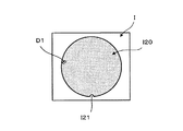
図16において、処理ユニット100は、検査対象となるウエーハ10の表面を撮影するカメラユニット30から順次供給される画像信号を画素単位の濃淡値で構成される画像データに変換し、ウエーハ10の表面全体を表すウエーハ表面画像(データ)を含む撮影画像を被処理画像として取得する(S11)。このウエーハ表面画像を含む被処理画像は画像メモリ(図示略)に展開される。処理ユニット100は、例えば、図17Aに示すようなウエーハ表面画像I20を含む撮影画像Iを取得すると、その撮影画像Iを画像メモリ上においてX(横方向座標軸)、Y(縦方向座標軸)及びθ(反時計方向回りの角度)の各基準に基づいて位置補正する(S12)。例えば、図17Bに示すように、ウエーハ表面画像I20のノッチ部分I21が所定の方向に位置づけられるとともに、ウエーハ表面画像I20が、登録処理の際のもの(図5、図6B参照)と同様に位置づけられるように位置補正され、その位置補正後の撮影画像Iが画像メモリ上に展開される。なお、この場合、ウエーハ表面画像I20の外縁部分に欠陥部分D1がある。
In FIG. 16, the
処理ユニット100は、前記登録された円形線C0を特定するその中心位置(Xo,Yo)及び半径(R)、及びリング状領域ELingを特定する幅L1、L2に基づいて、位置補正されたウエーハ表面画像I20において、検査エリアのマッピングを行う(S13)。このマッピングにより、リング状領域ELingの画像が縁部画像IEとして特定されるとともに、ウエーハ表面画像I20の領域から前記リング状領域ELing(縁部画像IE)を除いた円形本体部領域(半径(R−L1)のウエーハ本体部画像)が特定される。
The
次いで、処理ユニット100は、前記マッピングによって得られたリング状領域ELingの画像である縁部画像IEを前述した変換テーブル(HLUT)(図13、図14参照)を用いて矩形画像IRに変換する(S14)。この変換の処理において、まず、矩形画像IRの各画素(図8参照)に対応するリング状の縁部画像IEにおける位置が前記変換テーブル(HLUT)から取得される。次いで、取得された前記縁部画像IEにおける位置の濃淡値が取得され、その濃淡値が当該位置に対応する矩形画像IRの画素の濃淡値として決められる。前記縁部画像IEにおける位置が当該縁部画像IEにおける画素位置に合致する場合、当該画素の濃淡値が対応する矩形画像IRにおける画素の濃淡値として決められる。また、前記縁部画像IEにおける位置が当該縁部画像IEの画素位置に合致しない場合、当該位置の周辺画素の濃淡値による補間処理により当該位置の濃淡値が決定され、その濃淡値が対応する矩形画像IRの画素の濃淡値として決められる。
Next, the
このようにして、矩形画像IRにおける各画素の濃淡値が変換テーブル(HLUT)により対応付けられた縁部画像IEにおける位置の濃淡値に決められることにより、前記縁部画像IEが前記矩形画像IRに変換される。この変換処理により、図18に示すように、縁部画像IEにおける第1角度範囲(0°≦θ<90°)の第1縁部画像部分IE(1)が、長さ2π(R+L2)のうちの前記第1角度範囲(0°≦θ<90°)に相当する長さの第1矩形画像部分IR(1)に変換され、縁部画像IEにおける第2角度範囲(90°≦θ<180°)の第2縁部画像部分IE(2)が、同様に前記第2角度範囲(90°≦θ<180°)に相当する長さの第2矩形画像部分IR(2)に変換される。また、リング状の縁部画像IEにおける第3角度範囲(180°≦θ<270°)の第3縁部画像部分IE(3)が、前記長さ2π(R+L2)のうちの前記第3角度範囲(180°≦θ<270°)に相当する長さの第3矩形画像部分IR(3)に変換され、更に、縁部画像IEにおける第4角度範囲(270°≦θ<360°,0°)の第4縁部画像部分IE(4)が、同様に前記第4角度範囲(270°≦θ<360°,0°)に相当する長さの第4矩形画像部分IR(4)に変換される。この場合、第2縁部画像部分IE(2)に存在する欠陥部分D1は、対応する第2矩形画像部分IR(2)の欠陥部分DR1に変換される。 In this way, the gray value of each pixel in the rectangular image IR is determined as the gray value of the position in the edge image IE associated with the conversion table (HLUT), so that the edge image IE becomes the rectangular image IR. Is converted to By this conversion processing, as shown in FIG. 18, the first edge image portion IE (1) in the first angle range (0 ° ≦ θ <90 °) in the edge image IE has a length of 2π (R + L2). The first rectangular image portion IR (1) having a length corresponding to the first angular range (0 ° ≦ θ <90 °) is converted into the second angular range (90 ° ≦ θ <in the edge image IE). 180 °) second edge image portion IE (2) is similarly converted into a second rectangular image portion IR (2) having a length corresponding to the second angle range (90 ° ≦ θ <180 °). The Further, the third edge image portion IE (3) in the third angle range (180 ° ≦ θ <270 °) in the ring-shaped edge image IE is the third angle of the length 2π (R + L2). It is converted into a third rectangular image portion IR (3) having a length corresponding to the range (180 ° ≦ θ <270 °), and further, the fourth angular range (270 ° ≦ θ <360 °, 0 in the edge image IE). The fourth edge image portion IE (4) at the same angle is the fourth rectangular image portion IR (4) having a length corresponding to the fourth angle range (270 ° ≦ θ <360 °, 0 °). Converted. In this case, the defect portion D1 present in the second edge image portion IE (2) is converted into the defect portion DR1 of the corresponding second rectangular image portion IR (2).
図16に戻って、処理ユニット100は、矩形画像IRを生成すると、その矩形画像IRに対して欠陥部分を強調するために1次元フィルタ処理を施す(S15)。この1次元フィルタ処理では、各注目画素の濃淡値が、その注目画素に対して矩形画像IRの幅方向に直交する方向、即ち、縁部画像IEの縁線として設定された円形線C0に対応する横方向に延びる直線V(C0)(図8参照)と平行となる方向において前後に並ぶ画素の濃淡値に基づいて決められる。このような1次元フィルタ処理により、欠陥部分が強調された状態の処理済矩形画像IRPが得られる。具体的には、図19に示すように、第1角度範囲(0°≦θ<90°)に対応する第1矩形画像部分IR(1)から同角度範囲に対応する第1処理済矩形画像IRP(1)が生成され、第2角度範囲(90°≦θ<180°)に対応する第2矩形画像部分IR(2)から同角度範囲に対応する第2処理済矩形画像IRP(2)が生成され、第3角度範囲(180°≦θ<270°)に対応する第3矩形画像部分IR(3)から同角度範囲に対応する第3処理済矩形画像IRP(3)が生成され、更に、第4角度範囲(270°≦θ<360°,0°)に対応する第4矩形画像部分IR(4)から同角度範囲に対応する第4処理済矩形画像IRP(4)が生成される。この場合、第2矩形画像部分IR(2)に含まれた欠陥部分DR1は強調されて、欠陥部分DR1Pとして第2処理済矩形画像部分IRP(2)に生成されている。
Returning to FIG. 16, when the
矩形画像IRに対して1次元フィルタ処理が施されて処理済矩形画像IRPが得られると、処理ユニット100は、逆変換テーブル(NLUT)を用いて処理済矩形画像IRPを元のリング状領域ELingの画像に逆変換する(S16)。この逆変換の処理において、まず、元のリング状領域ELingの各画素に対応する処理済矩形画像IRPの位置が前記逆変換テーブル(NLUT)から取得される。次いで、取得された前記処理済矩形画像IRPにおける位置の濃淡値が取得され、その濃淡値が当該位置に対応するリング状領域ELingにおける画素の濃淡値として決められる。前記処理済矩形画像IRPにおける位置が当該処理済矩形画像IRPにおける画素位置に合致する場合、当該画素の濃淡値が対応するリング状領域ELingの画素の濃淡値として決められる。また、前記処理済矩形画像IRPにおける位置が当該処理済矩形画像IRPにおける画素位置に合致しない場合、当該位置の周辺画素の濃淡値による補間処理により当該位置の濃淡値が決定され、その濃淡値が対応するリング状領域ELingにおける画素の濃淡値として決められる。
When the rectangular image IR is subjected to the one-dimensional filter processing to obtain the processed rectangular image IR P , the
このようにして、リング状領域ELingの各画素の濃淡値が逆変換テーブル(NLUT)により対応付けられた処理済矩形画像IRPの位置の濃淡値に決められることにより、前記処理済矩形画像IRPが前記リング状領域ELingの画像に変換され、処理済縁部画像IEPが得られることになる。この逆変換処理により、図20に示すように、第1角度範囲(0°≦θ<90°)に対応する第1処理済矩形画像部分IRP(1)が、同角度範囲の第1処理済縁部画像部分IEP(1)に逆変換され、第2角度範囲(90°≦θ<180°)に対応する第2処理済矩形画像部分IRP(2)が、同角度範囲の第2処理済縁部画像部分IEP(2)に変換され、第3角度範囲(180°≦θ<270°)に対応する第3処理済矩形画像部分IRP(3)が、同角度範囲の第3処理済縁部画像部分IEP(3)に変換され、更に、第4角度範囲(270°≦θ<360°,0°)に対応する第4処理済矩形画像部分IRP(4)が、同角度範囲の第4処理済縁部画像部分IEP(4)に変換される。この場合、第2処理済矩形画像部分IRP(2)に強調されて写り込んでいる欠陥部分DR1Pは第2処理済縁部画像IEP(2)において強調された欠陥部分D1Pに変換される。 In this way, by being determined to gray value of the position of the processed rectangular image IR P associated with gray value of each pixel of the ring-shaped region E Ling inverse conversion table (NLUT), the processed rectangular image The IR P is converted into an image of the ring-shaped region E Ling , and a processed edge image IE P is obtained. As a result of this inverse transformation processing, as shown in FIG. 20, the first processed rectangular image portion IR P (1) corresponding to the first angular range (0 ° ≦ θ <90 °) is converted into the first processing within the same angular range. The second processed rectangular image part IR P (2) corresponding to the second angle range (90 ° ≦ θ <180 °) is inversely transformed into the finished edge image part IE P (1), 2 The processed edge image portion IE P (2) is converted into a third processed rectangular image portion IR P (3) corresponding to the third angle range (180 ° ≦ θ <270 °). The fourth processed rectangular image portion IR P (4) converted to the third processed edge image portion IE P (3) and further corresponding to the fourth angle range (270 ° ≦ θ <360 °, 0 °). Is converted into the fourth processed edge image portion IE P (4) in the same angle range. In this case, the defect portion DR1 P highlighted in the second processed rectangular image portion IR P (2) is converted into the defect portion D1 P emphasized in the second processed edge image IE P (2). Is done.
図16に戻って、処理ユニット100は、前述した処理済縁部画像IEPの生成に次いで、前記マッピング(S13参照)により得られたウエーハ表面画像I20の領域から前記リング領域ELingを除いた円形本体部領域の画像に対して2次元フィルタ処理を施す(S17)。具体的には、円形本体部領域の画像(ウエーハ本体部画像)において、各注目画素の濃淡値が、2次元的に配置されるその周辺画素(例えば、注目画素を囲む8画素)の濃淡値に基づいて決められる。このような2次元フィルタ処理が施されることにより、処理済ウエーハ本体部画像が得られる。この処理済ウエーハ本体部画像においては、欠陥部分が強調された状態となる。次に、処理ユニット100は、前記処理済縁部画像IEPと前記処理済ウエーハ本体部画像とを合成し、単一の処理済ウエーハ表面画像I20Pを生成する(S18)。そして、処理ユニット100は、生成された処理済ウエーハ表面画像I20Pに対して欠陥検出処理を施す(S19)。例えば、処理済ウエーハ表面画像I20Pの濃度分布に基づいて欠陥部分が特定される。処理ユニット100は、前記欠陥検出処理により得られた欠陥部分を特定する情報、即ち、欠陥情報(例えば、欠陥番号(NO.),欠陥部分の中心座標、欠陥部分の面積、欠陥部分の扁平度、欠陥部分を近似する楕円の長軸及び短軸、欠陥分類番号(NO.)等)を生成し、該欠陥情報を前記処理済ウエーハ表面画像I20Pとともに保存する(S20)。そして、処理ユニット100は、図21に示すように、前記欠陥情報にて特定される欠陥部分D1P、D2P、D3P、D4Pを処理済ウエーハ表面画像I20Pとともに表示ユニット112に表示させる。なお、図21において、欠陥部分D1Pは、前記処理済縁部画像IEP上で特定されたものであり、他の欠陥部分D2P、D3P及びD4Pは、前記処理済ウエーハ本体部画像上で特定されたものである。
Returning to FIG. 16, the
前述したウエーハの表面検査装置にてなされる画像処理では、撮影画像I(被処理画像)において特定されたウエーハ表面画像I10の縁に沿った円形線C0を含む縁部画像IEが矩形画像IRに変換され、その矩形画像IRに対して1次元フィルタ処理が施される。この1次元フィルタ処理が、ウエーハ表面画像I20の縁に対して設定された円形線Co対応する直線V(Co)に沿った方向での処理になるので、その1次元フィルタ処理の施された処理済矩形画像IRPが逆変換されて得られる処理済縁部画像IEPは、実質的に前記ウエーハ表面画像I20の縁線に沿ってフィルタ処理が施されたものとなる。従って、ウエーハ表面画像I20の縁部分の領域において適正なフィルタ処理の施された画像(処理済縁部画像IEP)を容易に得ることができるようになる。 In the image processing performed by the wafer surface inspection apparatus described above, the edge image IE including the circular line C0 along the edge of the wafer surface image I10 specified in the photographed image I (image to be processed) is converted into the rectangular image IR. After the conversion, the one-dimensional filter process is performed on the rectangular image IR. Since this one-dimensional filter process is a process in the direction along the straight line V (Co) corresponding to the circular line Co set with respect to the edge of the wafer surface image I20, the process subjected to the one-dimensional filter process processing Sumien unit image IE P obtained already rectangular image IR P is inverse transform becomes the filter along the edge lines of substantially the wafer surface image I20 is applied. Accordingly, it is possible to easily obtain an image (processed edge image IE P ) that has been subjected to appropriate filtering in the region of the edge portion of the wafer surface image I20.
また、ウエーハ表面画像I20の縁部分の領域において適正なフィルタ処理の施された画像(処理済縁部画像IEP)が得られるので、ウエーハ表面画像I20の縁部分にある欠陥部分D1pも、その内側のウエーハ本体部画像にある欠陥部分D2P、D3P、D4Pと同様に適確に検出することができるようになる。 In addition, since an image (processed edge image IE P ) that has been appropriately filtered is obtained in the region of the edge portion of the wafer surface image I20, the defect portion D1 p in the edge portion of the wafer surface image I20 is also obtained. Like the defective portions D2 P , D3 P , and D4 P in the inner wafer main body image, it can be accurately detected.
なお、前述した本発明の実施の形態では、ウエーハ表面画像I20に設定された縁線としての円形線C0を含むリング状領域ELing内の画像を縁部画像IEとしたが、そのリング領域ELingの一部の画像を縁部画像IEとして処理することも可能である。また、物体表面の縁線が円形ではなく、任意の曲線であっても、その縁の曲線に沿った縁線を設定し、その縁線に直交する方向に所定幅となる領域の画像を縁部画像として特定することもできる。この場合、その任意の曲形状となる縁部画像の各位置と矩形画像の各画素との対応関係に基づいて当該縁画像が矩形画像に変換され、また、処理済矩形画像が元の曲形状の領域の画像(処理済縁部画像)に逆変換される。 In the above-described embodiment of the present invention, the image in the ring-shaped region E Ling including the circular line C0 as the edge line set in the wafer surface image I20 is the edge image IE. It is also possible to process a part of the Ling image as the edge image IE. Even if the edge line of the object surface is not a circle but an arbitrary curve, an edge line along the edge curve is set, and an image of an area having a predetermined width in the direction orthogonal to the edge line is It can also be specified as a partial image. In this case, the edge image is converted into a rectangular image on the basis of the correspondence between each position of the edge image in the arbitrary curved shape and each pixel of the rectangular image, and the processed rectangular image is converted into the original curved shape. Is converted back to an image of the region (processed edge image).
また、本発明に係る画像処理方法及び画像処理装置では、矩形画像IRに対して施される1次元画像処理は、フィルタ処理に限られず、矩形画像IRの幅方向に直交する方向に並ぶ複数画素の濃淡値を順次処理する1次元画像処理であれば、特に限定されない。 In the image processing method and the image processing apparatus according to the present invention, the one-dimensional image processing performed on the rectangular image IR is not limited to the filter processing, and a plurality of pixels arranged in a direction orthogonal to the width direction of the rectangular image IR. There is no particular limitation as long as it is a one-dimensional image process that sequentially processes the gray values.
前述した本発明の実施の形態では、縁部画像IEから変換された矩形画像IRに対して1次元画像処理(1次元フィルタ処理)を施して処理済み矩形画像IRPを得た後に、更に、その処理済み矩形画像IRPを逆変換して処理済み縁部画像IEPを生成し、その処理済み縁部画像IEP(実際には合成画像)において欠陥を検出している。しかし、単に、被処理画像の特に縁部画像IE内の欠陥の有無だけを検出する場合等では、処理済み矩形画像IRPを逆変換する必要なく、処理済み矩形画像IRPにおいて欠陥検出の処理を行うことができる。 In the embodiment of the present invention described above, after obtaining the processed rectangular image IR P by applying 1-dimensional image processing (1D filtering) for the converted rectangular image IR from the edge image IE, further, generating the processed rectangular image IR P inverse transform to the processed edge image IE P, it detects the defect in the processed edge image IE P (actually a composite image). However, simply in such a case to detect only particular the presence or absence of a defect in the edge image IE of the processed image, without the need to inverse transform the processed rectangular image IR P, the processing of the defect detected in the processed rectangular image IR P It can be performed.
更に、前述した本発明の実施の形態では、半導体ウエーハの撮影画像を被処理画像としたが、被処理画像は、何らかの物体の表面画像を含むものであれば特に限定されない。 Furthermore, in the above-described embodiment of the present invention, the captured image of the semiconductor wafer is the processed image, but the processed image is not particularly limited as long as it includes a surface image of some object.
以上、説明したように、本発明に係る画像処理方法及び画像処理装置は、物体表面画像の縁部分の領域において適正な画像処理済の施された画像を得ることができるという効果を有し、画素単位の濃淡値にて構成される物体表面画像を処理する画像処理方法及び画像処理装置として有用であり、表面検査装置に好適である。 As described above, the image processing method and the image processing device according to the present invention have an effect that an image subjected to appropriate image processing can be obtained in the region of the edge portion of the object surface image, It is useful as an image processing method and an image processing apparatus for processing an object surface image composed of grayscale values in pixel units, and is suitable for a surface inspection apparatus.
10 ウエーハ
20 支持機構
21 テーブル
22a、22b 支持脚
30 カメラユニット
31 照明ユニット
50 基台
55 フレーム
60 キャリッジ
70 シフト移動機構
71 ステージ
72 駆動部
100 処理ユニット
111 操作ユニット
112 表示ユニット
120 駆動制御ユニット
200 移動機構
DESCRIPTION OF
Claims (30)
前記被処理画像において設定された前記物体表面画像の縁線を含み、該縁線に直交する方向に所定幅となる領域の画像を縁部画像として特定する縁部画像特定ステップと、
前記縁部画像を前記所定幅に相当する幅の矩形画像に変換する変換ステップと、
前記矩形画像に対して、その幅方向に直交する方向に並ぶ複数画素の濃淡値を順次処理する1次元画像処理を施す画像処理ステップとを有する画像処理方法。 An image acquisition step configured to acquire an image to be processed including an object surface image, which is configured by a grayscale value in pixel units;
An edge image specifying step for specifying, as an edge image, an image of a region that includes an edge line of the object surface image set in the processed image and has a predetermined width in a direction orthogonal to the edge line;
A conversion step of converting the edge image into a rectangular image having a width corresponding to the predetermined width;
An image processing method comprising: an image processing step for performing one-dimensional image processing for sequentially processing the grayscale values of a plurality of pixels arranged in a direction orthogonal to the width direction of the rectangular image.
前記矩形画像の各画素に対応する前記縁部画像における位置を取得する位置変換ステップと、
前記縁部画像中の各画素の濃淡値に基づいて、前記取得された縁部画像における各位置に対応する前記矩形画像の画素の濃淡値を決めるステップとを有する請求項1乃至3のいずれかに記載の画像処理方法。 The converting step includes
A position conversion step of obtaining a position in the edge image corresponding to each pixel of the rectangular image;
4. A step of determining a gray value of a pixel of the rectangular image corresponding to each position in the acquired edge image based on a gray value of each pixel in the edge image. An image processing method described in 1.
前記位置変換ステップは、前記変換テーブルを用いて前記矩形画像の各画素に対応する前記縁部画像における位置を取得する請求項4記載の画像処理方法。 A conversion table representing a position in the edge image corresponding to each pixel of the rectangular image is created in advance,
The image processing method according to claim 4, wherein the position conversion step acquires a position in the edge image corresponding to each pixel of the rectangular image using the conversion table.
前記元の領域の画像の各画素に対応する矩形画像における位置を取得する位置逆変換ステップと、
前記1次元画像処理の施された矩形画像中の各画素の濃淡値に基づいて、前記取得された矩形画像における各位置に対応する前記元の領域の画像における画素の濃淡値を決めて、前記処理済縁部画像を生成するステップとを有する請求項2記載の画像処理方法。 The inverse transformation step includes
A position reverse conversion step of acquiring a position in a rectangular image corresponding to each pixel of the image of the original region;
Based on the gray value of each pixel in the rectangular image subjected to the one-dimensional image processing, the gray value of the pixel in the image of the original region corresponding to each position in the acquired rectangular image is determined, The image processing method according to claim 2, further comprising a step of generating a processed edge image.
前記位置逆変換ステップは、前記逆変換テーブルを用いて前記元の領域の画像の各画素に対応する前記矩形画像における位置を取得する請求項6記載の画像処理方法。 Create in advance an inverse conversion table representing the position in the rectangular image corresponding to each pixel of the image of the original area,
The image processing method according to claim 6, wherein the position reverse conversion step acquires a position in the rectangular image corresponding to each pixel of the image of the original region using the reverse conversion table.
前記縁部画像特定ステップは、前記半導体ウエーハ表面画像の縁に沿った円形線に直交する方向に所定幅となるリング状領域の全部または一部の画像を縁部画像として特定する請求項1記載の画像処理方法。 The image acquisition step acquires an image including a surface image of a disk-shaped semiconductor wafer as the processed image,
2. The edge image specifying step specifies all or a part of an image of a ring-shaped region having a predetermined width in a direction orthogonal to a circular line along the edge of the semiconductor wafer surface image as an edge image. Image processing method.
前記縁部画像特定ステップは、前記半導体ウエーハ表面画像の縁に沿った円形線に直交する方向に所定幅となるリング状領域の全部または一部の画像を縁部画像として特定し、
前記逆変換ステップは、前記1次元画像処理の施された前記矩形画像を元のリング状領域の全部または一部の画像に逆変換して前記処理済縁部画像を生成する請求項2記載の画像処理方法。 The image acquisition step acquires an image including a surface image of a disk-shaped semiconductor wafer as the processed image,
The edge image specifying step specifies, as an edge image, an image of all or part of a ring-shaped region having a predetermined width in a direction orthogonal to a circular line along the edge of the semiconductor wafer surface image,
3. The inverse transformation step generates the processed edge image by inversely transforming the rectangular image subjected to the one-dimensional image processing into an image of all or a part of an original ring-shaped region. Image processing method.
前記変換ステップは、前記変換テーブルを用いて、前記矩形画像の各画素に対応する前記縁部画像における位置を決定するステップを有する請求項11または12記載の画像処理方法。 A conversion table is prepared in advance for associating each position along the partition line in the edge image with one column of pixels of the rectangular image associated with all positions set on the normal passing through the position. Aside,
The image processing method according to claim 11, wherein the conversion step includes a step of determining a position in the edge image corresponding to each pixel of the rectangular image using the conversion table.
前記被処理画像を、当該被処理画像の前記平行な2つの区画線のうちの一方の区画線に沿って所定間隔にて設定された各位置及び該各位置から当該区画線に直交する法線上に他方の区画線まで所定間隔で設定された各位置に対応する矩形配列された画素からなる矩形画像に変換する変換ステップを有する画像処理方法。 An image acquisition step of acquiring an image to be processed partitioned by two parallel partition lines;
Each position of the image to be processed is set at a predetermined interval along one of the two parallel partition lines of the image to be processed, and a normal line orthogonal to the partition line from each position. An image processing method comprising a conversion step of converting to a rectangular image composed of pixels arranged in a rectangular pattern corresponding to positions set at predetermined intervals up to the other partition line.
前記変換ステップは、前記変換テーブルを用いて、前記矩形画像の各画素に対応する前記被処理画像における位置を決定するステップを有する請求項14または15記載の画像処理方法。 Create in advance a conversion table for associating each position along the partition line in the image to be processed with one column of pixels of the rectangular image associated with all positions set on the normal passing through the position. Aside,
16. The image processing method according to claim 14, wherein the conversion step includes a step of determining a position in the image to be processed corresponding to each pixel of the rectangular image using the conversion table.
該撮影手段により得られた撮影画像を処理する処理ユニットとを有し、
前記処理ユニットは、
画素単位の濃淡値により構成され、前記物体の表面画像を含む被処理画像を取得する画像取得手段と、
前記被処理画像において設定された前記物体表面画像の縁線を含み、該縁線に直交する方向に所定幅となる領域の画像を縁部画像として特定する縁部画像特定手段と、
前記縁部画像を前記所定幅に相当する幅の矩形画像に変換する変換手段と、
前記矩形画像に対して、その幅方向に直交する方向に並ぶ複数画素の濃淡値を順次処理する1次元画像処理を施す画像処理手段とを有する画像処理装置。 Photographing means for photographing the surface of the object;
A processing unit for processing a photographed image obtained by the photographing means,
The processing unit is
An image acquisition unit configured to obtain a processed image including a surface image of the object, which is configured by a grayscale value in pixel units;
Edge image specifying means for specifying, as an edge image, an image of a region including a border line of the object surface image set in the processed image and having a predetermined width in a direction orthogonal to the border line;
Conversion means for converting the edge image into a rectangular image having a width corresponding to the predetermined width;
An image processing apparatus comprising: an image processing unit that performs one-dimensional image processing for sequentially processing the grayscale values of a plurality of pixels arranged in a direction orthogonal to the width direction of the rectangular image.
前記矩形画像の各画素に対応する前記縁部画像における位置を取得する位置変換手段と、
前記縁部画像中の各画素の濃淡値に基づいて、前記取得された縁部画像における各位置に対応する前記矩形画像の画素の濃淡値を決める手段とを有する請求項17または18記載の画像処理装置。 The converting means includes
Position conversion means for acquiring a position in the edge image corresponding to each pixel of the rectangular image;
The image according to claim 17 or 18, further comprising means for determining a gray value of a pixel of the rectangular image corresponding to each position in the acquired edge image based on a gray value of each pixel in the edge image. Processing equipment.
前記位置変換手段は、前記変換テーブルを用いて前記矩形画像の各画素に対応する前記縁部画像中の位置を取得する請求項19記載の画像処理装置。 Storage means for storing a conversion table representing a position in the edge image corresponding to each pixel of the rectangular image;
The image processing apparatus according to claim 19, wherein the position conversion unit acquires a position in the edge image corresponding to each pixel of the rectangular image using the conversion table.
前記画像取得手段は、前記半導体ウエーハ表面画像を含む画像を前記被処理画像として取得し、
前記縁部画像特定手段は、前記半導体ウエーハ表面画像の縁に沿った円形線に直交する方向に所定幅となるリング状領域の全部または一部の画像を縁部画像として特定し、
前記逆変換手段は、前記1次元画像処理の施された前記矩形画像を元のリング状領域の全部または一部の画像に逆変換して処理済縁部画像を生成する請求項17記載の画像処理装置。 The photographing means photographs the surface of a disk-shaped semiconductor wafer,
The image acquisition means acquires an image including the semiconductor wafer surface image as the processed image,
The edge image specifying means specifies all or part of an image of a ring-shaped region having a predetermined width in a direction orthogonal to a circular line along the edge of the semiconductor wafer surface image as an edge image;
The image according to claim 17, wherein the inverse conversion unit generates a processed edge image by inversely converting the rectangular image subjected to the one-dimensional image processing into an image of all or a part of an original ring-shaped region. Processing equipment.
前記変換手段は、前記変換テーブルを用いて、前記矩形画像の各画素に対応する前記縁部画像における位置を決定する手段とを有する請求項23または24記載の画像処理装置。 A conversion table that associates pixels for one column of the rectangular image associated with all positions set on the normal passing through the position at each position along the partition line in the edge image is stored. Having storage means;
25. The image processing apparatus according to claim 23, wherein the conversion means includes means for determining a position in the edge image corresponding to each pixel of the rectangular image using the conversion table.
該撮影手段により得られた撮影画像を処理する処理ユニットとを有し、
前記処理ユニットは、
前記撮影画像から平行な2つの区画線にて区画される被処理画像を取得する画像取得手段と、
前記被処理画像を、当該被処理画像の前記平行な2つの区画線のうちの一方の区画線に沿って所定間隔にて設定された各位置及び該各位置から当該区画線に直交する法線上に他方の区画線まで所定間隔で設定された各位置に対応する矩形配列された画素からなる矩形画像に変換する変換手段とを有する画像処理装置。 Photographing means for photographing the surface of the object;
A processing unit for processing a photographed image obtained by the photographing means,
The processing unit is
Image acquisition means for acquiring an image to be processed partitioned by two parallel partition lines from the captured image;
Each position of the image to be processed is set at a predetermined interval along one of the two parallel partition lines of the image to be processed, and a normal line orthogonal to the partition line from each position. And a conversion means for converting into a rectangular image composed of pixels arranged in a rectangular pattern corresponding to each position set at predetermined intervals up to the other partition line.
前記変換手段は、前記変換テーブルを用いて、前記矩形画像の各画素に対応する前記被処理画像における位置を決定する手段を有する請求項26または27記載の画像処理装置。 A conversion table for associating pixels in one column of the rectangular image associated with all positions set on the normal passing through the position at each position along the partition line in the processed image is stored. Having storage means;
28. The image processing apparatus according to claim 26, wherein the conversion means includes means for determining a position in the processed image corresponding to each pixel of the rectangular image using the conversion table.
該撮影手段により得られた撮影画像を処理して前記物体表面上の欠陥を検出する処理ユニットとを有し、
前記処理ユニットは、
画素単位の濃淡値により構成され、前記物体の表面画像を含む被処理画像を取得する画像取得手段と、
前記被処理画像において設定された前記物体表面画像の縁線を含み、該縁線に直交する方向に所定幅となる領域の画像を縁部画像として特定する縁部画像特定手段と、
前記縁部画像を前記所定幅に相当する幅の矩形画像に変換する変換手段と、
前記矩形画像に対して、その幅方向に直交する方向に並ぶ複数画素の濃淡値を順次処理する1次元画像処理を施す第1画像処理手段と、
前記1次元画像処理の施された前記矩形画像を元の領域の画像に逆変換して処理済縁部画像を生成する逆変換手段と、
前記物体表面画像から前記縁部画像を除いた本体部画像に対して、2次元的に並ぶ複数画素の濃淡値を順次処理する2次元画像処理を施して処理済物体表面本体部画像を生成する第2画像処理手段と、
前記処理済縁部画像及び前記処理済本体部画像において欠陥部分を特定する欠陥特定手段とを有する表面検査装置。 Photographing means for photographing the surface of the object;
A processing unit that detects a defect on the object surface by processing a photographed image obtained by the photographing means;
The processing unit is
An image acquisition unit configured to obtain a processed image including a surface image of the object, which is configured by a grayscale value in pixel units;
Edge image specifying means for specifying, as an edge image, an image of a region including a border line of the object surface image set in the processed image and having a predetermined width in a direction orthogonal to the border line;
Conversion means for converting the edge image into a rectangular image having a width corresponding to the predetermined width;
First image processing means for performing one-dimensional image processing for sequentially processing the grayscale values of a plurality of pixels arranged in a direction orthogonal to the width direction of the rectangular image;
Inverse transform means for inversely transforming the rectangular image subjected to the one-dimensional image processing into an image of an original region to generate a processed edge image;
A main body image obtained by removing the edge image from the object surface image is subjected to two-dimensional image processing for sequentially processing gray values of a plurality of pixels arranged two-dimensionally to generate a processed object surface main body image. A second image processing means;
A surface inspection apparatus comprising defect specifying means for specifying a defective portion in the processed edge image and the processed main body image.
前記画像取得手段は、前記半導体ウエーハの表面画像を含む画像を前記被処理画像として取得し、
前記縁部画像特定手段は、前記半導体ウエーハ表面画像の縁に沿った円形線に直交する方向に所定幅となるリング状領域の全部または一部の画像を縁部画像として特定し、
前記逆変換手段は、前記1次元画像処理の施された前記矩形画像を元のリング状領域の全部または一部の画像に逆変換して処理済縁部画像を生成し、
前記第2画像処理手段は、前記半導体ウエーハ表面画像から前記縁部画像を除いた前記本体部画像に対して前記2次元画像処理を施して処理済本体部画像を生成する表面検査装置。 30. The surface inspection apparatus according to claim 29, wherein the imaging unit images a surface of a disk-shaped semiconductor wafer, and the processing unit detects a defect on the surface of the semiconductor wafer.
The image acquisition means acquires an image including a surface image of the semiconductor wafer as the processed image,
The edge image specifying means specifies all or part of an image of a ring-shaped region having a predetermined width in a direction orthogonal to a circular line along the edge of the semiconductor wafer surface image as an edge image;
The inverse conversion means generates a processed edge image by inversely converting the rectangular image subjected to the one-dimensional image processing into an image of all or part of the original ring-shaped region,
The second image processing unit is a surface inspection apparatus that generates a processed main body image by performing the two-dimensional image processing on the main body image obtained by removing the edge image from the semiconductor wafer surface image.
Priority Applications (1)
| Application Number | Priority Date | Filing Date | Title |
|---|---|---|---|
| JP2009237631A JP2010118046A (en) | 2008-10-14 | 2009-10-14 | Image processing method, image processor, and surface inspection device using the image processor |
Applications Claiming Priority (2)
| Application Number | Priority Date | Filing Date | Title |
|---|---|---|---|
| JP2008265808 | 2008-10-14 | ||
| JP2009237631A JP2010118046A (en) | 2008-10-14 | 2009-10-14 | Image processing method, image processor, and surface inspection device using the image processor |
Publications (2)
| Publication Number | Publication Date |
|---|---|
| JP2010118046A true JP2010118046A (en) | 2010-05-27 |
| JP2010118046A5 JP2010118046A5 (en) | 2012-11-29 |
Family
ID=42106597
Family Applications (1)
| Application Number | Title | Priority Date | Filing Date |
|---|---|---|---|
| JP2009237631A Pending JP2010118046A (en) | 2008-10-14 | 2009-10-14 | Image processing method, image processor, and surface inspection device using the image processor |
Country Status (4)
| Country | Link |
|---|---|
| JP (1) | JP2010118046A (en) |
| KR (1) | KR101227706B1 (en) |
| CN (1) | CN102177428B (en) |
| WO (1) | WO2010044433A1 (en) |
Cited By (2)
| Publication number | Priority date | Publication date | Assignee | Title |
|---|---|---|---|---|
| CN103930925A (en) * | 2011-08-22 | 2014-07-16 | 佛克有限及两合公司 | Method and apparatus for checking bar-shaped tobacco products |
| CN115775241A (en) * | 2022-12-04 | 2023-03-10 | 武汉惠强新能源材料科技有限公司 | Casting thickness uniformity detection method for lithium battery diaphragm production |
Families Citing this family (7)
| Publication number | Priority date | Publication date | Assignee | Title |
|---|---|---|---|---|
| CN103149215B (en) * | 2013-02-27 | 2016-04-13 | 中国计量学院 | A kind of toughened glass insulator defect inspection method and device |
| CN103530885B (en) * | 2013-10-23 | 2015-10-07 | 北京倍肯恒业科技发展有限责任公司 | A kind of one dimensional image adaptive layered rim detection extracting method |
| CN106767425B (en) * | 2016-11-07 | 2019-07-26 | 无锡市莱科自动化科技有限公司 | A kind of vision measuring method of bearing snap spring gap |
| CN107680048B (en) * | 2017-09-05 | 2020-11-10 | 信利(惠州)智能显示有限公司 | Edge display effect processing method |
| CN108844471B (en) * | 2018-08-02 | 2019-05-07 | 成都天衡智造科技有限公司 | Measurement method and device of a kind of pair of round piece marginal trough region to center of circle development length |
| KR102606069B1 (en) * | 2020-12-28 | 2023-11-24 | 세메스 주식회사 | Wafer inspection method |
| CN112884769B (en) * | 2021-04-12 | 2021-09-28 | 深圳中科飞测科技股份有限公司 | Image processing method, image processing apparatus, optical system, and computer-readable storage medium |
Citations (6)
| Publication number | Priority date | Publication date | Assignee | Title |
|---|---|---|---|---|
| JPH02242382A (en) * | 1989-03-15 | 1990-09-26 | Matsushita Electric Works Ltd | Defect checking method |
| JPH05143731A (en) * | 1991-11-22 | 1993-06-11 | Sankyo Seiki Mfg Co Ltd | Method and device for identifying circular pattern |
| JPH1115975A (en) * | 1997-06-25 | 1999-01-22 | Matsushita Electric Works Ltd | Appearance inspecting method |
| JP2002139449A (en) * | 2001-08-27 | 2002-05-17 | Toshiba Eng Co Ltd | Shape inspection apparatus for circular |
| JP2002325246A (en) * | 2001-04-25 | 2002-11-08 | Univ Waseda | Relay system for athletic field |
| JP2007147441A (en) * | 2005-11-28 | 2007-06-14 | Nikon Corp | Inspection device |
Family Cites Families (10)
| Publication number | Priority date | Publication date | Assignee | Title |
|---|---|---|---|---|
| JPH0772097A (en) * | 1993-09-03 | 1995-03-17 | Dainippon Printing Co Ltd | Method for inspecting defect |
| JPH0968502A (en) * | 1995-08-30 | 1997-03-11 | Dainippon Screen Mfg Co Ltd | Method and device for inspection of plate with through hole |
| JPH10311776A (en) * | 1997-03-13 | 1998-11-24 | Asahi Optical Co Ltd | Optical member tester |
| DE69800756T2 (en) * | 1998-10-15 | 2001-08-09 | Wacker Siltronic Halbleitermat | Method and device for detecting, monitoring and characterizing edge defects in semiconductor wafers |
| JP2001221749A (en) * | 2000-02-10 | 2001-08-17 | Hitachi Ltd | Observation device and observation method |
| JP2002328094A (en) * | 2001-05-02 | 2002-11-15 | Nidec Tosok Corp | Led ring lighting and image inspecting device with it |
| JP2007234932A (en) * | 2006-03-02 | 2007-09-13 | Olympus Corp | Device for checking external appearance |
| DE102007010225B4 (en) * | 2007-02-28 | 2018-08-23 | Vistec Semiconductor Systems Gmbh | Method for taking high-resolution images of defects on the top of the wafer edge |
| US7636156B2 (en) * | 2007-06-15 | 2009-12-22 | Qimonda Ag | Wafer inspection system and method |
| JP5128920B2 (en) * | 2007-12-03 | 2013-01-23 | 芝浦メカトロニクス株式会社 | Substrate surface inspection apparatus and substrate surface inspection method |
-
2009
- 2009-10-14 JP JP2009237631A patent/JP2010118046A/en active Pending
- 2009-10-14 CN CN2009801404438A patent/CN102177428B/en not_active Expired - Fee Related
- 2009-10-14 WO PCT/JP2009/067808 patent/WO2010044433A1/en active Application Filing
- 2009-10-14 KR KR1020117006596A patent/KR101227706B1/en not_active IP Right Cessation
Patent Citations (6)
| Publication number | Priority date | Publication date | Assignee | Title |
|---|---|---|---|---|
| JPH02242382A (en) * | 1989-03-15 | 1990-09-26 | Matsushita Electric Works Ltd | Defect checking method |
| JPH05143731A (en) * | 1991-11-22 | 1993-06-11 | Sankyo Seiki Mfg Co Ltd | Method and device for identifying circular pattern |
| JPH1115975A (en) * | 1997-06-25 | 1999-01-22 | Matsushita Electric Works Ltd | Appearance inspecting method |
| JP2002325246A (en) * | 2001-04-25 | 2002-11-08 | Univ Waseda | Relay system for athletic field |
| JP2002139449A (en) * | 2001-08-27 | 2002-05-17 | Toshiba Eng Co Ltd | Shape inspection apparatus for circular |
| JP2007147441A (en) * | 2005-11-28 | 2007-06-14 | Nikon Corp | Inspection device |
Cited By (3)
| Publication number | Priority date | Publication date | Assignee | Title |
|---|---|---|---|---|
| CN103930925A (en) * | 2011-08-22 | 2014-07-16 | 佛克有限及两合公司 | Method and apparatus for checking bar-shaped tobacco products |
| CN103930925B (en) * | 2011-08-22 | 2016-10-26 | 佛克有限及两合公司 | For the method and apparatus checking bar-shaped tobacco product |
| CN115775241A (en) * | 2022-12-04 | 2023-03-10 | 武汉惠强新能源材料科技有限公司 | Casting thickness uniformity detection method for lithium battery diaphragm production |
Also Published As
| Publication number | Publication date |
|---|---|
| CN102177428A (en) | 2011-09-07 |
| KR20110057170A (en) | 2011-05-31 |
| CN102177428B (en) | 2013-01-02 |
| WO2010044433A1 (en) | 2010-04-22 |
| KR101227706B1 (en) | 2013-01-29 |
Similar Documents
| Publication | Publication Date | Title |
|---|---|---|
| WO2010044433A1 (en) | Image processing method, image processing device, and surface inspection device using the image processing device | |
| JP5997039B2 (en) | Defect inspection method and defect inspection apparatus | |
| JP5193113B2 (en) | MTF measuring apparatus and MTF measuring program | |
| JP4652391B2 (en) | Pattern inspection apparatus and pattern inspection method | |
| US7359546B2 (en) | Defect inspection apparatus and defect inspection method | |
| US7869643B2 (en) | Advanced cell-to-cell inspection | |
| JP2010118046A5 (en) | ||
| US20140098213A1 (en) | Imaging system and control method for same | |
| JP2007292619A (en) | Image distortion correction method, and three-dimensional shape measuring instrument | |
| JP4906128B2 (en) | Camera unit inspection apparatus and camera unit inspection method | |
| JP2006276454A (en) | Image correcting method and pattern defect inspecting method using same | |
| JP2008040705A (en) | Blur filter design method | |
| JP2004212221A (en) | Pattern inspection method and pattern inspection apparatus | |
| JP2004191112A (en) | Defect examining method | |
| JP2009031006A (en) | Visual inspection device and method | |
| JP5178781B2 (en) | Sensor output data correction device and sensor output data correction method | |
| JP4277026B2 (en) | Pattern inspection apparatus and pattern inspection method | |
| JP2009294027A (en) | Pattern inspection device and method of inspecting pattern | |
| WO2022218210A1 (en) | Image processing method and apparatus, optical system, and computer-readable storage medium | |
| JP2008177763A (en) | Method and device for calibrating lens and method and device for calibrating image sensing device | |
| JP2018146492A (en) | Defect inspection system and inspection device and review device used for the same | |
| JP2009188175A (en) | External appearance inspecting apparatus and method | |
| JP2008154195A (en) | Method of creating pattern for calibration of lens, pattern for calibration of lens, method and device for calibrating lens utilizing pattern for calibration, and method and device for calibrating imaging apparatus | |
| JP4235756B2 (en) | Misalignment detection method, misalignment detection apparatus, image processing method, image processing apparatus, and inspection apparatus using the same | |
| JP2012068761A (en) | Image processing device |
Legal Events
| Date | Code | Title | Description |
|---|---|---|---|
| A521 | Written amendment |
Free format text: JAPANESE INTERMEDIATE CODE: A523 Effective date: 20121012 |
|
| A621 | Written request for application examination |
Free format text: JAPANESE INTERMEDIATE CODE: A621 Effective date: 20121012 |
|
| A977 | Report on retrieval |
Free format text: JAPANESE INTERMEDIATE CODE: A971007 Effective date: 20130802 |
|
| A131 | Notification of reasons for refusal |
Free format text: JAPANESE INTERMEDIATE CODE: A131 Effective date: 20130807 |
|
| A02 | Decision of refusal |
Free format text: JAPANESE INTERMEDIATE CODE: A02 Effective date: 20131204 |