JP2010103349A - Method of manufacturing light emitting device - Google Patents
Method of manufacturing light emitting device Download PDFInfo
- Publication number
- JP2010103349A JP2010103349A JP2008274254A JP2008274254A JP2010103349A JP 2010103349 A JP2010103349 A JP 2010103349A JP 2008274254 A JP2008274254 A JP 2008274254A JP 2008274254 A JP2008274254 A JP 2008274254A JP 2010103349 A JP2010103349 A JP 2010103349A
- Authority
- JP
- Japan
- Prior art keywords
- light
- wavelength
- mixed
- primary
- light emitting
- Prior art date
- Legal status (The legal status is an assumption and is not a legal conclusion. Google has not performed a legal analysis and makes no representation as to the accuracy of the status listed.)
- Pending
Links
Images


Classifications
-
- H—ELECTRICITY
- H01—ELECTRIC ELEMENTS
- H01L—SEMICONDUCTOR DEVICES NOT COVERED BY CLASS H10
- H01L2224/00—Indexing scheme for arrangements for connecting or disconnecting semiconductor or solid-state bodies and methods related thereto as covered by H01L24/00
- H01L2224/01—Means for bonding being attached to, or being formed on, the surface to be connected, e.g. chip-to-package, die-attach, "first-level" interconnects; Manufacturing methods related thereto
- H01L2224/42—Wire connectors; Manufacturing methods related thereto
- H01L2224/47—Structure, shape, material or disposition of the wire connectors after the connecting process
- H01L2224/48—Structure, shape, material or disposition of the wire connectors after the connecting process of an individual wire connector
- H01L2224/4805—Shape
- H01L2224/4809—Loop shape
- H01L2224/48091—Arched
-
- H—ELECTRICITY
- H01—ELECTRIC ELEMENTS
- H01L—SEMICONDUCTOR DEVICES NOT COVERED BY CLASS H10
- H01L2224/00—Indexing scheme for arrangements for connecting or disconnecting semiconductor or solid-state bodies and methods related thereto as covered by H01L24/00
- H01L2224/01—Means for bonding being attached to, or being formed on, the surface to be connected, e.g. chip-to-package, die-attach, "first-level" interconnects; Manufacturing methods related thereto
- H01L2224/42—Wire connectors; Manufacturing methods related thereto
- H01L2224/47—Structure, shape, material or disposition of the wire connectors after the connecting process
- H01L2224/48—Structure, shape, material or disposition of the wire connectors after the connecting process of an individual wire connector
- H01L2224/481—Disposition
- H01L2224/48151—Connecting between a semiconductor or solid-state body and an item not being a semiconductor or solid-state body, e.g. chip-to-substrate, chip-to-passive
- H01L2224/48221—Connecting between a semiconductor or solid-state body and an item not being a semiconductor or solid-state body, e.g. chip-to-substrate, chip-to-passive the body and the item being stacked
- H01L2224/48245—Connecting between a semiconductor or solid-state body and an item not being a semiconductor or solid-state body, e.g. chip-to-substrate, chip-to-passive the body and the item being stacked the item being metallic
- H01L2224/48247—Connecting between a semiconductor or solid-state body and an item not being a semiconductor or solid-state body, e.g. chip-to-substrate, chip-to-passive the body and the item being stacked the item being metallic connecting the wire to a bond pad of the item
Abstract
Description
本発明は、発光装置の製造方法に関する。 The present invention relates to a method for manufacturing a light emitting device.
照明用光源及び表示装置のバックライト光源として、冷陰極管、白熱電球、及び蛍光体に代わって窒化物系LEDを用いた白色発光装置が使用されるようになってきている。LED(発光素子)を用いた白色発光装置は、低消費電力化、小型化、及び薄型化などが容易となる。 White light emitting devices using nitride LEDs instead of cold cathode tubes, incandescent bulbs, and phosphors have come to be used as illumination light sources and backlight light sources for display devices. A white light emitting device using an LED (light emitting element) can be easily reduced in power consumption, downsized, and thinned.
このような白色発光装置の色度は、使用する発光素子の光出力、波長、波長変換光を放出する蛍光体量で決定される。通常の製造工程ではあらかじめ光出力及び波長などの平均値を求め、この平均値を用いて蛍光体の所要量を算出し樹脂溶液に混合して発光素子を覆うように塗布する。 The chromaticity of such a white light-emitting device is determined by the light output of the light-emitting element used, the wavelength, and the amount of phosphor that emits wavelength-converted light. In a normal manufacturing process, an average value such as light output and wavelength is obtained in advance, a required amount of the phosphor is calculated using the average value, mixed with a resin solution, and coated so as to cover the light emitting element.
しかしながら、発光素子の光出力及び波長などはウェーハ内において分布を有しており、混合光の色度の変動(バラツキ)を生じやすい。このために、例えば複数の発光装置を用いたバックライト光源の場合、導光板面上の色度変動を生じ均一な画質を得ることが困難な問題があった。 However, the light output, wavelength, and the like of the light emitting element have a distribution in the wafer, and the chromaticity variation (variation) of the mixed light tends to occur. For this reason, for example, in the case of a backlight light source using a plurality of light emitting devices, there is a problem that it is difficult to obtain uniform image quality due to chromaticity variation on the surface of the light guide plate.
発光部の色度バラツキが抑制された白色発光装置及びその製造方法に関する技術開示例がある(特許文献1)。この技術開示例では、発光素子チップのピーク波長に合わせて塗布厚が設定される蛍光体混合樹脂層を有している。 There is a technical disclosure example regarding a white light emitting device in which chromaticity variation of a light emitting unit is suppressed and a manufacturing method thereof (Patent Document 1). This example of technical disclosure has a phosphor mixed resin layer in which the coating thickness is set in accordance with the peak wavelength of the light emitting element chip.
しかし、この技術開示例を用いても、ウェーハ内における波長及び光出力の分布に基づいて生じる色度変動を抑制するには十分ではない。
蛍光体粒子の重量が制御され、色度変動が低減された混合色を放出可能な発光装置の製造方法を提供する。 Provided is a method for manufacturing a light emitting device capable of emitting a mixed color in which the weight of phosphor particles is controlled and chromaticity variation is reduced.
本発明の一態様によれば、1次光を放出可能な発光素子と、前記1次光を吸収して波長変換光を放出可能な蛍光体粒子が混合された第1の透光性樹脂と、を有し、前記1次光と前記波長変換光とを含む混合光を放出する発光装置の製造方法であって、前記1次光の波長または前記1次光の光出力のうちの少なくとも一方に対する前記混合光の色度の依存性をあらかじめ求める工程と、発光素子毎に前記1次光の波長または前記1次光の光出力のうちの少なくとも一方を測定する工程と、前記求めた前記1次光の波長または前記1次光の光出力のうちの少なくとも一方に対する前記混合光の色度の依存性と、前記測定した前記1次光の波長または前記1次光の光出力のうちの少なくとも一方と、に基づいて前記混合光の色度を所定の範囲内とするための前記蛍光体粒子の所要量を求める工程と、前記所要量の前記蛍光体粒子を混合した前記第1の透光性樹脂により、前記発光素子を覆う工程と、を備えたことを特徴とする発光装置の製造方法が提供される。 According to one aspect of the present invention, a light-emitting element capable of emitting primary light, and a first translucent resin mixed with phosphor particles capable of absorbing the primary light and emitting wavelength-converted light, A light emitting device that emits mixed light including the primary light and the wavelength-converted light, wherein at least one of the wavelength of the primary light and the light output of the primary light Determining in advance the dependency of the chromaticity of the mixed light on the light, measuring at least one of the wavelength of the primary light or the light output of the primary light for each light emitting element, and determining the determined 1 The dependence of the chromaticity of the mixed light on at least one of the wavelength of the primary light or the light output of the primary light, and at least of the measured wavelength of the primary light or the light output of the primary light. The chromaticity of the mixed light is set within a predetermined range based on A step of obtaining a required amount of the phosphor particles for covering, and a step of covering the light emitting element with the first translucent resin mixed with the required amount of the phosphor particles. A method for manufacturing a light emitting device is provided.
蛍光体粒子の重量が制御され、色度変動が低減された混合色を放出可能な発光装置及びその製造方法が提供される。 Provided are a light emitting device capable of emitting a mixed color in which the weight of phosphor particles is controlled and chromaticity variation is reduced, and a method for manufacturing the same.
以下、図面を参照しつつ本発明の実施の形態について説明する。
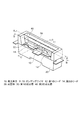
図1は、本発明の第1の実施形態にかかる発光装置の模式斜視図である。
図1に表す発光装置は、側面発光(サイドビュー)型とするが本発明はこれに限定されず、上面発光型であってもよい。発光素子10のチップ近傍を説明するために、図1は、第1の封止層30及び第2の封止層40をA−A線に沿って切断し、成型体20をB−B線に沿って切断した斜視図である。
Hereinafter, embodiments of the present invention will be described with reference to the drawings.
FIG. 1 is a schematic perspective view of a light emitting device according to a first embodiment of the present invention.
The light emitting device shown in FIG. 1 is a side emission type, but the present invention is not limited to this and may be a top emission type. In order to describe the vicinity of the chip of the
第1のリード12を、例えばカソード電極とすると、第2のリード14はアノード電極である。第1及び第2のリード12、14は熱可塑性樹脂などからなる成型体20に埋め込まれているが、それぞれのインナーリード部は成型体20の内部で対向しており、アウターリード部は反対方向に向かって成型体20から突出している。なお、成型体20は凹部20aを有しており、凹部20aの底面には第1のリード12が露出し発光素子10が銀ペーストなどを用いて接着されている。また、発光素子10は、ボンディングワイヤ11により第1のリード12と、ボンディングワイヤ19により第2のリード14と、それぞれ接続されている。
When the
発光素子10は、第1の透光性樹脂(屈折率n1は略1.5)に第1の蛍光体の所要重量が混合された第1の混合樹脂からなる第1の封止層30により覆われている。発光素子10から放出された1次光の一部は、第1の透光性樹脂に混合された蛍光体に吸収され、波長が異なる波長変換光に変換される。第1の封止層30は、蛍光体粒子が混合されていない第2の透光性樹脂(屈折率n2は略1.4)からなる第2の封止層40により覆われている。第1の透光性樹脂及び第2の透光性樹脂を、例えばシリコーン系樹脂とすると、発光素子10から放出される1次光による樹脂の変色を抑制できる。
The light-emitting
また、発光素子10を窒化物系半導体とすると、発光素子10から放出される1次光としての青色光と、珪酸塩系材料からなる黄色蛍光体による波長変換光と、の混合光として白色光などを得ることができ、表示装置のバックライト光源として用いることができる。
Further, when the
図2は、第1の実施形態にかかる発光装置の製造方法を説明するフロー図である。
発光素子10から放出される1次光の波長λd及び光出力Poなどはウェーハの面内において分布している。これらの特性の分布許容範囲を狭くしすぎると、良品チップの収量が減少する。他方、分布許容範囲を広くしすぎると、発光装置の色度変動が大きくなり光学特性の品位が低下する。
FIG. 2 is a flowchart illustrating the method for manufacturing the light emitting device according to the first embodiment.
The wavelength λd of the primary light emitted from the
まず予備工程として、1次光のウェーハ内の波長λd及び光出力Poの分布を測定し(S100)、適正な分布許容範囲を、例えば、15≦Po(mW)≦17、及び450≦λd(nm)≦460などと設定する。 First, as a preliminary process, the distribution of the wavelength λd and the light output Po in the wafer of the primary light is measured (S100), and appropriate distribution allowable ranges are, for example, 15 ≦ Po (mW) ≦ 17 and 450 ≦ λd ( nm) ≦ 460 or the like.
続いて、設定された波長λd及び光出力Poの分布許容範囲内にある発光素子10を抜き取り、これを用いた発光装置を組み立てる。これらの発光装置は、放出する混合光の色度が例えば0.294≦Cx≦0.304とされる所定の色度範囲を有するものを含むように準備され、その混合光の色度が分光装置を有する光学特性測定装置60を用いて測定される。このようにして、混合光の色度の1次光の波長に対する依存性(波長依存性)及び1次光の光出力に対する依存性(光出力依存性)を求める(S101)。
Subsequently, the
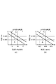
図3は、混合光の色度Cxを表すグラフ図である。すなわち、図3(a)は発光装置から放出される混合光の色度Cxの、1次光の光出力に対する依存性、図3(b)は混合光の色度Cxの、1次光の波長に対する依存性、をそれぞれ表す。縦軸は色度図の色度座標Cxであり、横軸は発光素子から放出される1次光の光出力Po(mW)または波長λd(nm)である。 FIG. 3 is a graph showing the chromaticity Cx of the mixed light. 3A shows the dependence of the chromaticity Cx of the mixed light emitted from the light emitting device on the light output of the primary light, and FIG. 3B shows the dependency of the primary light on the chromaticity Cx of the mixed light. Dependence on wavelength is expressed respectively. The vertical axis represents the chromaticity coordinates Cx of the chromaticity diagram, and the horizontal axis represents the light output Po (mW) or wavelength λd (nm) of the primary light emitted from the light emitting element.
図3(a)は、1次光の波長λdを分布上限値である460nmに保ちつつ、蛍光体配合比ai(i=1、・・・、N、N:整数)をパラメータとして混合樹脂液を同一容積充填した場合の混合光の色度Cxの1次光の光出力に対する依存性を近似的に表している。なお、蛍光体配合比aiは、混合樹脂液重量に対する蛍光体重量の割合であり、重量(wt)%で表すことにする。蛍光体配合比aiは、例えば5〜50wt%などの範囲とすることができる。 FIG. 3 (a) shows the mixed resin with the phosphor blending ratio a i (i = 1,..., N, N: integer) as parameters while keeping the wavelength λd of the primary light at the distribution upper limit value of 460 nm. The dependence of the chromaticity Cx of the mixed light on the light output of the primary light when the liquid is filled in the same volume is approximately expressed. The phosphor blending ratio a i is the ratio of the phosphor weight to the mixed resin liquid weight, and is expressed by weight (wt)%. Phosphor compounding ratio a i may be, for example, a range such as 5-50 wt%.
蛍光体配合比aiを一定とする場合、1次光の光出力Poが低くなると混合光の色度Cxが大きくなる。また、蛍光体配合比aiを小さくすると、波長変換光である黄色光の強度が低下し混合光の色度Cxが小さくなり、1次光の青色光に近づく。一般に、混合光の色度Cxの、1次光の光出力に対する依存性は、直線で表せるとは限らない。しかしながら、1次光の光出力Poの分布許容範囲をその中心値のプラスマイナス10%以下の狭い範囲とすると混合光の色度Cxを直線近似することが可能となり、蛍光体重量の算出方法が簡素となる。また、直線近似することにより、予備工程で組み立てる発光装置の数を低減できる。なお、波長λdを許容分布範囲上限値の460nmよりも短い一定波長値とした光出力依存性も求めておく。 When the phosphor blending ratio a i is constant, the chromaticity Cx of the mixed light increases as the light output Po of the primary light decreases. Further, when the phosphor blending ratio a i is reduced, the intensity of yellow light, which is wavelength converted light, is reduced, the chromaticity Cx of the mixed light is reduced, and it approaches blue light of primary light. In general, the dependency of the chromaticity Cx of the mixed light on the light output of the primary light is not always expressed by a straight line. However, if the distribution allowable range of the light output Po of the primary light is a narrow range of plus or minus 10% or less of the central value, the chromaticity Cx of the mixed light can be linearly approximated, and the phosphor weight calculation method is It becomes simple. Moreover, the number of light emitting devices assembled in the preliminary process can be reduced by linear approximation. The light output dependency is also determined in which the wavelength λd is a constant wavelength value shorter than the allowable distribution range upper limit value of 460 nm.
他方、図3(b)は、1次光の光出力Poを分布上限値である17mWに保ちつつ、蛍光体配合比aiをパラメータとして第1の混合樹脂液を同一容積充填した場合の混合光の色度Cxの波長依存性を近似的に表している。蛍光体配合比aiを一定とする場合、1次光の波長が短くなると混合光の色度Cxが大きくなる。また、蛍光体配合比aiを小さくすると、波長変換光である黄色光の強度が低下し混合色の色度Cxが小さくなる。一般に、混合光の色度Cxの、1次光の波長に対する依存性も直線で表せるとは限らない。しかしながら、波長λdの分布許容範囲をその中心値のプラスマイナス1.5%以下の狭い範囲とすると直線近似が可能であり、蛍光体重量の算出方法が簡素となる。なお、1次光の光出力Poを許容分布範囲上限値の17mWよりも低い一定値とした波長依存性も求めておく。 On the other hand, FIG. 3B shows the mixing in the case where the same volume of the first mixed resin liquid is filled using the phosphor blending ratio a i as a parameter while keeping the light output Po of the primary light at the distribution upper limit value of 17 mW. This schematically represents the wavelength dependence of the chromaticity Cx of light. When the phosphor blending ratio a i is constant, the chromaticity Cx of the mixed light increases as the wavelength of the primary light decreases. Further, when the phosphor blending ratio a i is decreased, the intensity of yellow light that is wavelength converted light is decreased, and the chromaticity Cx of the mixed color is decreased. In general, the dependence of the chromaticity Cx of the mixed light on the wavelength of the primary light is not always expressed by a straight line. However, if the allowable distribution range of the wavelength λd is a narrow range of plus or minus 1.5% or less of the center value, linear approximation is possible, and the phosphor weight calculation method becomes simple. In addition, the wavelength dependency in which the light output Po of the primary light is a constant value lower than the allowable distribution range upper limit value of 17 mW is also obtained.
また、発光素子10のウェーハ製造プロセス条件を精度良く制御すると、図3に表す波長依存性及び光出力依存性がウェーハ毎に大きく変動することを抑制でき、これら依存性の導出は容易となる。
Further, if the wafer manufacturing process conditions of the
混合光の色度Cxの所定の範囲を、0.294〜0.304とする場合、例えばその目標値を0.3などとすることができる。1次光のPo=17mW(光出力上限値)且つλ=460nm(波長上限値)において、Cx=0.3とするような蛍光体配合比a1を図3などを用いて決定可能である(S102)。以上により予備工程を完了する。 When the predetermined range of the chromaticity Cx of the mixed light is 0.294 to 0.304, for example, the target value can be 0.3. When the primary light Po = 17 mW (light output upper limit value) and λ = 460 nm (wavelength upper limit value), it is possible to determine a phosphor blending ratio a1 such that Cx = 0.3 using FIG. S102). Thus, the preliminary process is completed.
次に、発光装置の組立工程を行う。 Next, an assembly process of the light emitting device is performed.
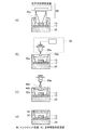
図4は、樹脂を封止する工程断面図であり、図1においてC−C線に沿った断面を表している。 FIG. 4 is a process cross-sectional view for sealing the resin, and represents a cross section taken along the line CC in FIG.
個々の発光素子10をパッケージに接着し、ワイヤボンディングを行う(S104)。続いて、図4(a)のように、個々の発光素子10の波長λd及び光出力Poを光学特性測定装置60を用いて測定する(S106)。
The individual
予備工程において求めておいた混合光の色度Cxの1次光の波長に対する依存性(図3(a))及び光出力に対する依存性(図3(b))と、個々の発光素子10の1次光の波長及び光出力の測定値と、に基づいて、蛍光体粒子の所要重量bを算出する工程を以下で説明する。
The dependency of the chromaticity Cx of the mixed light obtained in the preliminary process on the wavelength of the primary light (FIG. 3A) and the dependency on the light output (FIG. 3B), and the individual
図5は、蛍光体粒子の重量の算出方法を説明する図である。すなわち、図5(a)は、1次光の波長λdが上限値460nmの場合、波長変換光の色度Cxを目標値0.3とするための蛍光体配合比の光出力依存性を表すグラフ図、図5(b)は混合樹脂の最大容積を説明する図、図5(c)は混合樹脂と透光性樹脂との2層構造を表す模式断面図である。
FIG. 5 is a diagram for explaining a method of calculating the weight of the phosphor particles. That is, FIG. 5A shows the light output dependency of the phosphor mixture ratio for setting the chromaticity Cx of the wavelength-converted light to the target value 0.3 when the wavelength λd of the primary light is the
図5(a)において、縦軸は蛍光体配合比(wt%)、横軸は1次光の光出力Po(mW)、を表す。
予備工程において、図3(a)のように蛍光体配合比aiを表す曲線をN本求めておくことができる。これらの曲線群に基づいて1次光の光出力に対する依存性を直線近似した場合、図5のようになる。Po=17mW且つλd=460nmに対応する点Qでは、蛍光体粒子の重量が最大となるので、蛍光体配合比も最大値(a1)となる。
In FIG. 5A, the vertical axis represents the phosphor blending ratio (wt%), and the horizontal axis represents the light output Po (mW) of the primary light.
In the preliminary process, N curves representing the phosphor blending ratio a i can be obtained as shown in FIG. When the dependence on the light output of the primary light is linearly approximated based on these curve groups, the result is as shown in FIG. At the point Q corresponding to Po = 17 mW and λd = 460 nm, the weight of the phosphor particles is maximized, so that the phosphor blending ratio is also the maximum value (a 1 ).
S106の測定工程において、チップ(発光素子)から放出される1次光の光出力Poxが光出力上限値の17mWよりも低いものとする。なお、説明を簡単にするために1次光の波長λdは上限値460nmとする。蛍光体配合比の光出力依存性を用いて、光出力Poxに対応する蛍光体配合比axを読み取る。この場合、蛍光体粒子の重量bは式(1)より算出できる。 In S106 of the measurement process, the chip optical output Po x of the primary light emitted from the (light emitting element) and lower than 17mW optical output upper limit value. In order to simplify the description, the wavelength λd of the primary light is set to an upper limit value of 460 nm. Using the light output dependency of phosphor compounding ratio, it reads the phosphor compounding ratio a x corresponding to the light output Po x. In this case, the weight b of the phosphor particles can be calculated from the formula (1).
b=Vpm×rx×ax 式(1)
但し、Vpm:凹部(カップ)内の混合樹脂を充填可能な最大容積(チップ容積を除く)
rx:蛍光体配合比axの混合樹脂の密度
b = Vpm × r x × a x Formula (1)
However, Vpm: the maximum volume that can be filled with the mixed resin in the recess (cup) (excluding the chip volume)
r x : Density of mixed resin with phosphor blending ratio a x
第1の実施形態における実装工程では、蛍光体配合比をa1とし混合樹脂の容積を制御する。蛍光体配合比a1の混合樹脂の容積Vpは式(2)により算出できる。 The mounting process of the first embodiment, controls the volume of the mixed resin and a 1 phosphor compounding ratio. The volume Vp of the mixed resin having the phosphor blending ratio a 1 can be calculated by the equation (2).
Vp=b/(r1×a1 )
=Vpm×(rx×ax)/(r1×a1) 式(2)
但し、r1:蛍光体配合比a1の混合樹脂の密度
読み取られた蛍光体配合比axは蛍光体配合比a1(最大値)よりも小さく、且つrxはr1よりも小さいので、混合樹脂の容積Vpは最大容積Vpm以下となる(S108)。すなわち、個々の発光装置ごとに、混合光の色度Cxが所定の範囲内となるように、混合樹脂の容積Vpが制御される。
Vp = b / (r 1 × a 1 )
= Vpm × (r x × a x) / (r 1 × a 1) (2)
However, r 1 : Density of mixed resin of phosphor blending ratio a 1
Since the read phosphor blending ratio a x is smaller than the phosphor blending ratio a 1 (maximum value) and r x is smaller than r 1 , the volume Vp of the mixed resin is not more than the maximum volume Vpm (S108). . That is, the volume Vp of the mixed resin is controlled so that the chromaticity Cx of the mixed light is within a predetermined range for each light emitting device.
なお、図5は、1次光の波長λdがその上限値である460nmと一定の場合について説明したが本発明はこれに限定されない。1次光の光出力をその上限値17mWと一定とし、波長が変化した場合には、図3(b)をもとに、蛍光体配合比の波長依存性を求めることができる。このあと、式(2)を用いて蛍光体粒子の所要重量b及び混合樹脂容積を算出することができる。
また、図3(a)では1次光の波長λdが分布許容範囲の上限値である460nmとし、図3(b)では1次光の光出力Poが分布許容範囲の上限値である17mWとしている。1次光の波長λdが460nmよりも短く、且つ光出力Poが17mWよりも低い範囲にある場合、同一の蛍光体配合比では混合光の色度Cxがより高くなるので、光出力依存性及び波長依存性を表す曲線群は図3よりも全体的に上方へシフトする。これらの曲線群は、予備工程のS101で求めておくことができる。
この場合、同一色度とするための蛍光体配合比は、図5に表す曲線よりも下方へシフトした曲線を用いて求めることができる。
In addition, although FIG. 5 demonstrated the case where wavelength (lambda) d of primary light was constant with 460 nm which is the upper limit, this invention is not limited to this. When the light output of the primary light is constant at its upper limit value of 17 mW and the wavelength changes, the wavelength dependency of the phosphor blending ratio can be obtained based on FIG. Thereafter, the required weight b of the phosphor particles and the mixed resin volume can be calculated using the equation (2).
Further, in FIG. 3A, the wavelength λd of the primary light is set to 460 nm which is the upper limit value of the allowable distribution range, and in FIG. 3B, the light output Po of the primary light is set to 17 mW which is the upper limit value of the allowable distribution range. Yes. When the wavelength λd of the primary light is shorter than 460 nm and the light output Po is in a range lower than 17 mW, the chromaticity Cx of the mixed light becomes higher with the same phosphor blending ratio. The group of curves representing the wavelength dependence is shifted upward as a whole from FIG. These curve groups can be obtained in S101 of the preliminary process.
In this case, the phosphor blending ratio for achieving the same chromaticity can be obtained using a curve shifted downward from the curve shown in FIG.
続いて、図4(b)のように、蛍光体配合比a1とした混合樹脂液30aを容積Vpに相当する量だけインクジェット装置のノズル50aから吐出し凹部20a内に滴下する(S110)。または、ディスペンサを用いて滴下を行ってもよい。
Subsequently, as shown in FIG. 4 (b), it dropped into the
さらに、図4(c)のように、他のノズルを用いて蛍光体粒子が含まれない第2の透光性樹脂液40a(屈折率n2、n2≦n1)を容積Vt(=Vc−Vp)に相当する量だけ滴下する。第2の透光性樹脂40bからなる第2の封止層40を設けると、第1の封止層30の容積Vpの変化による放出光の指向特性の変動を抑制することが容易となる。なお、Vcは成型体20の凹部20a(カップ)容積を表すものとする。
Further, as shown in FIG. 4C, the second translucent resin liquid 40a (refractive index n2, n2 ≦ n1) containing no phosphor particles is added to the volume Vt (= Vc−Vp) using another nozzle. ) Is dripped in an amount corresponding to). Providing the
続いて、例えば150℃で略2時間の熱処理による樹脂硬化工程を行い(S112)、図4(d)のように第1の封止層30、第2の透光性樹脂40bからなる第2の封止層40が凹部20a内に積層された発光装置が完成する。すなわち、図5(c)のように、蛍光体粒子30cが分散配置された第1の封止層30と、蛍光体粒子が分散配置されない第2の封止層40と、の2層構造とすることができる。
なお、蛍光体配合比aiが異なるノズルに切り替えるか、または複数のノズルを用いることにより蛍光体重量bを制御することも可能である。この場合、発光素子10の波長λd及び光出力Poが変動しても、混合樹脂液30aの容積を、略最大容積Vpmとすることが容易となる。
Subsequently, for example, a resin curing process is performed by heat treatment at 150 ° C. for about 2 hours (S112), and a
Note that the phosphor weight b can be controlled by switching to a nozzle having a different phosphor blending ratio a i or by using a plurality of nozzles. In this case, even if the wavelength λd and the light output Po of the
図6は、混合光の色度Cxの度数分布を表すグラフ図である。すなわち、図6(a)は本実施形態、図6(b)は比較例をそれぞれ表す。縦軸は度数、横軸は混合光の色度Cxである。
所定の色度範囲0.294〜0.304に対して、図6(a)に表す本実施形態において、混合光の色度Cxが0.296〜0.303の間に制御されている。他方、蛍光体重量を制御しない比較例において、混合光の色度Cxは、0.281〜0.312の間に広く分布し、所定の範囲内に保つことが困難である。すなわち、比較例では色度変動が大きく、混合光の光学特性の品位が不十分となるのに対して、本実施形態では色度の制御が容易であり、光学特性の品位が高められた発光装置及び良品率が改善された発光装置の製造方法が提供される。
FIG. 6 is a graph showing the frequency distribution of the chromaticity Cx of the mixed light. 6A shows this embodiment, and FIG. 6B shows a comparative example. The vertical axis represents the frequency, and the horizontal axis represents the chromaticity Cx of the mixed light.
In this embodiment shown in FIG. 6A for a predetermined chromaticity range of 0.294 to 0.304, the chromaticity Cx of the mixed light is controlled between 0.296 and 0.303. On the other hand, in the comparative example in which the phosphor weight is not controlled, the chromaticity Cx of the mixed light is widely distributed between 0.281 to 0.312 and is difficult to keep within a predetermined range. That is, the chromaticity variation is large in the comparative example and the quality of the optical characteristics of the mixed light becomes insufficient, whereas in this embodiment, the chromaticity is easily controlled, and the light emission with improved quality of the optical characteristics. A device and a method for manufacturing a light emitting device with improved yield rate are provided.
なお、図2には、1次光の波長と光出力を測定し、また1次光の波長と光出力に対する混合光の色度の依存性をそれぞれ測定する具体例を表したが、本発明はこれには限定されない。 FIG. 2 shows a specific example in which the wavelength and light output of the primary light are measured, and the dependency of the chromaticity of the mixed light on the wavelength and light output of the primary light is measured. Is not limited to this.
例えば、1次光の波長のバラツキが比較的小さい場合には、1次光の光出力のみを測定し、また1次光の光出力に対する混合光の色度の依存性を測定して、蛍光体粒子の所要量を求めてもよい。一方、これとは逆に、1次光の光出力のバラツキが比較的小さい場合には、1次光の波長のみを測定し、また1次光の波長に対する混合光の色度の依存性を測定して、蛍光体粒子の所要量を求めてもよい。 For example, when the variation in the wavelength of the primary light is relatively small, only the light output of the primary light is measured, and the dependence of the chromaticity of the mixed light on the light output of the primary light is measured to obtain fluorescence. The required amount of body particles may be determined. On the other hand, when the variation in the light output of the primary light is relatively small, only the wavelength of the primary light is measured, and the dependency of the chromaticity of the mixed light on the wavelength of the primary light is measured. The required amount of phosphor particles may be determined by measurement.
図7は、第2の実施形態にかかる発光装置を説明する色度図である。
本実施形態にかかる発光装置は、発光素子10から放出され波長が450〜460nmの範囲である青色光である1次光Bと、窒化物系材料やYAG(Yttrium-Aluminum-Garnet)などからなる緑色蛍光体からの波長変換光Gと、窒化物系材料やYAGなどからなる赤色蛍光体からの波長変換光Rと、が混合された混合光Wを放出可能とする。
FIG. 7 is a chromaticity diagram illustrating the light emitting device according to the second embodiment.
The light emitting device according to the present embodiment includes primary light B that is blue light emitted from the
この場合にもウェーハ内で分布している青色の1次光Bの波長λd及び光出力Poを測定し(図2のS100)、その分布許容範囲を設定する。 Also in this case, the wavelength λd of the blue primary light B distributed in the wafer and the optical output Po are measured (S100 in FIG. 2), and the allowable distribution range is set.
設定された波長λd及び光出力Poの分布許容範囲内の発光素子10を抜き取り、これを用いた発光装置を組み立てる。この場合、混合光Wの色度が所定の範囲内となるような、緑色蛍光体と赤色蛍光体との適正な混合比を設定する。この混合比を保ちつつ、第1の混合樹脂液30aに対するそれぞれの蛍光体配合比を変化して混合光Wの色度(Cx、Cy)を測定し、混合光の色度の波長依存性及び光出力依存性などを求める(S101)。
The
これらの依存性を用いて、分布許容範囲の上限となる1次光のPo=17mW且つλ=460nmにおいて、色度目標値とできるような緑色蛍光体配合比(最大値)及び赤色蛍光体配合比(最大値)をそれぞれ決定する(S102)。以上により、予備工程が終了する。 Using these dependencies, the green phosphor blending ratio (maximum value) and red phosphor blending that can be set as the chromaticity target value at Po = 17 mW and λ = 460 nm of the primary light that is the upper limit of the allowable distribution range Each ratio (maximum value) is determined (S102). Thus, the preliminary process is completed.
次に、発光装置の組立工程を行う。個々の発光素子10をパッケージに接着し、ワイヤボンディングを行う(S104)。続いて、個々の発光素子10の1次光の波長λd及び光出力Poを分光装置などの光学特性測定装置60を用いて測定する(S106)。
Next, an assembly process of the light emitting device is performed. The individual
予備工程において求めておいた混合光の色度の1次光の波長に対する依存性及び光出力に対する依存性と、1次光の波長λd及び光出力Poの測定値と、に基づいて、緑色蛍光体粒子及び赤色蛍光体粒子の所要重量をそれぞれ算出する(S108)。
所要重量の蛍光体粒子が混合された混合樹脂液をノズルから滴下し(S110)、混合樹脂液を硬化し(S112)、組立工程を終了する。
Based on the dependence of the chromaticity of the mixed light on the wavelength of the primary light and the dependence on the light output obtained in the preliminary process, and the measured values of the wavelength λd of the primary light and the light output Po, the green fluorescence The required weights of the body particles and the red phosphor particles are calculated (S108).
The mixed resin liquid mixed with the required weight of phosphor particles is dropped from the nozzle (S110), the mixed resin liquid is cured (S112), and the assembly process is completed.
図8は、第2の実施形態の模式断面図である。すなわち、図8(a)は2つの蛍光体粒子が共通の透光性樹脂31bに分散配置された封止層31、図8(b)はそれぞれの蛍光体粒子が分散配置された2つの封止層32、33、を有する構造をそれぞれ表す。
FIG. 8 is a schematic cross-sectional view of the second embodiment. 8A shows a
第1の蛍光体粒子31cと第2の蛍光体粒子31dとの混合比は、あらかじめ設定できる。図8(a)では、インクジェット装置50に、蛍光体粒子31cと31dとの設定された混合比を有する混合樹脂液を準備し、発光素子10を覆うように所要容積を滴下し、熱硬化などにより第3の封止層31とする。蛍光体粒子31cを含む混合樹脂液と、蛍光体粒子31dを含む混合樹脂液と、をそれぞれ別に準備し、それぞれのノズルから滴下してもよい。また、第3の封止層31の上に、透光性樹脂からなる第2の封止層40をさらに設けてもよい。
The mixing ratio of the
図8(b)では、まず透光性樹脂32bに所要重量の蛍光体粒子32dが混合された混合樹脂液を準備し、発光素子10のチップ上に滴下する。さらに、透光性樹脂33bに所要重量の蛍光体粒子33cが混合された混合樹脂液を滴下する。このあと熱硬化により、第4及び第5の封止層32、33が形成される。なお、熱硬化により第4の封止層32を形成後、混合樹脂液をその上から滴下して第5の封止層33を形成してもよい。また、第5の封止層33の上に、透光性樹脂からなる第2の封止層40をさらに設けてもよい。このようにして、図7に表す色度図において、混合色Wを目標とする色度範囲に制御することが容易となる。
In FIG. 8B, first, a mixed resin liquid in which
第1及び第2の実施形態において、所定の色度範囲に制御された混合光を放出可能な発光装置、及びこれを用いた照明装置が可能となる。例えば、これらの発光装置を側面発光型として配列したバックライト光源を構成すると、色度が均一且つ高画質な表示装置が容易となる。 In the first and second embodiments, a light emitting device capable of emitting mixed light controlled in a predetermined chromaticity range and a lighting device using the light emitting device can be realized. For example, when a backlight light source in which these light emitting devices are arranged as a side light emitting type is configured, a display device with uniform chromaticity and high image quality is facilitated.
以上、図面を参照しつつ本発明の実施形態について説明した。しかしながら、本発明はこれらの実施形態に限定されない。発光装置を構成する透光性樹脂、蛍光体粒子、成型体、リード、及び発光素子、などの材料、サイズ、形状、配置などに関して、当業者が各種の設計変更を行ったものであっても、本発明の主旨を逸脱しない限り本発明の範囲に包含される。 The embodiments of the present invention have been described above with reference to the drawings. However, the present invention is not limited to these embodiments. Even if those skilled in the art have made various design changes with respect to materials, sizes, shapes, arrangements, etc., such as translucent resin, phosphor particles, molded bodies, leads, and light emitting elements constituting the light emitting device. It is included in the scope of the present invention without departing from the gist of the present invention.
10 発光素子、20 成型体、20a 凹部、30 第1の封止層、30a 第1の混合樹脂液、30b 第1の透光性樹脂、30c、31c(第1の)蛍光体粒子、31d 第2の蛍光体粒子、40 第2の封止層、40b 第2の透光性樹脂 50 インクジェット装置、50a ノズル、ai 蛍光体配合比、b 蛍光体所要重量
DESCRIPTION OF
Claims (5)
前記1次光の波長または前記1次光の光出力のうちの少なくとも一方に対する前記混合光の色度の依存性をあらかじめ求める工程と、
発光素子毎に前記1次光の波長または前記1次光の光出力のうちの少なくとも一方を測定する工程と、
前記求めた前記1次光の波長または前記1次光の光出力のうちの少なくとも一方に対する前記混合光の色度の依存性と、前記測定した前記1次光の波長または前記1次光の光出力のうちの少なくとも一方と、に基づいて前記混合光の色度を所定の範囲内とするための前記蛍光体粒子の所要量を求める工程と、
前記所要量の前記蛍光体粒子を混合した前記第1の透光性樹脂により、前記発光素子を覆う工程と、
を備えたことを特徴とする発光装置の製造方法。 A light-emitting element capable of emitting primary light; and a first translucent resin mixed with phosphor particles capable of absorbing the primary light and emitting wavelength-converted light. And a method of manufacturing a light emitting device that emits mixed light including the wavelength-converted light,
Obtaining in advance the dependence of the chromaticity of the mixed light on at least one of the wavelength of the primary light or the light output of the primary light;
Measuring at least one of the wavelength of the primary light or the light output of the primary light for each light emitting element;
Dependence of the chromaticity of the mixed light on at least one of the obtained wavelength of the primary light or the light output of the primary light, and the measured wavelength of the primary light or the light of the primary light Obtaining a required amount of the phosphor particles for setting the chromaticity of the mixed light within a predetermined range based on at least one of the outputs; and
Covering the light emitting element with the first translucent resin mixed with the required amount of the phosphor particles;
A method for manufacturing a light emitting device, comprising:
前記1次光の波長または前記1次光の光出力のうち少なくとも一方があらかじめ決めた許容される上限値の場合に求められる前記混合光の色度を前記所定の範囲内とするための前記蛍光体粒子の所要量と、前記凹部内を充填するための所定の容積とに基づいて、前記所定の容積中に前記所要量の前記蛍光体粒子が含まれる所定の配合比を有する前記第1の透光性樹脂をあらかじめ用意する工程と、
をさらに備え、
前記発光素子を覆う工程は、前記発光素子毎に求められた前記蛍光体粒子の所要量に応じて前記所定の配合比を有する前記第1の透光性樹脂を前記凹部内に必要量充填して覆う工程であることを特徴とする請求項1記載の発光装置の製造方法。 The first translucent resin covers the light emitting element in a recess,
The fluorescence for setting the chromaticity of the mixed light, which is obtained when at least one of the wavelength of the primary light or the light output of the primary light is a predetermined allowable upper limit value, within the predetermined range Based on a required amount of body particles and a predetermined volume for filling the recess, the first mixture having a predetermined mixing ratio in which the predetermined amount of the phosphor particles is included in the predetermined volume. A step of preparing a translucent resin in advance;
Further comprising
The step of covering the light emitting element includes filling the recess with a necessary amount of the first translucent resin having the predetermined blending ratio according to the required amount of the phosphor particles obtained for each light emitting element. The method of manufacturing a light emitting device according to claim 1, wherein the manufacturing method is a step of covering.
前記波長変換光は、前記第1の波長変換光と、前記第2の波長変換光と、を含むことを特徴とする請求項1〜3のいずれかに記載の発光装置の製造方法。 The phosphor particles are capable of absorbing the primary light and emitting a first wavelength converted light, and absorbing the primary light and a wavelength of the first wavelength converted light. Comprises second phosphor particles capable of emitting second wavelength-converted light having different wavelengths,
The method for manufacturing a light-emitting device according to claim 1, wherein the wavelength-converted light includes the first wavelength-converted light and the second wavelength-converted light.
Priority Applications (6)
| Application Number | Priority Date | Filing Date | Title |
|---|---|---|---|
| JP2008274254A JP2010103349A (en) | 2008-10-24 | 2008-10-24 | Method of manufacturing light emitting device |
| PCT/JP2009/000544 WO2009118985A2 (en) | 2008-03-25 | 2009-02-10 | Light emitting device, and method and apparatus for manufacturing same |
| KR1020107018221A KR101226777B1 (en) | 2008-03-25 | 2009-02-10 | Light emitting device, and method and apparatus for manufacturing same |
| EP09723886.9A EP2257999B1 (en) | 2008-03-25 | 2009-02-10 | Light emitting device, and method and apparatus for manufacturing same |
| US12/867,145 US8268644B2 (en) | 2008-03-25 | 2009-02-10 | Light emitting device, and method and apparatus for manufacturing same |
| TW098108070A TWI445202B (en) | 2008-03-25 | 2009-03-12 | A method for manufacturing a light emitting device |
Applications Claiming Priority (1)
| Application Number | Priority Date | Filing Date | Title |
|---|---|---|---|
| JP2008274254A JP2010103349A (en) | 2008-10-24 | 2008-10-24 | Method of manufacturing light emitting device |
Related Child Applications (1)
| Application Number | Title | Priority Date | Filing Date |
|---|---|---|---|
| JP2014006619A Division JP2014064046A (en) | 2014-01-17 | 2014-01-17 | Light-emitting device manufacturing method |
Publications (2)
| Publication Number | Publication Date |
|---|---|
| JP2010103349A true JP2010103349A (en) | 2010-05-06 |
| JP2010103349A5 JP2010103349A5 (en) | 2011-07-21 |
Family
ID=42293731
Family Applications (1)
| Application Number | Title | Priority Date | Filing Date |
|---|---|---|---|
| JP2008274254A Pending JP2010103349A (en) | 2008-03-25 | 2008-10-24 | Method of manufacturing light emitting device |
Country Status (1)
| Country | Link |
|---|---|
| JP (1) | JP2010103349A (en) |
Cited By (11)
| Publication number | Priority date | Publication date | Assignee | Title |
|---|---|---|---|---|
| WO2012032691A1 (en) * | 2010-09-09 | 2012-03-15 | パナソニック株式会社 | Led package manufacturing system |
| WO2012032692A1 (en) * | 2010-09-09 | 2012-03-15 | パナソニック株式会社 | Led-package manufacturing system |
| WO2012032694A1 (en) * | 2010-09-09 | 2012-03-15 | パナソニック株式会社 | Resin application device in led package manufacturing system |
| WO2012032693A1 (en) * | 2010-09-09 | 2012-03-15 | パナソニック株式会社 | Resin applying device of led package manufacturing system |
| WO2012036486A3 (en) * | 2010-09-15 | 2012-06-14 | (주)라이타이저코리아 | Light-emitting diode and method for producing same |
| JP2012174968A (en) * | 2011-02-23 | 2012-09-10 | Mitsubishi Electric Corp | Light-emitting device and light-emitting device group and manufacturing method |
| WO2013038611A1 (en) * | 2011-09-16 | 2013-03-21 | パナソニック株式会社 | System and method for manufacturing light emitting element, and system and method for manufacturing light emitting element package |
| WO2013051260A1 (en) * | 2011-10-06 | 2013-04-11 | パナソニック株式会社 | Resin coating device and resin coating method |
| WO2013129071A1 (en) * | 2012-02-27 | 2013-09-06 | シャープ株式会社 | Light-emitting device |
| JP2014003093A (en) * | 2012-06-15 | 2014-01-09 | Sharp Corp | Method for manufacturing light-emitting device and color measuring device |
| US9117980B2 (en) | 2012-01-27 | 2015-08-25 | Kabushiki Kaisha Toshiba | Light-emitting device including sealing units with different phosphor concentrations |
Citations (4)
| Publication number | Priority date | Publication date | Assignee | Title |
|---|---|---|---|---|
| JP2007053368A (en) * | 2005-08-12 | 2007-03-01 | Avago Technologies Ecbu Ip (Singapore) Pte Ltd | Phosphor conversion led device of improved uniformity in light distribution |
| JP2007066969A (en) * | 2005-08-29 | 2007-03-15 | Toshiba Lighting & Technology Corp | White light emitting diode and its fabrication process |
| US20070111344A1 (en) * | 2003-06-18 | 2007-05-17 | Tridonic Optoelectronics Gmbh | Method for the production of white leds and white led light source |
| JP2008091458A (en) * | 2006-09-29 | 2008-04-17 | Rohm Co Ltd | Method of evaluating illumination element |
-
2008
- 2008-10-24 JP JP2008274254A patent/JP2010103349A/en active Pending
Patent Citations (4)
| Publication number | Priority date | Publication date | Assignee | Title |
|---|---|---|---|---|
| US20070111344A1 (en) * | 2003-06-18 | 2007-05-17 | Tridonic Optoelectronics Gmbh | Method for the production of white leds and white led light source |
| JP2007053368A (en) * | 2005-08-12 | 2007-03-01 | Avago Technologies Ecbu Ip (Singapore) Pte Ltd | Phosphor conversion led device of improved uniformity in light distribution |
| JP2007066969A (en) * | 2005-08-29 | 2007-03-15 | Toshiba Lighting & Technology Corp | White light emitting diode and its fabrication process |
| JP2008091458A (en) * | 2006-09-29 | 2008-04-17 | Rohm Co Ltd | Method of evaluating illumination element |
Cited By (17)
| Publication number | Priority date | Publication date | Assignee | Title |
|---|---|---|---|---|
| CN102782890A (en) * | 2010-09-09 | 2012-11-14 | 松下电器产业株式会社 | Resin applying device of LED package manufacturing system |
| WO2012032692A1 (en) * | 2010-09-09 | 2012-03-15 | パナソニック株式会社 | Led-package manufacturing system |
| WO2012032694A1 (en) * | 2010-09-09 | 2012-03-15 | パナソニック株式会社 | Resin application device in led package manufacturing system |
| WO2012032693A1 (en) * | 2010-09-09 | 2012-03-15 | パナソニック株式会社 | Resin applying device of led package manufacturing system |
| JP2012059917A (en) * | 2010-09-09 | 2012-03-22 | Panasonic Corp | Resin coating apparatus in led package manufacturing system |
| JP2012059916A (en) * | 2010-09-09 | 2012-03-22 | Panasonic Corp | Led package manufacturing system |
| JP2012059915A (en) * | 2010-09-09 | 2012-03-22 | Panasonic Corp | Led package manufacturing system |
| JP2012059918A (en) * | 2010-09-09 | 2012-03-22 | Panasonic Corp | Resin coating apparatus in led package manufacturing system |
| WO2012032691A1 (en) * | 2010-09-09 | 2012-03-15 | パナソニック株式会社 | Led package manufacturing system |
| US9324906B2 (en) | 2010-09-09 | 2016-04-26 | Panasonic Intellectual Property Management Co., Ltd. | LED package manufacturing system |
| WO2012036486A3 (en) * | 2010-09-15 | 2012-06-14 | (주)라이타이저코리아 | Light-emitting diode and method for producing same |
| JP2012174968A (en) * | 2011-02-23 | 2012-09-10 | Mitsubishi Electric Corp | Light-emitting device and light-emitting device group and manufacturing method |
| WO2013038611A1 (en) * | 2011-09-16 | 2013-03-21 | パナソニック株式会社 | System and method for manufacturing light emitting element, and system and method for manufacturing light emitting element package |
| WO2013051260A1 (en) * | 2011-10-06 | 2013-04-11 | パナソニック株式会社 | Resin coating device and resin coating method |
| US9117980B2 (en) | 2012-01-27 | 2015-08-25 | Kabushiki Kaisha Toshiba | Light-emitting device including sealing units with different phosphor concentrations |
| WO2013129071A1 (en) * | 2012-02-27 | 2013-09-06 | シャープ株式会社 | Light-emitting device |
| JP2014003093A (en) * | 2012-06-15 | 2014-01-09 | Sharp Corp | Method for manufacturing light-emitting device and color measuring device |
Similar Documents
| Publication | Publication Date | Title |
|---|---|---|
| KR101226777B1 (en) | Light emitting device, and method and apparatus for manufacturing same | |
| JP2010103349A (en) | Method of manufacturing light emitting device | |
| US9287470B2 (en) | Wavelength-converting light emitting diode (LED) chip and LED device equipped with chip | |
| JP5025625B2 (en) | Method for manufacturing light emitting device | |
| JP2008288410A (en) | Semiconductor light-emitting device, and manufacturing method thereof | |
| KR20170123644A (en) | Light source assembly with improved color uniformity | |
| US8974852B2 (en) | Method of manufacturing light-emitting device with fluorescent layer | |
| KR20140005389U (en) | Double-chip light emitting diode | |
| CN105981187A (en) | Optoelectronic component | |
| KR101639143B1 (en) | Light-emitting module | |
| KR100585916B1 (en) | Light emitting diode | |
| JP5345414B2 (en) | Semiconductor light emitting device | |
| US9236414B2 (en) | Light-emitting device | |
| KR20170000512A (en) | Light emitting diode package | |
| KR100593161B1 (en) | White light emitting diode and manufacturing method thereof | |
| JP6743630B2 (en) | Light emitting device and manufacturing method thereof | |
| JP2008270390A (en) | Front cover, light-emitting device and manufacturing method for front cover | |
| JP2014064046A (en) | Light-emitting device manufacturing method | |
| JP4300980B2 (en) | Light emitting diode | |
| JP7232648B2 (en) | Light-emitting device and method for manufacturing light-emitting device | |
| KR20110108935A (en) | Light emitting apparatus and manufacturing method of the same | |
| CN109841721B (en) | Light emitting diode package and method of manufacturing the same | |
| KR20110121825A (en) | Semiconductor light emitting device package |
Legal Events
| Date | Code | Title | Description |
|---|---|---|---|
| A521 | Written amendment |
Free format text: JAPANESE INTERMEDIATE CODE: A523 Effective date: 20110601 |
|
| A621 | Written request for application examination |
Free format text: JAPANESE INTERMEDIATE CODE: A621 Effective date: 20110601 |
|
| A977 | Report on retrieval |
Free format text: JAPANESE INTERMEDIATE CODE: A971007 Effective date: 20130718 |
|
| A131 | Notification of reasons for refusal |
Free format text: JAPANESE INTERMEDIATE CODE: A131 Effective date: 20130723 |
|
| A521 | Written amendment |
Free format text: JAPANESE INTERMEDIATE CODE: A523 Effective date: 20130924 |
|
| A02 | Decision of refusal |
Free format text: JAPANESE INTERMEDIATE CODE: A02 Effective date: 20131017 |