JP2010091607A - Substrate for alignment - Google Patents
Substrate for alignment Download PDFInfo
- Publication number
- JP2010091607A JP2010091607A JP2008258537A JP2008258537A JP2010091607A JP 2010091607 A JP2010091607 A JP 2010091607A JP 2008258537 A JP2008258537 A JP 2008258537A JP 2008258537 A JP2008258537 A JP 2008258537A JP 2010091607 A JP2010091607 A JP 2010091607A
- Authority
- JP
- Japan
- Prior art keywords
- alignment
- colored layer
- substrate
- alignment mark
- mark
- Prior art date
- Legal status (The legal status is an assumption and is not a legal conclusion. Google has not performed a legal analysis and makes no representation as to the accuracy of the status listed.)
- Granted
Links
Images


Abstract
Description
本発明は、透明基板の一面に、アライメント用のアライメントマーク部を備えたアライメント用の基板に関し、特に、液晶表示パネル用のカラーフィルタ形成基板を作製するための基板に関する。 The present invention relates to an alignment substrate having an alignment mark portion for alignment on one surface of a transparent substrate, and more particularly to a substrate for producing a color filter forming substrate for a liquid crystal display panel.
近年、情報化社会への進展が著しく、ディスプレイ装置の使用も多様化し、種々のディスプレイ装置が開発、実用化されている。
特に、液晶表示装置は、CRT(Cathode−Ray Tube、ブラウン管) に代わり、広く普及されるようになってきた。
液晶表示装置用のカラー表示用の液晶パネルは、簡単には、TFT基板(TFT;Thin Film Transistor)とカラーフィルタ形成基板(対向基板とも言う)とを対向させ、両基板間に液晶を密封し、更に、TFT基板とカラーフィルタ形成基板の外側に、それぞれ、偏向板を配し、TFT基板の外側にバックライト部を配した構造で、バックライト部からの光が各色の着色層からなるカラーフィルタ(以下、CFとも言う)を通過して表示されるが、各色の着色層からなるカラーフィルタを通過する光は、画素毎に液晶をスイッチング素子としてオン−オフ制御されている。
液晶を制御する方式としては、各基板に垂直な縦方向の電界によって、液晶の配向方向を基板に直交する面内で回転させる方式(垂直電界方式とも言う)と、基板に平行な横方向の電界によって、基板に平行な面内で回転させる方式(横電界方式とも言う)とがある。
垂直電界方式の代表例がTN方式(Twisted Nematic mode)であり、横電界方式はIPS(In−Plane Switching)方式として知られている。
このような電界の制御は、通常、TN方式等の場合は、両基板にそれぞれ配設された透明導電膜(通常は、ITO膜〜錫をドープしたインジウム酸化物)からなる制御用の電極により行い、IPS方式(横電界方式)の場合は、TFT基板に配設された透明導電膜(ITO膜)の制御用の電極により行う。
最近では、垂直電界方式においては、良好に視野角を制御するために、カラーフィルタ形成基板に液晶配向機能突起が設けられるようになった。
In recent years, progress toward an information society has been remarkable, and the use of display devices has been diversified, and various display devices have been developed and put into practical use.
In particular, liquid crystal display devices have been widely used in place of CRT (Cathode-Ray Tube, CRT).
In a liquid crystal panel for color display for a liquid crystal display device, a TFT substrate (TFT; Thin Film Transistor) and a color filter forming substrate (also referred to as a counter substrate) are opposed to each other, and the liquid crystal is sealed between the substrates. In addition, a structure in which a deflection plate is arranged outside the TFT substrate and the color filter forming substrate and a backlight part is arranged outside the TFT substrate, and the light from the backlight part is a color layer composed of colored layers of each color. Light that passes through a filter (hereinafter also referred to as CF) is displayed, but light that passes through a color filter formed of a colored layer of each color is on-off controlled for each pixel using a liquid crystal as a switching element.
As a method of controlling the liquid crystal, a method in which the alignment direction of the liquid crystal is rotated in a plane perpendicular to the substrate by a vertical electric field perpendicular to each substrate (also referred to as a vertical electric field method), and a lateral direction parallel to the substrate are used. There is a method of rotating in a plane parallel to the substrate by an electric field (also referred to as a transverse electric field method).
A typical example of the vertical electric field method is a TN method (Twisted Nematic mode), and the horizontal electric field method is known as an IPS (In-Plane Switching) method.
Usually, in the case of the TN system or the like, such an electric field is controlled by a control electrode made of a transparent conductive film (usually ITO film to tin-doped indium oxide) disposed on both substrates. In the case of the IPS method (lateral electric field method), the control electrode of the transparent conductive film (ITO film) disposed on the TFT substrate is used.
Recently, in the vertical electric field method, in order to control the viewing angle well, a liquid crystal alignment function protrusion has been provided on the color filter forming substrate.
そして、従来から、TFT回路の形成用あるいはカラーフィルタ形成用のマスクとしては、透明基板の一面に転写時の露光光を実質的に遮光する遮光膜からなる、複数の図形パターンにて絵柄部全体を形成しているバイナリーマスクが用いられていたが、最近では、液晶表示パネルの作製の工程短縮を図るために、透明基板の一面に転写時の露光光を遮光する遮光膜と、前記露光光に対して半透過性のハーフトーン膜とを、それぞれパターニングして配し、遮光膜が配設された遮光領域と、遮光膜はなくハーフトーン膜が配設されたハーフトーン領域と、遮光膜とハーフトーン膜のいずれもが存在しない透明領域とを、設けた階調マスク(特開2007−188069号公報参照)や、解像限界以下の微細なスリットを配置して、露光量を調整する微細なスリットを有するスリットマスク(特開2002−196474号公報参照)の使用が行われるようになってきた。
例えば、階調マスクを用いて一括露光することにより、液晶表示装置用のカラーフィルタ形成基板における、液晶パネルの液晶を保持する間隔を制御するための柱状スペーサ(単に柱とも言う)および液晶配向機能突起を、着色層からなるカラーフィルタ形成の工程と同時に形成することが可能となる。(特開2005−84366号公報参照)
尚、階調マスクを作製するためには、例えば、透明基板上に半透明膜と遮光膜とが積層された専用のマスクブランクを使用し、マスクパターン製版を行えば良く、階調マスクは、スリットマスクのように微細なスリットを配置する必要がない点で有利である。
このような、階調マスクでは、透過率の異なる領域によって透過光の量を制御することにより、現像後のレジストの膜厚を2段階に制御することができる。
For example, a columnar spacer (also referred to simply as a column) and a liquid crystal alignment function for controlling the interval for holding the liquid crystal of a liquid crystal panel in a color filter forming substrate for a liquid crystal display device by performing batch exposure using a gradation mask The protrusions can be formed simultaneously with the process of forming a color filter composed of a colored layer. (See JP 2005-84366 A)
In order to fabricate a gradation mask, for example, a dedicated mask blank in which a translucent film and a light shielding film are laminated on a transparent substrate may be used, and mask pattern plate-making may be performed. This is advantageous in that it is not necessary to arrange fine slits unlike a slit mask.
In such a gradation mask, the resist film thickness after development can be controlled in two stages by controlling the amount of transmitted light according to regions having different transmittances.
上記のように、最近では、液晶表示パネルの作製の工程短縮を図り、柱状スペーサを、あるいは、柱状スペーサと液晶配向機能突起とを、着色層からなるカラーフィルタ形成の工程と同時に形成することが行われるようになってきた。
しかし、通常、1層目の着色層でアライメントマークを形成し、該マークに合わせて2層目以降の着色層を形成することとなるが、2層目以降の着色層を形成するための樹脂着色層1層が、1層目の着色層からなるアライメントマーク上を覆う状態となるが、この状態での1層目の着色層からなるアライメントマークの認識は、現状のプロキシミティー露光機ではできない。
例えば、層構成が、透明基板側から順に、樹脂BM〜R、G、Bの着色層〜ITO膜〜柱からなるTN方式のカラーフィルタ形成基板において、工程短縮のため、柱をR、G、Bの着色層の積層して形成する場合で、且つ、R、G、Bの着色層を、それぞれ、1層目の着色層、2層目の着色層、3層目の着色層としてこの順に形成する場合、アライメントマークが1層目の着色層(Rの着色層)で形成されるため、2層目以降のG、Bの着色層形成の工程、BM形成の工程におけるアライメント部は、2層目以降の着色層を形成するための樹脂着色層1層が、Rの着色層からなるアライメントマーク上を覆う状態となるが、現状のプロキシミティー露光機では、Rの着色層からなるアライメントマークを認識することができない。
このため、1層目の着色層で形成されるアライメントマークを露出するようにして、2層目以降の着色層を形成してアライメントを行っていた。(特願2008−008024参照)
また、1層目の着色層上にITO膜が塗布された状態として、BM膜を形成して、アライメントを行っていた。(特願2008−011848参照)
これらのアライメントの際、例えば、リング照明によりアライメントマーク部を照明して、CCDエリアセンサを撮像素子として撮像手段にて撮影していた。
However, usually, the alignment mark is formed by the first colored layer, and the second and subsequent colored layers are formed in accordance with the mark, but the resin for forming the second and subsequent colored layers One colored layer covers the alignment mark made up of the first colored layer, but the alignment mark made up of the first colored layer in this state cannot be recognized by the current proximity exposure machine. .
For example, in a TN type color filter forming substrate composed of colored layers of resin BM to R, G, and B, an ITO film, and columns in order from the transparent substrate side, the columns are formed of R, G, In the case of forming by laminating the colored layers of B, the colored layers of R, G, and B are formed in this order as a first colored layer, a second colored layer, and a third colored layer, respectively. When forming, since the alignment mark is formed by the first colored layer (R colored layer), the alignment portion in the second and subsequent G and B colored layer forming steps and the BM forming step is 2 The resin colored
For this reason, alignment is performed by forming the second and subsequent colored layers so that the alignment mark formed by the first colored layer is exposed. (See Japanese Patent Application No. 2008-008024)
In addition, alignment was performed by forming a BM film in a state where the ITO film was applied on the first colored layer. (See Japanese Patent Application No. 2008-011848)
At the time of these alignments, for example, the alignment mark portion is illuminated by ring illumination, and the CCD area sensor is used as an image sensor and the image is taken by the imaging means.
上記のように、最近では、液晶表示パネルの作製の工程短縮を図り、柱状スペーサを、あるいは、柱状スペーサと液晶配向機能突起とを、着色層からなるカラーフィルタ形成の工程と同時に形成することが行われるようになってきた。
そして、その際、1層目の着色層で形成されるアライメントマークが露出するようにして、2層目以降の着色層を形成してアライメントを行う、または、1層目の着色層上にITO膜が塗布された状態として、BM膜を形成してアライメントを行う、アライメント方法が採られていたが、1層目の着色層で形成されるアライメントマークを露出するようにしたり、1層目の着色層で形成されるアライメントマークを見易くするための工程が必要で、手間がかかり生産性の面や歩留まりの面で、その対応が求められていた。
本発明はこれに対応するもので、柱状スペーサを、あるいは、柱状スペーサと液晶配向機能突起とを、着色層からなるカラーフィルタ形成の工程と同時に形成するカラーフィルタ形成基板の作製方法において、1層目の着色層で形成されるアライメントマークを露出するようにしたり、1層目の着色層で形成されるアライメントマークを見易くするための工程を必要としないで、1層目の着色層で形成されるアライメントマークの位置を検出できる、アライメントマーク部の位置検出方法を可能とするアライメント用の基板を、提供しようとするものです。
As described above, recently, the process of manufacturing a liquid crystal display panel has been shortened, and columnar spacers, or columnar spacers and liquid crystal alignment function protrusions can be formed simultaneously with the process of forming a color filter composed of a colored layer. Has come to be done.
At that time, alignment is performed by forming the second and subsequent colored layers so that the alignment mark formed by the first colored layer is exposed, or ITO is formed on the first colored layer. In the state where the film is applied, the alignment method is performed in which the alignment is performed by forming the BM film. However, the alignment mark formed by the first colored layer is exposed or the first layer is exposed. A process for making the alignment mark formed of the colored layer easy to see is necessary, which is time-consuming and demanded in terms of productivity and yield.
The present invention is corresponding to this, and in the method for producing a color filter forming substrate, a columnar spacer or a columnar spacer and a liquid crystal alignment function protrusion are formed simultaneously with the step of forming a color filter comprising a colored layer. It is formed with the first colored layer without exposing the alignment mark formed with the colored layer of the eye or making the alignment mark formed with the first colored layer easy to see. It is intended to provide an alignment substrate that can detect the position of the alignment mark to be detected and enables a method for detecting the position of the alignment mark.
本発明のアライメント用の基板は、透明基板の一面に、アライメント用のアライメントマーク部を備えたアライメント用の基板であって、前記アライメントマーク部は、前記透明基板の一面に配設された着色層からなるマークと、該マーク領域全体を覆い、該マークの形状に沿い盛り上がるように配設された着色樹脂層1層とを備えていることを特徴とするものである。
そして、上記のアライメント用の基板であって、前記アライメントマーク部の、前記着色層からなるマークの幅を横切る断面のテーパー部(エッジ部とも言う)の平均傾きをθとした場合、tanθの値が0.028以上であることを特徴とするものである。
そして、上記いずれかのアライメント用の基板であって、カラーフィルタ形成基板作製用の基板であり、前記アライメントマーク部は、カラーフィルタ形成基板の作製における着色層のパターニングの際に用いられるものであることを特徴とするものであり、該前記カラーフィルタ形成基板は、透明基板の一面に、各色の着色層からなる各色のカラーフィルタ部、着色層からなるブラックマトリクス部(BM部とも言う)を有し、柱部(スペーサとも言う)を、各カラーフィルタ部やブラックマトリクス部を形成するための着色層で形成し、且つ、各色のカラーフィルタ部上にITO層を配している、液晶表示パネル用のカラーフィルタ形成基板であることを特徴とするものである。
尚、ここでは、アライメントマーク部の、着色層からなるマークの幅を横切る断面は、図3(a)に示すように、マークの形状に沿い盛り上がった部分の頂部22aは平坦状で、底側の面部22cは平坦状で、頂部22aの端から面部22cに到るテーパー部(エッジ部とも言う)22bは傾きをもち形成されていることを前提としている。
そして、ここでは、平均傾きは、概略的に、アライメントマーク部の断面の表面形状が、図3(d)の示すような場合、テーパー部(エッジ部)22bの底の勾配が緩やかな立ち上がり部、頂点付近の勾配が緩やかな部分を除いた領域の平均勾配としている。
また、ここでのアライメントマーク部は、その領域を正反射照明(落射照明)にて撮影した画像から、画像処理により、該アライメントマーク部の位置を検出するためのものであることを前提としている。
The alignment substrate of the present invention is an alignment substrate provided with an alignment mark portion for alignment on one surface of a transparent substrate, and the alignment mark portion is a colored layer disposed on one surface of the transparent substrate. And a colored resin layer that covers the entire mark region and is arranged so as to rise along the shape of the mark.
When the average inclination of the taper portion (also referred to as an edge portion) of the cross section across the width of the mark made of the colored layer in the alignment mark portion is θ, the value of tan θ Is 0.028 or more.
And any one of the above-mentioned alignment substrates, which is a substrate for producing a color filter forming substrate, and the alignment mark portion is used for patterning a colored layer in producing a color filter forming substrate. The color filter forming substrate has a color filter portion of each color composed of a colored layer of each color and a black matrix portion (also referred to as a BM portion) composed of a colored layer on one surface of the transparent substrate. A column portion (also referred to as a spacer) is formed of a colored layer for forming each color filter portion or black matrix portion, and an ITO layer is disposed on each color filter portion. And a color filter forming substrate.
Here, as shown in FIG. 3A, the cross section of the alignment mark portion across the width of the mark made of the colored layer is flat at the top 22a of the raised portion along the shape of the mark. It is assumed that the
In this case, the average inclination is roughly the rising portion where the bottom surface of the taper portion (edge portion) 22b has a gentle slope when the surface shape of the cross section of the alignment mark portion is as shown in FIG. The average gradient of the region excluding the part where the gradient near the apex is gentle.
Further, the alignment mark portion here is based on the premise that the alignment mark portion is for detecting the position of the alignment mark portion by image processing from an image obtained by photographing the region with specular reflection illumination (epi-illumination illumination). .
(作用)
本発明のアライメント用の基板は、このような構成にすることにより、柱状スペーサを、あるいは、柱状スペーサと液晶配向機能突起とを、着色層からなるカラーフィルタ形成の工程と同時に形成するカラーフィルタ形成基板の作製方法において、1層目の着色層で形成されるアライメントマークを露出するようにしたり、1層目の着色層で形成されるアライメントマークを見易くするための工程を必要としないで、1層目の着色層で形成されるアライメントマークの位置を検出できる、アライメントマーク部の位置検出方法を可能とするアライメント用の基板の提供を可能とした。
透明基板の一面に配設された着色層からなるマークと、該マーク領域全体を覆い、該マークの形状に沿い盛り上がるように配設された着色樹脂層1層とからなるアライメントマーク部について、その領域を正反射照明(落射照明)にて撮影した画像から、画像処理により、該アライメントマーク部の位置を検出できるものとし、これより、前記マーク位置を検出することを可能としている。
具体的には、前記アライメントマーク部は、その領域を正反射照明(落射照明)にて撮影した画像から、画像処理により、該アライメントマーク部の位置を検出するためのもので、前記透明基板の一面に配設された着色層からなるマークと、該マーク領域全体を覆い、該マークの形状に沿い盛り上がるように配設された着色樹脂層1層とからなることにより、これを達成している。
詳しくは、本願発明は、アライメントマーク部の表面を撮影してその形状が十分に認識できれば、着色層からなるマークのセンター位置(単にマーク位置とも言う)が、撮影されたアライメントマーク部のセンター位置に相当するという認識のもとに、正反射照明(落射照明)にて撮影することにより、アライメントマーク部の表面を撮影することによりその形状が十分に認識できることを見出して成したものです。
そして、特に、前記アライメントマーク部の、前記着色層からなるマークの幅を横切る断面のテーパー部(エッジ部)の平均傾きをθとした場合、場合には、実用レベルで良く認識できる。
アライメントマーク部のマークの形状に沿い盛り上がった部分のテーパー部(図3の22b)の形状は、各箇所においてばらつきのある形状で、テーパー部の形状の平均傾きの値によっては、撮影の際、この凹凸形状部分に照明された光は一定方向でなく散乱されて一部は撮像装置のレンズ系を介してCCDエリアセンサに入る光の量が大きくなり、アライメントマーク部の頂部(図3の22a)やテーパー部(エッジ)の底側の面部(図3の22c)と区分けが難しくなる。
十分にテーパー部を認識するには、撮像装置のCCDエリアセンサが撮影する輝度の階調を0〜255までの256階調とした場合、撮影した際に暗くなるテーパー部の輝度と、明るくなるアライメントマーク部の頂部やテーパー部の底の面部との輝度差が10以上であることが、実用レベルでは求められるが、上記tanθの値が0.028以上である場合に、輝度差を10以上とすることができることを意味する。
特に、カラーフィルタ形成基板の作製における着色層のパターニングの際の、アライメントマーク部の位置検出を行う場合には、有効である。
これにより、従来の、1層目の着色層で形成されるアライメントマークを露出するようにしたり、1層目の着色層で形成されるアライメントマークを見易くするための工程を必要としないものとできる。
アライメント用の基板がカラーフィルタ形成基板作製用の基板であり、前記アライメントマーク部は、カラーフィルタ形成基板の作製における着色層のパターニングの際に用いられるものである場合には、有効です。
該カラーフィルタ形成基板が、透明基板の一面に、各色の着色層からなる各色のカラーフィルタ部、着色層からなるBMを有し、柱部(スペーサとも言う)を、各カラーフィルタ部やBM部を形成するための着色層で形成し、且つ、各色のカラーフィルタ部上にITO層を配している、TN方式(Twisted Nematic mode)等の液晶表示パネル用のカラーフィルタ形成基板である場合には、柱状スペーサを、あるいは、柱状スペーサと液晶配向機能突起とを、着色層からなるカラーフィルタ形成の工程と同時に形成するカラーフィルタ形成基板の作製方法で、1層目の着色層で形成されるアライメントマークを露出するようにしたり、1層目の着色層で形成されるアライメントマークを見易くするための工程を必要としない、カラーフィルタ形成基板の作製が可能となる。
カラーフィルター製造のパターン露光工程において、基板に対して落射光をあてて各種レジスト層下の着色アライメントマーク形状を認識させることにより、着色積層柱によるパターン形成を可能にし、TN品製造工程数削減を実現でき、特に、有効です。
(Function)
The substrate for alignment of the present invention is formed in such a configuration, so that a columnar spacer or a columnar spacer or a liquid crystal alignment function protrusion is formed at the same time as a color filter forming process comprising a colored layer. In the method for manufacturing the substrate, the alignment mark formed by the first colored layer is not exposed, and a process for making the alignment mark formed by the first colored layer easy to see is not required. It is possible to provide an alignment substrate that enables a position detection method of an alignment mark part that can detect the position of an alignment mark formed by the colored layer.
An alignment mark portion comprising a mark made of a colored layer disposed on one surface of a transparent substrate, and a colored resin layer that covers the entire mark area and is arranged so as to rise along the shape of the mark. It is assumed that the position of the alignment mark portion can be detected by image processing from an image obtained by photographing the area with specular reflection illumination (epi-illumination illumination), and thus the mark position can be detected.
Specifically, the alignment mark part is for detecting the position of the alignment mark part by image processing from an image obtained by photographing the region with specular reflection illumination (epi-illumination illumination). This is achieved by comprising a mark composed of a colored layer disposed on one surface and a colored resin layer disposed so as to cover the entire mark region and rise along the shape of the mark. .
Specifically, in the present invention, if the surface of the alignment mark portion is photographed and its shape can be sufficiently recognized, the center position of the mark made of a colored layer (also simply referred to as the mark position) is the center position of the photographed alignment mark portion. Based on the recognition that it corresponds to the above, it was found that the shape of the alignment mark part can be fully recognized by photographing with regular reflection illumination (epi-illumination).
In particular, when the average inclination of the taper portion (edge portion) of the cross section across the width of the mark made of the colored layer in the alignment mark portion is θ, it can be well recognized at a practical level.
The shape of the tapered portion (22b in FIG. 3) that swells along the shape of the mark of the alignment mark portion is a shape that varies at each location, and depending on the average inclination value of the shape of the tapered portion, The light illuminating the uneven portion is scattered not in a fixed direction, and a part of the light enters the CCD area sensor via the lens system of the image pickup device, and the amount of light entering the CCD area sensor increases. ) And the bottom surface portion (22c in FIG. 3) of the tapered portion (edge).
In order to fully recognize the tapered portion, when the gradation of luminance captured by the CCD area sensor of the imaging apparatus is set to 256 gradations from 0 to 255, the luminance of the tapered portion that becomes dark when photographing is increased and becomes brighter. Although it is calculated | required in a practical level that the brightness | luminance difference with the top part of an alignment mark part or the bottom surface part of a taper part is calculated | required in a practical level, a brightness | luminance difference is 10 or more when the value of said tan (theta) is 0.028 or more. It means that it can be.
This is particularly effective when the position of the alignment mark portion is detected during patterning of the colored layer in the production of the color filter forming substrate.
As a result, the conventional alignment mark formed by the first colored layer can be exposed, or the process for making the alignment mark formed by the first colored layer easy to see can be eliminated. .
This is effective when the alignment substrate is a substrate for producing a color filter forming substrate, and the alignment mark portion is used for patterning a colored layer in the production of the color filter forming substrate.
The color filter forming substrate has, on one surface of a transparent substrate, a color filter portion of each color composed of a colored layer of each color, and a BM composed of a colored layer, and a column portion (also referred to as a spacer) is provided for each color filter portion or BM portion. In the case of a color filter forming substrate for a liquid crystal display panel such as a TN method (Twisted Nematic mode), which is formed of a colored layer for forming a color filter, and an ITO layer is disposed on the color filter portion of each color. Is a method for producing a color filter forming substrate in which a columnar spacer, or a columnar spacer and a liquid crystal alignment function protrusion are formed simultaneously with a color filter forming step comprising a colored layer, and is formed with a first colored layer. It does not require a process to expose the alignment mark or to make the alignment mark formed by the first colored layer easy to see. Preparation of color filter formation substrate is possible.
In the pattern exposure process of color filter manufacturing, by applying incident light to the substrate and recognizing the colored alignment mark shape under the various resist layers, it is possible to form a pattern with colored laminated columns and reduce the number of TN product manufacturing processes. It can be realized and is particularly effective.
本発明のアライメント用の基板は、上記のように、透明基板の一面に配設された着色層からなるマークと、該マーク領域全体を覆い、該マークの形状に沿い盛り上がるように配設された着色樹脂層1層とからなるアライメントマーク部について、その領域を正反射照明(落射照明)にて撮影した画像から、画像処理により、該アライメントマーク部の位置を検出できるものとし、これより、前記マーク位置の検出を可能とした。
そして、本発明のアライメント用の基板を用いることにより、結果として、柱状スペーサを、あるいは、柱状スペーサと液晶配向機能突起とを、着色層からなるカラーフィルタ形成の工程と同時に形成するカラーフィルタ形成基板の作製方法において、1層目の着色層で形成されるアライメントマークを露出するようにしたり、1層目の着色層で形成されるアライメントマークを見易くするための工程を必要としないで、1層目の着色層で形成されるアライメントマークの位置を検出できるアライメントマーク部の位置検出方法の提供を可能とした。
As described above, the alignment substrate according to the present invention is arranged so as to cover the entire mark area, and to rise along the shape of the mark, with the mark made of the colored layer disposed on one surface of the transparent substrate. With respect to the alignment mark portion consisting of one colored resin layer, the position of the alignment mark portion can be detected by image processing from an image obtained by photographing the region with specular reflection illumination (epi-illumination illumination). The mark position can be detected.
Then, by using the alignment substrate of the present invention, as a result, a columnar spacer or a columnar spacer or a columnar spacer and a liquid crystal alignment function protrusion are formed simultaneously with the process of forming a color filter comprising a colored layer. In this manufacturing method, the alignment mark formed by the first colored layer is exposed, and a step for making the alignment mark formed by the first colored layer easy to see is not required. It has become possible to provide a method for detecting the position of the alignment mark part that can detect the position of the alignment mark formed by the colored layer of the eye.
本発明の実施の形態を図に基づいて説明する。
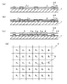
図1(a)は本発明のアライメント用の基板の実施の形態の第1の例の概略断面図を示した図で、図1(b)は本発明のアライメント用の基板の実施の形態の第2の例の概略断面図を示した図で、図1(c)は本発明のアライメント用の基板の実施の形態の第3の例の概略断面図を示した図で、図1(d)は、カラーフィルタ形成基板の画素の配列の1例を示した図で、図2(a)〜図2(h)は、図1(a)、図1(b)、図1(c)に、それぞれ、示す第1の実施の形態例〜第3の実施の形態例の作製工程を示した断面図で、図3(a)は本発明のアライメント用の基板のアライメントマーク部の位置検出方法の1例を示した概略断面図で、図3(b)はアライメントマーク部を図3(a)のA1方向からみた図で、図3(c)はアライメントマーク部の撮影画像を示した概略図で、図3(d)はアライメントマーク部の表面の断面形状を示した図で、図4(a)は本発明のアライメント用の基板のアライメントマーク部の位置検出を実施する概略構成の1例を示した図で、図4(b)は処理基板のアライメントマーク部とマスクのアライメントマークとを重ねて示した図で、図5は図4(a)に示すアライメント方法の処理の1例のフロー図で、図6は本発明のアライメント用の基板に関わるカラーフィルタ形成基板の作製方法、液晶表示パネルの作製の処理フローの1例を示した処理フロー図で、図7は図6に示すカラーフィルタ形成基板の作製方法により作製されたカラーフィルタ形成基板の1例を示した断面図で、図8は図6に示すカラーフィルタ形成基板の作製方法により作製されたカラーフィルタ形成基板の他の1例を示した断面図である。
尚、図1(a)〜図1(c)においては、分かり易くするため便宜上、第1の着色層〜第3の着色層の各着色層の数を少なく示してある。
また、図3(c)は、アライメントマーク部の頂部22aやエッジ底の面部22cは輝度が高く白部として示し、暗部20Bを斜線部として示しており、暗部20Bは濃淡があるが、ここでは便宜上このように示している。
また、図3(d)は、図3(b)のA2−A3における断面を示したものである。
また、図3(a)に示す撮像装置は簡略化して示されており、レンズ系は省略されている。
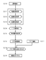
また、図5におけるS1〜S10、図6におけるS20〜S29は処理ステップを示している。
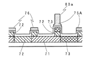
図1〜図8中、1は透明基板、2aは第1の着色層、2Aはマーク、3は着色樹脂層(着色層とも言う)、3Aはアライメントマーク部、3aは第2の着色層、4は着色樹脂層(着色層とも言う)、4Aはアライメントマーク部、4aは第3の着色層、5はITO膜、6は着色樹脂層(着色層とも言う)、6aは(ブラックストライプ用の)着色層、6Aはアライメントマーク部、6aはブラックストライプ、7はカラーフィルタ形成基板、8は画素配列、8aは画素領域、10は透明基板、10aは処理基板(カラーフィルタ形成用基板とも言う)、20はアライメントマーク部、20Aは(アライメントマーク部の)撮影画像、20Bは暗部、20Cはアライメントマーク部の位置、20Xはx方向のライン、20Yはy方向のライン、21は(着色層の)マーク、22は着色樹脂層(着色層とも言う)、22aは頂部、22bはテーパー部(エッジ部とも言う)、22cは面部(テーパー部の底側の面部とも言う)、30はマスク、31はアライメントマーク、35はマスク保持部、40は撮像装置、41はCCDエリアセンサ、42はハーフミラー、43は(照明用の)光源、44はミラー、50はステージ、55は基板保持部、71は1層目の着色層、72は2層目の着色層、73は3層目の着色層、74はITO膜、75はBM層(遮光性着色層とも言う)、75Aは半遮光性着色層、76はブラックマトリクス部(単にブラックマトリクスとも言う)、80、80aは柱状スペーサ、R0 は赤色画素部、G0 は緑色画素部、B0 は青色画素部である。
Embodiments of the present invention will be described with reference to the drawings.
FIG. 1A is a schematic cross-sectional view of a first example of an embodiment of an alignment substrate of the present invention, and FIG. 1B is an embodiment of the alignment substrate of the present invention. FIG. 1C is a diagram showing a schematic sectional view of the second example of the embodiment of the alignment substrate of the present invention, and FIG. 1D is a diagram showing a schematic sectional view of the second example. ) Is a diagram illustrating an example of the arrangement of pixels on the color filter forming substrate, and FIGS. 2A to 2H are FIGS. 1A, 1B, and 1C. FIGS. 3A and 3B are cross-sectional views showing manufacturing steps of the first to third embodiments shown in FIG. 3, respectively, and FIG. 3A shows the position detection of the alignment mark portion of the alignment substrate of the present invention. FIG. 3B is a schematic cross-sectional view showing an example of the method, FIG. 3B is a view of the alignment mark portion seen from the A1 direction of FIG. 3A, and FIG. FIG. 3D is a diagram showing a cross-sectional shape of the surface of the alignment mark portion, and FIG. 4A is a diagram of the alignment mark portion of the alignment substrate of the present invention. FIG. 4B is a diagram showing an example of a schematic configuration for performing position detection, FIG. 4B is a diagram in which the alignment mark portion of the processing substrate and the alignment mark of the mask are overlapped, and FIG. 5 is FIG. FIG. 6 is a flowchart showing an example of a process for producing a color filter forming substrate and a process flow for producing a liquid crystal display panel related to the alignment substrate of the present invention. 7 is a cross-sectional view showing an example of a color filter forming substrate manufactured by the method for manufacturing a color filter forming substrate shown in FIG. 6, and FIG. 8 is a manufacturing method of the color filter forming substrate shown in FIG. It is a sectional view showing a more further example of the produced color filter formation substrate.
In FIG. 1A to FIG. 1C, for the sake of simplicity, the number of the colored layers of the first colored layer to the third colored layer is reduced.
Further, in FIG. 3C, the top portion 22a of the alignment mark portion and the
FIG. 3D shows a cross section taken along line A2-A3 in FIG.
Further, the imaging apparatus shown in FIG. 3A is shown in a simplified manner, and the lens system is omitted.
Further, S1 to S10 in FIG. 5 and S20 to S29 in FIG. 6 indicate processing steps.
1 to 8, 1 is a transparent substrate, 2a is a first colored layer, 2A is a mark, 3 is a colored resin layer (also referred to as a colored layer), 3A is an alignment mark portion, 3a is a second colored layer, 4 is a colored resin layer (also referred to as a colored layer), 4A is an alignment mark portion, 4a is a third colored layer, 5 is an ITO film, 6 is a colored resin layer (also referred to as a colored layer), and 6a is (for black stripes) ) Colored layer, 6A is an alignment mark portion, 6a is a black stripe, 7 is a color filter forming substrate, 8 is a pixel array, 8a is a pixel region, 10 is a transparent substrate, 10a is a processing substrate (also called a color filter forming substrate) , 20 is an alignment mark portion, 20A is a captured image (of the alignment mark portion), 20B is a dark portion, 20C is a position of the alignment mark portion, 20X is a line in the x direction, 20Y is a line in the y direction, 1 is a mark (of a colored layer), 22 is a colored resin layer (also called a colored layer), 22a is a top portion, 22b is a tapered portion (also called an edge portion), and 22c is a surface portion (also called a bottom surface portion of the tapered portion). , 30 is a mask, 31 is an alignment mark, 35 is a mask holding unit, 40 is an imaging device, 41 is a CCD area sensor, 42 is a half mirror, 43 is a light source (for illumination), 44 is a mirror, 50 is a stage, 55 Is a substrate holding portion, 71 is a first colored layer, 72 is a second colored layer, 73 is a third colored layer, 74 is an ITO film, 75 is a BM layer (also referred to as a light-shielding colored layer), 75A is a semi-light-shielding colored layer, 76 is a black matrix portion (also simply referred to as a black matrix), 80 and 80a are columnar spacers, R 0 is a red pixel portion, G 0 is a green pixel portion, and B 0 is a blue pixel portion. .
本発明のアライメント用の基板の実施の形態例を図1に基づいて説明する。
図1(a)に示す第1の例のアライメント用の基板、図1(b)に示す第2の例のアライメント用の基板、図1(c)に示す第3の例のアライメント用の基板は、いずれも、
図1(d)に示すような同じ色の画素をストライプ状に配列した画素配列のカラーフィルタ形成基板を形成するための中間基板で、図1(d)では明示していないが、図2(h)に示されるように、第1の着色層2a、第2の着色層3a、第3の着色層4aをストライプ状に配し、且つ、各色の着色層の境部に黒色の着色層(ブラックマトリクス6aと言う)を配した断面構造のカラーフィルタ形成基板を形成する中間工程での基板です。
図1(a)に示す第1の例のアライメント用の基板は、第1の着色層2aと、該第1の着色層と同じ着色樹脂層から形成された着色層からなるマーク2Aを配設し、第1の着色層2a、マーク2Aを覆うように全面に第2の着色層を形成するための着色樹脂層3で覆った形態のものである。
第1の例では、アライメントマーク部3Aは、透明基板1の一面に配設された着色層からなるマーク2Aと、該マーク領域全体を覆い、該マークの形状に沿い盛り上がるように配設された着色樹脂層3とからなる。
アライメントマーク部3Aは、その領域を正反射照明(落射照明)にて撮像装置のCCDエリアセンサで撮影した画像から、画像処理により、該アライメントマーク部の位置を検出するためのものです。
図1(b)に示す第2の例のアライメント用の基板は、第1の着色層2aと、該第1の着色層と同じ着色樹脂層から形成された着色層からなるマーク2Aと、第2の着色層3aとを配設し、第1の着色層2a、マーク2A、第2の着色層3aを覆うように全面に第3の着色層を形成するための着色樹脂層4で覆った形態のものである。
第2の例では、アライメントマーク部4Aは、透明基板1の一面に配設された着色層からなるマーク2Aと、該マーク領域全体を覆い、該マークの形状に沿い盛り上がるように配設された着色樹脂層4とからなる。
アライメントマーク部4Aも、その領域を正反射照明(落射照明)にて撮像装置のCCDエリアセンサで撮影した画像から、画像処理により、該アライメントマーク部の位置を検出するためのものです。
図1(c)に示す第3の例のアライメント用の基板は、第1の着色層2aと、該第1の着色層と同じ着色樹脂層から形成された着色層からなるマーク2Aと、第2の着色層3aと、第3の着色層4aとを配設し、これらを覆うようにITO膜5を配設し、更に、
第1の着色層2a、マーク2A、第2の着色層3a、第3の着色層4aの領域を覆うようにITO膜5上全面にブラックマトリクス6aを形成するための着色樹脂層6で覆った形態のものである。
第3の例では、アライメントマーク部6Aは、透明基板1の一面に配設された着色層からなるマーク2Aと、該マーク領域全体を覆うITO膜5、更に、ITO膜5が覆われたマーク領域全体を覆い、該マークの形状に沿い盛り上がるように配設された着色樹脂層6とからなる。
アライメントマーク部6も、その領域を正反射照明(落射照明)にて撮像装置のCCDエリアセンサで撮影した画像から、画像処理により、該アライメントマーク部の位置を検出するためのものです。
尚、上記各アライメントマーク部3A、4A、6Aについては、各アライメントマーク部の、着色層からなるマーク2Aの幅を横切る断面のテーパー部(エッジ部とも言う)の平均傾きをθとした場合、tanθの値が0.028以上であることが好ましい。
先にも述べたが、十分にテーパー部(エッジ部)を認識するには、撮像装置のCCDエリアセンサが撮影する輝度の階調を0〜255までの256階調とした場合、撮影した際に暗くなるテーパー部(エッジ部)の輝度と、明るくなるアライメントマーク部の頂部やエッジ底の面部との輝度差が10以上であることが、実用レベルでは求められるが、上記tanθの値が0.028以上である場合に、輝度差を10以上とすることができることを意味する。
An embodiment of an alignment substrate according to the present invention will be described with reference to FIG.
The alignment substrate of the first example shown in FIG. 1 (a), the alignment substrate of the second example shown in FIG. 1 (b), and the alignment substrate of the third example shown in FIG. 1 (c). Are both
This is an intermediate substrate for forming a color filter forming substrate having a pixel array in which pixels of the same color as shown in FIG. 1D are arranged in a stripe pattern, which is not clearly shown in FIG. h), the first colored layer 2a, the second colored layer 3a, and the third colored layer 4a are arranged in a stripe shape, and a black colored layer ( This is a substrate in an intermediate process to form a color filter forming substrate with a cross-sectional structure with black matrix 6a).
The alignment substrate of the first example shown in FIG. 1A is provided with a first colored layer 2a and a mark 2A composed of a colored layer formed from the same colored resin layer as the first colored layer. And it is a thing of the form covered with the
In the first example, the alignment mark portion 3A is arranged so as to cover the entire mark area and the mark 2A made of a colored layer disposed on one surface of the
The alignment mark part 3A is for detecting the position of the alignment mark part by image processing from an image obtained by photographing the area with the CCD area sensor of the imaging device with specular reflection illumination (epi-illumination illumination).
The alignment substrate of the second example shown in FIG. 1B includes a first colored layer 2a, a mark 2A formed of a colored layer formed of the same colored resin layer as the first colored layer, 2 colored layers 3a and covered with a
In the second example, the alignment mark portion 4A is arranged so as to cover the entire mark area and to rise along the shape of the mark 2A formed of a colored layer disposed on one surface of the
The alignment mark portion 4A is also for detecting the position of the alignment mark portion by image processing from an image obtained by photographing the area with the CCD area sensor of the image pickup device with specular reflection illumination (epi-illumination illumination).
The alignment substrate of the third example shown in FIG. 1C includes a first colored layer 2a, a mark 2A composed of a colored layer formed of the same colored resin layer as the first colored layer, 2 colored layer 3a and third colored layer 4a are disposed,
The first colored layer 2a, the mark 2A, the second colored layer 3a, and the third colored layer 4a are covered with a
In the third example, the alignment mark portion 6A includes a mark 2A made of a colored layer disposed on one surface of the
The
In addition, for each of the alignment mark portions 3A, 4A, and 6A, when the average inclination of the tapered portion (also referred to as an edge portion) of the cross section across the width of the mark 2A made of the colored layer of each alignment mark portion is θ, The value of tan θ is preferably 0.028 or more.
As described above, in order to sufficiently recognize the taper portion (edge portion), when the gradation of luminance photographed by the CCD area sensor of the imaging apparatus is set to 256 gradations from 0 to 255, when photographing is performed. Although it is required on a practical level that the luminance difference between the brightness of the taper portion (edge portion) that becomes darker and the top portion of the alignment mark portion or the surface portion of the edge bottom that becomes brighter is 0, the value of tan θ is 0. If it is 0.028 or more, it means that the luminance difference can be 10 or more.
尚、透明基板10としては、低膨張で透明性の良いものが好ましく、ここではガラス基板を用いているが、これに限定されない。
プラスチック基板等も用いられる。
第1の着色層2a、第2の着色層3a、第3の着色層4aの各着色層を形成するための樹脂着色層としては、ここでは、それぞれ、紫外線硬化型の感光性樹脂に顔料や染料他を混ぜて分散させた、顔料分散型の着色材料を用いている。
第1の着色層2a、第2の着色層3a、第3の着色層4aの各着色層としては、通常、R(赤色)、G(緑色)、B(青色)の各色の着色層が用いられる。
The
A plastic substrate or the like is also used.
Here, as the resin colored layers for forming the colored layers of the first colored layer 2a, the second colored layer 3a, and the third colored layer 4a, respectively, an ultraviolet curable photosensitive resin, a pigment, A pigment-dispersed coloring material in which a dye or the like is mixed and dispersed is used.
As the colored layers of the first colored layer 2a, the second colored layer 3a, and the third colored layer 4a, usually colored layers of R (red), G (green), and B (blue) are used. It is done.
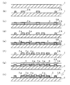
次に、第1の例〜第3の例のアライメント用の基板の作製工程と、これらを中間基板として作製されるカラーフィルタ形成基板の作製工程を、図2に基づいて、簡単に説明しておく。
透明基板1を用意しておき(図2(a))、その一面に第1の着色層2a形成用の感光性の着色樹脂層を一面に塗布し(図示していない)、該着色樹脂層を露光用のマスクを介して選択的に露光して、現像処理を施すフォトリソ法により、透明基板1の一面に第1の着色層2a、とマーク2Aとを形成する。(図2(b))
着色樹脂層としては、紫外線硬化型の感光性樹脂に顔料や染料他を混ぜて分散させたものが用いられる。
ここでの露光は、プロキシミティー露光が採られる。
この後、第1の着色層2a、マーク2Aを覆うように全面に第2の着色層を形成するための着色樹脂層3で塗布して覆い、第1の例のアライメント用の基板を作製する。(図2(c)) 次いで、該着色樹脂層3を露光用のマスクを介して選択的に露光して、現像処理を施すフォトリソ法により、透明基板1の一面に第2の着色層3aを更に形成する。(図2(d))
ここでも、着色樹脂層3としては、紫外線硬化型の感光性樹脂に顔料や染料他を混ぜて分散させたものが用いられ、露光は、プロキシミティー露光が採られる。
次いで、第1の着色層2aと、マーク2Aと、第2の着色層3aを覆うように全面に第3の着色層を形成するための着色樹脂層4を塗布して覆い、第2の例のアライメント用の基板を作製する。(図2(e))
この後、該着色樹脂層4を露光用のマスクを介して選択的に露光して、現像処理を施すフォトリソ法により、透明基板1の一面に第3の着色層4aを更に形成する。(図2(f))
ここでも、着色樹脂層4としては、紫外線硬化型の感光性樹脂に顔料や染料他を混ぜて分散させたものが用いられ、露光は、プロキシミティー露光が採られる。
次いで、スパッタリングによりITO膜5を各着色層2a、3a、4a、とマーク2Aを覆うように全面に形成した後、第1の着色層2a、マーク2A、第2の着色層3a、第3の着色層4aの領域を覆うようにITO膜5上全面にブラックマトリクス6aを形成するための着色樹脂層6を塗布して覆い、第3の例のアライメント用の基板を作製する。(図2(g))
ITO焼結体をターゲットとし、所定のスパッタリング条件の下で、スパッタリングすることにより、処理基板の各着色層上にITO膜を単層膜として形成する。
この後、該着色樹脂層6を露光用のマスクを介して選択的に露光して、現像処理を施すフォトリソ法により、各着色層の境部にブラックマトリクス6aを更に形成する。(図2(h))
ここでも、着色樹脂層6としては、紫外線硬化型の感光性樹脂に顔料や染料他を混ぜて分散させたものが用いられ、露光は、プロキシミティー露光が採られる。
このようにして、図2(h)に示すカラーフィルタ形成基板7が形成される。
Next, the manufacturing process of the alignment substrate according to the first to third examples and the manufacturing process of the color filter forming substrate manufactured using these as an intermediate substrate will be briefly described with reference to FIG. deep.
A
As the colored resin layer, an ultraviolet curable photosensitive resin in which pigments, dyes, and the like are mixed and dispersed is used.
The exposure here is proximity exposure.
Thereafter, the first colored layer 2a and the mark 2A are coated and covered with the
Here, as the
Next, a
Thereafter, the
Here, as the
Next, after forming the
An ITO film is formed as a single layer film on each colored layer of the treatment substrate by sputtering under a predetermined sputtering condition using an ITO sintered body as a target.
Thereafter, the
Here, as the
In this way, the color
次に、本発明のアライメント用の基板のアライメントマーク部の位置検出方法の1例を、図3に基づいて説明する。
本例のアライメントマーク部の位置検出方法は、カラーフィルタ形成基板の作製における着色層のパターニングの際に採られる、アライメントマーク部の位置検出方法で、透明基板10の一面に、R、G、Bの1色からなる着色層からなるマーク21と、該マーク21を覆うように塗布された、マーク部の色とは異なるR、G、Bの1色からなる着色樹脂層(着色層とも言う)1層22とからなり、該着色樹脂層22が前記マーク21に沿い盛り上がった領域を含む部分を、アライメントマーク部20とし、該アライメントマーク部20の前記マーク21の位置を検出するための、アライメントマーク部20のマーク位置検出方法である。
そして、撮像装置40により、レンズ系(図示されていない)を介してCCDエリアセンサ41により、前記アライメントマーク部20を含む領域を撮影した画像から、画像処理により、該アライメントマーク部の位置を検出するものである。
特に、本例においては、撮像装置40による撮影を、アライメントマーク部20を含む領域を、正反射照明(落射照明)にて撮影するもので、これにより、このような構造のアライメントマーク部20の、マーク21に沿い盛り上がった領域の形状、特にアライメントマーク部20のマーク21の位置を認識できるものとしている。
ここでは、アライメントマーク部20の位置を検出し、これをもってマーク21の位置とするが、これは、先にも述べたが、アライメントマーク部の表面を撮影してその形状が十分に認識できれば、着色層からなるマークのセンター位置(単にマーク位置とも言う)が、撮影されたアライメントマーク部のセンター位置に相当するという認識のもとに、正反射照明(落射照明)にて撮影することにより、アライメントマーク部の表面を撮影することによりその形状が十分に認識できることによるもので、このようにしてアライメントマーク部20のマーク21の位置を検出することにより、実質的にマーク21の位置検出を実用レベルでできるものとしている。
Next, an example of the position detection method of the alignment mark portion of the alignment substrate according to the present invention will be described with reference to FIG.
The position detection method of the alignment mark part of this example is a position detection method of the alignment mark part, which is adopted when patterning the colored layer in the production of the color filter forming substrate. On one surface of the
Then, the position of the alignment mark part is detected by image processing from an image obtained by photographing the area including the
In particular, in this example, the
Here, the position of the
先ず、図3(a)に示すように、処理基板10aのアライメントマーク部の位置に、撮像装置40をセットし、また、照明光の光源をセットする。
次いで、撮像装置にて、アライメントマーク部20を照明光の落下照明にて撮影する。 図3(a)に示すように、光源からの照明光は、撮像装置のハーフミラー42を介して反射され、アライメントマーク部20に落下照明される。
撮影の際、落下照明によるライメントマーク部20からの反射光は、撮像装置のハーフミラー42を通過して、CCDエリアセンサ41に入射される。
ここでは、マーク21は十字形状で、図3(a)に示すように、アライメントマーク部20は、マーク形状に沿い十字形状に盛り上がっており、頂部22a、テーパ部(エッジ部)22bを有する形状となっているため、頂部22aでは、反射光の強度は大きく、テーパ部(エッジ部)では小さく、またテーパ底(エッジ底)の面部22cでは大きくなるため、このように、落下照明された光の反射光でアライメントマーク部20(図3(b)参照)を撮影した画像は、図3(c)のように、頂部22aとエッジ底の面部22cは明るく、エッジ部は暗くなる。
図3(b)のA2−A3における断面の外形形状は、図3(d)のようになるが、エッジ部22bの平均傾きをθとした場合、tanθの値が0.028以上である場合には、実用レベルで良く認識できる。
尚、平均傾きは、概略的に、図3(d)に示すように、テーパ部(エッジ部)22bの底の勾配が緩やかな立ち上がり部、頂点付近の勾配が緩やかな部分を除いた領域の平均勾配としている。
First, as shown in FIG. 3A, the
Then, the
At the time of shooting, the reflected light from the
Here, the
The outer shape of the cross section at A2-A3 in FIG. 3B is as shown in FIG. 3D, but when the average inclination of the edge portion 22b is θ, the value of tan θ is 0.028 or more. Can be recognized well at a practical level.
In addition, the average inclination is roughly shown in FIG. 3 (d) in the region excluding the rising part where the slope of the taper part (edge part) 22b is gentle and the part where the slope near the apex is gentle. Average slope.
アライメントマーク部20の撮影後、画像処理部により、アライメントマーク部20を撮影した画像(図3(c)参照)を用いて、これを処理して、例えば、x方向のライン20Xの中心y位置とy方向ライン20Yの中心y位置とからアライメントマーク部20の位置(x、y)を求め、マーク21の位置として検出する。
このようにして、アライメントマーク部20のマーク21の位置を求める。
画像処理については、例えば、階調表示された撮影画像(図3(c)参照)の画像データに対して、各画素毎に所定のスライスレベルで2値化して、暗いテーパ部(エッジ部)を黒、アライメントマーク部20の頂部22aやテーパ底(エッジの底)の面部22c等の明るい部分を白とした2値化画像データを得た後、更に、得られた2値化画像データから、x方向のラインの中心y位置とy方向ラインの中心位置とを求める。
ここでは、これをアライメントマーク部20の位置で、実質的にマーク21の位置の想到する。
撮影画像について、各画素の近傍領域について平滑化処理した平滑化画像データを得て、この画像データに対して各画素毎に所定のスライスレベルで2値化して、暗いテーパ部(エッジ部)を黒、アライメントマーク部20の頂部22aやテーパの底(エッジの底)の面部22c等の明るい部分を白とした2値化画像データを得た後、更に、得られた2値化画像データから、x方向のラインの中心y位置とy方向ラインの中心位置とを求めても良い。
尚、ここでの平滑化処理は、例えば、原画像(撮影画像)データの各画素に対して、それぞれ、画素の近傍領域内の全画素のヒストグラムの中心値を新たな画素値として、新たな画像データを得て、これを平滑化画像データとするものです。
After photographing the
In this way, the position of the
For image processing, for example, image data of a photographic image displayed in gradation (see FIG. 3C) is binarized at a predetermined slice level for each pixel, and a dark tapered portion (edge portion) is obtained. Obtained from the binarized image data in which the bright portion such as the top portion 22a of the
Here, this is the position of the
With respect to the captured image, smoothed image data obtained by performing a smoothing process on the vicinity region of each pixel is obtained, and this image data is binarized at a predetermined slice level for each pixel, and a dark tapered portion (edge portion) is obtained. After obtaining binarized image data in which the bright portions such as black, the top portion 22a of the
Note that the smoothing process here is, for example, a new pixel value for each pixel of the original image (captured image) data, with the center value of the histogram of all the pixels in the vicinity region of the pixel as a new pixel value. Image data is obtained and used as smoothed image data.
照明用の光源43としては、例えば、マークが赤(R)色の着色層からなり、これを覆う樹脂着色層の色が青(B)色の場合は、赤外LEDを用いる。
CCDエリアセンサ41を備えた撮像装置として、特に限定されない。
As the
The imaging device including the CCD area sensor 41 is not particularly limited.
次に、本発明のアライメント用の基板のアライメントマーク部の位置検出方法を用いた、アライメント方法の1例を、図4、図5に基づいて更に説明する。
ここでは、図3にて説明したアライメントマーク部の位置検出方法が、透明基板の一面に、各色の着色層からなる各色のカラーフィルタ部、着色層からなるBMを有し、柱部(スペーサとも言う)を、各カラーフィルタ部やBM部を形成するための着色層で形成し、且つ、各色のカラーフィルタ部上にITO層を配している、TN方式(Twisted Nematic mode)の液晶表示パネル用のカラーフィルタ形成基板を作製する際、着色層のフォトリソ工程におけるアライメントに適用されたものとする。
アライメントは、図4(a)に示すような装置構成でなされる。
図4に示す処理基板10aは、着色層からなるマーク21を有するアライメントマーク部20(図3参照)を、処理基板10aの2箇所に備えておき、露光用のマスク30の対応する2箇所のアライメントマーク31と、それぞれ、アライメントを行うものです。
ここでは、処理基板10aは、その位置座標が管理されているステージ55上に固定された基板保持部55にて保持された状態で、マスク保持部35により位置固定されたプロキシミティー露光を行うための露光用のマスク30と所定のギャップ間隔とをあけている。
そして、処理基板10aの各アライメントマーク部20を、露光用のマスク30の対応するアライメントマーク31と、それぞれ、粗く位置あわせし、露光用のマスク30の2箇所のアライメントマーク31を撮影できる位置に、それぞれ、図3(a)に示す構成の撮像装置40、光源部43をセットしておく。(S1〜S2)
この後、各撮像装置40により、各位置で、それぞれ、マスク30の各アライメントマークを撮影して、その座標位置(ステージを管理する座標位置)での撮影画像として取り込む。(S3)
一方、その座標位置で、各撮像装置40により、処理基板10aのアライメントマーク部20を、先に述べた図3の説明のようにして撮影して、その座標位置(ステージを管理する座標位置)での撮影画像として取り込む。(S4)
ここでは、図4(b)に示すような形状のアライメントマーク31、マーク21が用いられる。
次いで、図3について先に説明したアライメントマーク部の位置検出方法により、撮影により得られたマスク30の各アライメントマーク31の画像データDm1、Dm2、処理基板10aの各アライメントマーク部20の画像データDa1、Da2から、それぞれ、各アライメントマーク31、各アライメントマーク部20の位置を検出する。(S4〜S5、S7〜S8)
図4(b)では、各アライメントマークのx方向、y方向のセンター位置をその位置としている。
各対応する位置でのアライメントマーク31とアライメントマーク部20との位置ずれを算出して抽出する。(S9)
次いで、抽出された各位置のずれ量に基づいて、これを補正するような、ステージ移動量を算出し、算出された結果に基づいてステージ移動を行う。(S10)
このようにして、マスク30と処理基板10aとのアライメントがなされる。
Next, an example of an alignment method using the position detection method of the alignment mark portion of the alignment substrate according to the present invention will be further described with reference to FIGS.
Here, the alignment mark portion position detection method described in FIG. 3 has a color filter portion composed of a colored layer of each color and a BM composed of a colored layer on one surface of a transparent substrate. TN type (twisted nematic mode) liquid crystal display panel, which is formed with a colored layer for forming each color filter portion and BM portion, and an ITO layer is disposed on the color filter portion of each color When producing a color filter forming substrate for use, it is applied to alignment in a photolithography process of a colored layer.
The alignment is performed with an apparatus configuration as shown in FIG.
The
Here, the
Then, each
Thereafter, each
On the other hand, at each of the coordinate positions, each
Here, alignment marks 31 and 21 having shapes as shown in FIG. 4B are used.
Next, the image data Dm1 and Dm2 of each
In FIG. 4B, the center position of each alignment mark in the x and y directions is the position.
The positional deviation between the
Next, based on the extracted displacement amount of each position, a stage movement amount that corrects this is calculated, and the stage movement is performed based on the calculated result. (S10)
In this way, alignment between the mask 30 and the
次に、本発明のアライメントマーク部の位置検出方法を用いたアライメント方法を採り入れた、カラーフィルタ形成基板の作製方法の1例を、説明する。
本例は、透明基板の一面に、各色の着色層からなる各色のカラーフィルタ部、着色層からなるBMを有し、柱部(スペーサとも言う)を、各カラーフィルタ部やBM部を形成するための着色層で形成し、且つ、各色のカラーフィルタ部上にITO層を配している、TN方式(Twisted Nematic mode)の液晶表示パネル用のカラーフィルタ形成基板を作製する、カラーフィルタ形成基板の作製方法で、前記透明基板の一面に各着色層を形成するための感光性着色樹脂を塗布し、フォトマスクを介して選択的に露光を行い、現像することにより、所望の形状に各着色層を形成する、フォトリソ工程を、形成する着色層の数だけ行い、前記各カラーフィルタ部、ブラックマトリクス部(BM部とも言う)、柱部(スペーサとも言う)を形成するものです。
前記各フォトリソ工程における、露光は、前記透明基板の他面をステージ(載置台)側にして載せ、フォトマスクを介してプロキシミティー露光方法にて行うもので、前記複数回行うフォトリソ工程における、2回目以降の各フォトリソ工程の際のアライメントは、図4にて説明したアライメント方法を採るもので、前記透明基板側に設けられたアライメントマーク部と、露光用のフォトマスクのCr等の遮光層からなるアライメントマーク部とを用い、各アライメントマーク部を、前記フォトマスクの光源側に設けられた撮像装置により、レンズ系を介してCCD等の画素分割のエリアセンサにより、アライメントマーク部領域を含む領域を撮影した画像から、画像処理により、その位置を検出して、検出された位置に対応して、相対的にフォトマスクと透明基板側を位置移動して、行うものであり、且つ、1回目のフォトリソ工程により形成された着色層からなるマークと、該マークを覆う、2回目以降の各フォトリソ工程において塗布される着色層を形成するための感光性着色樹脂からなる着色樹脂層1層とを、前記アライメントマーク部とし、該アライメントマーク部を、正反射照明(落射照明)にて、前記撮像装置により撮影するものである。
Next, an example of a method for producing a color filter forming substrate, which employs an alignment method using the alignment mark position detection method of the present invention, will be described.
In this example, a color filter portion of each color composed of a colored layer of each color and a BM composed of a colored layer are provided on one surface of a transparent substrate, and a column portion (also referred to as a spacer) is formed on each color filter portion and BM portion. A color filter forming substrate for producing a color filter forming substrate for a liquid crystal display panel of a TN mode (Twisted Nematic mode), which is formed of a colored layer for forming a color filter and an ITO layer is disposed on a color filter portion of each color The photosensitive coloring resin for forming each colored layer is applied on one surface of the transparent substrate, selectively exposed through a photomask, and developed, whereby each color is formed into a desired shape. The photolithography process for forming the layers is performed by the number of the colored layers to be formed, and each color filter portion, black matrix portion (also referred to as BM portion), column portion (also referred to as spacer). ) It is intended to form.
The exposure in each of the photolithographic steps is performed by a proximity exposure method through a photomask, with the other surface of the transparent substrate being placed on the stage (mounting table) side. Alignment at the time of each photolithography process after the first time is the alignment method described in FIG. 4, and includes an alignment mark portion provided on the transparent substrate side and a light shielding layer such as Cr of a photomask for exposure. Each of the alignment mark portions including an alignment mark portion region by an image sensor provided on the light source side of the photomask and an area sensor of pixel division such as a CCD through a lens system. The position is detected from the captured image by image processing, and relative to the detected position This is performed by moving the position of the photomask and the transparent substrate, and is formed by a colored layer formed by the first photolithographic process, and is applied in each of the second and subsequent photolithographic processes covering the mark. A colored resin layer made of a photosensitive colored resin for forming a colored layer is used as the alignment mark portion, and the alignment mark portion is photographed by the imaging device with specular illumination (epi-illumination). It is.
上記カラーフィルタ形成基板およびこれを用いた液晶表示パネルの作製方法は、例えば、図6に示す処理フローで行われる。
簡単には、先ず、透明基板の一面に1層目として赤色のR層をフォトリソ形成する。(S20〜S21)
透明基板10としては、低膨張で透明性の良いものが好ましく、ここではガラス基板を用いているが、これに限定されない。
プラスチック基板等も用いられる。
この際、マーク(図3の21に相当)を形成しておく。
次いで、青色のB層形成用の感光性の樹脂着色層を、前記マーク上も含め処理基板を覆うように塗布し、乾燥後、上記、図4、図5に基づいて説明したアライメントマーク部の位置検出方法を用いたアライメント方法により、アライメントして、露光を行い、現像して、2層目のB層を形成する。(S22)
次いで、同様に、緑色のG層形成用の感光性の樹脂着色層を、前記マーク上も含め処理基板を覆うように塗布し、乾燥後、上記、図4、図5に基づいて説明したアライメントマーク部の位置検出方法を用いたアライメント方法により、アライメントして、露光を行い、現像して、3層目のG層を形成する。(S23)
R層形成処理(S21)は、紫外線硬化型の感光性樹脂に顔料や染料他を混ぜて分散させた赤色の着色層を、透明基板10の一面に塗布してフォトリソ法により、所定形状にして、1層目の着色層(赤色の着色層、R層とも言う)を所定の領域に形成する。
同様に、B層形成処理(S22)は、紫外線硬化型の感光性樹脂に顔料や染料他を混ぜて分散させた青色の着色層を、透明基板10の1層目の着色層が形成された側の面に塗布してフォトリソ法により、所定形状にして、2層目の着色層(青色の着色層、B層とも言う)を所定の領域に形成する。
また同様に、G層形成処理(S23)は、紫外線硬化型の感光性樹脂に顔料や染料他を混ぜて分散させた緑色の着色層を、透明基板10の1層目の着色層、2層目の着色層が形成された側の面に塗布してフォトリソ法により、所定形状にして、第3の着色層(緑色の着色層、G層とも言う)を形成する。
The color filter forming substrate and a method for manufacturing a liquid crystal display panel using the color filter forming substrate are performed, for example, by a processing flow shown in FIG.
In brief, first, a red R layer is formed as a first layer on one surface of a transparent substrate by photolithography. (S20-S21)
As the
A plastic substrate or the like is also used.
At this time, a mark (corresponding to 21 in FIG. 3) is formed.
Next, a photosensitive resin colored layer for forming a blue B layer is applied so as to cover the processing substrate including the mark, and after drying, the alignment mark portion described with reference to FIGS. 4 and 5 is used. Alignment is performed by an alignment method using a position detection method, exposure is performed, and development is performed to form a second B layer. (S22)
Next, similarly, a photosensitive resin colored layer for forming a green G layer is applied so as to cover the processing substrate including the mark, and after drying, the alignment described with reference to FIGS. 4 and 5 above. Alignment is performed by an alignment method using the mark position detection method, exposure is performed, and development is performed to form a third G layer. (S23)
In the R layer forming process (S21), a red colored layer in which a pigment, a dye, or the like is mixed and dispersed in an ultraviolet curable photosensitive resin is applied to one surface of the
Similarly, in the B layer forming process (S22), the first colored layer of the
Similarly, in the G layer forming process (S23), a green colored layer obtained by mixing and dispersing a pigment, a dye, or the like in an ultraviolet curable photosensitive resin is used as the first colored layer, two layers of the
次いで、ITO焼結体をターゲットとし、所定のスパッタリング条件の下で、スパッタリングすることにより、処理基板の各着色層上にITO膜を単層膜として形成する。(S24)
制御用電極用のITO膜を形成するためのスパッタリングは、一般には、Arガス雰囲気中、1×10⁻⁵torr〜1×10⁻²torr圧下において、成膜する膜組成(例えば、In2 O3 、90w%+SnO2 、10w%組成)で、厚さ8mm〜15mmのITO焼結体をターゲット材として用いて、直流マグネトロンスパッタ方式で行っている。
ターゲットとしては、通常、Cuプレートをバッキング材として、インジウム半田を接着層とし、多数枚の焼結ターゲット材をつなぎ合わせて、1つのターゲットプレートとしたものが用いられている。
尚、制御用電極としてITO膜を配設するカラーフィルタ形成基板の作製においては、カラーフィルタを形成する着色層上に、スパッタリングにてITO膜を形成するため、カラーフィルタを形成する着色層の耐熱性、カラーフィルタを形成する着色層からの脱ガスの面から、低温で成膜を行うことが求められている。
Next, an ITO film is formed as a single layer film on each colored layer of the processing substrate by sputtering under a predetermined sputtering condition using an ITO sintered body as a target. (S24)
Sputtering for forming an ITO film for a control electrode is generally performed in a film composition (for example, In 2 O) under an Ar gas atmosphere under a pressure of 1 × 10 −5 torr to 1 × 10 −2 torr. 3 , 90 w% + SnO 2 , 10 w% composition), and an ITO sintered body having a thickness of 8 mm to 15 mm is used as a target material, and the direct current magnetron sputtering method is used.
As the target, a target plate is usually used in which a Cu plate is used as a backing material, indium solder is used as an adhesive layer, and a large number of sintered target materials are joined together.
In the production of a color filter forming substrate in which an ITO film is disposed as a control electrode, the ITO film is formed by sputtering on the colored layer forming the color filter. In view of the property and degassing from the colored layer forming the color filter, it is required to form the film at a low temperature.
次いで、2層目、3層目の着色層形成と同様に、黒色のBM層形成用の感光性の樹脂着色層を、前記マーク上も含め処理基板を覆うように塗布し、乾燥後、上記、図2、図3に基づいて説明した本発明のアライメントマーク部の位置検出方法を用いたアライメント方法により、アライメントして、露光を行い、現像して、BM層を形成する。(S25)
このようにしてカラーフィルタ形成基板(CF基板とも言う)が形成される。(S26)
Next, similar to the formation of the second and third colored layers, a photosensitive resin colored layer for forming a black BM layer is applied so as to cover the processing substrate including the mark, and after drying, the above-mentioned Alignment, exposure, and development are performed by the alignment method using the alignment mark position detection method of the present invention described with reference to FIGS. 2 and 3 to form a BM layer. (S25)
In this way, a color filter forming substrate (also referred to as a CF substrate) is formed. (S26)
このようにして形成されるカラーフィルタ形成基板は、例えば、図7に示すような形状をしている。
ここでは、柱状スペーサ80は、各着色層の形成の際、各色の着色層を積層するように、形成される。
また、BM層が最上層となっている。
尚、各色の着色層を厚みを変化させて形成するために、ここでは、先に説明した、透明基板の一面に転写時の露光光を遮光する遮光膜と、前記露光光に対して半透過性のハーフトーン膜とを、それぞれパターニングして配し、遮光膜が配設された遮光領域と、遮光膜はなくハーフトーン膜が配設されたハーフトーン領域と、遮光膜とハーフトーン膜のいずれもが存在しない透明領域とを、設けた階調マスクを用いる。
The color filter forming substrate formed in this way has a shape as shown in FIG. 7, for example.
Here, the
The BM layer is the top layer.
In order to form the colored layer of each color by changing the thickness, here, the light-shielding film that shields the exposure light at the time of transfer onto one surface of the transparent substrate and the semi-transmissive to the exposure light are described here. A halftone film having a light-shielding film, a halftone area in which there is no light-shielding film and a halftone film is provided, and a light-shielding film and a halftone film. A gradation mask provided with a transparent region in which none exists is used.
このようにして作製されたカラーフィルタ形成基板(S26)と、液晶パネル形成のためにこれと貼り合わせを行うTFT基板(S27)とを予め用意しておく。
そして、本例のカラーフィルタ形成基板透明導電膜形成基板110の外周のシール領域に、例えば、ディスペンサーあるいは印刷により、紫外線硬化型のシール材を塗布して、所定の高さにして、枠状のスペーサを形成し、更に、該枠状のスペーサ内に液晶を滴下法により配した後、TFT基板との貼り合わせを行う。(S28)
貼り合わせの際、カラーフィルタ形成基板の透明基板(図3の10に相当)側からシール領域のシール材に紫外線を照射して、シール材を硬化する。
このようにして、本例のカラーフィルタ形成基板を用いた液晶表示パネルは作製される。(S29)
A color filter forming substrate (S26) thus prepared and a TFT substrate (S27) to be bonded to form a liquid crystal panel are prepared in advance.
Then, an ultraviolet curable sealing material is applied to the outer peripheral sealing region of the color filter forming substrate transparent conductive film forming substrate 110 of this example by, for example, a dispenser or printing to obtain a predetermined height. A spacer is formed, and liquid crystal is disposed in the frame-like spacer by a dropping method, and then bonded to the TFT substrate. (S28)
At the time of bonding, the sealing material is cured by irradiating the sealing material in the sealing region with ultraviolet rays from the transparent substrate (corresponding to 10 in FIG. 3) side of the color filter forming substrate.
In this manner, a liquid crystal display panel using the color filter forming substrate of this example is manufactured. (S29)
尚、上記カラーフィルタ形成基板の作製方法は1例で、これらに限定されるものではない。
例えば、図7に示すBM層による遮光に代え、図8に示すように、R、G、Bの各着色層と半遮光性(灰色)の着色層による遮光でブラックマトリクス部や柱部を形成しても良い。
この場合の作製も基本的には、上記図6の説明の作製方法と同じで、各R、G、Bの各着色の形成の際、柱状スペーサ80aやブラックマトリクス部76を作製する。
この場合も、各色の着色層やを厚みを変化させて形成するために、ここでは、先に説明した、透明基板の一面に転写時の露光光を遮光する遮光膜と、前記露光光に対して半透過性のハーフトーン膜とを、それぞれパターニングして配し、遮光膜が配設された遮光領域と、遮光膜はなくハーフトーン膜が配設されたハーフトーン領域と、遮光膜とハーフトーン膜のいずれもが存在しない透明領域とを、設けた階調マスクを用いる。
また、着色画素の配列についても、各着色層をストライプ状に配置する上記のストライプ型以外にも、公知のモザイク型や、トライアングル型等の各種配列にも適用できる。
In addition, the manufacturing method of the said color filter formation board | substrate is an example, and is not limited to these.
For example, instead of the light shielding by the BM layer shown in FIG. 7, as shown in FIG. 8, the black matrix part and the column part are formed by the light shielding by the R, G, B colored layers and the semi-light-shielding (gray) colored layer. You may do it.
The fabrication in this case is basically the same as the fabrication method described with reference to FIG. 6, and the columnar spacer 80a and the
Also in this case, in order to form the colored layers of the respective colors with varying thicknesses, here, the light shielding film that shields the exposure light at the time of transfer onto one surface of the transparent substrate, and the exposure light described above are used. The semi-transparent halftone film is patterned and arranged, and the light-shielding area provided with the light-shielding film, the halftone area provided with the half-tone film without the light-shielding film, the light-shielding film and the half-tone film A gradation mask provided with a transparent region where none of the tone films exists is used.
Further, the arrangement of the colored pixels can be applied to various arrangements such as a known mosaic type and a triangle type in addition to the stripe type in which each colored layer is arranged in a stripe shape.
1 透明基板
2a 第1の着色層
2A マーク
3 着色樹脂層(着色層とも言う)
3A アライメントマーク部
3a 第2の着色層
4 着色樹脂層(着色層とも言う)
4A アライメントマーク部
4a 第3の着色層
5 ITO膜
6 着色樹脂層(着色層とも言う)
6a (ブラックストライプ用の)着色層
6A アライメントマーク部
6a ブラックストライプ
7 カラーフィルタ形成基板
8 画素配列
8a 画素領域
10 透明基板
10a 処理基板(カラーフィルタ形成用基板とも言う)
20 アライメントマーク部
20A (アライメントマーク部の)撮影画像
20B 暗部
20C アライメントマーク部の位置
20X x方向のライン
20Y y方向のライン
21 (着色層の)マーク
22 着色樹脂層(着色層とも言う)
22a 頂部
22b テーパー部(エッジ部とも言う)
22c 面部(テーパー部の底側の面部とも言う)
30 マスク
31 アライメントマーク
35 マスク保持部
40 撮像装置
41 CCDエリアセンサ
42 ハーフミラー
43 (照明用の)光源
44 ミラー
50 ステージ
55 基板保持部
71 1層目の着色層
72 2層目の着色層
73 3層目の着色層
74 ITO膜
75 BM層(遮光性着色層とも言う)
75A 半遮光性着色層
76 ブラックマトリクス部(単にブラックマトリクスとも言う)
80、80a 柱状スペーサ
R0 赤色画素部
G0 緑色画素部
B0 青色画素部
DESCRIPTION OF
3A Alignment mark portion 3a Second
4A Alignment mark portion 4a Third
6a Colored layer 6A (for black stripe) Alignment mark portion
20 Alignment mark portion 20A Captured image 20B (of alignment mark portion) Dark portion 20C Alignment mark portion position 20X x-direction line 20Y y-direction line 21 (of colored layer)
22a Top 22b Taper (also called edge)
22c surface portion (also referred to as a bottom surface portion of the tapered portion)
30
75A Semi-light-shielding
80, 80a Columnar spacer R 0 Red pixel portion G 0 Green pixel portion B 0 Blue pixel portion
Claims (4)
Priority Applications (1)
| Application Number | Priority Date | Filing Date | Title |
|---|---|---|---|
| JP2008258537A JP5513729B2 (en) | 2008-10-03 | 2008-10-03 | Method for producing color filter forming substrate |
Applications Claiming Priority (1)
| Application Number | Priority Date | Filing Date | Title |
|---|---|---|---|
| JP2008258537A JP5513729B2 (en) | 2008-10-03 | 2008-10-03 | Method for producing color filter forming substrate |
Publications (2)
| Publication Number | Publication Date |
|---|---|
| JP2010091607A true JP2010091607A (en) | 2010-04-22 |
| JP5513729B2 JP5513729B2 (en) | 2014-06-04 |
Family
ID=42254417
Family Applications (1)
| Application Number | Title | Priority Date | Filing Date |
|---|---|---|---|
| JP2008258537A Active JP5513729B2 (en) | 2008-10-03 | 2008-10-03 | Method for producing color filter forming substrate |
Country Status (1)
| Country | Link |
|---|---|
| JP (1) | JP5513729B2 (en) |
Citations (9)
| Publication number | Priority date | Publication date | Assignee | Title |
|---|---|---|---|---|
| JPH0443562B2 (en) * | 1985-06-25 | 1992-07-17 | Seikosha Kk | |
| JPH05196946A (en) * | 1992-01-20 | 1993-08-06 | Sharp Corp | Liquid crystal display device |
| JPH0674714A (en) * | 1992-08-28 | 1994-03-18 | Yamatake Honeywell Co Ltd | Substrate position detecting method |
| JPH08128811A (en) * | 1994-10-31 | 1996-05-21 | Sony Corp | Apparatus and method for detecting reference position |
| JP2003014917A (en) * | 2001-06-28 | 2003-01-15 | Toray Ind Inc | Color filter and liquid crystal display device |
| JP2003084120A (en) * | 2001-09-14 | 2003-03-19 | Dainippon Printing Co Ltd | Method for manufacturing color filter |
| JP2003215321A (en) * | 2003-01-23 | 2003-07-30 | Sharp Corp | Method for manufacturing color filter, and alignment mark |
| JP2007132857A (en) * | 2005-11-11 | 2007-05-31 | Seiko Epson Corp | Image processing apparatus and method, drawing device, electrooptical device method for fabricating same, and electronic device |
| JP2008251158A (en) * | 2005-04-28 | 2008-10-16 | Sharp Corp | Recording/reproducing device |
-
2008
- 2008-10-03 JP JP2008258537A patent/JP5513729B2/en active Active
Patent Citations (9)
| Publication number | Priority date | Publication date | Assignee | Title |
|---|---|---|---|---|
| JPH0443562B2 (en) * | 1985-06-25 | 1992-07-17 | Seikosha Kk | |
| JPH05196946A (en) * | 1992-01-20 | 1993-08-06 | Sharp Corp | Liquid crystal display device |
| JPH0674714A (en) * | 1992-08-28 | 1994-03-18 | Yamatake Honeywell Co Ltd | Substrate position detecting method |
| JPH08128811A (en) * | 1994-10-31 | 1996-05-21 | Sony Corp | Apparatus and method for detecting reference position |
| JP2003014917A (en) * | 2001-06-28 | 2003-01-15 | Toray Ind Inc | Color filter and liquid crystal display device |
| JP2003084120A (en) * | 2001-09-14 | 2003-03-19 | Dainippon Printing Co Ltd | Method for manufacturing color filter |
| JP2003215321A (en) * | 2003-01-23 | 2003-07-30 | Sharp Corp | Method for manufacturing color filter, and alignment mark |
| JP2008251158A (en) * | 2005-04-28 | 2008-10-16 | Sharp Corp | Recording/reproducing device |
| JP2007132857A (en) * | 2005-11-11 | 2007-05-31 | Seiko Epson Corp | Image processing apparatus and method, drawing device, electrooptical device method for fabricating same, and electronic device |
Also Published As
| Publication number | Publication date |
|---|---|
| JP5513729B2 (en) | 2014-06-04 |
Similar Documents
| Publication | Publication Date | Title |
|---|---|---|
| US10866452B2 (en) | Color filter substrate, production method thereof, display panel, and display apparatus | |
| WO2016173210A1 (en) | Manufacturing method for black matrix | |
| US20050134763A1 (en) | Liquid crystal display device and method of fabricating the same | |
| KR20000047768A (en) | Liquid Crystal Display Device and Method for Fabricating the Same | |
| CN106933023A (en) | A kind of preparation method of light shield and substrate of glass | |
| US10365523B2 (en) | Display panel and manufacturing method based on BOA technology | |
| CN104166177B (en) | Raster, manufacturing method of raster, display substrate and display device | |
| CN108363233A (en) | Colored filter substrate and preparation method thereof | |
| CN106526953A (en) | Method for manufacturing color filter layer substrate | |
| US20180188597A1 (en) | Color filter substrate, method for manufacturing the same and display device | |
| WO2014134886A1 (en) | Color filter substrate, manufacturing method therefor, and liquid crystal display screen | |
| US20030147115A1 (en) | Substrate for electrooptical device, method for manufacturing the substrate, electrooptical device, method for manufacturing the electrooptical device, and electronic apparatus | |
| WO2022166451A1 (en) | Color film substrate and manufacturing method therefor, and display panel | |
| US20070139587A1 (en) | Transflective liquid crystal display panel, color filter and fabricating method thereof | |
| TWI274906B (en) | A color filter | |
| JP4957020B2 (en) | Manufacturing method of color filter for liquid crystal display device and color filter for liquid crystal display device | |
| US7438947B2 (en) | Color filter process | |
| CN1888957B (en) | Color filter for liquid crystal display device | |
| US10824026B2 (en) | Substrate and preparation method therefor, and display panel | |
| WO2020107537A1 (en) | Display panel and manufacturing method therefor, and display apparatus | |
| KR20010007310A (en) | Liquid crystal display device and method for fabricating the same | |
| JP5513729B2 (en) | Method for producing color filter forming substrate | |
| JP5453754B2 (en) | Alignment mark position detection method and color filter forming substrate manufacturing method | |
| US9664944B2 (en) | Liquid crystal display device and method of fabricating the same | |
| US20170329177A1 (en) | Liquid Crystal Display Panel, Liquid Crystal Display Apparatus, and Method of Manufacturing Liquid Crystal Display Panel |
Legal Events
| Date | Code | Title | Description |
|---|---|---|---|
| A621 | Written request for application examination |
Free format text: JAPANESE INTERMEDIATE CODE: A621 Effective date: 20110823 |
|
| A977 | Report on retrieval |
Free format text: JAPANESE INTERMEDIATE CODE: A971007 Effective date: 20120815 |
|
| A131 | Notification of reasons for refusal |
Free format text: JAPANESE INTERMEDIATE CODE: A131 Effective date: 20120821 |
|
| A521 | Written amendment |
Free format text: JAPANESE INTERMEDIATE CODE: A523 Effective date: 20121012 |
|
| A02 | Decision of refusal |
Free format text: JAPANESE INTERMEDIATE CODE: A02 Effective date: 20130423 |
|
| A521 | Written amendment |
Free format text: JAPANESE INTERMEDIATE CODE: A523 Effective date: 20130523 |
|
| A911 | Transfer of reconsideration by examiner before appeal (zenchi) |
Free format text: JAPANESE INTERMEDIATE CODE: A911 Effective date: 20130625 |
|
| RD01 | Notification of change of attorney |
Free format text: JAPANESE INTERMEDIATE CODE: A7421 Effective date: 20130826 |
|
| A912 | Removal of reconsideration by examiner before appeal (zenchi) |
Free format text: JAPANESE INTERMEDIATE CODE: A912 Effective date: 20130830 |
|
| A521 | Written amendment |
Free format text: JAPANESE INTERMEDIATE CODE: A523 Effective date: 20140224 |
|
| A521 | Written amendment |
Free format text: JAPANESE INTERMEDIATE CODE: A523 Effective date: 20140306 |
|
| A61 | First payment of annual fees (during grant procedure) |
Free format text: JAPANESE INTERMEDIATE CODE: A61 Effective date: 20140328 |
|
| R150 | Certificate of patent or registration of utility model |
Ref document number: 5513729 Country of ref document: JP Free format text: JAPANESE INTERMEDIATE CODE: R150 |