JP2010080667A - Mounting board and mounting method - Google Patents
Mounting board and mounting method Download PDFInfo
- Publication number
- JP2010080667A JP2010080667A JP2008247158A JP2008247158A JP2010080667A JP 2010080667 A JP2010080667 A JP 2010080667A JP 2008247158 A JP2008247158 A JP 2008247158A JP 2008247158 A JP2008247158 A JP 2008247158A JP 2010080667 A JP2010080667 A JP 2010080667A
- Authority
- JP
- Japan
- Prior art keywords
- mounting
- land
- hole
- metal layer
- solder
- Prior art date
- Legal status (The legal status is an assumption and is not a legal conclusion. Google has not performed a legal analysis and makes no representation as to the accuracy of the status listed.)
- Pending
Links
Images


Abstract
Description
この発明は、回路部品が半田付けにより実装される実装基板、および、この実装基板に対して回路部品を実装する実装方法に関する。 The present invention relates to a mounting substrate on which circuit components are mounted by soldering, and a mounting method for mounting circuit components on the mounting substrate.
従来、回路部品(リード部品)を半田付けにより実装した実装基板が広く一般に利用されている(特許文献1参照)。実装基板には、貫通孔(スルーホール)と、その周辺に半田接続用の金属層(ランド)と、が形成されている。回路部品の実装は、リードをスルーホールに挿入し、このリードをランドに半田付けすることにより行われる。回路部品を実装する工法として、リフロー工法がある。このリフロー工法では、ランドにクリーム半田を塗布した実装基板を用いる。まず、実装する回路部品毎に、その回路部品のリードを対応するスルーホールに挿入し、実装基板に載置する。次に、実装する各回路部品を載置した実装基板を加熱炉に入れ、ランドに塗布しているクリーム半田を溶融し、リードをランドに半田付けする。 Conventionally, a mounting substrate on which circuit components (lead components) are mounted by soldering has been widely used (see Patent Document 1). A through hole (through hole) is formed on the mounting substrate, and a metal layer (land) for solder connection is formed around the through hole. The circuit component is mounted by inserting a lead into the through hole and soldering the lead to the land. There is a reflow method as a method of mounting circuit components. In this reflow method, a mounting substrate in which cream solder is applied to a land is used. First, for each circuit component to be mounted, the lead of the circuit component is inserted into the corresponding through hole and placed on the mounting substrate. Next, the mounting substrate on which each circuit component to be mounted is placed is placed in a heating furnace, the cream solder applied to the lands is melted, and the leads are soldered to the lands.
実装基板は、実装する回路部品のリードの太さに応じた径のスルーホールを形成する必用がある。このため、リードが太い回路部品ほど、スルーホールの径が大きくなり、また実装に必用な半田の量も増加する。したがって、リードが太いコネクタ等の回路部品を上述のリフロー工法で実装すると、クリーム半田を塗布するランドの面積が限られていることから、半田不足による接続不良が生じやすい。そこで、リードが太い回路部品については、リードを手作業で半田付けしたり、溶融した半田を実装基板の裏面から供給して接続するフロー工法で半田付けしていた。このように、リフロー工法に加えて、手作業またはフロー工法を行って回路部品を実装していたので、回路部品の実装にかかる実装工程が煩雑であり、コストアップを生じさせていた。 The mounting board needs to form a through hole having a diameter corresponding to the thickness of the lead of the circuit component to be mounted. For this reason, as the lead has a thicker circuit component, the diameter of the through hole becomes larger and the amount of solder necessary for mounting also increases. Therefore, when a circuit component such as a connector having a thick lead is mounted by the above-described reflow method, since the land area to which the cream solder is applied is limited, connection failure due to insufficient solder tends to occur. Therefore, circuit components with thick leads have been soldered by a flow method in which the leads are soldered manually or by supplying molten solder from the back surface of the mounting substrate. As described above, in addition to the reflow method, the circuit component is mounted by performing a manual operation or a flow method, so that the mounting process for mounting the circuit component is complicated, resulting in an increase in cost.
なお、クリーム半田を塗布する量を増やすために、ランドの面積を大きくすることが考えられるが、ランド面積を大きくすると、回路部品の実装効率が低下する。また、一般的な実装基板は、ランド以外の部分にレジスト層を形成している。リードを固定するための半田量を増やすために、ランド周辺のレジスト層の上にもクリーム半田を塗布することが考えられる。しかし、レジスト層は、金属であるランドに比べて熱伝導率が低い。このため、半田の量を増やすために、半田をランド上だけでなく、周辺のレジスト層まで広げて塗布すると、リフロー工法で、レジスト層に塗布した半田を適正に溶融させることができない。また、隣接するスルーホールが、溶け残りの半田によって短絡する等の不良が生じることもある。 Note that it is conceivable to increase the land area in order to increase the amount of cream solder to be applied. However, if the land area is increased, the mounting efficiency of the circuit components decreases. Moreover, the general mounting board | substrate has formed the resist layer in parts other than a land. In order to increase the amount of solder for fixing the lead, it is conceivable to apply cream solder on the resist layer around the land. However, the resist layer has a lower thermal conductivity than a land that is a metal. For this reason, in order to increase the amount of solder, if the solder is spread not only on the land but also applied to the peripheral resist layer, the solder applied to the resist layer cannot be properly melted by the reflow method. In addition, a defect such as a short circuit between adjacent through holes caused by unmelted solder may occur.
そこで、リフロー工法による回路部品の実装において、上述した、半田不足による接続不良が生じるのを防止するために、スルーホールへ半田を供給するタインプレートを用いる提案がなされている(特許文献2参照)。タインプレートとは、半田を供給するスルーホールに対応する穴を有し、スルーホールに供給する半田を、この穴の周囲に付着させた実装基板とは別の基板である。リフロー工法による回路部品の実装は、タインプレートの穴を実装基板のスルーホールに合わせ、回路部品のリードをタインプレート側から挿入した状態で行われる。このリフロー工法では、タインプレートの穴の周囲に付着させておいた半田が溶融して、スルーホールに供給される。したがって、半田不足による回路部品の接続不良の発生が抑えられる。 Therefore, in the mounting of circuit components by the reflow method, a proposal has been made to use a tine plate for supplying solder to the through hole in order to prevent the above-described connection failure due to insufficient solder (see Patent Document 2). . The tine plate has a hole corresponding to a through hole for supplying solder, and is a substrate different from the mounting substrate in which the solder supplied to the through hole is attached to the periphery of the hole. The circuit component is mounted by the reflow method in a state where the hole of the tine plate is aligned with the through hole of the mounting substrate and the lead of the circuit component is inserted from the tine plate side. In this reflow method, the solder adhered around the hole in the tine plate is melted and supplied to the through hole. Therefore, occurrence of poor connection of circuit components due to insufficient solder can be suppressed.
また、ランドの周辺にランドから放射状に延びる導電パターンを形成し、この導電パターンを含む円形内に半田を塗布する提案もなされている(特許文献3参照)。さらには、ランドに連続して、スルーホールに供給する半田を塗布するクリーム半田印刷用ランドを設けるとともに、クリーム半田印刷用ランドの内側に非半田付け部としてレジスト等を設ける提案もなされている(特許文献4参照)。
しかしながら、特許文献2は、実装基板とは別にタインプレートを用いる構成であるので、部品点数の増加によるコストアップという問題があった。 However, since Patent Document 2 uses a tine plate separately from the mounting substrate, there is a problem of an increase in cost due to an increase in the number of components.
また、特許文献3は、必用な半田の量の増加にともなって、ランドから放射状に延びる導電パターンの外形を大きくする必用がある。隣接する導電パターンの間隔は、外側ほど広くなる。したがって、導電パターンの外形がある程度の大きさを超えると、リフロー工法で、半田を適正に溶融させることができず、隣接するスルーホールが、溶け残りの半田によって短絡する等の不良が生じることがある。 In Patent Document 3, it is necessary to increase the outer shape of the conductive pattern extending radially from the land as the amount of necessary solder increases. The interval between adjacent conductive patterns becomes wider toward the outside. Therefore, when the outer shape of the conductive pattern exceeds a certain size, the reflow method cannot properly melt the solder, and a defect such as a short circuit between adjacent through holes caused by unmelted solder may occur. is there.
また、特許文献4は、ランドに連続して、スルーホールに供給する半田を塗布するクリーム半田印刷用ランドを設けるため、このクリーム半田印刷用ランドを設けるスペースを確保しなければならず、リードの間隔が狭いコネクタ等の回路部品に対応できない。 Further, in Patent Document 4, since a cream solder printing land for applying solder to be supplied to the through hole is provided continuously to the land, a space for providing the cream solder printing land must be secured. It cannot handle circuit parts such as connectors with a narrow interval.
さらに、特許文献3では、リフロー工法で溶融させた半田が導電パターンに付着し、特許文献4では、リフロー工法で溶融させた半田がクリーム半田印刷用ランドに付着する。すなわち、導電パターンや、クリーム半田印刷用ランドに付着する半田が余分に必用になるという問題もあった。 Further, in Patent Document 3, solder melted by the reflow method adheres to the conductive pattern, and in Patent Document 4, solder melted by the reflow method adheres to the land for cream solder printing. That is, there is a problem that extra solder is required for the conductive pattern and the solder land for cream solder printing.
この発明の目的は、リフロー工法で回路部品の実装が適正に行えるとともに、必用な半田の量が抑えられる実装基板を提供することにある。 SUMMARY OF THE INVENTION An object of the present invention is to provide a mounting board that can properly mount circuit components by a reflow method and can suppress the amount of necessary solder.
また、この発明は、上記実装基板に対して回路部品を実装する実装方法を提供することにある。 Another object of the present invention is to provide a mounting method for mounting circuit components on the mounting substrate.
この発明の実装基板は、上記課題を解決し、その目的を達するために、以下の構成を備えている。 The mounting board of the present invention has the following configuration in order to solve the above-described problems and achieve the object.
この実装基板には、実装する回路部品のリードを挿入する複数の貫通孔が形成されている。回路部品は、例えば、コネクタ、抵抗、コンデンサ、コイルである。貫通孔は、所謂スルーホールである。また、回路部品の実装面側には、貫通孔の周辺に金属層、およびこの金属層の外周部を覆うレジスト層が形成されている。すなわち、レジスト層を、貫通孔の周辺に形成した金属層の外周に接するように形成しているのではなく、金属層の外周部を覆うように形成している。したがって、貫通孔の周辺に形成する金属層の外形については大きくなるが、回路部品の実装効率については、実質的に低下させることはない。さらに、レジスト層に覆われていない金属層の上だけでなく、この金属層を覆っているレジスト層の上にも、半田を塗布している。 The mounting board is formed with a plurality of through holes into which leads of circuit components to be mounted are inserted. The circuit component is, for example, a connector, a resistor, a capacitor, or a coil. The through hole is a so-called through hole. Further, on the mounting surface side of the circuit component, a metal layer and a resist layer covering the outer periphery of the metal layer are formed around the through hole. That is, the resist layer is not formed so as to be in contact with the outer periphery of the metal layer formed around the through hole, but is formed so as to cover the outer periphery of the metal layer. Therefore, although the outer shape of the metal layer formed around the through-hole is increased, the mounting efficiency of the circuit component is not substantially reduced. Furthermore, solder is applied not only on the metal layer not covered with the resist layer but also on the resist layer covering the metal layer.
このため、実装する回路部品のリードを貫通孔に挿入し、加熱炉に入れて回路部品を実装するリフロー工法を行うと、レジスト層においても金属層を覆っている部分、すなわち半田を塗布している部分、については、この金属層から伝達される熱によって十分に高温になる。したがって、レジスト層の上に塗布した半田も適正に溶融させることができ、半田不足による接続不良の発生が抑えられる。 For this reason, when the reflow method of inserting the circuit component lead to be inserted into the through-hole and placing it in the heating furnace to mount the circuit component is performed, the portion of the resist layer covering the metal layer, that is, solder is applied. The portion that is present is sufficiently heated by the heat transferred from the metal layer. Therefore, the solder applied on the resist layer can be properly melted, and the occurrence of poor connection due to insufficient solder can be suppressed.
また、レジスト層に覆われていない金属層の面積を増大させることもないので、この金属層に付着する溶融した半田の量を増加させることもない。すなわち、回路部品の実装に必用な半田の量が抑えられる。 Further, since the area of the metal layer not covered with the resist layer is not increased, the amount of molten solder adhering to the metal layer is not increased. That is, the amount of solder necessary for mounting circuit components can be suppressed.
また、金属層は、貫通孔を通して、実装面の反対面である裏面に連続して形成してもよい。このようにすれば、リフロー工法で、実装基板の裏面から加えられる熱を効率的に利用することができ、レジスト層に塗布している半田を一層確実に溶融させることができる。 In addition, the metal layer may be continuously formed on the back surface that is the opposite surface of the mounting surface through the through hole. If it does in this way, the heat applied from the back surface of the mounting substrate can be used efficiently by the reflow method, and the solder applied to the resist layer can be more reliably melted.
また、この裏面側においても、貫通孔の周辺に金属層、およびこの金属層の外周部を覆うレジスト層を形成してもよい。このようにすれば、溶融したクリーム半田が裏面まで流れても、裏面側の金属層全体に広がらず、リード近傍で固着させることができる。さらに、回路部品が実装される実装面側よりも、裏面側に形成する金属層の外形を大きくしたほうが、リフロー工法で加えられる熱を効率的に利用できる。 Also on this back side, a metal layer and a resist layer covering the outer periphery of the metal layer may be formed around the through hole. In this way, even if the melted cream solder flows to the back surface, it does not spread over the entire metal layer on the back surface side and can be fixed in the vicinity of the lead. Furthermore, the heat applied by the reflow method can be used more efficiently if the outer shape of the metal layer formed on the back surface side is made larger than the mounting surface side on which the circuit components are mounted.
また、隣接する貫通孔の周辺に形成している金属層については、この金属層よりも熱伝導率の低い部材で区切っておけばよい。 Moreover, what is necessary is just to divide | segment the metal layer currently formed in the periphery of an adjacent through-hole with the member whose heat conductivity is lower than this metal layer.
さらに、金属層の外形形状については、円形や、矩形等のどのような形状であってもよいが、回路部品の実装効率の面からみると、矩形にするのが好ましい。 Furthermore, the outer shape of the metal layer may be any shape such as a circle or a rectangle, but is preferably a rectangle from the viewpoint of circuit component mounting efficiency.
この発明によれば、リフロー工法で回路部品の実装が適正に行えるとともに、必用な半田の量が抑えられる。 According to the present invention, circuit components can be properly mounted by the reflow method, and the necessary amount of solder can be suppressed.
以下、この発明の実施形態にかかる実装基板について説明する。 Hereinafter, a mounting substrate according to an embodiment of the present invention will be described.
図1は、回路部品を実装基板に実装した状態を示す概略図である。図1(A)は、この実装基板の上面図である。図1(B)は、この実装基板の側面図である。実装基板1には、回路部品(リード部品)が半田付けにより実装される。図1では、実装されている回路部品としてコネクタ5、抵抗6、およびコンデンサ7を示している。実装基板1に対する回路部品の実装は、後述するリフロー工法により行われる。
FIG. 1 is a schematic view showing a state in which circuit components are mounted on a mounting board. FIG. 1A is a top view of the mounting substrate. FIG. 1B is a side view of the mounting substrate. Circuit components (lead components) are mounted on the mounting
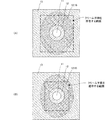
実装基板1には、実装する回路部品毎に、その回路部品のリードを挿入する貫通孔11(スルーホール11)が形成されている。図2、および図3は、このスルーホール部分の拡大図である。図2はクリーム半田を実装面に塗布する前の状態を示しており、図3はクリーム半田を実装面に塗布した後の状態を示している。図2(A)、図3(A)は、実装面の平面図である。図2(B)、図3(B)は、側面断面図である。図2(C)は、裏面(実装面の反対側の面)の平面図である。図2、および図3では、隣接する2つのスルーホール11を示している。スルーホール11の外形は、実装する回路部品のリードの太さよりも、少し大きい。
The mounting
スルーホール11の周囲には、実装する回路部品のリードを半田接続するための金属層12(ランド12)が形成されている。ランド12は、半田付けされた回路部品のリードと電気的に接続される。ランド12は、スルーホール11を通して、実装面から裏面にわたって形成されている。実装面、および裏面におけるランド12の外形は、それぞれ矩形である。また、ここでは、ランド12の面積は、実装面よりも、裏面のほうを大きくしている。
Around the through
なお、図2では、隣接する2つのスルーホール11の周囲に形成したランド12は、つながっていないが、これら2つのスルーホール11に挿入される回路部品のリードを電気的に接続する場合には、これら2つのスルーホール11の周囲に形成したランド12をつなげてもよい。
In FIG. 2, the
また、この実装基板1は、ランド12の外周部を覆うレジスト層13を実装面、および裏面に形成している。図2(A)、(C)、および図3(A)では、形成されている金属層の外形を破線で示している。また、ランド12やレジスト層13形成されている範囲を図示するために、実装基板1の外形を便宜的に示している。ここでは、ランド12、およびレジスト層13が形成されていない領域が存在する実装基板1を例示しているが、このランド12、およびレジスト層13が形成されていない領域は、レジスト層13を形成しておいてもよい。
Further, the mounting
ランド12は、実装面、および裏面において、その大半がレジスト層13に覆われており、スルーホール11の周辺の一部が露出しているだけである。レジスト層13は、ランド12や回路パターン(不図示)が形成されていない領域にも形成されている。例えば、レジスト層13は、図2(B)に示すように、隣接する2つのスルーホール11の周辺に形成されているランド12間にも形成している。実装面、および裏面に形成しているレジスト層13の厚さは、ほぼ均一である。
Most of the
この実装基板1は、図3に示すように、実装面にクリーム半田14を塗布している。クリーム半田14は、露出しているランド12の上だけでなく、スルーホール11の上や、ランド12を覆っているレジスト層13の上にも塗布している。すなわち、実装面において、ランド12が形成されている範囲にクリーム半田14を塗布している。図3(A)では、塗布したクリーム半田14の下方の位置するランド12や、レジスト層13についても、破線で示している。
As shown in FIG. 3, the mounting
なお、クリーム半田14を塗布している領域は、図3(A)ではランド12が形成されている範囲よりも少し大きいが、ランド12が形成されている範囲と同じであってもよいし、また、ランド12が形成されている範囲よりも少し小さくてもよい。また、実装基板1の裏面には、クリーム半田14は塗布されていない。ただし、クリーム半田14を実装面に塗布するときに、その一部がスルーホール11を通って、裏面に達していてもよい。また、図3(B)では、スルーホール11内を半分ほど満たすようにクリーム半田14を塗布した例を示しているが、スルーホール11内全体を満たすようにクリーム半田14を塗布してもよい。
The area where the
このように、この実装基板1は、スルーホール11の周囲に形成しているランド12の外周部を覆うように、レジスト層13を形成している。また、ランド12は、隣接する別のスルーホール11の周囲に形成されているランド12とつながらない大きさであればよい。このため、スルーホール11の周辺に形成するランド12の外形については大きくなるが、回路部品の実装効率については、実質的に低下させることはない。ただし、隣接する2つのスルーホール11に挿入される回路部品のリードを電気的に接続する場合には、これら2つのスルーホール11の周囲に形成したランド12がつながっていてもよい。さらに、クリーム半田14は、露出しているランド12の上だけでなく、ランド12を覆っているレジスト層13の上にも塗布されている。
Thus, the mounting
次に、この実装基板1に対して、回路部品を実装する工法について説明する。回路部品の実装は、リフロー工法により行われる。図4、および図5は、回路部品を実装する工程を説明する図である。図4(A)は、クリーム半田が塗布されていない状態であり、図4(B)に示すように、実装基板1に対してクリーム半田14を塗布する。そして、実装する回路部品を実装基板1に載置する。具体的には、実装する回路部品毎に、その回路部品のリードを対応するスルーホール11に実装面側から挿入する(図4(C)参照)。
Next, a method for mounting circuit components on the mounting
回路部品を載置した実装基板1を、加熱炉に入れる。加熱炉に入れた実装基板1は、熱伝導率が高いランド12に直接塗布されているクリーム半田14が十分に加熱されて溶融し、スルーホール11に流入する(図5(A)参照)。また、時間的に少し遅れて、ランド12を覆っているレジスト層13に塗布しているクリーム半田14が、この覆っているランド12から伝わる熱によって十分に加熱されて溶融する。ランド12を覆っているレジスト層13に塗布していたクリーム半田14は、先にスルーホール11への流入を開始しているクリーム半田14(ランド12に直接塗布されていたクリーム半田14)に引っ張られ、スルーホール11に流入する(図5(B)参照)。
The mounting
実装面には、実装するコネクタ5、抵抗6、コンデンサ7等の回路部品が載置される。このため、実装基板1では、実装面側のほうが、加えられる熱量に生じるロスが大きい。この実装基板1は、上述したように、ランド12の面積を実装面よりも裏面のほうを大きくしている。すなわち、実装基板1の裏面側からの熱を効率的に利用し、レジスト層13に塗布しているクリーム半田14を溶融することができる。
Circuit components such as a
その後、実装基板1が加熱炉から取り出されると、溶融しているクリーム半田14は温度が下がり、周辺の金属(ランド12や回路部品のリード)、およびスルーホール内に付着して固まる(図5(C)参照)。これにより、回路部品のリードがスルーホール11にハンダ付けされる。すなわち、回路部品が、実装基板1に実装される。
After that, when the mounting
このように、回路部品の実装面において、レジスト層13をランド12の外周部を覆うように形成したので、このランド12を覆っているレジスト層13の上に塗布したクリーム半田を十分に加熱し、溶融することができる。したがって、リードが太いコネクタ等の回路部品であっても、半田不足による接続不良が生じるのを抑えられる。また、ランド12は、実装面、および裏面において露出している部分が抑えられるので、リフロー工法によってランド12に付着する余分な半田が抑えられる。すなわち、回路部品の実装に必用な半田の量が抑えられる。さらに、裏面側においても、スルーホール11の周辺にランド12、およびこのランド12の外周部を覆うレジスト層13を形成しているので、溶融したクリーム半田14が裏面まで流れても、裏面側のランド12全体に広がるのを防止できる。
Thus, since the resist
また、実装面や裏面に形成するランド12の外形形状は、矩形に限らず、図6に示す楕円であってもよいし、図7に示す真円であってもよい。また、クリームハンド14を塗布する領域は、図6(A)や図7(A)に示すように、ランド12に外接する矩形形状としてもよいし、図6(B)や図7(B)に示すように、角部がランド12に内接する矩形形状としてもよい。さらには、ランド12と同じ楕円や真円としてもよい。また、クリーム半田14を塗布する領域は、ランド12を形成している領域よりも少し小さくしたり、少し大きくしたりしてもよい。
Further, the outer shape of the
また、隣接する2つのスルーホール11のランド12間におけるレジスト層13の厚さは、図8(A)に示すように、ランド12の厚さと、このランド12を覆っているレジスト層13の厚さと、の和と同じ厚さにしてもよいし、図8(B)に示すように、少し厚くしてもよい。このようにすれば、リフロー工法で溶けた半田によって、隣接する2つのスルーホール11が短絡するのを一層確実に防止できる。
Further, as shown in FIG. 8A, the thickness of the resist
1−実装基板
11−スルーホール(貫通孔)
12−ランド(金属層)
13−レジスト層
14−クリーム半田
1-Mounting board 11-Through hole (through hole)
12-land (metal layer)
13-resist layer 14-cream solder
Claims (7)
前記回路部品の実装面側には、前記貫通孔の周辺に金属層、およびこの金属層の外周部を覆うレジスト層が形成されており、
さらに、前記レジスト層に覆われていない前記金属層の上だけでなく、前記金属層を覆っている前記レジスト層の上にも、半田を塗布した、実装基板。 In a mounting board that has a plurality of through holes into which leads of circuit components to be mounted are inserted,
On the mounting surface side of the circuit component, a metal layer is formed around the through hole, and a resist layer covering the outer peripheral portion of the metal layer is formed,
Furthermore, the mounting board | substrate which apply | coated the solder not only on the said metal layer not covered with the said resist layer but on the said resist layer covering the said metal layer.
前記裏面側も、前記貫通孔の周辺に金属層を形成している、請求項1に記載の実装基板。 The metal layer is formed continuously from the mounting surface to the back surface that is the opposite surface through the through hole,
The mounting substrate according to claim 1, wherein a metal layer is also formed around the through hole on the back surface side.
この実装基板に実装する回路部品毎に、その回路部品のリードを対応する前記貫通孔に挿入して、前記実装基板に載置し、
実装する回路部品を載置した前記実装基板を加熱炉に入れ、前記実装基板に載置している回路部品をリフロー工法で半田付けする、実装方法。 A mounting method for mounting a circuit component on the mounting board according to claim 1,
For each circuit component to be mounted on this mounting substrate, insert the lead of the circuit component into the corresponding through hole, and place it on the mounting substrate.
A mounting method in which the mounting substrate on which the circuit component to be mounted is placed is placed in a heating furnace, and the circuit component placed on the mounting substrate is soldered by a reflow method.
Priority Applications (1)
| Application Number | Priority Date | Filing Date | Title |
|---|---|---|---|
| JP2008247158A JP2010080667A (en) | 2008-09-26 | 2008-09-26 | Mounting board and mounting method |
Applications Claiming Priority (1)
| Application Number | Priority Date | Filing Date | Title |
|---|---|---|---|
| JP2008247158A JP2010080667A (en) | 2008-09-26 | 2008-09-26 | Mounting board and mounting method |
Publications (1)
| Publication Number | Publication Date |
|---|---|
| JP2010080667A true JP2010080667A (en) | 2010-04-08 |
Family
ID=42210782
Family Applications (1)
| Application Number | Title | Priority Date | Filing Date |
|---|---|---|---|
| JP2008247158A Pending JP2010080667A (en) | 2008-09-26 | 2008-09-26 | Mounting board and mounting method |
Country Status (1)
| Country | Link |
|---|---|
| JP (1) | JP2010080667A (en) |
Cited By (3)
| Publication number | Priority date | Publication date | Assignee | Title |
|---|---|---|---|---|
| JP2013162103A (en) * | 2012-02-08 | 2013-08-19 | Juki Corp | Electronic component mounting method, electronic component mounting device, and electronic component mounting system |
| JP2013162102A (en) * | 2012-02-08 | 2013-08-19 | Juki Corp | Electronic component mounting device, electronic component mounting system and electronic component mounting method |
| JP2013179190A (en) * | 2012-02-08 | 2013-09-09 | Juki Corp | Device, system and method for mounting electronic component |
Citations (4)
| Publication number | Priority date | Publication date | Assignee | Title |
|---|---|---|---|---|
| JPH05259622A (en) * | 1992-03-16 | 1993-10-08 | Matsushita Electric Ind Co Ltd | Printed wiring board |
| JP2002026497A (en) * | 2000-07-04 | 2002-01-25 | Hitachi Media Electoronics Co Ltd | Printed wiring |
| JP2004071661A (en) * | 2002-08-02 | 2004-03-04 | Hitachi Ltd | Printed circuit board |
| JP2007173687A (en) * | 2005-12-26 | 2007-07-05 | Mitsubishi Electric Corp | Electronic component mounting printed wiring board |
-
2008
- 2008-09-26 JP JP2008247158A patent/JP2010080667A/en active Pending
Patent Citations (4)
| Publication number | Priority date | Publication date | Assignee | Title |
|---|---|---|---|---|
| JPH05259622A (en) * | 1992-03-16 | 1993-10-08 | Matsushita Electric Ind Co Ltd | Printed wiring board |
| JP2002026497A (en) * | 2000-07-04 | 2002-01-25 | Hitachi Media Electoronics Co Ltd | Printed wiring |
| JP2004071661A (en) * | 2002-08-02 | 2004-03-04 | Hitachi Ltd | Printed circuit board |
| JP2007173687A (en) * | 2005-12-26 | 2007-07-05 | Mitsubishi Electric Corp | Electronic component mounting printed wiring board |
Cited By (3)
| Publication number | Priority date | Publication date | Assignee | Title |
|---|---|---|---|---|
| JP2013162103A (en) * | 2012-02-08 | 2013-08-19 | Juki Corp | Electronic component mounting method, electronic component mounting device, and electronic component mounting system |
| JP2013162102A (en) * | 2012-02-08 | 2013-08-19 | Juki Corp | Electronic component mounting device, electronic component mounting system and electronic component mounting method |
| JP2013179190A (en) * | 2012-02-08 | 2013-09-09 | Juki Corp | Device, system and method for mounting electronic component |
Similar Documents
| Publication | Publication Date | Title |
|---|---|---|
| JP5142119B2 (en) | Method of manufacturing printed circuit board having heat dissipation structure and heat dissipation structure of printed circuit board manufactured by the method | |
| JP2009212124A (en) | Printed-circuit board, method of forming frame ground of printed-circuit board, and electronic apparatus | |
| JP2008041995A (en) | Printed wiring board and manufacturing method of printed wiring board | |
| JP2010080667A (en) | Mounting board and mounting method | |
| JP2001156488A (en) | Electronic component with shield case and its manufacturing method | |
| JP4274264B2 (en) | Module manufacturing method | |
| JP2016178150A (en) | Printed board and mounting method | |
| JP4952904B2 (en) | Printed wiring board and motor control apparatus provided with the same | |
| JP2008205101A (en) | Manufacturing method of electronic component mounted substrate and electronic component mounted substrate | |
| JP4863851B2 (en) | Printed board | |
| JP2011135111A (en) | Method for forming frame ground of printed circuit board | |
| JP2008066344A (en) | Multilayer board, and printing method of metal bonding material | |
| JP2005129927A (en) | Joining material stencil | |
| JP4838277B2 (en) | Wiring board structure of electronic component mounting board and electronic component mounting structure | |
| JP2007266510A (en) | Printed wiring board and electric apparatus | |
| JP2008091557A (en) | Electronic component mounting method and apparatus | |
| JP4919932B2 (en) | Printed board | |
| JP2007299816A (en) | Electronic component mounting board and method of manufacturing same | |
| JP2007311428A (en) | Plating method, and mask plate | |
| JP2018107381A (en) | Printed circuit assembly and manufacturing method thereof | |
| JP2009076632A (en) | Part-mounting section structure of printed-circuit board, and manufacturing method therefor | |
| JP2005033042A (en) | Printed board | |
| JP2013004570A (en) | Solder application method | |
| JP2010267679A (en) | Method of connecting printed circuit board with case | |
| JP2006261573A (en) | Mounting method of surface mount components |
Legal Events
| Date | Code | Title | Description |
|---|---|---|---|
| A711 | Notification of change in applicant |
Free format text: JAPANESE INTERMEDIATE CODE: A712 Effective date: 20100802 |
|
| A621 | Written request for application examination |
Free format text: JAPANESE INTERMEDIATE CODE: A621 Effective date: 20110331 |
|
| A977 | Report on retrieval |
Free format text: JAPANESE INTERMEDIATE CODE: A971007 Effective date: 20120427 |
|
| A131 | Notification of reasons for refusal |
Free format text: JAPANESE INTERMEDIATE CODE: A131 Effective date: 20120508 |
|
| A02 | Decision of refusal |
Free format text: JAPANESE INTERMEDIATE CODE: A02 Effective date: 20120911 |