JP2010072076A - Optical multi-level modulation signal generator - Google Patents
Optical multi-level modulation signal generator Download PDFInfo
- Publication number
- JP2010072076A JP2010072076A JP2008236614A JP2008236614A JP2010072076A JP 2010072076 A JP2010072076 A JP 2010072076A JP 2008236614 A JP2008236614 A JP 2008236614A JP 2008236614 A JP2008236614 A JP 2008236614A JP 2010072076 A JP2010072076 A JP 2010072076A
- Authority
- JP
- Japan
- Prior art keywords
- optical
- polarization
- component
- signal
- input
- Prior art date
- Legal status (The legal status is an assumption and is not a legal conclusion. Google has not performed a legal analysis and makes no representation as to the accuracy of the status listed.)
- Granted
Links
Images


Classifications
-
- H—ELECTRICITY
- H04—ELECTRIC COMMUNICATION TECHNIQUE
- H04B—TRANSMISSION
- H04B10/00—Transmission systems employing electromagnetic waves other than radio-waves, e.g. infrared, visible or ultraviolet light, or employing corpuscular radiation, e.g. quantum communication
- H04B10/50—Transmitters
- H04B10/516—Details of coding or modulation
- H04B10/548—Phase or frequency modulation
- H04B10/556—Digital modulation, e.g. differential phase shift keying [DPSK] or frequency shift keying [FSK]
- H04B10/5561—Digital phase modulation
-
- G—PHYSICS
- G02—OPTICS
- G02F—OPTICAL DEVICES OR ARRANGEMENTS FOR THE CONTROL OF LIGHT BY MODIFICATION OF THE OPTICAL PROPERTIES OF THE MEDIA OF THE ELEMENTS INVOLVED THEREIN; NON-LINEAR OPTICS; FREQUENCY-CHANGING OF LIGHT; OPTICAL LOGIC ELEMENTS; OPTICAL ANALOGUE/DIGITAL CONVERTERS
- G02F1/00—Devices or arrangements for the control of the intensity, colour, phase, polarisation or direction of light arriving from an independent light source, e.g. switching, gating or modulating; Non-linear optics
- G02F1/35—Non-linear optics
- G02F1/3515—All-optical modulation, gating, switching, e.g. control of a light beam by another light beam
- G02F1/3517—All-optical modulation, gating, switching, e.g. control of a light beam by another light beam using an interferometer
- G02F1/3519—All-optical modulation, gating, switching, e.g. control of a light beam by another light beam using an interferometer of Sagnac type, i.e. nonlinear optical loop mirror [NOLM]
-
- G—PHYSICS
- G02—OPTICS
- G02F—OPTICAL DEVICES OR ARRANGEMENTS FOR THE CONTROL OF LIGHT BY MODIFICATION OF THE OPTICAL PROPERTIES OF THE MEDIA OF THE ELEMENTS INVOLVED THEREIN; NON-LINEAR OPTICS; FREQUENCY-CHANGING OF LIGHT; OPTICAL LOGIC ELEMENTS; OPTICAL ANALOGUE/DIGITAL CONVERTERS
- G02F1/00—Devices or arrangements for the control of the intensity, colour, phase, polarisation or direction of light arriving from an independent light source, e.g. switching, gating or modulating; Non-linear optics
- G02F1/01—Devices or arrangements for the control of the intensity, colour, phase, polarisation or direction of light arriving from an independent light source, e.g. switching, gating or modulating; Non-linear optics for the control of the intensity, phase, polarisation or colour
- G02F1/09—Devices or arrangements for the control of the intensity, colour, phase, polarisation or direction of light arriving from an independent light source, e.g. switching, gating or modulating; Non-linear optics for the control of the intensity, phase, polarisation or colour based on magneto-optical elements, e.g. exhibiting Faraday effect
-
- G—PHYSICS
- G02—OPTICS
- G02F—OPTICAL DEVICES OR ARRANGEMENTS FOR THE CONTROL OF LIGHT BY MODIFICATION OF THE OPTICAL PROPERTIES OF THE MEDIA OF THE ELEMENTS INVOLVED THEREIN; NON-LINEAR OPTICS; FREQUENCY-CHANGING OF LIGHT; OPTICAL LOGIC ELEMENTS; OPTICAL ANALOGUE/DIGITAL CONVERTERS
- G02F2/00—Demodulating light; Transferring the modulation of modulated light; Frequency-changing of light
- G02F2/004—Transferring the modulation of modulated light, i.e. transferring the information from one optical carrier of a first wavelength to a second optical carrier of a second wavelength, e.g. all-optical wavelength converter
- G02F2/006—All-optical wavelength conversion
Abstract
Description
本発明は光多値変調信号発生装置に関し、例えば、長距離大容量光ファイバ通信等に利用される多値変調方式による光信号を、制御光によって被制御光を光信号化することで発生する装置に適用し得る。 The present invention relates to an optical multi-level modulation signal generator, for example, an optical signal generated by a multi-level modulation method used for long-distance large-capacity optical fiber communication or the like by generating controlled light as an optical signal using control light. Applicable to the device.
インターネットの普及などに伴い、光ファイバ通信の通信容量の大容量化並びに長距離化への要求は近年ますます高まってきている。近年の光ファイバ通信の通信容量の大容量化は、送受信可能な波長チャンネル数を増やすこと(波長多重通信、WDM:Wave length Division Multiplexing)、及び、各波長チャンネル当たりの通信速度を高速化することの両面から進められてきた。 With the spread of the Internet and the like, demands for increasing the communication capacity of optical fiber communication and increasing the distance have been increasing in recent years. Increasing the communication capacity of optical fiber communication in recent years has increased the number of wavelength channels that can be transmitted and received (wavelength multiplex communication, WDM: Wave length Division Multiplexing), and increased the communication speed for each wavelength channel. Has been promoted from both sides.
一方、光ファイバ通信の更なる大容量化・長距離化の一手段として、近年、多値変調方式が注目を集めている。この多値変調方式は、従来、移動体通信方式などで用いられてきた方式であるが、近年、この技術を光ファイバ通信方式に応用しようとの試みが各所でなされている。 On the other hand, in recent years, a multi-level modulation method has attracted attention as a means for further increasing the capacity and the distance of optical fiber communications. This multi-level modulation method has been conventionally used in a mobile communication method or the like, but in recent years, attempts have been made to apply this technique to an optical fiber communication method.
多値変調方式の代表的な方式は、QPSK(Quadrature Phase Shift Keying)フォーマットと呼ばれる方式である。QPSK方式は、一つのタイムスロットに対して、位相が、0を基準として、π/2ラジアン、πラジアン、3/2πラジアンだけ変移した信号を割り当てる通信方式であり、一度に2ビット(4値)の信号を送ることが可能な通信方式である。従来、実用化若しくは実用化が検討されてきた主たる光通信方式の一つは、一つのタイムスロットに対して、信号強度が弱い「0」信号、若しくは、信号強度が強い「1」信号を割り当てる、いわゆるASK(Amplitude Shift Keying)方式若しくはOOK(On−Off Keying)方式であり、実用化若しくは実用化が検討されてきた主たる光通信方式の他の一つは、位相が0若しくはπラジアンの光信号を割り当てるBinary PSK方式(以下、BPSK方式と呼ぶ)であり、いずれも、一つのタイムスロットに対して、2値のデジタル変調値を割り当てる通信方式であった。 A typical multi-level modulation method is a method called a QPSK (Quadrature Phase Shift Keying) format. The QPSK method is a communication method in which a signal whose phase is shifted by π / 2 radians, π radians, and 3 / 2π radians with respect to one time slot as a reference is assigned 2 bits at a time (four values). ) Signal. Conventionally, one of the main optical communication systems that have been studied for practical use or practical use assigns a “0” signal having a low signal strength or a “1” signal having a high signal strength to one time slot. The so-called ASK (Amplitude Shift Keying) method or OOK (On-Off Keying) method is one of the main optical communication methods that have been studied for practical use or practical use. This is a binary PSK system (hereinafter referred to as a BPSK system) in which signals are allocated, and both are communication systems in which binary digital modulation values are allocated to one time slot.
QPSK方式を光ファイバ通信に応用した場合、以下のようなメリットがある。 When the QPSK method is applied to optical fiber communication, there are the following merits.
すなわち、QPSK方式を、従来のOOK方式やBPSK方式と比較した場合、その占有する周波数帯域は同一ながら、QPSK方式は2倍の量のデータを送ることができる。すなわち、通信容量を大容量化でき、周波数利用効率を向上できるというメリットがある。また、このことは逆に言えば、同じデータ容量のOOK方式やBPSK方式と比較して、QPSK方式は半分の占有周波数帯域しか有さないため、WDM方式との併用を考えた場合、より波長チャンネル間隔を狭めることができ、その結果、通信容量を大容量化でき、周波数利用効率を向上できるというメリットをさらに享受することができる。さらにまた、占有する周波数帯域が狭いということは、信号伝送路である光ファイバの有する群速度分散による波形歪みの影響を受け難いことを意味し、すなわち、長距離化の点でもメリットがある。 That is, when the QPSK method is compared with the conventional OOK method or BPSK method, the QPSK method can send twice as much data while the occupied frequency band is the same. That is, there is an advantage that the communication capacity can be increased and the frequency utilization efficiency can be improved. In other words, the QPSK method has only half the occupied frequency band compared to the OOK method and the BPSK method having the same data capacity. The channel interval can be narrowed, and as a result, the communication capacity can be increased and the merit that the frequency utilization efficiency can be improved can be further enjoyed. Furthermore, the fact that the occupied frequency band is narrow means that it is difficult to be affected by the waveform distortion due to the group velocity dispersion of the optical fiber that is the signal transmission line, that is, there is a merit in terms of increasing the distance.
以上のようなQPSK光信号を発生するQPSK光信号発生装置として従来検討が進められてきたのは、主として、非特許文献1に示すような、電気変調信号を光変調信号に変換して光信号を発生させる、いわゆるE/O型光変調器をベースとした装置であった。
As a QPSK optical signal generating device that generates the QPSK optical signal as described above, the conventional investigation has been made mainly by converting an electric modulation signal into an optical modulation signal as shown in Non-Patent
非特許文献1においては、LiNbO3結晶におけるポッケルス効果を利用した、マッハツェンダ干渉計型LiNbO3変調器を用いたQPSK光変調器について述べられている。非特許文献1の記載技術では、MZA及びMZBで示される2台のマッハツェンダ干渉計型LiNbO3変調器を用いて、それぞれ40GbpsのBPSK信号を発生し、その後、MZCで示される光カプラを用いてこれらのBPSK信号を合波することで、80GbpsのQPSK信号を発生させている。
Non-Patent
非特許文献1などに示されるE/O型光変調器をベースとしたQPSK光信号発生装置において、その発生し得るQPSK信号のデータビットレートは、E/O型光変調器の動作速度によって制限される。その高速化のためには、電気変調信号を発生する電子デバイス、並びに、E/O型光変調器自体の電気−光変換の高速化が必要である。その動作速度は、現状の市販品の技術レベルとしては50Gbps程度のビットレートが現状の限界である。すなわち、QPSK信号のデータレートとしては100Gbps程度が限界である。
In a QPSK optical signal generator based on an E / O type optical modulator shown in Non-Patent
電子デバイス並びにE/O型光変調器の動作速度限界を超えて、さらに高速のQPSK信号を発生するには、制御信号となる光変調信号を用いて被制御光信号である信号光を変調する、全光学信号制御技術をベースとした、全光型光変調器を利用することが望ましい。 In order to generate a higher-speed QPSK signal that exceeds the operating speed limit of the electronic device and the E / O type optical modulator, the signal light that is the controlled optical signal is modulated using the optical modulation signal that becomes the control signal. It is desirable to use an all-optical light modulator based on all-optical signal control technology.
光ファイバにおいて発現する光カー効果を利用する方法は、その好ましい一例である。光ファイバにおいて発現する光カー効果は、光ファイバを強度の強い光が伝播することにより光ファイバの屈折率が変化する現象であり、その応答速度は数フェムト秒(fs)である。 A method using the optical Kerr effect developed in an optical fiber is a preferred example. The optical Kerr effect that appears in an optical fiber is a phenomenon in which the refractive index of the optical fiber changes due to the propagation of strong light through the optical fiber, and the response speed is several femtoseconds (fs).
上記で述べたような、光ファイバ中での光カー効果を利用して、超高速光スイッチを作成した例が、例えば、非特許文献2に開示の方法などで実現されている。非特許文献2の記載技術において、光カー効果を発現させる光ファイバとして偏波保存単一モード光ファイバ(以下、「偏波面保存光ファイバ」(あるいは単に「光ファイバ」)と呼ぶ)が利用されている。偏波面保存光ファイバは、このファイバの光の伝播方向(以後「光ファイバの光軸方向」ということもある)に対して垂直な面内に設定された遅相軸あるいはスロー(slow)軸と呼ばれる光学軸の方向と、slow軸と直交する進相軸あるいはファスト(fast)軸と呼ばれる光学軸の方向とでは、導波される光に対する等価屈折率が異なる構造のものである。
An example in which an ultrafast optical switch is created using the optical Kerr effect in an optical fiber as described above is realized by the method disclosed in Non-Patent
そして、非特許文献2に開示されている光スイッチに利用されている光ファイバは、2本の偏波保存単一モード光ファイバの光学軸を直交させて融着された面を有し、偏波面保存型の単一モード光ファイバの有する複屈折性を相殺できる構造を有している。この光スイッチには、偏波面保存光ファイバの光学軸と平行な偏波面を有する直線偏波の制御光と、偏波面保存光ファイバの光学軸から45°傾いた偏波面を有する直線偏波の信号光(被制御光)が入力される。なお、この明細書において、「偏波」を「偏光」と同意語として用いている。
The optical fiber used in the optical switch disclosed in Non-Patent
この光スイッチに信号光を構成する光パルスのみが入力された場合には、信号光の光パルスは、この光スイッチへの入力時と同一の直線偏波状態で出力される。一方、信号光と共に制御光の光パルスが、信号光の光パルスと同期して入力された場合には、信号光の光パルスの偏波成分のうち制御光の光パルスの偏波方向と平行な偏波成分に対して、制御光の光パルスによって光カー効果が誘起される。すなわち、光カー効果によって、信号光の光パルスと制御光の光パルスとの間で発現する相互位相変調効果によって、信号光の光パルスに位相シフトが生じる。 When only the optical pulse constituting the signal light is input to the optical switch, the optical pulse of the signal light is output in the same linear polarization state as that when input to the optical switch. On the other hand, when the optical pulse of the control light is input together with the signal light in synchronization with the optical pulse of the signal light, the polarization component of the optical pulse of the signal light is parallel to the polarization direction of the control light optical pulse. The optical Kerr effect is induced by the optical pulse of the control light with respect to a simple polarization component. That is, the optical Kerr effect causes a phase shift in the optical pulse of the signal light due to the cross-phase modulation effect that appears between the optical pulse of the signal light and the optical pulse of the control light.
この位相シフト量φがπに等しいとき、信号光の光パルスの偏波方向が、この光スイッチへの入力時に対して90°回転する。すなわち、信号光の光パルスの偏波方向が、光ファイバの光学軸に対して−45°の方向になる。光スイッチの出力側に検光子を配置することで、制御光により信号光の光パルスを通過させたり、遮断したりすることができる。すなわち、検光子の光学軸の方向を、信号光の光パルスの偏波方向がこの光スイッチへの入力時に対して90°回転している場合には透過し、入力時と同一の偏波方向である場合には遮断する向きに設定して配置すれば、制御光によって偏波面が回転された光パルスのみがこの光スイッチを透過できるので、制御光によって、信号光の光パルスをスイッチできる。 When the phase shift amount φ is equal to π, the polarization direction of the optical pulse of the signal light is rotated by 90 ° with respect to the input time to the optical switch. That is, the polarization direction of the optical pulse of the signal light is −45 ° with respect to the optical axis of the optical fiber. By arranging the analyzer on the output side of the optical switch, the optical pulse of the signal light can be passed or blocked by the control light. That is, the direction of the optical axis of the analyzer is transmitted when the polarization direction of the optical pulse of the signal light is rotated by 90 ° with respect to the input to the optical switch, and the same polarization direction as that at the input In such a case, if it is arranged in the blocking direction, only the optical pulse whose polarization plane is rotated by the control light can pass through this optical switch, so that the optical pulse of the signal light can be switched by the control light.
非特許文献2に開示の技術で用いられているように、光ファイバ中の光カー効果に基づく相互位相変調効果を用いれば、OOK若しくはASK信号とした制御光の信号パターンを、被制御光である信号光に光位相変調パターンという形で転化できる。すなわち、光ファイバの光カー効果を利用することで、数百ギガビット毎秒(Gbit/s)以上のビットレートで動作する全光型BPSK変調器を実現できることが、上述した従来技術から容易に類推できる。
As used in the technique disclosed in Non-Patent
上記の方式で発生されたBPSK信号を、非特許文献1におけるMZCのような光カプラで合波することで、QPSK光信号を発生することは原理的には可能であることが容易に類推できる。
しかしながら、二つの光BPSK信号を合波してQPSK光信号を発生する際には、光BPSK信号間の光位相差を精密に制御する必要がある。例えば、二つの光BPSK信号がそれぞれ<0>、<π>と位相変調された信号である場合、その間に精密にπ/2の光位相差を与えて合波しなければ、理想的なQPSK信号とはならない。 However, when the two optical BPSK signals are combined to generate a QPSK optical signal, it is necessary to precisely control the optical phase difference between the optical BPSK signals. For example, if two optical BPSK signals are signals that have been phase-modulated with <0> and <π>, respectively, an ideal QPSK unless an optical phase difference of π / 2 is precisely given between them and combined. It is not a signal.
個々の光BPSK信号の光位相は、非特許文献1の場合には電気変調信号によって与えた光位相に加えて、若しくは、上述した光ファイバの光カー効果に基づく方式の場合には光変調信号によって与えられた光位相に加えて、その光信号が経過してきた光経路の光路長によって決まる光位相シフトによって決定される。
The optical phase of each optical BPSK signal is added to the optical phase given by the electrical modulation signal in the case of
一方、非特許文献2に示すような光ファイバを用いた全光学的な位相変調の場合、用いる光ファイバのファイバ長は、実用的な制御光強度でもって十分な光変調効果を得るための相互作用長を確保するために、数十mから数kmという長さが必要となる。すなわち、光波長の数十万倍以上の長さとなる。そのような長尺な光ファイバを伝播してくる光信号の光位相を正確に制御するのは非常に困難である。また、実現するには、精密で、かつ十分な応答速度を有する高価な制御機能が必要となる。さらに加えて、環境温度の変化などにより光ファイバの屈折率が変化すると、光位相も変化してしまうため、その補償までを含めた、複雑で高価な制御機能が必要となる。
On the other hand, in the case of all-optical phase modulation using an optical fiber as shown in Non-Patent
以上のような状況を鑑みたとき、非特許文献2に開示の技術で発生させた光BPSK信号を二つ用意して、これを非特許文献1におけるMZCのような光カプラで合波することで、QPSK光信号を発生する方式は、現実的な実用レベルで考えた場合、非常に実現が困難である。若しくは、実現のためには高精度で、従って高価かつ複雑な光位相制御回路が必要となる。
In view of the above situation, two optical BPSK signals generated by the technique disclosed in
本発明は、以上の点に鑑みなされたものであり、複雑で高精度な制御技術を不要としながら、動作安定に、超高速光多値変調信号を発生可能な、全光型の光多値変調信号発生装置を提供することを目的とする。 The present invention has been made in view of the above points, and is an all-optical optical multi-value capable of generating an ultra-high-speed optical multi-value modulation signal stably without requiring a complicated and high-precision control technique. An object of the present invention is to provide a modulation signal generator.
本発明の光多値変調信号発生装置は、(1)偏波面保存の閉ループ光路を形成させている閉ループ光路部と、(2)ピーク強度の揃った光パルスが等時間間隔に並んだ光パルス列である直線偏波の信号光を2つの直線偏波の第1成分及び第2成分に分ける2成分分割部と、(3)上記閉ループ光路への入出力を行うものであって、上記第1成分及び第2成分を、巡回方向が逆になるように上記閉ループ光路部へ入力する閉ループ入出力部と、(4)信号の「0」及び「1」の並びに応じた強度パターンを有する、上記信号光とは異なる波長を有する直線偏波の第1の制御光信号に応じ、上記第1成分の光位相を変化させる、上記閉ループ光路に介在されている第1成分光位相変調部と、(5)信号の「0」及び「1」の並びに応じた強度パターンを有する、上記第1の制御光信号と同じ波長を有する直線偏波の第2の制御光信号に応じ、上記第2成分の光位相を変化させる、上記閉ループ光路に介在されている第2成分光位相変調部と、(6)上記閉ループ入出力部へ向かう信号光と、上記閉ループ入出力部から出力された戻り光の上記第1成分及び第2成分との光路を分離する正逆光路分離部と、(7)上記信号光の第1成分及び第2成分が進行するいずれかの箇所に設けられ、上記第1成分及び第2成分に相対的な光位相差を付与する光位相差付与部とを備え、(8)上記閉ループ光路以外の光路にも偏波面保存光路を適用すると共に、上記正逆光路分離部から出力された、戻り光の上記第1成分及び第2成分の組、若しくは、戻り光の上記第1成分及び第2成分の少なくとも一方の所定の光学操作を施した後の上記第1成分及び第2成分の組を、多値変調光信号として出力することを特徴とする。 An optical multilevel modulation signal generator according to the present invention includes (1) a closed-loop optical path section that forms a polarization-preserving closed-loop optical path, and (2) an optical pulse train in which optical pulses with uniform peak intensities are arranged at equal time intervals. A two-component splitting unit for dividing the linearly polarized signal light into two linearly polarized first and second components; and (3) input / output to the closed loop optical path, A closed-loop input / output unit that inputs the component and the second component to the closed-loop optical path unit so that the circulation direction is reversed; and (4) an intensity pattern corresponding to the sequence of “0” and “1” of the signal, A first component optical phase modulation unit interposed in the closed loop optical path for changing the optical phase of the first component in response to a linearly polarized first control optical signal having a wavelength different from that of the signal light; 5) Intensity pattern corresponding to "0" and "1" of the signal A second optical signal having the same wavelength as the first control optical signal and having the same wavelength as that of the first control optical signal, the second component being interposed in the closed-loop optical path that changes the optical phase of the second component according to the second control optical signal. A component light phase modulator; (6) a forward / reverse optical path that separates the optical path of the signal light traveling toward the closed-loop input / output unit and the first component and the second component of the return light output from the closed-loop input / output unit; A separation unit; and (7) an optical phase difference that is provided at any location where the first component and the second component of the signal light travel and gives a relative optical phase difference to the first component and the second component. (8) A polarization plane preserving optical path is applied to an optical path other than the closed-loop optical path, and a set of the first component and the second component of the return light output from the forward / reverse optical path separating unit Or at least one of the first component and the second component of the return light. Square of the predetermined pairs of said first and second components after applying the optical operation, and outputs multi-valued modulation optical signal.
ここで、閉ループ光路は、上記第1の制御光信号若しくは上記第2の制御光信号による光カー効果により、上記閉ループ光路を巡回する上記第1成分若しくは上記第2成分に対して相互位相変調効果による位相シフトを生じさせる位相シフト用非線形光ファイバ(例えば、実施形態での第3偏波面保存光ファイバが該当する)を含むと共に、上記位相シフト用非線形光ファイバに上記第1の制御光信号を挿入する第1光カプラ、と、上記位相シフト用非線形光ファイバに上記第1の制御光信号を挿入する第2光カプラとを有し、上記位相シフト用非線形光ファイバと上記第1光カプラとで上記第1成分光位相変調部を構成すると共に、上記位相シフト用非線形光ファイバと上記第2光カプラとで上記第2成分光位相変調部を構成することが好ましい。 Here, the closed-loop optical path has a cross-phase modulation effect on the first component or the second component that circulates the closed-loop optical path due to the optical Kerr effect by the first control optical signal or the second control optical signal. Including a phase shift nonlinear optical fiber (for example, corresponding to the third polarization plane preserving optical fiber in the embodiment) and causing the first control optical signal to be transmitted to the phase shift nonlinear optical fiber. A first optical coupler to be inserted; and a second optical coupler to insert the first control optical signal into the phase shift nonlinear optical fiber, the phase shift nonlinear optical fiber, and the first optical coupler; It is preferable that the first component optical phase modulation unit is configured by the above-described configuration, and that the second component optical phase modulation unit is configured by the phase shift nonlinear optical fiber and the second optical coupler. Arbitrariness.
また、閉ループ入出力部は、偏光ビームスプリッタ又は偏光プリズムでなる、上記2成分分割部を兼ねたものであり、上記閉ループ光路部は、上記第1成分及び上記第2成分の偏波面を90°だけ回転させるループ内偏波面変換部を含むことが好ましい。 The closed-loop input / output unit also serves as the two-component splitting unit formed of a polarizing beam splitter or a polarizing prism, and the closed-loop optical path unit has 90 ° polarization planes of the first component and the second component. It is preferable to include an in-loop polarization plane conversion unit that rotates only by the amount of rotation.
本発明によれば、複雑で高精度な制御技術を不要としながら、動作安定に、超高速光多値変調信号を発生可能な、全光型の光多値変調信号発生装置を提供することができる。 According to the present invention, it is possible to provide an all-optical optical multilevel modulation signal generator capable of generating an ultrafast optical multilevel modulation signal stably without requiring a complicated and highly accurate control technique. it can.
(A)第1の実施形態
以下、本発明による光多値変調信号発生装置の第1の実施形態を、図面を参照しながら説明する。第1の実施形態の光多値変調信号発生装置は、例えば、QPSK光信号を発生する全光型の発生装置に適用できる。
(A) First Embodiment Hereinafter, a first embodiment of an optical multilevel modulation signal generator according to the present invention will be described with reference to the drawings. The optical multilevel modulation signal generator of the first embodiment can be applied to, for example, an all-optical generator that generates a QPSK optical signal.
(A−1)第1の実施形態の構成
図1は、第1の実施形態に係る光多値変調信号発生装置(例えば、全光型のQPSK光信号発生装置)の構成を示す配置図である。
(A-1) Configuration of First Embodiment FIG. 1 is a layout diagram showing a configuration of an optical multilevel modulation signal generator (for example, an all-optical QPSK optical signal generator) according to the first embodiment. is there.
第1の実施形態に係る光多値変調信号発生装置1は、第1偏波分離合成モジュール10と、第2偏波分離合成モジュール18と、第1偏波面保存光ファイバ12と、第2偏波面保存光ファイバ16と、第1偏波面変換部14と、第3偏波面保存光ファイバ22と、第4偏波面保存光ファイバ26と、第2偏波面変換部24と、第1光位相バイアス回路40とを具える。
The optical multilevel
第1偏波分離合成モジュール10は、信号光を入力するための入力用光ファイバ32−2の一端が結合されている第1入出力端10−1と、第1入出力端10−1に対向する側に位置する、第1偏波面保存光ファイバ12の一端が結合されている第2入出力端10−2と、変調された信号光(以下、変調光信号と呼ぶ)を出力する第3入出力端10−3とを具えている。なお、各図において、「入出力端」を「ポート」と表現していることもある。
The first polarization separation /
第2偏波分離合成モジュール18は、第2偏波面保存光ファイバ16の一端を結合する第1入出力端18−1と、第1入出力端18−1に対向する側に位置する、第3偏波面保存光ファイバ22の一端を結合する第2入出力端18−2と、第4偏波面保存光ファイバ26の一端を結合する第3入出力端18−3と、第3入出力端18−3に対向する側に偏波クロストーク成分を出力する第4入出力端18−4を具えている。
The second polarization separation /
なお、第4入出力端18−4は、そこからの光の入出力を行うことはないので、例えば光ファイバピグテール、光コネクタなどの光信号の入出力インターフェイスのための光部品を接続する必要はない。第1の実施形態において、第4入出力端18−4は、後述するように、第3偏波面保存光ファイバ22において生じる偏波クロストークの除去が如何になされるかを説明するために、専ら便宜上設けているだけのものであり、それ自体は第1の実施形態の必須の構成要素ではない。
Since the fourth input / output terminal 18-4 does not input / output light from there, it is necessary to connect optical components for optical signal input / output interfaces such as optical fiber pigtails and optical connectors, for example. There is no. In the first embodiment, the fourth input / output terminal 18-4, as will be described later, in order to explain how the polarization crosstalk generated in the third polarization-maintaining
第1偏波面保存光ファイバ12は、第1偏波分離合成モジュール10の第2入出力端10−2に一端が結合されており、第2偏波面保存光ファイバ16は、第2偏波分離合成モジュール18の第1入出力端18−1に一端が結合されており、第1偏波面保存光ファイバ12の他端と第2偏波面保存光ファイバ16の他端とは第1偏波面変換部14(図1では、Aと示されている位置に設定されている)を介して接続されている。
One end of the first polarization-maintaining
また、第3偏波面保存光ファイバ22は、波長λpの制御光による光カー効果により、波長λsの被制御光である信号光に対して相互位相変調効果による位相シフトを生じさせる、いわゆる非線形光ファイバである。第3偏波面保存光ファイバ22は、第2偏波分離合成モジュール18の第2入出力端18−2に一端が結合されている。第3偏波面保存光ファイバ22は、第1の制御光入力ポート31を有する第1光カプラ20と、第2の制御光入力ポート33を有する第2光カプラ21とを具えている。第1光カプラ20を介して、第1の制御光信号が第3偏波面保存光ファイバ22に入力される。また、第2光カプラ21を介して、第2の制御光信号が第3偏波面保存光ファイバ22に入力される。その際、第1の制御光信号と第2の制御光信号とは、第3偏波面保存光ファイバ22中を互いに逆行して伝播するように、第1光カプラ20及び第2光カプラ21の接続方法が設定されている。
The third polarization-maintaining
第4偏波面保存光ファイバ26は、第2偏波分離合成モジュール18の第3入出力端18−3に一端が結合されており、第3偏波面保存光ファイバ22の他端と第4偏波面保存光ファイバ26の他端とは、第2偏波面変換部24(図1ではBと示されている位置に設定されている)を介して接続されている。
The fourth polarization-maintaining
第3偏波面保存光ファイバ22に具えられた第1光カプラ20及び第2光カプラ21もまた、偏波面保存型の光カプラを用いることが望ましい。直線偏波(直線偏光)である第1の制御光信号は、第1光カプラ20を介して、第3偏波面保存光ファイバ22に導入され、第3偏波面保存光ファイバ22、第4偏波面保存光ファイバ26、第2偏波分離合成モジュール18の順に経由する形で、第3偏波面保存光ファイバ22、第4偏波面保存光ファイバ26などを伝播していく。また、同様に直線偏波である第2の制御光信号は、第2光カプラ21を介して、第3偏波面保存光ファイバ22に導入され、第3偏波面保存光ファイバ22、第2偏波分離合成モジュール18の順に経由する形で、すなわち、第1の制御光信号とは逆行する形で、第3偏波面保存光ファイバ22、第2偏波分離合成モジュール18などを伝播していく。
It is desirable that the first
また、直線偏波である第1及び第2の制御光信号は、第3偏波面保存光ファイバ22中を互いに逆行しつつも、同じ偏波方向で伝播していくものとする。また、それはともに、第3偏波面保存光ファイバ22中を互いに逆行して伝播していく、後述する二つの信号光(S1成分、S2成分)の偏波方向とも合致している。例えば、後述する二つの信号光(S1成分、S2成分)の偏波方向は共に、第3偏波面保存光ファイバ22のslow軸に平行であり、そのような偏波面を有する後述する二つの信号光(S1成分、S2成分)が、直線偏波として第3偏波面保存光ファイバ22中を伝播していく。
Further, it is assumed that the first and second control optical signals that are linearly polarized waves propagate in the same polarization direction while going backward in the third polarization-maintaining
第1〜第4偏波面保存光ファイバ12、16、22、26や、第1、第2光カプラ20、21に利用して好適な偏波面保存光ファイバとしては、パンダ型光ファイバが代表的である。このパンダ型光ファイバは、コアの近傍に応力付与部を形成し、コアに強い応力を加えることにより偏波保持性を得ている。
Panda-type optical fibers are typical examples of polarization-maintaining optical fibers suitable for use in the first to fourth polarization-maintaining
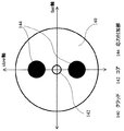
図2は、パンダ型光ファイバの光の伝播方向に対して垂直に切断した断面の概略的構造を示す断面図である。 FIG. 2 is a cross-sectional view showing a schematic structure of a cross section cut perpendicularly to the light propagation direction of the panda optical fiber.
光が導波されるコア142を取り囲むクラッド140に、コア142を挟む形で2つの応力付与部144が形成されている。例えば、クラッド140はSiO2、コア142はGeO2がドープされたSiO2で形成され、応力付与部144はB2O3がドープされたSiO2から形成される。
Two
このように形成することによって、図2中で、パンダ型光ファイバの光の伝播方向に対して垂直な面内に設定されたslow軸との方向と、slow軸と直交するfast軸の方向では、コア142を導波される光に対する等価屈折率が異なる。すなわち、コア142の近くにクラッド140の屈折率より高い屈折率を有する応力付与部144がおかれているために、光の電場ベクトルの振動方向がslow軸の方向に平行な光に対する等価屈折率が、光の電場ベクトルの振動方向がfast軸の方向に平行な光に対する等価屈折率よりも高くなる。このような等価屈折率の非対称性があるために、パンダ型光ファイバに入力される光の偏波面は保存されて伝播されるようになる。
By forming in this way, in FIG. 2, in the direction of the slow axis set in the plane perpendicular to the light propagation direction of the panda optical fiber and the direction of the fast axis orthogonal to the slow axis, The equivalent refractive index for light guided through the
すなわち、パンダ型光ファイバでは、直線偏波の偏波面を、図2に示すslow軸(若しくはfast軸)に合わせて入力すると、偏波状態が保たれたままパンダ型光ファイバ中を伝播し、出射端においても、偏波面が、slow軸(若しくはfast軸)に一致した直線偏波の光成分のみを得ることが可能である。 That is, in the panda type optical fiber, when the polarization plane of linear polarization is input in accordance with the slow axis (or the fast axis) shown in FIG. 2, it propagates in the panda type optical fiber while maintaining the polarization state. Even at the emission end, it is possible to obtain only a linearly polarized light component whose polarization plane coincides with the slow axis (or fast axis).
以下の説明において、便宜のために、第1偏波分離合成モジュール10、第2偏波分離合成モジュール18等の偏波分離合成モジュールへ光が入射する場合、入射光の偏波分離合成モジュールの偏波面選択反射面に対する電場ベクトルの振動方向に対応する成分を次のように定義する。すなわち、偏波面選択反射面へ入射する入射光の入射面に平行な方向に電場ベクトルが振動する成分をp成分(p偏波成分、p波とも呼ぶ)、入射光の入射面に垂直な方向に電場ベクトルが振動する成分をs成分(s偏波成分、s波とも呼ぶ)と呼ぶこととする。
In the following description, for the sake of convenience, when light enters the polarization separation / combination module such as the first polarization separation /
例えば、第1偏波分離合成モジュール10へ光が入射する場合、第1偏波分離合成モジュールを構成している偏波分離合成素子の偏波面選択反射面10Rに対する入射面に平行な方向に電場ベクトルが振動する成分はp成分、入射光の入射面に垂直な方向に電場ベクトルが振動する成分はs成分である。第2偏波分離合成モジュール18においても同様である。
For example, when light is incident on the first polarization separation /
第1偏波分離合成モジュール10においては、第1入出力端10−1から入力されたp偏波成分は、第2入出力端10−2に出力され、第2入出力端10−2から入力されたs偏波成分は、第3入出力端10−3に出力される。また、第2入出力端10−2から入力されたp偏波成分は、第1入出力端10−1に出力される。なお、この第1の実施形態の場合、第1偏波分離合成モジュール10の第1入出力端10−1からs偏波成分が入力されることはない。
In the first polarization separation /
第1偏波分離合成モジュール10等の偏波分離合成モジュールには、例えば市販されている偏光ビームスプリッタの中から好適なものを選んで利用することができる。あるいはまた、上記の説明で想定している薄膜を用いたタイプの偏光ビームスプリッタに限定されず、複屈折結晶を用いたいわゆる偏光プリズムを用いたものであっても良い。
As the polarization separation / combination module such as the first polarization separation /
また、第1偏波分離合成モジュール10、第2偏波分離合成モジュール18等の偏波分離合成モジュールの各入出力端と、それと結合する第1〜第4偏波面保存光ファイバ12、16、22、26等の偏波面保存光ファイバの入出力端とは、偏波分離合成モジュールのp波ないしはs波の偏波方向と、偏波面保存光ファイバのslow軸ないしfast軸の方向とが合致するように接合されているものとする。以下の説明では、便宜のために、各偏波分離合成モジュールのp波の偏波方向と、各偏波面保存光ファイバのslow軸の方向とが合致するように接合されているものとして説明する。但し、第1の実施形態及び後述する各実施形態は、この結合形態には限定されず、何箇所かの接合個所が、偏波分離合成モジュールのp波の偏波方向と、偏波面保存光ファイバのfast軸の方向とが合致するように接合されていたとしても良く、後述する各実施形態の効果を発揮させることができる。
Also, each input / output end of the polarization separation / combination module such as the first polarization separation /
第1偏波面保存光ファイバ12における、第1偏波分離合成モジュール10と接続されていない側の他端と、第2偏波面保存光ファイバ16における、第2偏波分離合成モジュール18と接続されていない側の他端とは、第1偏波面変換部14を介して接続される。第1偏波面変換部14は、入力された直線偏波に対して、その偏波方向が45°回転された直線偏波を出力させるものである。
The other end of the first polarization plane preserving
図3は、第1偏波面変換部14の構成例を示す説明図であり、図3では2例を示している。
FIG. 3 is an explanatory diagram showing a configuration example of the first
第1偏波面変換部14は、例えば、図3(A)に示すように、第1偏波面保存光ファイバ12及び第2偏波面保存光ファイバ16の互いに対面する他端の端面74、76において、互いのslow軸同士が45°回転される形で融着接続して実現できる。
For example, as shown in FIG. 3A, the first polarization
また例えば、第1偏波面変換部14は、図3(B)に示すように、第1偏波面保存光ファイバ12及び第2偏波面保存光ファイバ16の互いのslow軸同士が一致するようにし、その代わりに、接合部に1/2波長板114を挿入して実現するようにしても良い。1/2波長板114の光軸方向を、互いのslow軸から22.5°回転される形になるように配置することで実現できる。以下では、便宜上、第1偏波面変換部14は、図3(B)に示すような1/2波長板114を利用したものとして説明する。
Further, for example, as shown in FIG. 3B, the first polarization
また、第3偏波面保存光ファイバ22における、第2偏波分離合成モジュール18と接続されていない側の他端と、第4偏波面保存光ファイバ26における、第2偏波分離合成モジュール18と接続されていない側の他端とは、上述したように、第2偏波面変換部24を介して接続される。第2偏波面変換部24は、入力された直線偏波に対して、その偏波方向が90°回転された直線偏波を出力させるものである。このような第2偏波面変換部24は、例えば、図4に示すように、第3偏波面保存光ファイバ22及び第4偏波面保存光ファイバ26の互いに対面する他端の端面174、176において、互いのslow軸同士が90°回転される形で融着接続されることで実現できる、言い換えれば、一方のslow軸と他方のfast軸が平行になるように融着接続することで実現することができる。また例えば、第2偏波面変換部24は、図示は省略するが、第1偏波面変換部14の場合と同様に、互いのslow軸同士が一致するようにし、その代わりに、接合部に、その光軸方向が互いのslow軸から45°回転された1/2波長板を挿入することで実現するようにしても良い。
In addition, the other end of the third polarization plane preserving
ここで、第1偏波分離合成モジュール10の第2入出力端10−2から第1偏波面変換部14に至る経路の長さ、すなわち第1偏波面保存光ファイバ12の長さをl1(経路L1ということもある)、第1偏波面変換部14から第2偏波分離合成モジュール18の第1入出力端18−1に至る経路の長さ、すなわち第2偏波面保存光ファイバ16の長さをl2(経路L2ということもある)、第2偏波分離合成モジュール18の第2入出力端18−2から第2偏波面変換部24に至る経路、すなわち第3偏波面保存光ファイバ22の長さをl3(経路L3ということもある)、第2偏波面変換部24から第2偏波分離合成モジュール18の第3入出力端18−3に至る経路、すなわち第4偏波面保存光ファイバ26の長さをl4(経路L4ということもある)とする。
Here, the length of the path from the second input / output terminal 10-2 of the first polarization separation /
なお、光カー効果の発現による位相シフトの発生に特段の寄与をしない、第1偏波面保存光ファイバ12、第2偏波面保存光ファイバ16、第4偏波面保存光ファイバ26は、光ファイバではなく、空間光学系の経路とするようにしても良く、このようにしても同様な効果を得ることができる。
The first polarization plane preserving
また、第3偏波面保存光ファイバ22に具えられた第1光カプラ20や第2光カプラ21としては、光分岐比が1:1に設計されたいわゆる3dB光カプラや、それぞれ波長の異なる制御光及び信号光を合波・分離するべく設計されたWDMカプラを用いることができる。
The first
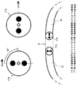
第1光位相バイアス回路40は、第3偏波面保存光ファイバ22若しくは第4偏波面保存光ファイバ26の中途の任意の場所に挿入される(図1では、第4偏波面保存光ファイバ26の中途に挿入されている場合を示している)。図5は、第1光位相バイアス回路40の構成例を示す説明図である。
The first optical
第1光位相バイアス回路40は、例えば、直線偏波の偏波面を+45°だけ回転する第1ファラデー回転子278、直線偏波の偏波面を−45°だけ回転する第2ファラデー回転子280、光軸X、Yを有する第1の1/4波長板282を有する。図5においては、便宜上、第1光位相バイアス回路40は、第4偏波面保存光ファイバ26の中途に挿入されているが、上述のように挿入箇所はここに限定されるものではない。第1の1/4波長板282の光軸方向は後述するように設定されている。
The first optical
今、図中右側の第4偏波面保存光ファイバ26の左端276から、第4偏波面保存光ファイバ26のfast軸方向に平行な直線偏波が出力され、第1光位相バイアス回路40に入射されたとする(図5では、このときの入射光をS1成分と記載している)。この場合、まず、第2ファラデー回転子280を通過して、偏波方向が−45°だけ回転される。偏波回転された直線偏波の偏波方向が、その光軸方向の一つ(図5では、Y軸)と一致するように、第1の1/4波長板282が配置されている。この光は、第1の1/4波長板282を、そのY軸と平行な直線偏波として通過した後、第1ファラデー回転子278に入力される。そして、第1ファラデー回転子278において、偏波方向が+45°だけ回転される。そして、この光は、その偏波方向が図中左側の第4偏波面保存光ファイバ26のfast軸に平行な直線偏波として、図中左側の第4偏波面保存光ファイバ26の右端274に結合(入射)され、再び第4偏波面保存光ファイバ26を伝播していく。
Now, linear polarization parallel to the fast axis direction of the fourth polarization-maintaining
一方、図中左側の第4偏波面保存光ファイバ26の右端274から、第4偏波面保存光ファイバ26のfast軸方向に平行な直線偏波が出力され、第1光位相バイアス回路40に入射されたとする(図5では、このときの入射光をS2成分と記載している)。この場合、この光は、まず、第1ファラデー回転子278を通過して、偏波方向が+45°だけ回転される。このとき、偏波回転された直線偏波の偏波方向は、第1の1/4波長板282のX軸方向と一致する。この光は、第1の1/4波長板282を、そのX軸と平行な直線偏波として通過した後、第2ファラデー回転子280に入力される。そして、第2ファラデー回転子280において、偏波方向が−45°だけ回転される。この光は、その偏波方向が図中右側の第4偏波面保存光ファイバ26のfast軸に平行な直線偏波として、図中右側の第4偏波面保存光ファイバ26の左端276に結合(入射)され、再び第4偏波面保存光ファイバ26を伝播していく。
On the other hand, a linearly polarized wave parallel to the fast axis direction of the fourth polarization plane preserving
第1の実施形態の光多値変調信号発生装置1は、以上の構成を有するが、この光多値変調信号発生装置1の周辺構成要素として、第1光サーキュレータ30、2つの光バンドパスフィルタ28及び38が設けられている。
The optical multilevel
第1光サーキュレータ30は、第1入出力端30−1に接続されている入力用光ファイバ32−2から入力された信号光を、第2入出力端30−2に接続されている入力用光ファイバ32−2に出力して、第1偏波分離合成モジュール10の第1入出力端10−1に入射させるものである。また、第1光サーキュレータ30は、第1偏波分離合成モジュール10の第1入出力端10−1から出力され、入力用光ファイバ32−2を介して第2入出力端30−2に入力された光を、第3入出力端30−3に接続されている出力用光ファイバ37に出力するものである。
The first
光バンドパスフィルタ38は、第1光サーキュレータ30の第3入出力端30−3から出力用光ファイバ37に出力された光の所定帯域(中心波長は信号光の波長λsと一致している)だけを濾波し、言い換えると、波長λpの制御光成分などを遮断し、出力用光ファイバ39に出力するものである。
The optical band-
光バンドパスフィルタ28は、第1偏波分離合成モジュール10の第3入出力端10−3から出力用光ファイバ27に出力された光の所定帯域(中心波長は信号光の波長λsと一致している)だけを濾波し、言い換えると、波長λpの制御光成分などを遮断し、出力用光ファイバ29に出力するものである。
The
後述する動作説明で明らかにするように、光バンドパスフィルタ28からの出力光はQPSK光信号であり、光バンドパスフィルタ38からの出力光はQPSK光信号の論理反転信号である。
As will be clarified in the description of the operation described later, the output light from the
(A−2)第1の実施形態の動作
次に、以上のような構成を有する第1の実施形態に係る光多値変調信号発生装置1の動作を説明する。
(A-2) Operation of the First Embodiment Next, the operation of the optical multilevel
波長λsの被制御光である信号光が入力用光ファイバ32−1に入力され、第1光サーキュレータ30及び入力用光ファイバ32−2を経由して、第1偏波分離合成モジュール10の第1入出力端10−1に到達する。
Signal light, which is controlled light having a wavelength λs, is input to the input optical fiber 32-1 and passes through the first
ここで、信号光は、ピーク強度の揃った光パルスが等時間間隔に並んだ、いわゆる光パルス列である。パルス時間間隔は、所望とするQPSK信号のデータビットレートの逆数の2倍と一致する。すなわち、10Gbit/sのデータレートのQPSK光信号を最終的に所望する場合、光パルス列である信号光のパルス時間間隔は200ピコ秒(ps)、繰り返し周波数にして5ギガヘルツ(GHz)である。 Here, the signal light is a so-called optical pulse train in which optical pulses with uniform peak intensities are arranged at equal time intervals. The pulse time interval coincides with twice the reciprocal of the data bit rate of the desired QPSK signal. That is, when a QPSK optical signal having a data rate of 10 Gbit / s is finally desired, the pulse time interval of the signal light as the optical pulse train is 200 picoseconds (ps), and the repetition frequency is 5 gigahertz (GHz).
第1偏波分離合成モジュール10の第1入出力端10−1に到達する信号光は、p偏波成分に平行な直線偏波となるようにその偏波方向が調整されているものとする。その結果、信号光は、第1偏波分離合成モジュール10の第2入出力端10−2から直線偏波として出力される。その後、信号光は、第1偏波面保存光ファイバ12中を、そのslow軸と平行な直線偏波として伝播し、図1中左側の経路から第1偏波面変換部14に至る。
It is assumed that the polarization direction of the signal light reaching the first input / output terminal 10-1 of the first polarization separation /
第1偏波面変換部14への入出力端となる、第1偏波面保存光ファイバ12と第2偏波面保存光ファイバ16の対向するファイバ端面74、76は、上述のように、また、図3(B)に示したように、第1偏波面変換部14に1/2波長板114が挿入されているとした場合、以下のように調整されている。すなわち、互いのslow軸方向が一致するように調整されている。さらにまた、第1偏波面変換部14のいずれか一方の光学軸を、第1偏波面保存光ファイバ12及び第2偏波面保存光ファイバ16のslow軸から、22.5°だけ傾けられている。
As described above, the fiber end faces 74 and 76 of the first polarization plane preserving
図1中左側の経路から第1偏波面変換部14へ入力され、第1偏波面変換部14から出力されて第2偏波面保存光ファイバ16に結合される信号光の偏波方向は、図6(A)に示すように、第2偏波面保存光ファイバ16のslow軸と45°だけ傾いた直線偏波となる。
The polarization direction of the signal light that is input to the first polarization
上述したように、また、図3(A)に示したように、第1偏波面保存光ファイバ12と第2偏波面保存光ファイバ16の互いのファイバ端面を、互いのslow軸方向が相対的に45°回転した状態で融着接続することで、第1偏波面変換部14を構成させても良い。このような融着接続を用いた場合には1/2波長板114は不要である。またこのときも、上述の場合と同様に、第2偏波面保存光ファイバ16に結合される信号光の偏波方向は、第2偏波面保存光ファイバ16のslow軸と45°だけ傾いた直線偏波となる(図6(A))。
As described above and as shown in FIG. 3A, the fiber end surfaces of the first polarization plane-maintaining
第1偏波面変換部14として図3に示す2つの構成例のいずれを適用した場合でも、その後、信号光は、第2偏波面保存光ファイバ16中を、そのslow軸と平行な直線偏波成分(以下、S1成分と呼ぶ)と、そのfast軸方向に平行な直線偏波成分(以下、S2成分と呼ぶ)とに分かれて伝播し、第2偏波分離合成モジュール18の第1入出力端18−1に入力される。S1成分とS2成分の強度比は、第2偏波面保存光ファイバ16に結合される、直線偏波たる信号光の偏波方向が、第2偏波面保存光ファイバ16のslow軸に対して45°だけ傾いているため、1:1となる。
Regardless of which of the two configuration examples shown in FIG. 3 is applied as the first polarization
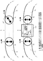
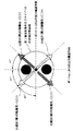
以下では、光信号の偏波方向及び光位相状態を便宜的に表すために、図6(A)〜(E)に示すようなベクトル表記を用いることとする。 In the following, in order to represent the polarization direction and optical phase state of an optical signal for convenience, vector notation as shown in FIGS. 6 (A) to 6 (E) is used.
例えば、信号光が、第1偏波面保存光ファイバ12から第2偏波面保存光ファイバ16へ入力するときの信号光の偏波状態は、図6(A)のように表される。第1偏波面保存光ファイバ12を伝播する信号光は、slow軸に平行な直線偏波で、これを図中上向きの矢印で表している。この信号光が、第1偏波面変換部14から第2偏波面保存光ファイバ16へ入力されるとき、その偏波方向が第2偏波面保存光ファイバ16のslow軸に対して時計方向に45°だけ回転している。従って、S1成分は、このとき図中上向きの矢印、S2成分は、図中右向きの矢印として表される。S1成分及びS2成分の振幅(ベクトルの大きさ)は等しい。また、この段階では、それらの間に相対的な位相差も生じていない。
For example, the polarization state of the signal light when the signal light is input from the first polarization-maintaining
このような信号光(のS1成分及びS2成分)が第2偏波分離合成モジュール18の第1入出力端18−1に入力されると、第2偏波分離合成モジュール18において、S1成分及びS2成分が分岐され、S1成分は入出力端18−2に出力され、S2成分は入出力端18−3に出力される。
When such signal light (the S1 component and S2 component thereof) is input to the first input / output terminal 18-1 of the second polarization separation /
ここで、第1及び第2の制御光信号は、波長がλp、データビットレートが所望とするQPSK信号のデータビットレートの半分であるOOK若しくはASK光信号であるとする。すなわち、10Gbit/sのデータレートのQPSK光信号を最終的に所望する場合、第1及び第2の制御光信号は、ビットレートが5Gbit/sのOOK若しくはASK光信号である。 Here, it is assumed that the first and second control optical signals are OOK or ASK optical signals whose wavelength is λp and whose data bit rate is half the data bit rate of the desired QPSK signal. That is, when a QPSK optical signal having a data rate of 10 Gbit / s is finally desired, the first and second control optical signals are OOK or ASK optical signals having a bit rate of 5 Gbit / s.
第1の制御光信号は、制御光入力ポート31から当該光多値変調信号発生装置1に入力され、第1光カプラ20を経由して、第3偏波面保存光ファイバ22のslow軸に平行な直線偏波になるように、その偏波面が調整されて入力される。また、第1の制御光信号における一つの光パルス信号が、第3偏波面保存光ファイバ22に入力されるときに、信号光のS1成分における一つの光パルスと時間的に一致するように、第1の制御光信号若しくは信号光のタイミングが調整されて入力される。但し、光カー効果を生じさせる第3偏波面保存光ファイバ22において、群速度分散による制御光と信号光間のウォークオフの効果が存在するときには、光カー効果による相互位相変調効果を最大化するために、第1の制御光信号の光パルス位置と信号光(のS1成分)の光パルス位置に若干のオフセットを与えて入力するようにしても良い。
The first control light signal is input from the control
一方、第2の制御光信号は、制御光入力ポート33から当該光多値変調信号発生装置1に入力され、第2光カプラ21を経由して、第3偏波面保存光ファイバ22のslow軸に平行な直線偏波になるように、その偏波面が調整されて入力される。また、第2の制御光信号における一つの光パルス信号が、第3偏波面保存光ファイバ22に入力されるときに、信号光のS2成分における一つの光パルスと時間的に一致するように、第2の制御光信号若しくは信号光のタイミングが調整されて入力される。但し、光カー効果を生じさせる第3偏波面保存光ファイバ22において、群速度分散による制御光と信号光間のウォークオフの効果が存在するときには、光カー効果による相互位相変調効果を最大化するために、第2の制御光信号の光パルス位置と信号光(のS2成分)の光パルス位置に若干のオフセットを与えて入力するようにしても良い。
On the other hand, the second control optical signal is input from the control
以下では、便宜のために、所望する位相変調光信号が、信号「0」が光位相「0」、信号「1」が光位相「π」に対応付けられた位相変調光信号であるとして説明する。 In the following, for convenience, it is assumed that the desired phase-modulated optical signal is a phase-modulated optical signal in which the signal “0” is associated with the optical phase “0” and the signal “1” is associated with the optical phase “π”. To do.
また同様に、便宜のために、ASK光信号である第1又は第2の制御光信号が、信号「1」に対応するピーク強度が1に対して、信号「0」に対応するピーク強度が限りなく0に近い、消光比が無限大の振幅変調信号であるとして説明する。このような振幅変調信号(ASK光信号)は、OOK信号と呼ばれることもある。 Similarly, for convenience, the first or second control optical signal that is an ASK optical signal has a peak intensity corresponding to the signal “1” of 1 and a peak intensity corresponding to the signal “0”. The description will be made assuming that the amplitude modulation signal is infinitely close to 0 and has an infinite extinction ratio. Such an amplitude modulation signal (ASK optical signal) may be called an OOK signal.
第1又は第2の制御光信号が「0」である場合、信号光は何ら相互位相変調による位相シフトを受けない。この状態を、光位相「0」の位相変調信号であるとする。 When the first or second control light signal is “0”, the signal light does not undergo any phase shift due to cross phase modulation. This state is assumed to be a phase modulation signal having an optical phase “0”.
まずはじめに、第1及び第2の制御光信号の入力がない場合を考える。あるいはまた、第1及び第2の制御光信号が「0」であり、信号光は何ら相互位相変調による位相シフトを受けない場合を考える。また、便宜上、当面は、第1光位相バイアス回路40における、後述する光位相バイアス効果を考慮しないで議論を進める。
First, consider a case where there is no input of the first and second control light signals. Alternatively, consider a case where the first and second control light signals are “0” and the signal light does not undergo any phase shift due to cross-phase modulation. For the sake of convenience, the discussion will proceed for the time being without considering the optical phase bias effect described later in the first optical
第1偏波面変換部14から出力された信号光のS1成分は、第2偏波分離合成モジュール18と、第3偏波面保存光ファイバ22と、第2偏波面変換部24と、第1光位相バイアス回路40が設けられた第4偏波面保存光ファイバ26と、第2偏波分離合成モジュール18とで構成される閉ループを巡回した後、第2偏波面保存光ファイバ16を経由し、再度、第1偏波面変換部14に入力される。また、第1偏波面変換部14から出力された信号光のS2成分は、第2偏波分離合成モジュール18と、第1光位相バイアス回路40が設けられた第4偏波面保存光ファイバ26と、第2偏波面変換部24と、第3偏波面保存光ファイバ22と、第2偏波分離合成モジュール18とで構成される閉ループを巡回した後、第2偏波面保存光ファイバ16を経由し、再度、第1偏波面変換部14に入力される。
The S1 component of the signal light output from the first polarization
ここで、第1偏波面変換部14から出力された信号光のS1成分が、上述した光路を介して第1偏波面変換部14に戻ってくるまでの光路長と、第1偏波面変換部14から出力された信号光のS2成分が、上述した光路を介して第1偏波面変換部14に戻ってくるまでの光路長と考える。この光路長の始点及び終点は、第2偏波面保存光ファイバ16の左端、すなわち図6に示す端面76である。ここで、光路長とは、光ファイバなどの光学媒体の物理長に屈折率を掛けた値であり、屈折率が異なる光学媒体が縦続接続されている場合には、各光学媒体毎の光路長の総和である。
Here, the optical path length until the S1 component of the signal light output from the first polarization
S1成分は、まず第2偏波面保存光ファイバ16をそのslow軸方向に平行な直線偏波として伝播し、次に、第3偏波面保存光ファイバ22をそのslow軸方向に平行な直線偏波として伝播する。さらに、第2偏波面変換部24を経由した後、第4偏波面保存光ファイバ26をそのfast軸方向に平行な直線偏波として伝播する。そして、第2偏波面保存光ファイバ16をそのfast軸方向に平行な直線偏波として伝播し、その左端に再度到達する。
The S1 component first propagates through the second polarization-maintaining
従って、このとき、S1成分の経過する全光路長は、(1)式に示すようになる。(1)式においては、各偏波面保存光ファイバのslow軸の屈折率をns、fast軸の屈折率をnfで表している。 Therefore, at this time, the total optical path length in which the S1 component passes is as shown in the equation (1). (1) In the formula, it represents the refractive index of the slow axis of each polarization-maintaining optical fiber n s, a refractive index of fast axis n f.
nsL2+nsL3+nfL4+nfL2 …(1)
一方、S2成分は、まず第2偏波面保存光ファイバ16をそのfast軸方向に平行な直線偏波として伝播し、次に、第4偏波面保存光ファイバ26をそのfast軸方向に平行な直線偏波として伝播する。さらに、第2偏波面変換部24を経由した後、第3偏波面保存光ファイバ22をそのslow軸方向に平行な直線偏波として伝播する。そして、第2偏波面保存光ファイバ16をそのslow軸方向に平行な直線偏波として伝播し、その左端に再度到達する。
n s L2 + n s L3 + n f L4 + n f L2 (1)
On the other hand, the S2 component first propagates through the second polarization plane preserving
従って、S2成分の経過する全光路長は、(2)式に示すようになる。 Therefore, the total optical path length in which the S2 component passes is as shown in the equation (2).
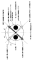
nfL2+nfL4+nsL3+nsL2 …(2)
(1)式及び(2)式から、S1成分及びS2成分は閉ループの巡回方向は逆ではあるが、第2偏波面保存光ファイバ16の左端より入力され、第2偏波面保存光ファイバ16の左端に再度到達するまでの光路長は、全く同じであることが分かる。すなわち、第1及び第2の制御光信号の入力がない、若しくはともに「0」信号である場合、S1成分、S2成分の間には、第2偏波面保存光ファイバ16の左端に再度到達するまでの間に相対的な光位相の差は生じない。従って、第2偏波面保存光ファイバ16の左端に再度到達したときの、S1成分、S2成分のベクトル表現は、図6(B)及び図6(D)に示すようになる。すなわち、図6(A)の場合と同様に、上向きの矢印、右向きの矢印として表現される。但し、再度到達したS1成分の偏波方向はfast軸に平行となり、S2成分の偏波方向はslow軸に平行となるため、図6(A)に示す、第2偏波面保存光ファイバ16の左端入力時の状態に比較して、互いに偏波方向を入れ替えた状態となる。以上のように、第1光位相バイアス回路40における、光位相バイアス効果を考慮しない場合、これらS1成分及びS2成分は同じ光路を通過するので、この段階で相対的な光位相差は生じない。
n f L2 + n f L4 + n s L3 + n s L2 (2)
From Eqs. (1) and (2), the S1 component and S2 component are input from the left end of the second polarization-maintaining
これらのS1成分及びS2成分が、再び、第1偏波面変換部14を逆方向に通過する。その結果、第1偏波面保存光ファイバ12の右端に再度結合するときのS1成分及びS2成分はそれぞれ、第1偏波面保存光ファイバ12のslow軸方向から見て、それぞれ反時計回りに45°(−45°とする)、時計回りに45°(+45°とする)だけ傾いた直線偏波となる。すなわち、ベクトルで表記すれば、図6(B)及び図6(D)に示すように、S1成分は左斜め45°方向の上向きの矢印、S2成分は右斜め45°方向の上向きの矢印として表される。
These S1 component and S2 component pass through the first
次に、第1及び第2の制御光信号が信号「1」である場合を考える。この場合、信号光に対して光カー効果に基づく相互位相変調による位相シフトが生じる。 Next, consider a case where the first and second control light signals are the signal “1”. In this case, a phase shift due to mutual phase modulation based on the optical Kerr effect occurs with respect to the signal light.
制御光信号による相互位相変調による位相シフトの効果は、信号光と同一方向に伝播する制御光信号からの効果と、逆行する制御光信号からの効果の2つの寄与が存在する。すなわち、信号光のS1成分に対しては、同一方向に伝播する第1の制御光信号からの寄与と、逆行する第2の制御光信号からの寄与が存在する。一方、信号光のS2成分に対しては、同一方向に伝播する第2の制御光信号からの寄与と、逆行する第1の制御光信号からの寄与が存在する。 The effect of the phase shift by the mutual phase modulation by the control light signal has two contributions: the effect from the control light signal propagating in the same direction as the signal light and the effect from the reverse control light signal. That is, for the S1 component of the signal light, there is a contribution from the first control light signal propagating in the same direction and a contribution from the reverse second control light signal. On the other hand, for the S2 component of the signal light, there is a contribution from the second control light signal propagating in the same direction and a contribution from the reverse first control light signal.
ここで、第1及び第2の制御光信号の信号「1」のピーク強度を、それによってそれぞれ同一方向に伝播するS1成分又はS2成分に対する相互位相変調による位相シフトの総量がπであるように設定する。また、光カー効果を生じさせる第3偏波面保存光ファイバ22が長手方向に対称な構造を有するとする。さらに、第1及び第2の制御光信号が同じデューティ比、同じ波長、同じマーク率の光信号であるとする(このようなことが、実際上、最も多く適用されると考えられる)。
Here, the peak intensity of the signal “1” of the first and second control optical signals is set so that the total amount of phase shift due to cross-phase modulation with respect to the S1 component or S2 component propagating in the same direction is π. Set. Further, it is assumed that the third polarization-maintaining
このような場合、πシフトに必要な第1及び第2の制御光信号の信号「1」のピーク強度は同一であり、また、第1及び第2の制御光信号の平均強度も同一である。 In such a case, the peak intensity of the signal “1” of the first and second control light signals necessary for the π shift is the same, and the average intensity of the first and second control light signals is also the same. .
第3偏波面保存光ファイバ22のファイバ長が、数十m〜数kmの実用的な長さであるとき、逆行する制御光信号からの相互位相変調による位相シフトの効果は、それぞれの信号光パルスに対して同量だけ与えられる時間無依存の連続的な位相シフトとなり、かつ、その量は逆行する制御光信号の平均強度で決定されることが、参考文献1などで明らかにされている。
When the fiber length of the third polarization-maintaining
参考文献1:M.Jinno and T.Matsumoto,“Nonlinear Sagnac interferometer switch and its applications”,IEEE J.Quantum Electron.,Vol.28,No.4,pp.875−882,1992
すなわち、上述したように、第1及び第2の制御光信号が同じデューティ比、同じ波長、同じマーク率の光信号であり、また、第3偏波面保存光ファイバ22のファイバ長が十分長いような、実際上のアプリケーションで多くの場合が生じるような状況においては、S1成分及びS2成分に対する逆行制御光信号による相互位相変調による位相シフトは、同量である。また、この位相シフトは、S1成分及びS2成分を構成する個々の光パルス信号に対して、制御光信号の「1」、「0」にかかわらず常に同量だけ与えられる。
Reference 1: M.M. Jinno and T.J. Matsumoto, “Nonlinear Sagnac interferometer switch and its applications”, IEEE J. MoI. Quantum Electron. , Vol. 28, no. 4, pp. 875-882, 1992
That is, as described above, the first and second control optical signals are optical signals having the same duty ratio, the same wavelength, and the same mark ratio, and the fiber length of the third polarization-maintaining
従って、逆行制御光信号による相互位相変調による位相シフトの効果は、上述した想定状況下においては、S1成分及びS2成分を構成する個々の光パルス信号に対して、全く同量だけ与えられるので、これを位相シフトとして考慮する必要がない。すなわち、相互位相変調による位相シフトは、同一方向に伝播する制御光信号(S1成分の場合、第1の制御光信号であり、S2成分の場合、第2の制御光信号)からの寄与のみを考慮すれば良い。 Therefore, since the effect of the phase shift due to the cross-phase modulation by the retrograde control optical signal is given to the individual optical pulse signals constituting the S1 component and the S2 component in exactly the same amount under the assumed situation described above, There is no need to consider this as a phase shift. In other words, the phase shift due to the mutual phase modulation only contributes from the control light signal propagating in the same direction (the first control light signal in the case of the S1 component and the second control light signal in the case of the S2 component). Consider it.
なお、第1及び第2の制御光信号が、同じデューティ比、同じ波長、同じマーク率の光信号ではなく、従って、逆行制御光信号による相互位相変調による位相シフトの効果がS1成分及びS2成分に対して同量でないような場合においても、後述する第1光位相バイアス回路40において与える光位相バイアス量を適宜調整することで、その位相シフトの効果の相違を相殺することができる。
Note that the first and second control optical signals are not optical signals having the same duty ratio, the same wavelength, and the same mark ratio. Therefore, the effect of phase shift due to cross-phase modulation by the retrograde control optical signal is the S1 component and the S2 component. Even when the amount is not the same, the difference in the effect of the phase shift can be offset by appropriately adjusting the amount of optical phase bias applied in the first optical
S1成分及びS2成分それぞれに対して、それらと同一方向に伝播する第1及び第2の制御光信号によって、π位相シフトが与えられた場合の、第2偏波面保存光ファイバ16の左端に再度到達したときの、S1成分及びS2成分のベクトル表現は、図6(C)及び図6(E)に示すようになる。すなわち、位相が反転するために、S1成分は左向きの矢印、S2成分は下向きの矢印として表される。 When the π phase shift is given to the S1 component and the S2 component, respectively, by the first and second control optical signals propagating in the same direction as the S1 component and the S2 component again, The vector representations of the S1 component and the S2 component when they reach are as shown in FIGS. 6 (C) and 6 (E). That is, since the phase is inverted, the S1 component is represented as a left-pointing arrow and the S2 component is represented as a downward-pointing arrow.
これらのS1成分及びS2成分が、再び、第1偏波面変換部14を逆方向に通過した後、第1偏波面保存光ファイバ12の右端に再度結合したときには、S1成分及びS2成分はそれぞれ、図6(C)及び図6(E)に示すように、右斜め45°方向の下向きの矢印、左斜め45°方向の下向きの矢印として表される。
When these S1 component and S2 component again pass through the first polarization
第1偏波面変換部14を通過し、第1偏波面保存光ファイバ12の右端に再度結合された信号光は、第1偏波分離合成モジュール10の第2入出力端10−2に入力される。その後、信号光のs偏波成分のみが第3入出力端10−3から出力される。
The signal light that has passed through the first
第1偏波分離合成モジュール10の第2入出力端10−2に入力されるs偏波成分とは、図6(A)〜(E)に示す第1偏波面保存光ファイバ12の右側の端面74において、そのfast軸と平行な偏波成分を意味する。
The s-polarization component input to the second input / output terminal 10-2 of the first polarization separation /
第1偏波面保存光ファイバ12の左端の断面図と、第1偏波分離合成モジュール10の内部から第3入出力端10−3に出力される偏波方向と、第1偏波面保存光ファイバ12の左端に到達した信号光のS1及びS2成分の偏波状態との関係を、図7に模式的に示している。
Sectional drawing of the left end of the 1st polarization plane preserving
S1成分に着目すると、第1偏波分離合成モジュール10の第3入出力端10−3に出力されるS1成分の光位相は、第1の制御光信号の「1」、「0」に応じて反転する(位相がπだけ変化する)ことが分かる。すなわち、第1偏波分離合成モジュール10の第3入出力端10−3からは、S1成分がOOK信号である第1の制御光信号の強度パターンで位相変調された、BPSK信号が出力されることが分かる。
Focusing on the S1 component, the optical phase of the S1 component output to the third input / output terminal 10-3 of the first polarization separation /
S2成分についても同様で、第1偏波分離合成モジュール10の第3入出力端10−3からは、S2成分がOOK信号である第2の制御光信号の強度パターンで位相変調された、BPSK信号が出力されることが分かる。
The same applies to the S2 component. From the third input / output terminal 10-3 of the first polarization beam splitting / combining
すなわち、第1偏波分離合成モジュール10の第3入出力端10−3からは、第1の制御光信号の強度パターンで位相変調されたBPSK信号と、第2の制御光信号の強度パターンで位相変調されたBPSK信号との二つのBPSK信号が同じ偏波方向で出力される。
That is, from the third input / output terminal 10-3 of the first polarization separation /
次に、これら二つのBPSK信号間の位相差を考える。 Next, consider the phase difference between these two BPSK signals.
上述した理由によって、第1偏波面変換部14を経過し、第1偏波面保存光ファイバ12の右端に再度結合された状態でのS1成分及びS2成分間には、制御光信号による相互位相変調によって生じたπの光位相差しか生じない。これらが、第1偏波面保存光ファイバ12を経過し、第1偏波分離合成モジュール10の第2入出力端10−2に入力され、第3入出力端10−3に出力されるまでに生じる位相変化は、結果として、第1偏波面保存光ファイバ12をそのfast軸に平行な直線偏波として伝播したときの光学長による位相変化であり、これは常に同量である。すなわち、この経路で二つのBPSK信号間に位相差を生じさせることができない。
For the reason described above, the mutual phase modulation by the control optical signal is performed between the S1 component and the S2 component in the state where the first polarization
すなわち、二つのBPSK信号間に位相差は生じない。この状態で生じるのは、位相(0、π)と位相(0、π)を組み合わせた4値の多値変調信号である。 That is, there is no phase difference between the two BPSK signals. What occurs in this state is a quaternary multilevel modulation signal in which the phase (0, π) and the phase (0, π) are combined.
QPSK信号化するには、二つのBPSK信号間にπ/2の位相差を与える必要がある。 In order to make a QPSK signal, it is necessary to give a phase difference of π / 2 between two BPSK signals.
第3偏波面保存光ファイバ22若しくは第4偏波面保存光ファイバ26の中途に、図5に示すような第1光位相バイアス回路40を挿入することで、これら二つのBPSK信号間にπ/2の位相差を与えることができる。
By inserting a first optical
図5を参照して、二つのBPSK信号間にπ/2の位相差を与える動作を説明する。ここでは、第1光位相バイアス回路40が、第4偏波面保存光ファイバ26の中途に挿入されているとする。
With reference to FIG. 5, the operation of giving a phase difference of π / 2 between two BPSK signals will be described. Here, it is assumed that the first optical
まず、S1成分は、上述したように、図中右側の第4偏波面保存光ファイバ26の左端276から、そのfast軸に平行な直線偏波として出力され、第1光位相バイアス回路40に結合(入射)される。第1光位相バイアス回路40において、まず、第2ファラデー回転子280を経過して、偏波方向が−45°だけ回転される。偏波方向が−45°だけ回転されたS1成分の偏波方向が、その光軸方向の一つ(図5では、Y軸)と一致するように、複屈折媒体である第1の1/4波長板282を配置されている。S1成分は、第1の1/4波長板282を、そのY軸と平行な直線偏波として通過した後、第1ファラデー回転子278に入力される。そして、第1ファラデー回転子278において、偏頗方向が+45°だけ回転される。その結果、S1成分は、その偏波方向が図中左側の第4偏波面保存光ファイバ26のfast軸に平行な直線偏波として、図中左側の第4偏波面保存光ファイバ26の右端274に結合され、再び第4偏波面保存光ファイバ26を伝播していく。
First, as described above, the S1 component is output from the
一方、S2成分は、上述したように、図中左側の第4偏波面保存光ファイバ26の右端274から、そのfast軸に平行な直線偏波として出力され、第1光位相バイアス回路40に結合される。第1光位相バイアス回路40にて、まず、第1ファラデー回転子278を経過して、偏波方向が+45°だけ回転される。このとき、偏波方向が+45°だけ回転されたS2成分の偏波方向は、第1の1/4波長板282のX軸と一致する。従って、S2成分は、第1の1/4波長板282を、そのX軸と平行な直線偏波として通過する。その後、第2ファラデー回転子280に入力される。そして、第2ファラデー回転子280において、偏頗方向が−45°だけ回転される。その結果、S2成分は、その偏波方向が図中右側の第4偏波面保存光ファイバ26のfast軸に平行な直線偏波として、図中右側の第4偏波面保存光ファイバ26の左端276に結合され、再び第4偏波面保存光ファイバ26を伝播していく。
On the other hand, as described above, the S2 component is output as a linearly polarized wave parallel to the fast axis from the
すなわち、S1成分及びS2成分は、第1光位相バイアス回路40の挿入にもかかわらず、当該箇所以外は、上述したのと同じ偏波状態で、各光路を通過していく。すなわち、第1光位相バイアス回路40挿入箇所以外での信号光のS1成分及びS2成分の光位相の変化や偏波方向の変化の様相に変化はない。
That is, the S1 component and the S2 component pass through each optical path in the same polarization state as described above except for the portion, regardless of the insertion of the first optical
一方、第1光位相バイアス回路40の挿入によって、S1成分及びS2成分は、第1光位相バイアス回路40内に配置された複屈折媒体である第1の1/4波長板282を、互いに直交する光軸(X軸、Y軸)に平行な直線偏波の状態で通過する。そのため、この両成分間に、複屈折媒体である第1の1/4波長板282の有する複屈折に基づく光位相差が生じる。ここで、複屈折媒体が1/4波長板であるために、その光位相差をπ/2とすることができる。
On the other hand, due to the insertion of the first optical
従って、上述のような第1光位相バイアス回路40を挿入することで、結果的に、第1偏波分離合成モジュール10の第3入出力端10−3に出力されるときの信号光のS1成分、S2成分間にπ/2の位相差を付与して出力することができる。その結果、出力される二つのBPSK信号間の位相組み合わせを、位相(0、π)と位相(π/2、3π/2)とすることができ、すなわち、QPSK信号化することができる。
Therefore, by inserting the first optical
その後、このQPSK光信号は、第1偏波分離合成モジュール10の第3入出力端10−3に結合された出力用光ファイバ27を経由し、光バンドパスフィルタ28に入力される。光バンドパスフィルタ28は、波長λsの信号光の波長成分のみを選択的に通過させ、波長λpの制御光成分を遮断する。光バンドパスフィルタ28を通過した波長λsの光成分は、出力用光ファイバ29に結合され、最終的に所望とされるQPSK光信号が出力される。
Thereafter, the QPSK optical signal is input to the
なお、第1光カプラ20及び第2光カプラ21としてWDMフィルタを用いた場合、第1の制御光信号は、第2光カプラ21を介して第2の制御光入力ポート33に出力され、第2偏波分離合成モジュール18に入力されない。また、第2の制御光信号は第1光カプラ20を介して第1の制御光入力ポート31に出力され、第2偏波分離合成モジュール18に入力されない。従って、この場合、第1偏波分離合成モジュール10の第3入出力端10−3からは制御光信号成分が出力されないため、光バンドパスフィルタ28が不要となり、光バンドパスフィルタ28を省略することができる。
When WDM filters are used as the first
(A−3)第1の実施形態の効果
以上述べたように、第1の実施形態においては、光ファイバ中での超高速な光カー効果に基づく相互位相変調効果を用いて、電子デバイスの速度制限を越えた超高速QPSK光信号を発生することができる。また、装置を構成する主要素である偏波面保存光ファイバの複屈折は、(1)式及び(2)式に示されるように、自動的にキャンセルされる構造を有している。すなわち、複屈折をキャンセルするための偏波面保存光ファイバ長の高精度な調整など、複雑かつ高精度な制御が不要である。言い換えれば、非特許文献1や非特許文献2に開示の技術における、干渉計の光路調整のための格別の制御手段を必要とせずに、より簡便かつ安定な光干渉計の構成が可能となる。
(A-3) Effects of the First Embodiment As described above, in the first embodiment, the cross-phase modulation effect based on the ultrafast optical Kerr effect in the optical fiber is used, and the electronic device An ultra-high speed QPSK optical signal exceeding the speed limit can be generated. Further, the birefringence of the polarization-maintaining optical fiber, which is the main element constituting the apparatus, has a structure that is automatically canceled as shown in the equations (1) and (2). That is, complicated and high-precision control such as high-precision adjustment of the polarization-preserving optical fiber length for canceling birefringence is unnecessary. In other words, it is possible to construct a simpler and more stable optical interferometer without requiring special control means for adjusting the optical path of the interferometer in the techniques disclosed in
さらにまた、第3偏波面保存光ファイバ22及び第4偏波面保存光ファイバ26で生じる偏波クロクトーク成分は、全て第2偏波分離合成モジュール18の、光ファイバ等への結合を必要としない第4入出力端18−4に出力される。従って、第1偏波分離合成モジュール10の第3入出力端10−3に、第3偏波面保存光ファイバ22で生じる偏波クロクトーク成分が、本来所望とするQPSK光信号に混在して出力されることはない。
Furthermore, all of the polarization crosstalk components generated in the third polarization-maintaining
従って、必要な制御光信号のピーク強度を低減するために、長尺な第3偏波面保存光ファイバ22を用いても、それらのファイバで生じる偏波クロストークによる動作不安定性の発現を抑制できる。
Therefore, in order to reduce the required peak intensity of the control optical signal, even if the long third polarization plane preserving
以上のことから、第1の実施形態においては、偏波面保存光ファイバの使用による複屈折の影響や、また、偏波クロストークの発生による、光変調動作の動作不安定性を抑制できる。このことから、信号光波長や環境温度が変化しても特性が変化せず、また、高安定な動作特性を担保した装置を提供することができる。 From the above, in the first embodiment, it is possible to suppress the influence of birefringence due to the use of the polarization-maintaining optical fiber and the operational instability of the light modulation operation due to the occurrence of polarization crosstalk. Therefore, even if the signal light wavelength or the environmental temperature changes, the characteristics do not change, and a device that ensures highly stable operating characteristics can be provided.
なお、以上の説明においては、便宜上、光位相(0、π)で変調されたBPSK信号と、光位相(π/2、3π/2)で変調されたBPSK信号の合波による、光位相(0、π/2、π、3π/2)の4値QPSK信号の発生を想定して説明したが、第1の実施形態で実現できる光信号の信号フォーマットは上記に限定されない。例えば、第2の制御光信号の信号「1」のピーク強度を、相互位相変調効果による位相シフトがπ/3となるように調整すれば、光位相(0、π/3、2π/3、π)の4値PSK信号の発生も可能となる。この際、S1成分とS2成分に対する逆行制御光信号による位相シフトに違いは生じるが、これを加味して、第1光位相バイアス回路40で生じさせる光位相差の調整をすれば良い。その際、第1光位相バイアス回路40に内在させる複屈折媒体として、パピネソレイユ補償板のような、光位相差可変の媒体を用いれば、様々な多値変調フォーマットにフレキシブルに対処できる装置の提供が可能となる。
In the above description, for the sake of convenience, the optical phase (by combining the BPSK signal modulated with the optical phase (0, π) and the BPSK signal modulated with the optical phase (π / 2, 3π / 2) ( Although the description has been made assuming the generation of a quaternary QPSK signal of 0, π / 2, π, 3π / 2), the signal format of the optical signal that can be realized in the first embodiment is not limited to the above. For example, if the peak intensity of the signal “1” of the second control optical signal is adjusted so that the phase shift due to the mutual phase modulation effect is π / 3, the optical phase (0, π / 3, 2π / 3, It is also possible to generate a quaternary PSK signal of π). At this time, there is a difference in the phase shift due to the retrograde control optical signal with respect to the S1 component and the S2 component. However, the optical phase difference generated by the first optical
また、第1の実施形態の装置においては、出力用光ファイバ29から出力される、所望とする光多値変調信号とは論理反転した光多値変調信号が、入力用光ファイバ32−2から、信号光と逆行して伝播する形で、同時に出力される。この論理反転信号を、所望とする正論理光多値変調信号の信号品質モニタ等として使用することもできる。この場合において、入力用光ファイバ32−2の信号光入力端に、第1光サーキュレータ30を接続する。第1光サーキュレータ30は、それぞれの入出力端に接続された光ファイバ32−1、32−2、37を有する。光ファイバ32−1から入力された信号光は、光ファイバ32−2から出力される。光ファイバ32−2の他端は、第1偏波分離合成モジュール10の第1入出力端10−1に接続される。第1偏波分離合成モジュール10の第1入出力端10−1に入力される信号光は、p偏波成分に平行な直線偏波となるように、その偏波方向が調整されているものとする。論理反転した光多値変調信号は、第1偏波分離合成モジュール10の第1入出力端10−1から出力され、光ファイバ32−2に入力され、光ファイバ37から出力される。所望とする正論理光多値変調信号の場合と同様に、制御光除去用の光バンドパスフィルタ38を透過する信号光波長成分のみを、論理反転した光多値変調信号として、出力用光ファイバ39を介して出力させる。
In the apparatus of the first embodiment, an optical multilevel modulation signal output from the output
第1の実施形態の効果を要約すると、以下の通りである。すなわち、光ファイバ中での超高速な光カー効果に基づく相互位相変調効果を用いて、電子デバイスの速度制限を越えた超高速QPSK光信号を発生することができる全光型光多値変調信号発生装置を提供することができる。その際、複雑かつ高精度な光路長調整が不要である。さらにまた、信号光波長や環境温度が変化しても特性が変化しない、高安定な動作特性を担保できる。 The effects of the first embodiment are summarized as follows. That is, an all-optical optical multilevel modulation signal capable of generating an ultrafast QPSK optical signal exceeding the speed limit of an electronic device using a cross-phase modulation effect based on an ultrafast optical Kerr effect in an optical fiber A generator can be provided. At that time, complicated and highly accurate optical path length adjustment is not required. Furthermore, highly stable operating characteristics can be ensured that the characteristics do not change even if the signal light wavelength or the environmental temperature changes.
(B)第2の実施形態
次に、本発明による光多値変調信号発生装置の第2の実施形態を、図面を参照しながら説明する。
(B) Second Embodiment Next, a second embodiment of the optical multilevel modulation signal generator according to the present invention will be described with reference to the drawings.
(B−1)第2の実施形態の構成
図8は、第2の実施形態に係る光多値変調信号発生装置の構成を示す配置図であり、第1の実施形態に係る図1との同一、対応部分には同一符号を付して示している。
(B-1) Configuration of Second Embodiment FIG. 8 is an arrangement diagram showing a configuration of an optical multilevel modulation signal generating device according to the second embodiment, and FIG. 8 is related to FIG. 1 according to the first embodiment. The same and corresponding parts are denoted by the same reference numerals.
図8及び図1の比較から明らかなように、第2の実施形態の光多値変調信号発生装置1Aは、第1の実施形態の光多値変調信号発生装置1より簡素化した構成を有する。主たる構成の違いを述べれば、第1の実施形態における、第1偏波分離合成モジュール10及び第2偏波分離合成モジュール18、第1偏波面変換部14及び第2偏波面変換部24、第1偏波面保存光ファイバ12、第2偏波面保存光ファイバ16、第4偏波面保存光ファイバ26を省略し、新たに、出力分岐比が1:1である、偏波面保存3dBカプラ23を用いて、光カー効果を生じさせる第3偏波面保存光ファイバ22を含んだファイバループを構成している。
As apparent from the comparison between FIG. 8 and FIG. 1, the optical multilevel
偏波面保存3dBカプラ23は、4つの入出力端23−1〜23−4を有する2×2の3dBカプラである。入出力端23−1から入力された光(信号光)は、その偏波方向を維持しながら、光強度比1:1の割合で、入出力端23−2及び23−3に分岐出力される。また、入出力端23−2又は23−3から入力された光は、その偏波方向を維持しながら、光強度比1:1の割合で、入出力端23−1及び23−4に分岐出力される。
The polarization plane preserving 3
信号光入力用ファイバ32−2は、偏波面保存3dBカプラ23の入出力端23−1に結合されている。また、偏波面保存3dBカプラ23の入出力端23−2は、非線形ファイバである第3偏波面保存光ファイバ22と点22−aで接続される。また、偏波面保存3dBカプラ23の入出力端23−3は、非線形ファイバである第3偏波面保存光ファイバ22と点22−bで接続される。第1光位相バイアス回路40は、第3偏波面保存光ファイバ22の中途に挿入されている。
The signal light input fiber 32-2 is coupled to the input / output end 23-1 of the polarization plane preserving 3
接続点22−a、22−bにおいて、偏波面保存3dBカプラ23の入出力端23−2、23−3と、第3偏波面保存光ファイバ22の一端及び他端とは、以下のように接続させる。すなわち、互いのslow軸若しくはfast軸が一致するように接続する。
At the connection points 22-a and 22-b, the input / output ends 23-2 and 23-3 of the polarization plane preserving 3
その他の構成は第1の実施形態とはほぼ同様であるため、ここではその説明を割愛し、動作の理解に必要な範囲のみ、必要に応じて以下で説明する。 Since other configurations are substantially the same as those of the first embodiment, description thereof is omitted here, and only a range necessary for understanding the operation will be described below as necessary.
(B−2)第2の実施形態の動作
次に、第2の実施形態に係る光多値変調信号発生装置1Aの動作を、第1の実施形態と相違する点を中心に説明する。
(B-2) Operation of the Second Embodiment Next, the operation of the optical multilevel
第2の実施形態の光多値変調信号発生装置1Aにおいては、第1の実施形態での信号光のS1成分及びS2成分を、偏波面保存3dBカプラ23を用いて生成する。図9を参照しながら、この動作を説明する。
In the optical multilevel
まず、信号光入力用光ファイバ32−2より、偏波面保存3dBカプラ23の入出力端23−1に信号光を入力する。この際、信号光の偏波状態は、偏波面保存3dBカプラ23の入出力端23−1におけるslow軸方向と一致した直線偏波となるように入力する(図9(A)左側)。
First, signal light is input from the signal light input optical fiber 32-2 to the input / output end 23-1 of the polarization plane preserving 3
偏波面保存3dBカプラ23の入出力端23−2及び23−3から、強度比1:1で分岐された信号光がそれぞれ出力される。それぞれの出力信号光の偏波方向は、入出力端23−2、23−3のslow軸方向に一致した直線偏波として出力される。これらの分岐信号光がそれぞれ、接続点22−a、22−bを介して第3偏波面保存光ファイバ22に入力される際、偏波面保存3dBカプラ23の入出力端23−2、23−3と、第3偏波面保存光ファイバ22とは、互いのslow軸及びfast軸が一致しているために、各分岐信号光は、第3偏波面保存光ファイバ22のslow軸に平行な直線偏波として入力される(図9(A)右側)。
Signal lights branched at an intensity ratio of 1: 1 are output from the input / output terminals 23-2 and 23-3 of the polarization plane preserving 3
偏波面保存3dBカプラ23の入出力端23−2及び23−3から、それぞれ接続点22−a、22−bを介して第3偏波面保存光ファイバ22に入力された分岐信号光はそれぞれ、第1の実施形態におけるS1成分、S2成分に相当する。
The branched signal lights input to the third polarization-maintaining
S1成分は、第3偏波面保存光ファイバ22において、第1の制御光信号による位相シフトを受けた後、接続点22−bに到達し、偏波面保存3dBカプラ23の入出力端23−3に入力される。その際の偏波方向は維持されるので、偏波面保存3dBカプラ23の入出力端23−3のslow軸に平行な方向である。第1の制御光信号の「0」、「1」に応じて、光位相が「0」、「π」と変化するので、偏波面保存3dBカプラ23の入出力端23−3に入力されたときのS1成分のベクトル表記は、図9(B)の右側に示すように、第1の制御光信号の「0」又は「1」に応じた上向き又は下向きの矢印で表される。
The S1 component reaches the connection point 22-b in the third polarization plane preserving
S2成分も同様に、第3偏波面保存光ファイバ22において、第2の制御光信号による位相シフトを受けた後、接続点22−aに到達し、偏波面保存3dBカプラ23の入出力端23−2に入力される。その際の偏波方向は維持されるので、偏波面保存3dBカプラ23の入出力端23−2のslow軸に平行な方向である。第2の制御光信号の「0」、「1」に応じて、光位相が「0」、「π」と変化するので、偏波面保存3dBカプラ23の入出力端23−2に入力されたときのS2成分のベクトル表記は、図9(C)の右側に示すように、第2の制御光信号の「0」又は「1」に応じた上向き又は下向きの矢印で表される。
Similarly, the S2 component is also subjected to a phase shift by the second control optical signal in the third polarization-maintaining
S1成分及びS2成分は共に、閉ループ中を第3偏波面保存光ファイバ22のslow軸に平行な偏波方向で伝播するので、その光路長は同一である。また、それぞれ逆行する制御光信号によって生じる位相シフトは、第1の実施形態と同様に同量となる。
Since both the S1 component and the S2 component propagate in the closed loop in the polarization direction parallel to the slow axis of the third polarization-maintaining
閉ループを経由したS1成分及びS2成分は、それぞれ偏波面保存3dBカプラ23の入出力端23−3、23−2に入力され、それぞれの半分の強度の分岐出力が、入出力端23−4より出力される。入出力端23−4より出力されるS1成分及びS2成分の偏波方向は、入出力端23−4のslow軸方向と平行であり、それぞれ、制御光信号の「0」、「1」に対応して位相が反転する(図9(B)、(C)の左側の図)。
The S1 component and S2 component that have passed through the closed loop are respectively input to the input / output terminals 23-3 and 23-2 of the polarization-preserving 3
以下、入出力端23−4から出力されるS1成分及びS2成分の光位相を考察する。まず、上述したように、閉ループ中での光路長によって生じたり、それぞれ逆行する制御光信号によって生じたりする位相シフトは、S1成分及びS2成分について同量であるので、無視できる。また、2×2の3dBカプラ(偏波面保存3dBカプラ23)の性質として、入出力端23−1より入力されて、入出力端23−2から出力される光と、入出力端23−3から出力される光にはπ/2の位相シフトが生じる(例えば、特開2004−309541号参照)。同様に、入出力端23−2より入力されて入出力端23−4から出力される光と、入出力端23−3より入力されて入出力端23−4から出力される光にはπ/2の位相シフトが生じる。すなわち、この偏波面保存3dBカプラ23の部分でS1成分とS2成分とには、(π/2)×2=πの原理的な位相シフトが生じる。しかしながら、この位相差は、結果として生じる二つのBPSK信号の一方が論理反転するだけなので、実用上問題とはならない。
Hereinafter, the optical phases of the S1 component and S2 component output from the input / output terminal 23-4 will be considered. First, as described above, the phase shift caused by the optical path length in the closed loop or caused by the reverse control light signal is the same for the S1 component and the S2 component, and can be ignored. Further, as a property of the 2 × 2 3 dB coupler (polarization plane preserving 3 dB coupler 23), the light input from the input / output end 23-1 and output from the input / output end 23-2 and the input / output end 23-3 A phase shift of π / 2 occurs in the light output from (see, for example, Japanese Patent Application Laid-Open No. 2004-309541). Similarly, the light input from the input / output terminal 23-2 and output from the input / output terminal 23-4 and the light input from the input / output terminal 23-3 and output from the input / output terminal 23-4 are π. A phase shift of / 2 occurs. In other words, a fundamental phase shift of (π / 2) × 2 = π occurs between the S1 component and the S2 component in the polarization plane preserving 3
結果として、偏波面保存3dBカプラ23の入出力端23−4からは、第1の実施形態と同様に、第1及び第2の制御光信号の強度変調パターンを位相変調パターンに転化させた、二つのBPSK信号が出力される。第1光位相バイアス回路40を無視すれば、それらの間には相対的な光位相差がないため、第1の実施形態と同様、この状態で生じるのは、位相(0、π)と位相(0、π)を組み合わせた4値の多値変調信号である。
As a result, from the input / output end 23-4 of the polarization plane preserving 3
第1の実施形態と同様に、第1光位相バイアス回路40を挿入することで、これら二つのBPSK信号間にπ/2の相対位相差を与えることができ、結果として、QPSK光信号を発生させることができる。
Similar to the first embodiment, by inserting the first optical
(B−3)第2の実施形態の効果
第2の実施形態によれば、第1の実施形態と同様な効果に加えて、以下の効果を奏することができる。すなわち、構成部品数を減少させることができるため、より低コストな装置の提供が可能となる。
(B-3) Effects of Second Embodiment According to the second embodiment, in addition to the same effects as those of the first embodiment, the following effects can be achieved. That is, since the number of components can be reduced, it is possible to provide a lower cost apparatus.
(C)第3の実施形態
次に、本発明による光多値変調信号発生装置の第3の実施形態を、図面を参照しながら説明する。
(C) Third Embodiment Next, a third embodiment of the optical multilevel modulation signal generator according to the present invention will be described with reference to the drawings.
第3の実施形態に係る光多値変調信号発生装置は、第2の実施形態で生じる恐れがある問題点を改善しようとしたものであり、その構成例を図10に示す。なお、図10においては、第2の実施形態に係る図8との同一、対応部分には同一符号を付して示している。 The optical multilevel modulation signal generator according to the third embodiment is intended to improve the problems that may occur in the second embodiment, and FIG. 10 shows a configuration example thereof. In FIG. 10, the same and corresponding parts as those in FIG. 8 according to the second embodiment are denoted by the same reference numerals.
第3の実施形態の光多値変調信号発生装置1Bは、第2の実施形態の構成に加えて、第1偏光子25を有する。第1偏光子25は、偏波面保存3dBカプラ23の入出力端23−4に付加されている。ここで、第1偏光子25が透過させる偏波方向は、偏波面保存3dBカプラ23の入出力端23−4におけるslow軸方向と平行な方向である。その他の構成は、第2の実施形態と同様であるため、その説明を割愛する。
The optical multilevel
次に、第3の実施形態における特徴的な動作を説明する。 Next, characteristic operations in the third embodiment will be described.
第2の実施形態で生じる恐れがある問題点は、長尺な第3偏波面保存光ファイバ22を用いたときに生じる偏波クロストーク成分の問題である。
The problem that may occur in the second embodiment is a problem of the polarization crosstalk component that occurs when the long third polarization-maintaining
偏波面保存光ファイバは、一般的には、完全な偏波保持能力を有するものではなく、その物理長が長くなるとその偏波保持能力は劣化していく。一般に、偏波保持能力の劣化は長さ100mを超えてくると顕著になり、その結果、当初入力した直線偏波の入力光の偏波方向と直交した偏波方向の光出力も発現してしまう。これは偏波クロストークと呼ばれている。 In general, the polarization maintaining optical fiber does not have a complete polarization maintaining capability, and the polarization maintaining capability deteriorates as the physical length increases. In general, the deterioration of the polarization maintaining capability becomes significant when the length exceeds 100 m, and as a result, the light output in the polarization direction orthogonal to the polarization direction of the linearly input light that is initially input is also manifested. End up. This is called polarization crosstalk.
第1の実施形態の動作で詳細に説明したように、本装置で用いる非線形ファイバである第3偏波面保存光ファイバ22の長さは数十m〜数kmに及ぶことが想定される。偏波クロストークが生じると、本発明で用いられるような、光干渉計を元にした光変調器の変調動作の安定性が極端に劣化することが知られている(参考文献2参照)。
As described in detail in the operation of the first embodiment, it is assumed that the length of the third polarization-maintaining
参考文献2:S.Arahira et al.,“Modified NOLM for Stable and Improved 2R Operation at Ultra−High Bit Rates”,IEICE Trans. Commun.,Vol.E89−B,No.12,pp.3296−3305,2006
第2の実施形態において、第3偏波面保存光ファイバ22において、S1成分及びS2成分の偏波クロストーク成分が生じた場合、この偏波クロストーク成分は、本来所望とする信号成分と共に偏波面保存3dBカプラ23の入出力端23−2、23−3へと入力され、入出力端23−4へ出力される。偏波クロストーク成分の光位相はランダムであるため、これらの干渉で得られる合成光波形はランダムに変動し、その結果、偏波面保存3dBカプラ23の入出力端23−4から出力される信号光に、波形変動という動作不安定性を生じさせる。
Reference 2: S.M. Arahira et al. "Modified NOLM for Stable and Improved 2R Operation at Ultra-High Bit Rates", IEICE Trans. Commun. , Vol. E89-B, no. 12, pp. 3296-3305, 2006
In the second embodiment, when polarization crosstalk components of S1 component and S2 component are generated in the third polarization-maintaining
さらにまた、偏波面保存3dBカプラ23での偏波面保存光ファイバ結合部での光軸調整が不十分であると、ここでの偏波クロストークにより、偏波面保存3dBカプラ23の入出力端23−4から出力される信号光は、本来所望とする信号成分と偏波クロストーク成分間での干渉が生じる。偏波クロストーク成分の光位相はランダムであるため、偏波面保存3dBカプラ23の入出力端23−4から出力される信号光の波形変動はさらに著しくなり、その結果、さらなる動作不安定性を生じさせる。
Furthermore, if the optical axis adjustment at the polarization plane preserving optical fiber coupling portion in the polarization plane preserving 3
偏波クロストーク成分は、本来所望とする信号光と偏波直交した成分であるため、偏波分離することでその影響を抑えることができる。 Since the polarization crosstalk component is a component orthogonal to the polarization of the originally desired signal light, the influence can be suppressed by polarization separation.
偏波面保存3dBカプラ23の入出力端23−4に、第1偏光子25を配置し、その透過偏波方向を、本来所望とする信号光成分の偏波方向と平行な、入出力端23−4のslow軸方向に合致させることにより、装置出力に含まれる偏波クロストーク成分を低減することができ、その結果、装置から出力される多値変調光信号の波形変動を抑制することが可能となる。
The
(C−3)第3の実施形態の効果
第3の実施形態によれば、第2の実施形態の効果に加えて、以下の効果を奏することができる。すなわち、長尺な第3偏波面保存光ファイバ22を用いても、そこで生じる偏波クロストーク成分による動作不安定性の影響を抑制でき、その結果、動作安定がより高い装の提供が可能となる。
(C-3) Effects of Third Embodiment According to the third embodiment, the following effects can be achieved in addition to the effects of the second embodiment. That is, even if the long third polarization plane preserving
(D)第4の実施形態
次に、本発明による光多値変調信号発生装置の第4の実施形態を、図面を参照しながら説明する。
(D) Fourth Embodiment Next, a fourth embodiment of the optical multilevel modulation signal generator according to the present invention will be described with reference to the drawings.
(D−1)第4の実施形態の構成
図11は、第4の実施形態に係る光多値変調信号発生装置の構成を示す配置図であり、第1の実施形態に係る図1との同一、対応部分には同一符号を付して示している。
(D-1) Configuration of Fourth Embodiment FIG. 11 is a layout diagram showing a configuration of an optical multilevel modulation signal generating device according to the fourth embodiment, which is different from FIG. 1 according to the first embodiment. The same and corresponding parts are denoted by the same reference numerals.
第4の実施形態の光多値変調信号発生装置1Cは、第1の実施形態の光多値変調信号発生装置1に比較すると、第2光位相バイアス回路41を、第1の実施形態における第1偏波面変換部14に代えて挿入すると共に、第1の実施形態における第1光位相バイアス回路40を省略している。
Compared with the optical multilevel
図12は、第4の実施形態で適用する第2光位相バイアス回路41の構成例を示す説明図である。
FIG. 12 is an explanatory diagram illustrating a configuration example of the second optical
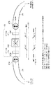
第2光位相バイアス回路41は、直線偏波の偏波面を+22.5°だけ回転する第3ファラデー回転子378、同じく直線偏波の偏波面を+22.5°だけ回転する第4ファラデー回転子380、光軸X、Yを有する第2の1/4波長板382を有する。第2光位相バイアス回路41は、第1偏波面保存光ファイバ12の右端374と第2偏波面保存光ファイバ16の左端376を接続する箇所に挿入される。
The second optical
第2光位相バイアス回路41における光軸方向、偏波方向は、下記のように設定されている。
The optical axis direction and polarization direction in the second optical
今、図中左側の第1偏波面保存光ファイバ12の右端374から、第1偏波面保存光ファイバ12のslow軸方向に平行な直線偏波が出力され、第2光位相バイアス回路41に挿入された場合、まず、第3ファラデー回転子378を経由して、偏波方向が+22.5°だけ回転される。偏波方向が回転された直線偏波の偏波方向が、その光軸方向の一つ(図12では、Y軸)と一致するように、第2の1/4波長板382が配置されている。第3ファラデー回転子378によって偏波方向が+22.5°だけ回転された直線偏波は、第2の1/4波長板382を、そのY軸と平行な直線偏波として通過した後、第4ファラデー回転子380に入力される。そして、第4ファラデー回転子380において、偏波方向が+22.5°だけ回転される。そして、この光は、その偏波方向が図中右側の第2偏波面保存光ファイバ16のslow軸から45°だけ傾いた偏波方向の直線偏波として、図中右側の第2偏波面保存光ファイバ16の左端376に結合され、第2偏波面保存光ファイバ16を伝播していく。
Now, linear polarization parallel to the slow axis direction of the first polarization-maintaining
一方、図中右側の第2偏波面保存光ファイバ16の左端376から、第2偏波面保存光ファイバ16のfast軸方向に平行な直線偏波が出力され、第2光位相バイアス回路41に挿入された場合、この光は、まず、第4ファラデー回転子380を経過して、偏波方向が+22.5°だけ回転される。偏波方向が回転された直線偏波の偏波方向は、第2の1/4波長板382のX軸と一致するように、第2の1/4波長板382が配置されている。第4ファラデー回転子380によって偏波方向が+22.5°だけ回転された直線偏波は、第2の1/4波長板382を、そのX軸と平行な直線偏波として通過した後、第3ファラデー回転子378に入力される。そして、第3ファラデー回転子378において、偏波方向が+22.5°だけ回転される。そして、この光は、その偏波方向が図中左側の第1偏波面保存光ファイバ12のfast軸から45°だけ傾いた偏波方向の直線偏波として、図中左側の第1偏波面保存光ファイバ12の右端374に結合され、第1偏波面保存光ファイバ12を伝播していく。
On the other hand, a linearly polarized wave parallel to the fast axis direction of the second polarization-maintaining
(D−2)第4の実施形態の動作
次に、第4の実施形態における特徴的な動作を説明する。
(D-2) Operation of the Fourth Embodiment Next, a characteristic operation of the fourth embodiment will be described.
第4の実施形態では、第1の実施形態における第1偏波面変換部14と第1光位相バイアス回路40との果たす役割を、一つの第2光位相バイアス回路41でもって代行させている。それによって、必要な光部品の削減による装置作製コストの低減と、装置サイズの小型化が期待できる。
In the fourth embodiment, the role of the first
まず、第2光位相バイアス回路41が、第1の実施形態における第1偏波面変換部14の効果を代行できることを説明する。
First, it will be described that the second optical
今、第1の実施形態と同様に、第1偏波分離合成モジュール10の入出力端10−2を介して、第1偏波面保存光ファイバ12の右端374から、slow軸方向に平行な直線偏波である信号光が出力されたとする。
As in the first embodiment, a straight line parallel to the slow axis direction from the
このとき、第2偏波面保存光ファイバ16の左端376に結合される信号光は、上述したように、第2光位相バイアス回路41を介したことにより、第2偏波面保存光ファイバ16のslow軸から45°だけ傾いた偏波方向の直線偏波となる。
At this time, the signal light coupled to the
これは、第1の実施形態において、第1偏波面変換部14を経過して第2偏波面保存光ファイバ16に結合される信号光の偏波状態と同一である。すなわち、第1偏波面変換部14に代えて、第2光位相バイアス回路41を用いても、同じ効果が実現できる。
This is the same as the polarization state of the signal light that passes through the first
次に、第2光位相バイアス回路41が、第1の実施形態における第1光位相バイアス回路40の機能を代行できることを説明する。
Next, it will be described that the second optical
第2偏波面保存光ファイバ16の左端376から第2光位相バイアス回路41へ入力される、当初の信号光と逆行する進行方向(図12における図中右から左への進行方向)の信号光は、第1の実施形態の動作の項で説明したように、第1光位相バイアス回路40が設けられていない場合には、二つのBPSK信号(S1成分及びS2成分)となっている。ここで、第1の実施形態において説明したように、一方のBPSK信号であるS1成分の偏波方向は、第2偏波面保存光ファイバ16の左端376において、そのfast軸と平行な方向である。また、他方のBPSK信号であるS2成分の偏波方向は、第2偏波面保存光ファイバ16の左端376において、そのslow軸と平行な方向である。また、第1の実施形態において説明したように、第2偏波面保存光ファイバ16の左端376から出力される時点においては、これら二つのBPSK信号(S1成分及びS2成分)は、制御光信号からの相互位相変調効果によって生じる位相シフト以外の光位相差を持たない。
Signal light in the traveling direction (traveling direction from right to left in the drawing in FIG. 12) input to the second optical
S1成分は、第2光位相バイアス回路41を経由し、第1偏波面保存光ファイバ12の右端374に到達するまでに、図12に示すように、偏波方向の状態(偏波面状態)を遷移させる。すなわち、第4ファラデー回転子380で偏波方向を+22.5°だけ回転させた直線偏波となり、その後、第2の1/4波長板382を、そのX軸と平行な直線偏波として通過する。次に、第3ファラデー回転子378において、偏波方向が+22.5°だけ回転される。その結果、S1成分は、第1偏波面保存光ファイバ12のfast軸から45°だけ傾いた偏波方向の直線偏波として、第1偏波面保存光ファイバ12の右端374に結合されることとなる。
The S1 component passes through the second optical
一方、S2成分は、第2光位相バイアス回路41を経由し、第1偏波面保存光ファイバ12の右端374に到達するまでに、図12に示すように、偏波方向の状態(偏波面状態)を遷移させる。すなわち、ファラデー回転子380で偏波方向が+22.5°だけ回転された直線偏波となり、その後、第2の1/4波長板382を、そのY軸と平行な直線偏波として通過する。次に、第3ファラデー回転子378において、偏波方向が+22.5°だけ回転される。その結果、S2成分は、第1偏波面保存光ファイバ12のslow軸から45°だけ傾いた偏波方向の直線偏波として、第1偏波面保存光ファイバ12の右端374に結合されることとなる。
On the other hand, the S2 component passes through the second optical
すなわち、S1成分及びS2成分は、第1偏波面保存光ファイバ12に、それぞれの偏波方向が第1偏波面保存光ファイバ12のslow軸、fast軸から45°だけ傾いた直線偏波として入力されるので、それらの偏波方向は互いに直交している。これは、第1の実施形態の場合と同じである。
That is, the S1 component and the S2 component are input to the first polarization-maintaining
さらにまた、S1成分及びS2成分は、第2の1/4波長板382を、直交した光軸方向(X軸及びY軸)に平行な直線偏波として通過する分だけの光位相差が生じる。その光位相差は1/4波長分、すなわち、π/2である。
Furthermore, the S1 component and the S2 component cause an optical phase difference corresponding to the passage through the second
すなわち、第2光位相バイアス回路41を経由して、第1偏波面保存光ファイバ12に到達したS1成分及びS2成分の、偏波方向と光位相差とは、第1の実施形態の場合と同一である。
That is, the polarization direction and the optical phase difference of the S1 component and the S2 component that have reached the first polarization-maintaining
従って、第1の実施形態で説明したように、第1偏波分離合成モジュール10の入出力端10−3から、QPSK光信号が出力される。
Therefore, as described in the first embodiment, the QPSK optical signal is output from the input / output terminal 10-3 of the first polarization separation /
(D−3)第4の実施形態の効果
第4の実施形態の効果によれば、第1の実施形態の効果に加えて、以下の効果を奏することができる。すなわち、第4の実施形態では、第1の実施形態における第1偏波面変換部14と第1光位相バイアス回路40によって得る機能を、一つの第2光位相バイアス回路41でもって得ることができるため、必要な光部品を削減でき、装置作製コストの低減と、装置サイズの小型化が期待できる。
(D-3) Effects of the Fourth Embodiment According to the effects of the fourth embodiment, the following effects can be achieved in addition to the effects of the first embodiment. That is, in the fourth embodiment, the function obtained by the first
(E)第5の実施形態
次に、本発明による光多値変調信号発生装置の第5の実施形態を、図面を参照しながら説明する。
(E) Fifth Embodiment Next, a fifth embodiment of the optical multilevel modulation signal generator according to the present invention will be described with reference to the drawings.
(E−1)第5の実施形態の構成
図13は、第5の実施形態に係る光多値変調信号発生装置の構成を示す配置図であり、第1の実施形態に係る図1や第4の実施形態に係る図11との同一、対応部分には同一符号を付して示している。
(E-1) Configuration of Fifth Embodiment FIG. 13 is an arrangement diagram showing a configuration of an optical multilevel modulation signal generator according to the fifth embodiment. FIG. 1 and FIG. The same or corresponding parts as those in FIG. 11 according to the fourth embodiment are denoted by the same reference numerals.
第5の実施形態に係る光多値変調信号発生装置1Dは、第1の実施形態や第4の実施形態と比較すると、以下のような点が異なっている。 The optical multilevel modulation signal generator 1D according to the fifth embodiment differs from the first embodiment and the fourth embodiment in the following points.
第5の実施形態の光多値変調信号発生装置1Dにおいては、第1の実施形態や第4の実施形態における第1光位相バイアス回路40や第2光位相バイアス回路41を省略している。また、信号光の入力と多値変調光信号の取り出しに用いていた第1偏波分離合成モジュール10に代えて、第2光サーキュレータ50を適用している。
In the optical multilevel modulation signal generator 1D of the fifth embodiment, the first optical
第2光サーキュレータ50は少なくとも3つの入出力端50−1〜50−3を有する。入出力端50−1から入力された直線偏波(信号光)は、その偏波方向を維持しながら、入出力端50−2に直線偏波として出力される。また、入出力端50−2から入力された直線偏波は、その偏波方向を維持しながら、入出力端50−3に直線偏波として出力される。ここで、後述する理由により、このような動作は、ある一定の偏波方向の直線偏波に対して保証されるのではなく、それとは直交した偏波方向の直線偏波を含む、任意の偏波方向の直線偏波に対しても生じる必要がある。すなわち、ここで必要とされる光サーキュレータとしては、いわゆる偏波無依存型の光サーキュレータとするのが好ましい。
The second
また、上述したように、第2光サーキュレータ50への入出力で、その偏波状態を維持する必要がある。従って、第2光サーキュレータ50に、光の入出力のために、その入出力端に、光ファイバピグテールを設ける必要がある場合、用いる光ファイバは、光サーキュレータへの入出力で、その偏波状態が維持されるように光学軸方向が調整されて接続された偏波面保存光ファイバとすることが好ましい。以下では、便宜上、第2光サーキュレータ50の3つの入出力端には、偏波面保存光ファイバが接続されたものとして説明する。
Further, as described above, it is necessary to maintain the polarization state by input / output to the second
第2光サーキュレータ50の入出力端50−2に接続された偏波面保存光ファイバは、既述した実施形態の第1偏波面保存光ファイバ12であり、第2光サーキュレータ50の入出力端50−3に接続された偏波面保存光ファイバは、第5偏波面保存光ファイバ60である。既述した実施形態の信号光入力用ファイバ32−2は、第2光サーキュレータ50の入出力端50−1に結合されている。
The polarization-maintaining optical fiber connected to the input / output end 50-2 of the second
第2光サーキュレータ50の入出力端50−2は、上述のように第1偏波面保存光ファイバ12の左端が接続されるが、その接続箇所において、第2光サーキュレータ50の入出力端50−2と、第1偏波面保存光ファイバ12の左端は、互いのslow軸同士が一致するように接続されている。
The input / output end 50-2 of the second
また、第2光サーキュレータ50の入出力端50−3には、第1偏波面保存光ファイバ12と同じ長さの第5偏波面保存光ファイバ60の一端が接続される。その接続箇所において、第2光サーキュレータ50の入出力端50−3と、第5偏波面保存光ファイバ60は、互いのslow軸とfast軸とが一致するように接続されている。すなわち、互いのslow軸同士が直交するように接続されている。
In addition, one end of the fifth polarization-maintaining
第5偏波面保存光ファイバ60のもう一方の端面には、第3の1/4波長板52が接続されている。その接続箇所において、第5偏波面保存光ファイバ60のslow軸方向が、第3の1/4波長板52の一方の光軸方向と互いに45°の角度をなすように接続されている(図14参照)。
A third quarter-
第3の1/4波長板52の出力端には、第2偏光子54が接続されている。その接続箇所において、第2偏光子54の透過偏波方向が、第3の1/4波長板52の一方の光軸方向と互いに45°の角度をなすように接続されている(図14参照)。
A
(E−2)第5の実施形態の動作
次に、第5の実施形態における特徴的な動作を説明する。なお、以下の説明においては、第1の実施形態の説明で用いた図6をも適宜用いる。
(E-2) Operation of Fifth Embodiment Next, a characteristic operation in the fifth embodiment will be described. In the following description, FIG. 6 used in the description of the first embodiment is also used as appropriate.
信号光が信号光入力用ファイバ32−2に入力される。この信号光は、その後、第2光サーキュレータ50の入出力端50−1に入力され、入出力端50−2から出力され、第1偏波面保存光ファイバ12を通過した後、第1偏波面変換部14に至る。第2光サーキュレータ50の入出力端50−1に入力される信号光の偏波状態を、第2光サーキュレータ50の入出力端50−1のslow軸に平行な直線偏波に設定する。このとき、第2光サーキュレータ50の入出力端50−2から出力される信号光の偏波方向は維持されているので、第2光サーキュレータ50の入出力端50−2から出力される信号光の偏波状態は、そのslow軸に平行な直線偏波となる。次に、第2光サーキュレータ50の入出力端50−2と、第1偏波面保存光ファイバ12の左端は、互いのslow軸同士が一致するように接続されているため、その結果、第1偏波面変換部14に入力される信号光の偏波状態は、図6(A)の左側の図に示すように、第1偏波面保存光ファイバ12のslow軸方向に平行な直線偏波となる。
The signal light is input to the signal light input fiber 32-2. The signal light is then input to the input / output end 50-1 of the second
この信号光が、第2偏波面保存光ファイバ16や、第3偏波面保存光ファイバ22を含む閉ループを通過して、再度、第1偏波面変換部14に、図中右側から到達したときの偏波状態等の振る舞いや、第1偏波面変換部14を通過し、第1偏波面保存光ファイバ12の右端に到達したときの偏波状態等の振る舞いは、第1の実施形態と同様である。すなわち、信号光のS1成分、S2成分の偏波状態及びその光位相は、図6(B)〜図6(E)に示すようになる。
When this signal light passes through the closed loop including the second polarization-maintaining
但し、第5の実施形態においては、第1光位相バイアス回路40を閉ループに含まないので、信号光のS1成分、S2成分間には、それぞれ第1の制御光信号、第2の制御光信号によって生じる相互位相変調による位相シフト分の光位相差しか生じていない。
However, in the fifth embodiment, since the first optical
図6(B)〜図6(E)に示すように、第1偏波面保存光ファイバ12の右端に到達するときの信号光のS1成分及びS2成分は、第1偏波面保存光ファイバ12のslow軸方向と互いに45°だけ傾いた方向の直線偏波である。この信号光のS1成分及びS2成分は、第1偏波面保存光ファイバ12を経過した後、第2光サーキュレータ50の入出力端50−2に至り、第2光サーキュレータ50の入出力端50−3から出力されて、第5偏波面保存光ファイバ60の一端に入力され、第5偏波面保存光ファイバ60の他端から出力される。
As shown in FIGS. 6B to 6E, the S1 component and S2 component of the signal light when reaching the right end of the first polarization-maintaining
ここで、信号光のS1成分及びS2成分は、第1偏波面保存光ファイバ12→第2光サーキュレータ50→第5偏波面保存光ファイバ60を経過し、第5偏波面保存光ファイバ60の他端から出力されるまでの間に、第1偏波面保存光ファイバ12及び第5偏波面保存光ファイバ60が有する複屈折の影響を受ける。その結果、S1成分及びS2成分間には、一般には相対的な光位相差が生じる。
Here, the S1 component and the S2 component of the signal light pass through the first polarization plane preserving
しかしながら、第2光サーキュレータ50の入出力端50−3と、第5偏波面保存光ファイバ60の一端の接続箇所において、第2光サーキュレータ50の入出力端50−3と、第5偏波面保存光ファイバ60が、互いのslow軸とfast軸とが一致するように接続されていれば、第5偏波面保存光ファイバ60は、第1偏波面保存光ファイバ12と同じ長さであるので、上記の複屈折の影響をキャンセルできる。すなわち、信号光のS1成分及びS2成分間が、第1偏波面保存光ファイバ12→第2光サーキュレータ50→第5偏波面保存光ファイバ60を経過し、第5偏波面保存光ファイバ60の他端から出力されるまでの間に、相対的な光位相差が生じないようにできる。
However, at the connection point between the input / output end 50-3 of the second
第5偏波面保存光ファイバ60の他端から出力された光信号は、次に、第3の1/4波長板52に入力される。その接続箇所においては、第5偏波面保存光ファイバ60のslow軸方向が、第3の1/4波長板52の一方の光軸方向と互いに45°のなすように接続されている。すなわち、信号光のS1成分の偏波方向と、第3の1/4波長板52の一方の光軸方向とが合致し、信号光のS2成分の偏波方向と、第3の1/4波長板52のもう一方の光軸方向とが合致している(図14参照)。
The optical signal output from the other end of the fifth polarization-maintaining
従って、第3の1/4波長板52を経過した信号光のS1成分とS2成分との間には、この段階で初めて、1/4波長分、光位相にしてπ/2の相対位相差が付与される。
Therefore, the relative phase difference of π / 2 in terms of the optical wavelength for ¼ wavelength is the first time at this stage between the S1 component and S2 component of the signal light that has passed through the third
第3の1/4波長板52を経過した信号光は、次に、第2偏光子54が接続される。その接続箇所において、第2偏光子54の透過偏波方向が、第3の1/4波長板52の一方の光軸方向と互いに45°の角度をなすように接続されている(図14参照)。
The signal light that has passed through the third quarter-
図14は、第5偏波面保存光ファイバ60の断面図と、信号光のS1成分及びS2成分の偏波状態、並びに、第2偏光子54の透過偏波方向の関係を模式的に示す説明図である。
FIG. 14 is a schematic diagram illustrating a cross-sectional view of the fifth polarization-maintaining
S1成分に着目すると、第2偏光子54から透過出力されるS1成分の光位相は、第1の制御光信号の「1」、「0」に応じて反転する(位相がπ変化する)ことが分かる。すなわち、第2偏光子54からは、S1成分がOOK信号である第1の制御光信号の強度パターンで位相変調された、BPSK信号が発生することが分かる。
Focusing on the S1 component, the optical phase of the S1 component transmitted and output from the
S2成分についても同様で、第2偏光子54からは、S2成分がOOK信号である第2の制御光信号の強度パターンで位相変調された、BPSK信号が発生することが分かる。
The same applies to the S2 component. From the
すなわち、第2偏光子54からは、第1の制御光信号の強度パターンで位相変調されたBPSK信号と、第2の制御光信号の強度パターンで位相変調されたBPSK信号の二つのBPSK信号が同じ偏波で出力される。またこれら二つのBPSK信号間には、上述したように、第3の1/4波長板52によってπ/2の位相差が与えられている。従って、第2偏光子54からは、光位相(0、π/2、π、3π/2)の4値QPSK信号が発生している。
That is, from the
(E−3)第5の実施形態の効果
以上のように、第5の実施形態においては、第1光位相バイアス回路40や第2光位相バイアス回路41を用いることなく多値変調光信号を発生することができる。これら光位相バイアス回路40、41は二つのファラデー回転子を使用する構造となっており、比較的高コストな回路構成になっている。それが不要になることにより、装置製作コストを低減することができる。
(E-3) Effect of Fifth Embodiment As described above, in the fifth embodiment, a multilevel modulated optical signal is output without using the first optical
なお、第5の実施形態では、第1偏波面保存光ファイバ12と第5偏波面保存光ファイバ60を使用することを前提として説明したが、第1の実施形態と同様、これは空間光学系に代えても良い。この場合、上述の動作説明のような、第1偏波面保存光ファイバ12と第5偏波面保存光ファイバ60の長さの一致の条件は不要となる。
The fifth embodiment has been described on the assumption that the first polarization-maintaining
また、第2偏光子54の代わりに、第1〜第5実施形態で用いた第2偏波分離合成モジュール18のような偏波分離型のモジュールを用いれば、第1〜第4実施形態の場合と同様に、論理反転された多値変調信号を出力することもできる。
Further, if a polarization separation type module such as the second polarization separation /
第5の実施形態の効果を要約すると、以下の通りである。第5の実施形態によれば、第1の実施形態若しくは第4の実施形態の効果に加えて、光位相バイアス回路を用いることなく光多値変調信号を発生でき、装置製作コストを低減することが可能となる。 The effects of the fifth embodiment are summarized as follows. According to the fifth embodiment, in addition to the effects of the first embodiment or the fourth embodiment, an optical multilevel modulation signal can be generated without using an optical phase bias circuit, and the device manufacturing cost can be reduced. Is possible.
(F)他の実施形態
上記各実施形態の説明においても、種々変形実施形態に言及したが、さらに、以下に例示するような変形実施形態を挙げることができる。
(F) Other Embodiments In the description of each of the above embodiments, various modified embodiments have been referred to. However, modified embodiments as exemplified below can be cited.
上記各実施形態では、光カー効果に基づき相互位相変調効果を発現する媒体として光ファイバを適用したものを示したが、本発明は、このような光ファイバの使用に限定されるものではない。制御光により被制御光の光位相を変化させる効果を有する光デバイスであれば、その応用形態に応じて、多種多様なデバイスを適用でき、いずれかの光デバイスを適用して本発明を構成するようにしても良い。例えば、動作するビットレートが、1Gb/sなど比較的低ビットレートであれば、半導体光増幅器や電界吸収型光変調器を用いることもできる。また、Siをコアとし、SiO2をクラッドとして形成した、いわゆるシリコン細線導波路を用いることもできる。 In each of the embodiments described above, the optical fiber is applied as a medium that exhibits the cross-phase modulation effect based on the optical Kerr effect. However, the present invention is not limited to the use of such an optical fiber. As long as the optical device has an effect of changing the optical phase of the controlled light by the control light, a wide variety of devices can be applied according to the application form, and the present invention is configured by applying any one of the optical devices. You may do it. For example, if the operating bit rate is a relatively low bit rate such as 1 Gb / s, a semiconductor optical amplifier or an electroabsorption optical modulator may be used. In addition, a so-called silicon fine wire waveguide having Si as a core and SiO 2 as a clad can be used.
1、1A〜1D…光多値変調信号発生装置、10…第1偏波分離合成モジュール、12…第1偏波面保存光ファイバ、14…第1偏波面変換部、16…第2偏波面保存光ファイバ、18…第2偏波分離合成モジュール、20…第1光カプラ、21…第2光カプラ、22…第3偏波面保存光ファイバ、23…偏波面保存3dBカプラ、24…第2偏波面変換部、25…第1偏光子、26…第4偏波面保存光ファイバ、28…光バンドパスフィルタ、40…第1光位相バイアス回路、41…第2光位相バイアス回路、50…第2光サーキュレータ、52…第3の1/4波長板、54…第2偏光子、60…第5偏波面保存光ファイバ。
DESCRIPTION OF
Claims (13)
ピーク強度の揃った光パルスが等時間間隔に並んだ光パルス列である直線偏波の信号光を2つの直線偏波の第1成分及び第2成分に分ける2成分分割部と、
上記閉ループ光路への入出力を行うものであって、上記第1成分及び第2成分を、巡回方向が逆になるように上記閉ループ光路部へ入力する閉ループ入出力部と、
信号の「0」及び「1」の並びに応じた強度パターンを有する、上記信号光とは異なる波長を有する直線偏波の第1の制御光信号に応じ、上記第1成分の光位相を変化させる、上記閉ループ光路に介在されている第1成分光位相変調部と、
信号の「0」及び「1」の並びに応じた強度パターンを有する、上記第1の制御光信号と同じ波長を有する直線偏波の第2の制御光信号に応じ、上記第2成分の光位相を変化させる、上記閉ループ光路に介在されている第2成分光位相変調部と、
上記閉ループ入出力部へ向かう信号光と、上記閉ループ入出力部から出力された戻り光の上記第1成分及び第2成分との光路を分離する正逆光路分離部と、
上記信号光の第1成分及び第2成分が進行するいずれかの箇所に設けられ、上記第1成分及び第2成分に相対的な光位相差を付与する光位相差付与部とを備え、
上記閉ループ光路以外の光路にも偏波面保存光路を適用すると共に、上記正逆光路分離部から出力された、戻り光の上記第1成分及び第2成分の組、若しくは、戻り光の上記第1成分及び第2成分の少なくとも一方の所定の光学操作を施した後の上記第1成分及び第2成分の組を、多値変調光信号として出力する
ことを特徴とする光多値変調信号発生装置。 A closed-loop optical path that forms a polarization-preserving closed-loop optical path;
A two-component divider that divides linearly polarized signal light, which is an optical pulse train in which optical pulses with uniform peak intensities are arranged at equal time intervals, into two linearly polarized first and second components;
A closed-loop input / output unit that inputs and outputs to the closed-loop optical path, and inputs the first component and the second component to the closed-loop optical path unit so that the circulation direction is reversed;
The optical phase of the first component is changed in accordance with a linearly polarized first control optical signal having a wavelength different from that of the signal light and having an intensity pattern corresponding to the signals “0” and “1”. A first component optical phase modulator interposed in the closed loop optical path;
The optical phase of the second component according to a linearly polarized second control optical signal having the same wavelength as the first control optical signal and having an intensity pattern corresponding to the sequence of “0” and “1” of the signal A second component optical phase modulation unit interposed in the closed-loop optical path,
A forward / reverse optical path separation unit that separates an optical path between the signal light directed to the closed loop input / output unit and the first component and the second component of the return light output from the closed loop input / output unit;
An optical phase difference providing unit that is provided at any location where the first component and the second component of the signal light travel, and applies a relative optical phase difference to the first component and the second component;
The polarization plane preserving optical path is also applied to an optical path other than the closed-loop optical path, and the first component and the second component of the return light or the first of the return light output from the forward / reverse optical path separator. An optical multi-level modulation signal generator characterized by outputting a set of the first component and the second component after performing a predetermined optical operation of at least one of the component and the second component as a multi-level modulation optical signal .
上記位相シフト用非線形光ファイバに上記第1の制御光信号を挿入する第1光カプラ、と、上記位相シフト用非線形光ファイバに上記第1の制御光信号を挿入する第2光カプラとを有し、
上記位相シフト用非線形光ファイバと上記第1光カプラとで上記第1成分光位相変調部を構成すると共に、上記位相シフト用非線形光ファイバと上記第2光カプラとで上記第2成分光位相変調部を構成した
ことを特徴とする請求項1に記載の光多値変調信号発生装置。 The closed-loop optical path has a phase due to a cross-phase modulation effect on the first component or the second component circulating around the closed-loop optical path due to an optical Kerr effect caused by the first control optical signal or the second control optical signal. Including a nonlinear optical fiber for phase shifting that causes a shift;
A first optical coupler that inserts the first control optical signal into the phase shift nonlinear optical fiber; and a second optical coupler that inserts the first control optical signal into the phase shift nonlinear optical fiber. And
The phase shift nonlinear optical fiber and the first optical coupler constitute the first component optical phase modulation unit, and the phase shift nonlinear optical fiber and the second optical coupler constitute the second component optical phase modulation. The optical multilevel modulation signal generator according to claim 1, wherein the optical multilevel modulation signal generator is configured.
ことを特徴とする請求項1又は2に記載の光多値変調信号発生装置。 The closed-loop input / output unit also serves as the two-component splitting unit formed of a polarization beam splitter or a polarizing prism, and the closed-loop optical path unit has a polarization plane of the first component and the second component of 90 °. The optical multilevel modulation signal generator according to claim 1, further comprising an in-loop polarization plane conversion unit that rotates.
上記ループ外偏波面変換部が、上記閉ループ入出力部へ向かう信号光の偏波面を、偏光ビームスプリッタ又は偏光プリズムでなる上記閉ループ入出力部の偏波面選択反射面を通過する上記第1成分と反射される上記第2成分とが生じる角度の偏波面に変換すると共に、上記閉ループ入出力部から出力された戻り光の上記第1成分及び上記第2成分の偏波面を揃える
ことを特徴とする請求項3に記載の光多値変調信号発生装置。 It has an out-of-loop polarization plane converter provided at a position where the signal light traveling toward the closed loop input / output unit and the return light output from the closed loop input / output unit pass,
The out-of-loop polarization plane converting unit passes the polarization plane of the signal light directed to the closed loop input / output unit through the polarization plane selective reflection surface of the closed loop input / output unit formed of a polarization beam splitter or a polarizing prism; The polarization plane is converted into a plane of polarization at which the second component to be reflected is generated, and the planes of polarization of the first component and the second component of the return light output from the closed-loop input / output unit are aligned. The optical multilevel modulation signal generator according to claim 3.
Priority Applications (2)
| Application Number | Priority Date | Filing Date | Title |
|---|---|---|---|
| JP2008236614A JP4683099B2 (en) | 2008-09-16 | 2008-09-16 | Optical multilevel modulation signal generator |
| US12/457,739 US8331798B2 (en) | 2008-09-16 | 2009-06-19 | Optical m-ary modulator |
Applications Claiming Priority (1)
| Application Number | Priority Date | Filing Date | Title |
|---|---|---|---|
| JP2008236614A JP4683099B2 (en) | 2008-09-16 | 2008-09-16 | Optical multilevel modulation signal generator |
Publications (2)
| Publication Number | Publication Date |
|---|---|
| JP2010072076A true JP2010072076A (en) | 2010-04-02 |
| JP4683099B2 JP4683099B2 (en) | 2011-05-11 |
Family
ID=42007327
Family Applications (1)
| Application Number | Title | Priority Date | Filing Date |
|---|---|---|---|
| JP2008236614A Expired - Fee Related JP4683099B2 (en) | 2008-09-16 | 2008-09-16 | Optical multilevel modulation signal generator |
Country Status (2)
| Country | Link |
|---|---|
| US (1) | US8331798B2 (en) |
| JP (1) | JP4683099B2 (en) |
Cited By (1)
| Publication number | Priority date | Publication date | Assignee | Title |
|---|---|---|---|---|
| JP2010237346A (en) * | 2009-03-31 | 2010-10-21 | Oki Electric Ind Co Ltd | Optical multi-level modulation signal generator |
Families Citing this family (11)
| Publication number | Priority date | Publication date | Assignee | Title |
|---|---|---|---|---|
| CN102571207B (en) * | 2010-10-29 | 2015-08-19 | 中兴通讯(美国)公司 | For the method and apparatus of optical wireless architecture |
| US8554023B2 (en) * | 2011-01-26 | 2013-10-08 | Exfo Inc. | Unbalanced Mach-Zehnder interferometer and modulator based thereupon |
| CN102253452A (en) * | 2011-06-24 | 2011-11-23 | 天津理工大学 | Tunable microwave photon band pass filter based on multi-wavelength fiber laser |
| US9066636B2 (en) | 2012-06-26 | 2015-06-30 | Gojo Industries, Inc. | Grit and foam dispenser |
| FR3008567A1 (en) * | 2013-07-10 | 2015-01-16 | Orange | DETERMINING AN OPTICAL NOISE SIGNAL RATIO OF AN OPTICAL SIGNAL |
| CN104469555B (en) | 2013-09-13 | 2018-05-18 | 华为技术有限公司 | All-optical information switch and method |
| CN108667519A (en) * | 2017-03-28 | 2018-10-16 | 科大国盾量子技术股份有限公司 | Intensity modulated device and method and its application in quantum key distribution system |
| US10367328B2 (en) * | 2017-07-06 | 2019-07-30 | Industrial Technology Research Institute | Pulse laser device |
| CN109327266A (en) * | 2018-08-24 | 2019-02-12 | 中国电子科技集团公司第三十研究所 | A kind of High Extinction Ratio light pulse production method suitable for CVQKD system |
| US11670905B2 (en) * | 2019-03-05 | 2023-06-06 | Nlight, Inc. | Methods to maintain and control the polarization state from 3C optical fiber |
| DE102022121510B3 (en) * | 2022-08-25 | 2023-11-30 | Tesat-Spacecom Gmbh & Co. Kg | Self-compensating polarization modulator with directional phase shifter, optical signal transmission link and satellite |
Citations (5)
| Publication number | Priority date | Publication date | Assignee | Title |
|---|---|---|---|---|
| JPH03179939A (en) * | 1989-12-08 | 1991-08-05 | Fujitsu Ltd | Polyphase phase modulator |
| JP2006030295A (en) * | 2004-07-12 | 2006-02-02 | Oki Electric Ind Co Ltd | Optical switch |
| JP2006058508A (en) * | 2004-08-19 | 2006-03-02 | Oki Electric Ind Co Ltd | Optical switch |
| JP2009186606A (en) * | 2008-02-04 | 2009-08-20 | Oki Electric Ind Co Ltd | Optical modulator and optical signal generator |
| JP2010041069A (en) * | 2008-07-31 | 2010-02-18 | Oki Electric Ind Co Ltd | Optical pulse signal regeneration method and optical pulse signal regeneration apparatus |
Family Cites Families (5)
| Publication number | Priority date | Publication date | Assignee | Title |
|---|---|---|---|---|
| US5223967A (en) * | 1986-06-11 | 1993-06-29 | Mcdonnell Douglas Corporation | Secure communications system |
| US5023947A (en) * | 1989-11-01 | 1991-06-11 | At&T Bell Laboratories | Optical equalization receiver for lightwave communication systems |
| US6404526B2 (en) * | 2000-08-03 | 2002-06-11 | Massachusetts Institute Of Technology | WDM system that uses nonlinear temporal gratings |
| GB2405294B (en) * | 2003-08-18 | 2006-08-09 | Toshiba Res Europ Ltd | A quantum communication system and a receiver for a quantum communication system |
| JP4674694B2 (en) * | 2005-04-27 | 2011-04-20 | 国立大学法人大阪大学 | Optical analog / digital conversion method and apparatus |
-
2008
- 2008-09-16 JP JP2008236614A patent/JP4683099B2/en not_active Expired - Fee Related
-
2009
- 2009-06-19 US US12/457,739 patent/US8331798B2/en not_active Expired - Fee Related
Patent Citations (5)
| Publication number | Priority date | Publication date | Assignee | Title |
|---|---|---|---|---|
| JPH03179939A (en) * | 1989-12-08 | 1991-08-05 | Fujitsu Ltd | Polyphase phase modulator |
| JP2006030295A (en) * | 2004-07-12 | 2006-02-02 | Oki Electric Ind Co Ltd | Optical switch |
| JP2006058508A (en) * | 2004-08-19 | 2006-03-02 | Oki Electric Ind Co Ltd | Optical switch |
| JP2009186606A (en) * | 2008-02-04 | 2009-08-20 | Oki Electric Ind Co Ltd | Optical modulator and optical signal generator |
| JP2010041069A (en) * | 2008-07-31 | 2010-02-18 | Oki Electric Ind Co Ltd | Optical pulse signal regeneration method and optical pulse signal regeneration apparatus |
Cited By (1)
| Publication number | Priority date | Publication date | Assignee | Title |
|---|---|---|---|---|
| JP2010237346A (en) * | 2009-03-31 | 2010-10-21 | Oki Electric Ind Co Ltd | Optical multi-level modulation signal generator |
Also Published As
| Publication number | Publication date |
|---|---|
| JP4683099B2 (en) | 2011-05-11 |
| US20100067923A1 (en) | 2010-03-18 |
| US8331798B2 (en) | 2012-12-11 |
Similar Documents
| Publication | Publication Date | Title |
|---|---|---|
| JP4683099B2 (en) | Optical multilevel modulation signal generator | |
| EP2672318B1 (en) | Optical amplifier | |
| JP4458169B2 (en) | Optical modulator and optical signal generator | |
| JP4043463B2 (en) | Light switch | |
| Fjelde et al. | 20 Gbit/s all-optical logic XOR using integrated interferometric wavelength converter | |
| JP4946662B2 (en) | Optical clock signal regeneration device and optical clock signal regeneration method | |
| JP2009204753A (en) | Optical modulator | |
| US5848205A (en) | Polarization independent non-linear optical mirror | |
| WO2011115293A1 (en) | Polarization independent wavelength conversion device and method of converting polarization independent wavelength | |
| EP2091167B1 (en) | Optical processing devices and optical processing method | |
| EP2355377A1 (en) | Optical modulation device and optical modulation method | |
| JP2004537746A (en) | Electro-optical device with parallel regions for orthogonal polarization modes | |
| JP4798244B2 (en) | Light modulator | |
| JP4798246B2 (en) | 4-level PSK optical signal generator | |
| Yi et al. | A theoretical and experimental study on modulation-format-independent wavelength conversion | |
| JP2656967B2 (en) | Optical car switch | |
| JP4844405B2 (en) | Optical clock signal regenerator | |
| JP2006030295A (en) | Optical switch | |
| JP4779177B2 (en) | Nonlinear optical device and applied equipment using it | |
| Wang et al. | All-optical clock recovery of 20 Gbit/s NRZ-DPSK signals using polarization-maintaining fiber loop mirror filter and semiconductor optical amplifier fiber ring laser | |
| JP6106062B2 (en) | Light modulator | |
| JP3244104B2 (en) | Polarization-independent, all-optical signal regeneration circuit | |
| Kanno et al. | 360-Gb/s NRZ-DP-DQPSK modulation with full-ETDM technique | |
| Mehra et al. | All optical switching operation in a semiconductor optical amplifier based Mach–Zehnder interferometer | |
| JPH07168217A (en) | Light/light 2x2 switch |
Legal Events
| Date | Code | Title | Description |
|---|---|---|---|
| A977 | Report on retrieval |
Free format text: JAPANESE INTERMEDIATE CODE: A971007 Effective date: 20101012 |
|
| A131 | Notification of reasons for refusal |
Free format text: JAPANESE INTERMEDIATE CODE: A131 Effective date: 20101019 |
|
| A521 | Request for written amendment filed |
Free format text: JAPANESE INTERMEDIATE CODE: A523 Effective date: 20101220 |
|
| TRDD | Decision of grant or rejection written | ||
| A01 | Written decision to grant a patent or to grant a registration (utility model) |
Free format text: JAPANESE INTERMEDIATE CODE: A01 Effective date: 20110111 |
|
| A01 | Written decision to grant a patent or to grant a registration (utility model) |
Free format text: JAPANESE INTERMEDIATE CODE: A01 |
|
| A61 | First payment of annual fees (during grant procedure) |
Free format text: JAPANESE INTERMEDIATE CODE: A61 Effective date: 20110124 |
|
| FPAY | Renewal fee payment (event date is renewal date of database) |
Free format text: PAYMENT UNTIL: 20140218 Year of fee payment: 3 |
|
| R150 | Certificate of patent or registration of utility model |
Ref document number: 4683099 Country of ref document: JP Free format text: JAPANESE INTERMEDIATE CODE: R150 Free format text: JAPANESE INTERMEDIATE CODE: R150 |
|
| FPAY | Renewal fee payment (event date is renewal date of database) |
Free format text: PAYMENT UNTIL: 20140218 Year of fee payment: 3 |
|
| S531 | Written request for registration of change of domicile |
Free format text: JAPANESE INTERMEDIATE CODE: R313531 |
|
| FPAY | Renewal fee payment (event date is renewal date of database) |
Free format text: PAYMENT UNTIL: 20140218 Year of fee payment: 3 |
|
| R350 | Written notification of registration of transfer |
Free format text: JAPANESE INTERMEDIATE CODE: R350 |
|
| LAPS | Cancellation because of no payment of annual fees |