JP2010070596A - Organic pigment dispersion, method for forming organic semiconductor layer, method for producing organic transistor and organic transistor - Google Patents
Organic pigment dispersion, method for forming organic semiconductor layer, method for producing organic transistor and organic transistor Download PDFInfo
- Publication number
- JP2010070596A JP2010070596A JP2008236803A JP2008236803A JP2010070596A JP 2010070596 A JP2010070596 A JP 2010070596A JP 2008236803 A JP2008236803 A JP 2008236803A JP 2008236803 A JP2008236803 A JP 2008236803A JP 2010070596 A JP2010070596 A JP 2010070596A
- Authority
- JP
- Japan
- Prior art keywords
- organic
- semiconductor layer
- organic semiconductor
- organic pigment
- pigment dispersion
- Prior art date
- Legal status (The legal status is an assumption and is not a legal conclusion. Google has not performed a legal analysis and makes no representation as to the accuracy of the status listed.)
- Granted
Links
- BCASZEAAHJEDAL-HEEUSZRZSA-N Cc1ccc(/C=C/c2ccc(/C=C\c3ccc(C)cc3)cc2)cc1 Chemical compound Cc1ccc(/C=C/c2ccc(/C=C\c3ccc(C)cc3)cc2)cc1 BCASZEAAHJEDAL-HEEUSZRZSA-N 0.000 description 1
Images

Abstract
Description
本発明は、有機半導体層を備えた有機トランジスタの製造に使用される有機顔料分散液、それを用いた有機半導体層の形成方法および有機トランジスタの製造方法、並びに有機トランジスタに関する。 The present invention relates to an organic pigment dispersion used for manufacturing an organic transistor provided with an organic semiconductor layer, a method for forming an organic semiconductor layer using the same, a method for manufacturing an organic transistor, and an organic transistor.
有機活性層を備えた薄膜トランジスタ(TFT)は、キャリアの移動度などのデバイス特性の観点からは、シリコンなどの無機半導体材料には及ばないものの、軽量化、大面積化が可能であること、フレキシビリティーが高いこと、湿式法で印刷によって形成可能であること、などの利点があることから、近年大きな注目を集めている。 Thin film transistors (TFTs) with organic active layers are not as good as inorganic semiconductor materials such as silicon from the viewpoint of device characteristics such as carrier mobility, but they can be reduced in weight and area. In recent years, it has attracted a great deal of attention because of its advantages such as high ability and ability to be formed by printing by a wet method.
有機半導体層の形成に関する技術として、例えば、特許文献1では、有機半導体を樹脂に分散させて樹脂分散有機半導体膜を形成することが記載されている。しかし、特許文献1には、具体的な実施例は記載されておらず、実現の可能性が示唆されているに過ぎない。
As a technique relating to the formation of the organic semiconductor layer, for example,
また、特許文献2には、有機材料層として、第1導電型を有する第1の有機材料中に第2導電型を有するペリレンなどの第2の有機材料の微粒子が分散した混合層を有する有機トランジスタが開示されている。
前記のように、有機材料をトランジスタの半導体層として利用する利点は、湿式法で簡易に作成でき、形成された層がフレキシビリティーを有することにある。従来、このような利点は、有機溶媒に溶解可能な低分子あるいは高分子の有機半導体材料を用いることで得られていた。しかしながら、有機半導体材料が有機溶媒に可溶であるということは、有機半導体層形成後に、上層に湿式法で保護膜あるいは絶縁層を設ける際に、溶媒の種類によって有機半導体層が溶解してしまう可能性があるということである。そのため、塗工溶媒の選択に自ずと制限があるという欠点があった。 As described above, an advantage of using an organic material as a semiconductor layer of a transistor is that it can be easily formed by a wet method, and the formed layer has flexibility. Conventionally, such an advantage has been obtained by using a low-molecular or high-molecular organic semiconductor material that can be dissolved in an organic solvent. However, the fact that the organic semiconductor material is soluble in an organic solvent means that the organic semiconductor layer is dissolved depending on the type of the solvent when a protective film or an insulating layer is provided on the upper layer by a wet method after forming the organic semiconductor layer. There is a possibility. For this reason, there is a drawback that the selection of the coating solvent is naturally limited.
このため、本発明者らは、比較的粒径を小さく製造できる有機顔料粒子を溶媒中に分散させ、この分散液を有機トランジスタの半導体層製造のために、有機半導体製造液(インク)として利用することを着想した。例えば、アゾ顔料やフタロシアニン顔料を分散させた液を有機半導体層の形成に使用可能であれば、上層に有機溶媒に溶解させた材料液で保護層あるいは絶縁層を設ける場合に、有機半導体層が溶解しないで済むという利点が考えられる。しかし、塗布前に、すでに結晶化されて分散している有機顔料粒子を分散させた液を湿式法で塗布して有機トランジスタを作成する試みは、これまで具体的に実施された前例はなかった。 For this reason, the present inventors disperse organic pigment particles that can be produced with a relatively small particle size in a solvent, and use this dispersion as an organic semiconductor production liquid (ink) for producing a semiconductor layer of an organic transistor. Inspired to do. For example, if a liquid in which an azo pigment or a phthalocyanine pigment is dispersed can be used for forming an organic semiconductor layer, the organic semiconductor layer is formed when a protective layer or an insulating layer is provided with a material liquid dissolved in an organic solvent in the upper layer. An advantage is that it does not have to be dissolved. However, there has been no precedent that has been specifically implemented so far to create an organic transistor by applying a liquid in which organic pigment particles already crystallized and dispersed are applied by a wet method before coating. .
従って、本発明の目的は、湿式塗布法により形成可能で、有機溶媒に対して耐性を有する有機半導体層を提供することにある。 Accordingly, an object of the present invention is to provide an organic semiconductor layer that can be formed by a wet coating method and has resistance to an organic solvent.
本発明は、上記実情に鑑みてなされたものであり、以下の(1)〜(10)に存する。
(1) 有機トランジスタにおける有機半導体層を湿式塗布法によって形成する際の塗布液として用いられる有機顔料分散液であって、有機溶媒と、この有機溶媒中に分散したアゾ系またはフタロシアニン系の有機顔料と、を含有することを特徴とする有機顔料分散液。この有機顔料分散液を用いることで、有機溶媒に溶解しにくい有機半導体層を湿式塗布法で形成することが可能になる。
This invention is made | formed in view of the said situation, and exists in the following (1)-(10).
(1) An organic pigment dispersion used as a coating liquid for forming an organic semiconductor layer in an organic transistor by a wet coating method, comprising an organic solvent and an azo or phthalocyanine organic pigment dispersed in the organic solvent And an organic pigment dispersion characterized by containing. By using this organic pigment dispersion, it is possible to form an organic semiconductor layer that is difficult to dissolve in an organic solvent by a wet coating method.
(2) 前記有機顔料が、アゾ顔料であることを特徴とする上記(1)に記載の有機顔料分散液。この特徴によれば、有機顔料がアゾ顔料であることにより、分散液から形成した有機半導体層であっても、有機トランジスタ特性を示すものとなる。 (2) The organic pigment dispersion liquid as described in (1) above, wherein the organic pigment is an azo pigment. According to this feature, since the organic pigment is an azo pigment, even an organic semiconductor layer formed from a dispersion exhibits organic transistor characteristics.
(3) 前記アゾ顔料が下記一般式(I)で表されるアゾ顔料であることを特徴とする上記(2)に記載の有機顔料分散液。 (3) The organic pigment dispersion as described in (2) above, wherein the azo pigment is an azo pigment represented by the following general formula (I).

[式(I)中、Xは置換あるいは無置換の、芳香環内にヘテロ原子を有していてもよい芳香族基であり、R1,R2は同一または異なって、水素原子、ハロゲン原子、アルキル基、アルコキシ基、シアノ基、アミノ基のいずれかを意味する。ただし、R1,R2はそれぞれ同一のベンゼン環に複数結合していてもよい。] [In the formula (I), X is a substituted or unsubstituted aromatic group which may have a hetero atom in the aromatic ring, and R 1 and R 2 are the same or different and each represents a hydrogen atom or a halogen atom. , An alkyl group, an alkoxy group, a cyano group, or an amino group. However, a plurality of R 1 and R 2 may be bonded to the same benzene ring. ]
この特徴によれば、Xの構造を変えることにより、電子移動性にもホール移動性にもすることが可能である。 According to this feature, by changing the structure of X, both electron mobility and hole mobility can be achieved.
(4) 前記有機顔料が、フタロシアニンであることを特徴とする上記(1)に記載の有機顔料分散液。 (4) The organic pigment dispersion according to (1) above, wherein the organic pigment is phthalocyanine.
(5) 有機トランジスタにおける有機半導体層の形成方法であって、有機溶媒と、この有機溶媒中に分散したアゾ系またはフタロシアニン系の有機顔料と、を含有する有機顔料分散液を下地層の上に湿式塗布することを特徴とする有機半導体層の形成方法。 (5) A method for forming an organic semiconductor layer in an organic transistor, wherein an organic pigment dispersion containing an organic solvent and an azo- or phthalocyanine-based organic pigment dispersed in the organic solvent is formed on the underlayer A method for forming an organic semiconductor layer, which comprises wet coating.
(6) 前記湿式塗布をスピンコート法によって行うことを特徴とする上記(5)に記載の有機半導体層の形成方法。 (6) The method for forming an organic semiconductor layer according to (5), wherein the wet coating is performed by a spin coating method.
(7) 前記湿式塗布を、前記有機顔料分散液を微小液滴として吐出して前記下地層の上にドットまたは層を作製する液滴吐出法によって行うことを特徴とする上記(5)に記載の有機半導体層の形成方法。この特徴によれば、上記液滴吐出法を採用することで、信号に応じてダイレクトに個別の個所に個別の形態で有機半導体層を作成できる。 (7) The wet coating is performed by a droplet discharge method in which the organic pigment dispersion is discharged as fine droplets to form dots or layers on the base layer. Of forming the organic semiconductor layer. According to this feature, by adopting the above-described droplet discharge method, it is possible to create an organic semiconductor layer in an individual form at an individual location directly according to a signal.
(8) 上記(5)から(7)のいずれかに記載の有機半導体層の形成方法により有機半導体層を形成する工程と、前記有機半導体層の上層に、有機溶媒で樹脂を溶解もしくは分散させた液を付着させることにより、絶縁層または保護層を形成する工程と、を備えたことを特徴とする有機トランジスタの製造方法。この特徴によれば、有機半導体層の上部に有機溶媒を使用して保護層や絶縁層を、有機半導体層を破壊せずに湿式法で製膜できる。 (8) A step of forming an organic semiconductor layer by the method for forming an organic semiconductor layer according to any one of (5) to (7) above, and dissolving or dispersing a resin in an organic solvent on the organic semiconductor layer. And a step of forming an insulating layer or a protective layer by adhering a liquid to the organic transistor. According to this feature, the protective layer and the insulating layer can be formed on the upper portion of the organic semiconductor layer by a wet method without destroying the organic semiconductor layer using an organic solvent.
(9) 下記一般式(I)で表される物質を電子輸送材として含有する層を備えたことを特徴とする有機トランジスタ。 (9) An organic transistor comprising a layer containing a substance represented by the following general formula (I) as an electron transporting material.
[式(I)中、Xは置換あるいは無置換の、芳香環内にヘテロ原子を有していてもよい芳香族基であり、R1,R2は同一または異なって、水素原子、ハロゲン原子、アルキル基、アルコキシ基、シアノ基、アミノ基のいずれかを意味する。ただし、R1,R2はそれぞれ同一のベンゼン環に複数結合していてもよい。この特徴によれば、有機溶媒に溶解しにくい有機半導体層が湿式塗布法で形成された有機トランジスタが得られる。 [In the formula (I), X is a substituted or unsubstituted aromatic group which may have a hetero atom in the aromatic ring, and R 1 and R 2 are the same or different and each represents a hydrogen atom or a halogen atom. , An alkyl group, an alkoxy group, a cyano group, or an amino group. However, a plurality of R 1 and R 2 may be bonded to the same benzene ring. According to this feature, an organic transistor in which an organic semiconductor layer that is difficult to dissolve in an organic solvent is formed by a wet coating method can be obtained.
(10) 前記一般式(I)中、Xは電子吸引性能を有する2価の芳香族基であることを特徴とする上記(9)に記載の有機トランジスタ。 (10) The organic transistor as described in (9) above, wherein in the general formula (I), X is a divalent aromatic group having electron withdrawing performance.
この特徴によれば、一般式(I)の化合物の電子輸送機能は、製膜方法(湿式であるか、蒸着であるか)に関わらず発揮されるので、有機トランジスタに優れた電気的特性を付与できる。 According to this characteristic, since the electron transport function of the compound of the general formula (I) is exhibited regardless of the film forming method (whether wet or vapor deposition), the organic transistor has excellent electrical characteristics. Can be granted.
本発明の有機顔料分散液を用いることにより、有機溶媒に溶解しにくい有機半導体層を湿式塗布法で形成することが可能になる。この有機半導体層は、キャリアの移動度を有しているため、有機薄膜トランジスタの有機半導体層として利用価値が高い。また、本発明の有機顔料分散液を用いて得られる有機半導体層は、有機溶媒難溶性のため、この有機半導体層の上層に有機溶媒を使用して絶縁層あるいは保護層を塗工することが可能となる。 By using the organic pigment dispersion of the present invention, it is possible to form an organic semiconductor layer that is difficult to dissolve in an organic solvent by a wet coating method. Since this organic semiconductor layer has carrier mobility, it is highly useful as an organic semiconductor layer of an organic thin film transistor. In addition, since the organic semiconductor layer obtained using the organic pigment dispersion of the present invention is poorly soluble in organic solvents, an insulating layer or a protective layer can be applied to the upper layer of the organic semiconductor layer using an organic solvent. It becomes possible.
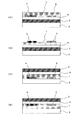
次に、図面を参照しながら本発明の好ましい実施の形態について説明を行う。まず、図1を参照しながら、有機薄膜トランジスタ(有機TFT)の構成とその動作について説明する。図1(A)〜(D)は、本発明の有機TFTの構成例である。なお、図1中、符号1は有機半導体層、符号2は基板、符号3はゲート電極、符号4はソース電極、符号5はドレイン電極、符号6は絶縁層である。このTFTデバイスは、基板2より上に空間的に分離されたゲート電極3、ソース電極4、ドレイン電極5が設けられており、ゲート電極3と有機半導体層1の間には絶縁層6(ゲート絶縁膜)が設けられている。TFTデバイスはゲート電極3への電圧の印加により、ソース電極4とドレイン電極5の間の有機半導体層1内を流れる電流がコントロールされる。
Next, a preferred embodiment of the present invention will be described with reference to the drawings. First, the structure and operation of an organic thin film transistor (organic TFT) will be described with reference to FIG. 1A to 1D are configuration examples of the organic TFT of the present invention. In FIG. 1,
図1(A)は代表的な有機TFTの断面図であるが、材料以外の構造に関する説明を、この図1(A)を参照しながら説明する。図1(A)中の一対の電極(ソース電極4およびドレイン電極5)の間に電圧をかけると、有機半導体層1を通じてソース電極4とドレイン電極5の間に電流が流れる。この際、絶縁層6により有機半導体層1と隔てられたゲート電極3に電圧を印加すると、電界効果によって有機半導体層1の電導度が変化し、したがってソース・ドレイン電極間に流れる電流を変調することができる。これは絶縁層に近接する有機半導体層1内の蓄積層の幅がゲート電圧によって変化し、チャネル断面積が変化するためであると考えられている。
FIG. 1A is a cross-sectional view of a typical organic TFT. A description of a structure other than the material will be given with reference to FIG. When a voltage is applied between the pair of electrodes (
図1(A)は、絶縁層6の上にソースあるいはドレイン電極4,5があり、その上に有機半導体層1が形成されたボトムコンタクトタイプと呼ばれる。また、図1(B)は、有機半導体層1の上にソースあるいはドレイン電極4,5が形成されたトップコンタクトタイプと言われる。図1(C)および(D)は、絶縁層6およびゲート電極3を有機半導体層1の上に設けたものである。
FIG. 1A is called a bottom contact type in which source or
本発明の有機TFTにおいて、有機半導体層1は、図1(A)〜(D)に示す様にいずれの構造においてもソース電極4およびドレイン電極5に挟まれるようになっている。有機半導体層1の厚みは、約1000nm〜約5nmが好ましい。従って、粒径のあまり大きな顔料の分散液は好ましくない。溶液中での平均粒径は1000nm以下が好ましく、300nm以下がより好ましい。
In the organic TFT of the present invention, the
本発明の有機TFTは、通常、例えばガラス、シリコン、プラスチック等よりなる基板2に形成される。デバイスにフレキシビリティー、軽量、安価等の特性が所望される場合、通常はプラスチック基板が用いられる。また、図1(A)、(B)に示すトランジスタ構造の場合には、基板2として導電性基板を用いることにより、ゲート電極3を兼ねる事が可能である。
The organic TFT of the present invention is usually formed on a
本発明のデバイスは、3つの空間的に分離された電極(ソース電極4、ドレイン電極5、ゲート電極3)を有する。ゲート電極3は、絶縁層6と接触している。各電極は周知の従来技術を用いて基板2上に形成することができる。ソース電極4、ドレイン電極5、ゲート電極3の材質としては、導電性材料であれば特に限定されず、例えば白金、金、銀、ニッケル、クロム、銅、鉄、錫、アンチモン、鉛、タンタル、インジウム、アルミニウム、亜鉛、マグネシウム、およびこれらの合金や、インジウム・錫酸化物等の導電性金属酸化物、あるいはドーピング等で導電率を向上させた無機および有機半導体、例えばシリコン単結晶、ポリシリコン、アモルファスシリコン、ゲルマニウム、グラファイト、ポリアセチレン、ポリパラフェニレン、ポリチオフェン、ポリピロール、ポリアニリン、ポリチエニレンビニレン、ポリパラフェニレンビニレン等が挙げられる。ソース電極4およびドレイン電極5は、上記導電性物質の中でも有機半導体層1との接触面においてオーミックに接続されるものが好ましい。
The device of the present invention has three spatially separated electrodes (
また、絶縁層6はゲート電極3及び有機半導体層1の間に配置される。好適な絶縁材料は当業者には周知である。絶縁材料としては、例えば、酸化シリコン、窒化シリコン、酸化アルミニウム、窒化アルミニウム、酸化チタン等の無機系材料や、またはフレキシビリティー、軽量、安価なデバイスが所望される場合には、例えばポリイミド、ポリビニルアルコール、ポリビニルフェノール、ポリエステル、ポリエチレン、ポリフェニレンスルフィド、ポリパラキシリレン、ポリアクリロニトリル、シアノエチルプルラン、ポリカーボネート等をはじめとする高分子化合物や、各種絶縁性LB膜等の種々の有機系材料を挙げることができる。これらの材料は、2つ以上を組み合わせて用いてもよい。本発明において、絶縁材料の種類は特に限定されないが、導電率が低いものが好ましい。なお、シリコンを、ゲート電極3と基板2の両方に用いる場合には、シリコンの熱酸化により得られる酸化シリコンも絶縁層3として使うことができる。
The insulating
絶縁層6の作製法としては特に制限はなく、例えばCVD法、プラズマCVD法、プラズマ重合法、蒸着法、スピンコーティング法、ディッピング法、印刷法、インクジェット法、LB法などが挙げられ、いずれも使用可能である。
There is no restriction | limiting in particular as a preparation method of the insulating
上記構成を有する有機TFTにおいて、有機半導体層1の材料として、有機溶媒に溶解しやすい有機半導体を使用した場合、図1(C)および(D)の構造では、有機溶媒に溶解した材料で絶縁層6を塗布すると、有機半導体層1が溶解してしまうという不都合がある。しかし、本発明のように有機溶媒に難溶の顔料を分散させたインク(有機顔料分散液)で作成した有機半導体層の場合は、有機溶媒に接触しても有機半導体層1が溶解するようなことはないため、絶縁層6を、例えばポリカーボネートなどを有機溶媒に溶解した液で作成する場合でも、有機半導体層1に影響を与えずに湿式成膜が可能となる。
In the organic TFT having the above configuration, when an organic semiconductor that is easily dissolved in an organic solvent is used as the material of the
また、図1(A)および(B)のような構成でも、本発明のように、有機溶媒に溶解しにくい有機顔料分散液で作成した有機半導体層1は、有機溶媒による影響を受けないので、有機溶媒に溶解し易い材料と有機溶媒を使用し、保護層(図示せず)を湿式法で作成することが可能となる。
1A and 1B, the
[有機顔料分散液]
本発明の有機顔料分散液は、有機溶媒と、この有機溶媒中に分散した有機顔料と、を含有する組成物である。
[Organic pigment dispersion]
The organic pigment dispersion of the present invention is a composition containing an organic solvent and an organic pigment dispersed in the organic solvent.
本発明において、有機顔料とは、特に可視域に吸収をもたなくてもよく、その定義としては、結晶状態の有機物粉体で、結晶内部のキャリア(電子、正孔)の移動度が高いものであればいずれの粉体も含まれる。また、本発明で使用する有機顔料は、有機溶媒に溶解しにくい有機半導体材料が好ましく、例えばアゾ顔料、ビスアゾ顔料、ペリレン顔料、金属フタロシアニン顔料、無金属フタロシアニン顔料、アンサンスロン顔料などを挙げることができる。有機顔料としては、有機溶媒への溶解度が、0.1重量%以下ものがより好ましい。 In the present invention, the organic pigment may not have absorption in the visible region, and is defined as a crystalline organic powder having high mobility of carriers (electrons and holes) inside the crystal. Any powder can be included. In addition, the organic pigment used in the present invention is preferably an organic semiconductor material that is difficult to dissolve in an organic solvent, and examples thereof include azo pigments, bisazo pigments, perylene pigments, metal phthalocyanine pigments, metal-free phthalocyanine pigments, ansanthrone pigments, and the like. it can. As the organic pigment, those having a solubility in an organic solvent of 0.1% by weight or less are more preferable.
本発明において好ましく使用できる有機顔料の一例として以下の一般式(I)で表されるジスアゾ化合物を挙げることができる。 An example of an organic pigment that can be preferably used in the present invention is a disazo compound represented by the following general formula (I).
[式(I)中、Xは置換あるいは無置換の、芳香環内にヘテロ原子を有していてもよい芳香族基であり、R1,R2は同一または異なって、水素原子、ハロゲン原子、アルキル基、アルコキシ基、シアノ基、アミノ基のいずれかを意味する。ただし、R1,R2はそれぞれ同一のベンゼン環に複数結合していてもよい。] [In the formula (I), X is a substituted or unsubstituted aromatic group which may have a hetero atom in the aromatic ring, and R 1 and R 2 are the same or different and each represents a hydrogen atom or a halogen atom. , An alkyl group, an alkoxy group, a cyano group, or an amino group. However, a plurality of R 1 and R 2 may be bonded to the same benzene ring. ]
一般式(I)の化合物において、実験の結果、基Xとして例えばフルオレノン、アントラキノン、ベンゾフェノン、チオキサントン構造など、電子吸引性を有する2価の芳香族基を選定することにより、電子輸送性の有機トランジスタ特性を示したものが得られる。電子輸送性の材料は希少であり、これらの材料は、湿式法のみならず、蒸着によって有機半導体層を形成する場合でも有効である。 In the compound of the general formula (I), as a result of experiments, by selecting a divalent aromatic group having an electron-withdrawing property, such as a fluorenone, anthraquinone, benzophenone, thioxanthone structure, as the group X, an electron-transporting organic transistor A characteristic is obtained. Electron transporting materials are rare, and these materials are effective not only for wet methods but also for forming an organic semiconductor layer by vapor deposition.
また、基Xを下記構造とするとホール移動性を示した(なお、下記構造において芳香環には置換基がついていてもよい)。 Moreover, when the group X had the following structure, hole mobility was shown (in the structure below, the aromatic ring may have a substituent).
また、有機顔料の別の例として、下記構造のトリスアゾ顔料でもよい。 As another example of the organic pigment, a trisazo pigment having the following structure may be used.
さらに、有機顔料としては、下記構造のフタロシアニン顔料でもよい。 Further, the organic pigment may be a phthalocyanine pigment having the following structure.
[式中、Zは、銅、ニッケル、鉄、チタニウムオキシドの金属原子か、または無金属原子を意味し、Y1,Y2,Y3,Y4は、ハロゲン基、アルキル基、アルキルスルホニル基を意味し、k,l,m,nは独立して0から4の数を意味する。] [Wherein Z represents a metal atom of copper, nickel, iron, titanium oxide or a metal-free atom, and Y 1 , Y 2 , Y 3 , Y 4 represent a halogen group, an alkyl group, or an alkylsulfonyl group. And k, l, m, and n independently represent a number from 0 to 4. ]
上記ジスアゾ顔料は、電子顕微鏡でみると、数十nm以下の糸状をしており、層は糸が折り重なった構造と思われ、溶液中の平均粒径から想定されるよりも、薄い膜を作成するのに有利である。また、フタロシアニン顔料は、粒径が大きくなりがちであるが、硫酸に溶解後、水中に滴下することにより比較的小粒径のアモルファスとすることができる。 The disazo pigment has a thread shape of several tens of nanometers or less when viewed with an electron microscope, and the layer seems to be a structure in which the yarn is folded, creating a thinner film than expected from the average particle size in the solution. It is advantageous to do. The phthalocyanine pigment tends to have a large particle size, but it can be made amorphous with a relatively small particle size by being dropped into water after being dissolved in sulfuric acid.
本発明の有機顔料分散液に含有される有機溶媒としては、有機顔料の分散が可能な溶媒であれば、いずれもよいが、有機顔料が例えばジスアゾ顔料の場合、アノン系の溶媒が好ましい。また、有機顔料がフタロシアニン顔料である場合には、例えばケトン系、エーテル系の溶媒が好ましい。 The organic solvent contained in the organic pigment dispersion of the present invention may be any solvent that can disperse the organic pigment, but when the organic pigment is, for example, a disazo pigment, an anone-based solvent is preferable. Further, when the organic pigment is a phthalocyanine pigment, for example, a ketone solvent or an ether solvent is preferable.
本発明の有機顔料分散液には、上記有機溶媒と有機顔料のほかに、分散樹脂(導電性のものでもよい)、や、場合により、レベリング性をもたせるための界面活性剤、酸化防止剤、消泡剤等の任意成分を配合することもできる。 In the organic pigment dispersion of the present invention, in addition to the organic solvent and the organic pigment, a dispersion resin (which may be conductive), or a surfactant for imparting leveling properties in some cases, an antioxidant, Optional components such as an antifoaming agent can also be blended.
また、有機顔料分散液は、例えば有機顔料と有機溶媒とを混合し、有機顔料を有機溶媒中に分散させることにより調製できる。分散の方法は問われず、例えば、ジルコニアボールなどを使用してボールミル分散をしてもよい。また、湿式分散機[例えばダイノーミル KDL A型(WAB社製)]を使用してもよい。有機顔料の粉体を有機溶媒中に分散させる際、有機顔料の平均粒径は、有機半導体層を極力薄膜化する観点から、1000nm以下(例えば1000nm以下1nm以上)とすることが好ましく、50nm以下(例えば50nm以下1nm以上)とすることがより好ましい。また、本発明の有機顔料分散液における有機溶媒と有機顔料との配合比率は、分散性の観点から、5〜200部対1部とすることが好ましい。また、場合により、製膜性の観点から、分散樹脂を有機顔料1部に対し、0〜1部いれる。 The organic pigment dispersion can be prepared, for example, by mixing an organic pigment and an organic solvent and dispersing the organic pigment in the organic solvent. The dispersion method is not limited, and for example, ball mill dispersion may be performed using zirconia balls or the like. Moreover, you may use a wet disperser [For example, dyno mill KDL A type (made by WAB company)]. When dispersing the organic pigment powder in the organic solvent, the average particle diameter of the organic pigment is preferably 1000 nm or less (for example, 1000 nm or less and 1 nm or more) from the viewpoint of making the organic semiconductor layer as thin as possible, and 50 nm or less. More preferably (for example, 50 nm or less and 1 nm or more). In addition, the blending ratio of the organic solvent and the organic pigment in the organic pigment dispersion of the present invention is preferably 5 to 200 parts to 1 part from the viewpoint of dispersibility. In some cases, from the viewpoint of film forming properties, 0 to 1 part of the dispersion resin is added to 1 part of the organic pigment.
[湿式塗布工程]
本発明の有機顔料分散液は、湿式法にて対象物の上に塗布された後、乾燥させられる。湿式法に関しては、例えばスピンコーティング、孔版印刷、オフセット印刷、インクジェット印刷法などの周知の印刷法によって成膜することができる。スピンコーティングは、例えば回転による遠心力を用い、基板に塗膜を形成する方法である。しかしながら、スピンコーティングには、回転により、回転体(基板)と空気界面での相対的な位置変化にともなう、いわゆる風の影響により、溶媒の急激な乾燥が生じ、均一な塗布成膜ができないという問題がある。従って、カップスピン法にて成膜することが好ましい。
[Wet coating process]
The organic pigment dispersion of the present invention is applied onto an object by a wet method and then dried. As for the wet method, the film can be formed by a known printing method such as spin coating, stencil printing, offset printing, and ink jet printing. Spin coating is a method of forming a coating film on a substrate using, for example, centrifugal force due to rotation. However, in spin coating, due to the relative position change at the rotating body (substrate) and the air interface due to rotation, the so-called wind causes drastic drying of the solvent, and uniform coating cannot be formed. There's a problem. Therefore, it is preferable to form a film by a cup spin method.
カップスピン法は、次の工程(1)及び(2)によって行なわれる方法である。
(1)カップ(容器)の底面に、基板を固定し、コーティング溶液を配置させる。
(2)その後、容器を密閉し(蓋をする)、容器ごと回転し、成膜する。
上記カップスピン法の利点は、密閉空間内では、回転体と空気の相対的な位置変化が生じず、風の影響を受けない点と、溶媒の蒸気で密閉空間が飽和され、急激な乾燥を防止することができる点が挙げられる。ただし、本発明方法において有機半導体層1は、カップスピン法でなくても成膜が可能である。
The cup spin method is performed by the following steps (1) and (2).
(1) The substrate is fixed to the bottom surface of the cup (container), and the coating solution is disposed.
(2) Thereafter, the container is sealed (covered), and the whole container is rotated to form a film.
The advantages of the cup-spin method are that the relative position of the rotating body and air does not change in the enclosed space and is not affected by the wind, and the enclosed space is saturated with the vapor of the solvent, so that rapid drying is possible. The point which can be prevented is mentioned. However, in the method of the present invention, the
一方、インクジェットプリント技術を応用し、有機顔料分散液を微小液滴として吐出して下地層の上にドットまたは層を作製できる液滴吐出法による印刷も可能である。その場合、塗れ性をよくするために、有機顔料分散液中に、各種界面活性剤を添加してもよい。特にフッ素やシリコン系のノニオン系界面活性剤が好ましい。 On the other hand, it is possible to perform printing by a droplet discharge method in which dots or layers can be formed on an underlying layer by applying an inkjet printing technique and discharging an organic pigment dispersion as fine droplets. In that case, in order to improve paintability, various surfactants may be added to the organic pigment dispersion. In particular, fluorine and silicon nonionic surfactants are preferred.
[乾燥工程]
湿式塗布後は、有機溶媒を除去して有機半導体層を形成するために乾燥させる。乾燥方法は特に制限はないが、加熱乾燥が好ましい。本発明の有機半導体層の形成に関しては、加熱温度がキャリアの移動度に影響を与えることから、溶媒乾燥の処理温度を余り高くすることは好ましくなく、例えば200℃以下の処理温度で乾燥させることが望ましい。
[Drying process]
After the wet coating, the organic solvent is removed to form an organic semiconductor layer and then dried. Although there is no restriction | limiting in particular in the drying method, Heat drying is preferable. Regarding the formation of the organic semiconductor layer of the present invention, since the heating temperature affects the mobility of carriers, it is not preferable to set the treatment temperature for solvent drying too high, for example, drying at a treatment temperature of 200 ° C. or less. Is desirable.
本発明においては、後記実施例に示したように、アゾ顔料のような溶媒に溶解しない材料でも分散液として塗布することにより、有機トランジスタ特性を示すことが可能な有機半導体層を形成できることが確認された。このことから、湿式成膜技術にて簡便に、コストパフォーマンスに優れた有機薄膜トランジスタを製造できる。また、特にインクジェットプリント技術を応用した液滴吐出法で簡易に印刷可能であるという利点もある。 In the present invention, it was confirmed that an organic semiconductor layer capable of exhibiting organic transistor characteristics can be formed by applying a material that does not dissolve in a solvent such as an azo pigment as a dispersion, as shown in Examples below. It was done. From this, an organic thin film transistor excellent in cost performance can be easily manufactured by a wet film forming technique. In addition, there is an advantage that printing can be easily performed by a droplet discharge method that applies an inkjet printing technique.
なお、本発明の有機半導体層の場合、有機顔料が有機溶媒に溶解しないため、上層に絶縁層あるいは保護層を設ける場合に、有機溶媒を含有した塗工液が使用可能である。すなわち、例えば各種ポリカーボネート、ポリエステル、ポリスチレン樹脂などを有機溶媒に溶解させて、塗工することが可能である。なお、この場合、塗工液中に、誘電率を調整するための無機材料を添加分散してもよい。 In the case of the organic semiconductor layer of the present invention, since the organic pigment is not dissolved in the organic solvent, a coating solution containing an organic solvent can be used when an insulating layer or a protective layer is provided on the upper layer. That is, for example, various polycarbonates, polyesters, polystyrene resins and the like can be dissolved in an organic solvent and applied. In this case, an inorganic material for adjusting the dielectric constant may be added and dispersed in the coating solution.
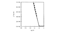
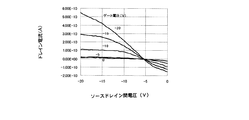
次に、実施例、比較例を挙げ、本発明をさらに詳しく説明するが、本発明はこれによって制約されるものではない。まず、実施例等で行ったトランジスタの性能評価方法について図2及び3を用いて説明する。有機半導体の電界効果によるキャリア移動度は、以下の式を用いて算出される。 EXAMPLES Next, although an Example and a comparative example are given and this invention is demonstrated in more detail, this invention is not restrict | limited by this. First, a transistor performance evaluation method performed in Examples and the like will be described with reference to FIGS. The carrier mobility due to the electric field effect of the organic semiconductor is calculated using the following equation.
[ただし、Cinはゲート絶縁膜の単位面積当たりのキャパシタンス、Wはチャネル幅、Lはチャネル長、Vgはゲート電圧、Idsはソース・ドレイン電流、μはキャリアの移動度、Vthはチャネルが形成し始めるゲートの閾値電圧である。] [Where C in is the capacitance per unit area of the gate insulating film, W is the channel width, L is the channel length, V g is the gate voltage, I ds is the source / drain current, μ is the carrier mobility, and V th is The threshold voltage of the gate where the channel begins to form. ]
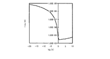
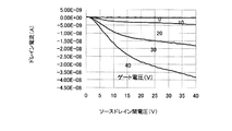
図2は、ソース・ドレイン間の電圧Vds=−20[V]における有機TFTの特性を示すグラフの一例である(なお、あくまでも例示であり、本発明の有機TFTのデータではない)。 FIG. 2 is an example of a graph showing the characteristics of the organic TFT at the source-drain voltage Vds = −20 [V] (note that this is merely an example and not the data of the organic TFT of the present invention).
図2に示すように、ソース・ドレイン間に−20[V]を印加して、ゲート電圧を10から−20[V]挿引した際のソース・ドレイン電流を測定する。なお、図2に示すグラフ中、Vg=−20[V]におけるIds値が、有機TFTのオン電流となる。 As shown in FIG. 2, -20 [V] is applied between the source and the drain, and the source / drain current when the gate voltage is subtracted from 10 to -20 [V] is measured. In the graph shown in FIG. 2, the Ids value at Vg = −20 [V] is the ON current of the organic TFT.
また、図3に示すように、上記条件で測定されたソース・ドレイン電流の平方根をゲート電圧に対しプロットして直線近似を行なう(図3も一例である)。近似曲線においてソース・ドレイン電流の平方根が0[A]になるゲート電圧値を閾値電圧Vthと定義する。 Further, as shown in FIG. 3, the square root of the source / drain current measured under the above conditions is plotted against the gate voltage to perform linear approximation (FIG. 3 is also an example). The gate voltage value at which the square root of the source / drain current in the approximate curve becomes 0 [A] is defined as the threshold voltage Vth.
[実施例1]
有機半導体塗工液の作成:
以下の構造式のジスアゾ顔料を合成した。なお、このジスアゾ顔料は公知化合物である(例えば特開平3−230168号公報参照)。
[Example 1]
Preparation of organic semiconductor coating solution:
A disazo pigment having the following structural formula was synthesized. This disazo pigment is a known compound (for example, see JP-A-3-230168).
得られた粗結晶8.0gを800mlのN,N−ジメチルホルムアミド(DMF)に分散し、80℃で2時間撹拌洗浄する操作を3回繰り返した。その後、結晶をイオン交換水1000mlで2回洗浄して、減圧下120℃で乾燥した。 The operation of dispersing 8.0 g of the obtained crude crystals in 800 ml of N, N-dimethylformamide (DMF) and stirring and washing at 80 ° C. for 2 hours was repeated three times. Thereafter, the crystals were washed twice with 1000 ml of ion exchange water and dried at 120 ° C. under reduced pressure.
口径6cmのガラスポット中に、その容積のおよそ1/2量となるように、直径5mmYTZ(部分安定化ジルコニア)ボールを入れ、さらに、上記のジスアゾ顔料を1.0g、ポリビニルブチラール(ユニオンカーバイド社製 XYHL)0.1g、シクロヘキサノン22.9gを入れて4日間かけてボールミルで分散した。分散終了後、シクロヘキサノン24gを追加して撹拌後、ミルベース30gを取り出して、撹拌しながらメチルエチルケトン/シクロヘキサノン(27.6g/34.8g)で滴下稀釈して塗工用インクとした。この塗工用インク中の分散粒子の平均粒径は、堀場製作所製粒子径測定器CAPA−500(商品名)で測定した結果、約110nmであった。 In a glass pot with a diameter of 6 cm, a 5 mm diameter YTZ (partially stabilized zirconia) ball is placed so that the volume is approximately ½ of the volume. Further, 1.0 g of the above disazo pigment, polyvinyl butyral (Union Carbide) (XYHL manufactured) 0.1 g and cyclohexanone 22.9 g were added and dispersed with a ball mill for 4 days. After the completion of dispersion, 24 g of cyclohexanone was added and stirred, and then 30 g of mill base was taken out and diluted dropwise with methyl ethyl ketone / cyclohexanone (27.6 g / 34.8 g) while stirring to obtain a coating ink. The average particle size of the dispersed particles in this coating ink was about 110 nm as a result of measurement using a particle size measuring device CAPA-500 (trade name) manufactured by Horiba.
基板の作成:
シリコン基板表面を熱酸化してSiO2の絶縁膜を300nm形成した基板を用意した。この基板を硫酸:過酸化水素=4:1で気泡が出なくなるまで洗浄し、水洗し、ヘキサメチルジシラザンで表面処理し、110℃で乾燥した。乾燥後、この基板上に、フォトレジスト法でクロムを1オングストローム(0.1nm)の厚み、金を500オングストローム(50nm)の厚みでソース・ドレイン電極のパターンを形成した。チャネル長は25μm、チャネル幅は7.6mmとした。この上に前記塗工用インクをスピンコート法(1500回転;30秒)で塗工した。これを120℃、15分間かけて乾燥させた。
Board creation:
A substrate was prepared in which the silicon substrate surface was thermally oxidized to form an SiO 2 insulating film having a thickness of 300 nm. This substrate was washed with sulfuric acid: hydrogen peroxide = 4: 1 until no bubbles were generated, washed with water, surface-treated with hexamethyldisilazane, and dried at 110 ° C. After drying, a pattern of source / drain electrodes was formed on the substrate by a photoresist method with a thickness of 1 angstrom (0.1 nm) of chromium and a thickness of 500 angstrom (50 nm) of gold. The channel length was 25 μm and the channel width was 7.6 mm. On top of this, the coating ink was applied by spin coating (1500 rpm; 30 seconds). This was dried at 120 ° C. for 15 minutes.
このように作製した有機薄膜トランジスタの特性である電界効果移動度を測定した。なお、有機薄膜トランジスタの電界効果移動度の算出には、以下の式を用いた。 The field effect mobility, which is a characteristic of the organic thin film transistor thus fabricated, was measured. In addition, the following formula | equation was used for calculation of the field effect mobility of an organic thin-film transistor.
[ただし、Cinはゲート絶縁膜の単位面積あたりのキャパシタンス、Wはチャネル幅、Lはチャネル長、Vgはゲート電圧、Idsはソース・ドレイン電流、μは移動度、Vthはチャネルが形成し始めるゲートの閾値電圧である。] [Where C in is the capacitance per unit area of the gate insulating film, W is the channel width, L is the channel length, V g is the gate voltage, I ds is the source / drain current, μ is the mobility, and V th is the channel. This is the threshold voltage of the gate that begins to form. ]
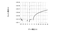
作成した薄膜トランジスタの特性を評価したところ、電界効果移動度2.7×10⁻⁵cm2/Vs、閾値電圧7V、オンオフ比1.2×103の特性を示し、電子移動性を有していた。ホール移動性は小さかった。図4に作製したトランジスタのVds=−40Vの際の伝達特性を示し、図5に出力特性を示した。このようにジスアゾ化合物の中心骨格がフルオレノンやアントラキノンなど電子吸引性のものは良好な電子移動剤としてトランジスタに利用可能であった。なお、このジスアゾ顔料は溶媒中での平均粒径は110nmとまだ大きめであるが、電子顕微鏡でみると構造的に径が数十nm以下の糸状を有しており、顔料分散液であっても塗工後に薄膜を形成しやすい長所があることが確認された。 When the characteristics of the thin film transistor thus fabricated were evaluated, the field effect mobility was 2.7 × 10 −5 cm 2 / Vs, the threshold voltage was 7 V, the on / off ratio was 1.2 × 10 3 , and the electron mobility was exhibited. It was. Hall mobility was small. FIG. 4 shows the transfer characteristics of the manufactured transistor when Vds = −40 V, and FIG. 5 shows the output characteristics. As described above, those having an electron-withdrawing property such as fluorenone and anthraquinone having a central skeleton of a disazo compound can be used for a transistor as a good electron transfer agent. Note that this disazo pigment has an average particle size of 110 nm in the solvent, which is still large, but when viewed with an electron microscope, it has a thread shape with a diameter of several tens of nm or less. It was also confirmed that there is an advantage that a thin film can be easily formed after coating.
[実施例2]
サンプル瓶に2mm径のジルコニアビーズを入れて、シクロヘプタノン3重量部、メチルエチルケトン0.84重量部、下記構造のアゾ顔料0.043重量部を添加し、1時間かけてミリングした。
[Example 2]
Zirconia beads having a diameter of 2 mm were placed in a sample bottle, 3 parts by weight of cycloheptanone, 0.84 parts by weight of methyl ethyl ketone, and 0.043 parts by weight of an azo pigment having the following structure were added and milled for 1 hour.
ミリング終了後の混合物に、4%重量のブチラール樹脂(積水化学工業-商品名BM−S)の溶液(溶媒はメチルエチルケトン)0.21重量部を添加してさらに5時間ミリングした。なお、分散粒子の平均粒径は、350nmであった。これを実施例1と同様に基板にスピンコート法で塗布し、120℃で15分間乾燥させ、有機薄膜トランジスタを作製した。移動度は1.2×10⁻⁶cm2/Vsでホール移動性を示した。図6に、作製したトランジスタの伝達特性を示し、図7に出力特性を示した。 To the mixture after milling, 0.21 part by weight of a 4% by weight solution of butyral resin (Sekisui Chemical Co., Ltd., trade name: BM-S) (solvent is methyl ethyl ketone) was added and milled for another 5 hours. The average particle size of the dispersed particles was 350 nm. This was applied to the substrate by spin coating as in Example 1, and dried at 120 ° C. for 15 minutes to produce an organic thin film transistor. The mobility was 1.2 × 10 −6 cm 2 / Vs, indicating hole mobility. FIG. 6 shows the transfer characteristics of the manufactured transistor, and FIG. 7 shows the output characteristics.
[実施例3]
オキシチタニウムフタロシアニン(CuKαを用いたX線回折における回折角2θ±0.2°の27.1°に強いピークを有する)1.8重量部、ブチラール樹脂1.2重量部、メチルエチルケトン97重量部のミリング溶液を実施例1と同様にして基板にスピンコートした。分散粒子の平均粒径は、およそ1μmであった。実施例1と同様に有機薄膜トランジスタを作製し、電気的特性を調べた。その結果、移動度は5×10⁻⁷cm2/Vsでホール移動性を示した。
[Example 3]
1.8 parts by weight of oxytitanium phthalocyanine (having a strong peak at 27.1 ° of diffraction angle 2θ ± 0.2 ° in X-ray diffraction using CuKα), 1.2 parts by weight of butyral resin, 97 parts by weight of methyl ethyl ketone The milling solution was spin coated on the substrate as in Example 1. The average particle diameter of the dispersed particles was approximately 1 μm. An organic thin film transistor was produced in the same manner as in Example 1, and the electrical characteristics were examined. As a result, the mobility was 5 × 10 −7 cm 2 / Vs and the hole mobility was shown.
[実施例4]
ポリカーボネート樹脂[ポリカーボネートZポリカ(帝人化成社製)]1重量部及びテトラヒドロフラン100重量部を混合溶解した後、これを実施例1で作製した有機半導体層上にスピンコートで塗布し、80℃で2分間、140℃で15分間乾燥して保護層を作成した。しかし、下層の有機顔料分散液で作成した有機半導体層が溶解することはなかった。このポリカーボネート層の上部にゲート電極を設ければ、この層は絶縁層としても利用可能である。
[Example 4]
After mixing and dissolving 1 part by weight of polycarbonate resin [Polycarbonate Z Polyca (manufactured by Teijin Chemicals Ltd.)] and 100 parts by weight of tetrahydrofuran, this was coated on the organic semiconductor layer produced in Example 1 by spin coating, and 2 parts at 80 ° C. A protective layer was prepared by drying for 15 minutes at 140 ° C. for 15 minutes. However, the organic semiconductor layer prepared with the lower organic pigment dispersion did not dissolve. If a gate electrode is provided on the polycarbonate layer, this layer can also be used as an insulating layer.
[比較例1]
実施例1の有機顔料分散液の替りに下記構造の有機高分子半導体を塗布した層の上に実施例4のポリカーボネートを含む塗工液を塗布した。この有機高分子半導体はテトラヒドロフランに溶解してしまうため、チャネル部は溶解破壊されてしまった。従って、このような有機半導体層の上には、有機溶媒液による湿式塗布法での絶縁層あるいは保護層の作成はできなかった。
[Comparative Example 1]
Instead of the organic pigment dispersion of Example 1, the coating liquid containing the polycarbonate of Example 4 was applied on the layer coated with the organic polymer semiconductor having the following structure. Since the organic polymer semiconductor is dissolved in tetrahydrofuran, the channel portion is dissolved and broken. Therefore, an insulating layer or protective layer could not be formed on such an organic semiconductor layer by a wet coating method using an organic solvent solution.
[式中、qは1〜10000の数を意味する]
また、本比較例では分子量が約10万となるようなqの個数のものを用いた。
[Wherein q means a number of 1 to 10,000]
Further, in this comparative example, a q number having a molecular weight of about 100,000 was used.
なお、本発明は上記各実施の形態に限定されず、種々の変更が可能である。例えば、有機溶媒に溶解し易い材料で、結晶化した場合に高移動度を示すような材料においても、従来のように、有機溶媒に溶解させ、塗布し、絶縁層上で結晶化させる方法をとると、結晶がどうしても不均一にできてしまうという弊害が生じる。そのような場合も、有機溶媒を選択し、すでに結晶化している固体物を、溶解しにくい貧溶媒中で分散させ、塗工する方法もある。この場合、結晶間に粒界はできてしまうが、必ず結晶間に電荷の伝わる点が少なからず形成されるため、絶縁層上で結晶化させるときのような、幅の広い大きな断絶で全く電流が通りにくくなるようなことはなく、トランジスタ各素子で特性を均一化させることができる。 In addition, this invention is not limited to said each embodiment, A various change is possible. For example, a material that is easily dissolved in an organic solvent and that exhibits high mobility when crystallized can be dissolved in an organic solvent, applied, and crystallized on an insulating layer as in the past. In this case, there is an adverse effect that crystals are inevitably made non-uniform. Even in such a case, there is a method in which an organic solvent is selected, and a solid material that has already crystallized is dispersed in a poor solvent that is difficult to dissolve, and coating is performed. In this case, a grain boundary is formed between the crystals, but since there are not a few points where charges are transmitted between the crystals, there is no current at all due to a wide and wide break such as when crystallizing on the insulating layer. Is not difficult to pass, and the characteristics of each transistor element can be made uniform.
1…有機半導体層
2…基板
3…ゲート電極
4…ソース電極
5…ドレイン電極
6…絶縁層
DESCRIPTION OF
Claims (10)
少なくとも有機溶媒と、この有機溶媒中に分散した有機顔料と、を含有することを特徴とする有機顔料分散液。 An organic pigment dispersion used as a coating liquid when an organic semiconductor layer in an organic transistor is formed by a wet coating method,
An organic pigment dispersion comprising at least an organic solvent and an organic pigment dispersed in the organic solvent.
[式(I)中、Xは置換あるいは無置換の、芳香環内にヘテロ原子を有していてもよい芳香族基であり、R1,R2は同一または異なって、水素原子、ハロゲン原子、アルキル基、アルコキシ基、シアノ基、アミノ基のいずれかを意味する。ただし、R1,R2はそれぞれ同一のベンゼン環に複数結合していてもよい。] The organic pigment dispersion according to claim 2, wherein the azo organic pigment is an azo pigment represented by the following general formula (I).
[In the formula (I), X is a substituted or unsubstituted aromatic group which may have a hetero atom in the aromatic ring, and R 1 and R 2 are the same or different and each represents a hydrogen atom or a halogen atom. , An alkyl group, an alkoxy group, a cyano group, or an amino group. However, a plurality of R 1 and R 2 may be bonded to the same benzene ring. ]
有機溶媒と、この有機溶媒中に分散したアゾ系またはフタロシアニン系の有機顔料と、を含有する有機顔料分散液を下地層の上に湿式塗布することを特徴とする有機半導体層の形成方法。 A method for forming an organic semiconductor layer in an organic transistor,
A method for forming an organic semiconductor layer, comprising wet-coating an organic pigment dispersion containing an organic solvent and an azo- or phthalocyanine-based organic pigment dispersed in the organic solvent on an underlayer.
前記有機半導体層の上層に、有機溶媒で樹脂を溶解もしくは分散させた液を付着させることにより、絶縁層または保護層を形成する工程と、
を備えたことを特徴とする有機トランジスタの製造方法。 Forming an organic semiconductor layer by the method for forming an organic semiconductor layer according to any one of claims 5 to 7,
A step of forming an insulating layer or a protective layer by adhering a liquid obtained by dissolving or dispersing a resin in an organic solvent to the upper layer of the organic semiconductor layer;
A method for producing an organic transistor, comprising:
[式(I)中、Xは置換あるいは無置換の、芳香環内にヘテロ原子を有していてもよい芳香族基であり、R1,R2は同一または異なって、水素原子、ハロゲン原子、アルキル基、アルコキシ基、シアノ基、アミノ基のいずれかを意味する。ただし、R1,R2はそれぞれ同一のベンゼン環に複数結合していてもよい。] An organic transistor comprising a layer containing a substance represented by the following general formula (I) as an electron transporting material.
[In the formula (I), X is a substituted or unsubstituted aromatic group which may have a hetero atom in the aromatic ring, and R 1 and R 2 are the same or different and each represents a hydrogen atom or a halogen atom. , An alkyl group, an alkoxy group, a cyano group, or an amino group. However, a plurality of R 1 and R 2 may be bonded to the same benzene ring. ]
Priority Applications (1)
| Application Number | Priority Date | Filing Date | Title |
|---|---|---|---|
| JP2008236803A JP5648775B2 (en) | 2008-09-16 | 2008-09-16 | Organic pigment dispersion, organic semiconductor layer forming method, organic transistor manufacturing method, and organic transistor |
Applications Claiming Priority (1)
| Application Number | Priority Date | Filing Date | Title |
|---|---|---|---|
| JP2008236803A JP5648775B2 (en) | 2008-09-16 | 2008-09-16 | Organic pigment dispersion, organic semiconductor layer forming method, organic transistor manufacturing method, and organic transistor |
Publications (2)
| Publication Number | Publication Date |
|---|---|
| JP2010070596A true JP2010070596A (en) | 2010-04-02 |
| JP5648775B2 JP5648775B2 (en) | 2015-01-07 |
Family
ID=42202701
Family Applications (1)
| Application Number | Title | Priority Date | Filing Date |
|---|---|---|---|
| JP2008236803A Expired - Fee Related JP5648775B2 (en) | 2008-09-16 | 2008-09-16 | Organic pigment dispersion, organic semiconductor layer forming method, organic transistor manufacturing method, and organic transistor |
Country Status (1)
| Country | Link |
|---|---|
| JP (1) | JP5648775B2 (en) |
Cited By (1)
| Publication number | Priority date | Publication date | Assignee | Title |
|---|---|---|---|---|
| CN102692445A (en) * | 2011-03-25 | 2012-09-26 | 中国科学院长春应用化学研究所 | Organic semiconductor gas sensor with organic heterojunction-containing gas-sensitive layer |
Citations (18)
| Publication number | Priority date | Publication date | Assignee | Title |
|---|---|---|---|---|
| JPH03230168A (en) * | 1990-02-05 | 1991-10-14 | Ricoh Co Ltd | Electrophotographic sensitive body |
| JPH08311363A (en) * | 1995-05-19 | 1996-11-26 | Ricoh Co Ltd | Organic pigment dispersion and electrophotographic photoreceptor using the same dispersion |
| JPH11160726A (en) * | 1997-01-07 | 1999-06-18 | Canon Inc | Liquid crystal element and its production |
| JP2000047406A (en) * | 1998-07-27 | 2000-02-18 | Ricoh Co Ltd | Photoconductor, organic pigment dispersion liquid, manufacture of photoconductor with it, electrophotographic method and electrophotographic device |
| JP2000275429A (en) * | 1999-03-26 | 2000-10-06 | Fuji Xerox Co Ltd | Manufacture of filter |
| JP2001234110A (en) * | 2000-02-25 | 2001-08-28 | Dainippon Ink & Chem Inc | Method for preparing pigment dispersion and method for producing coating material for electrophotographic photosensitive body |
| JP2003101104A (en) * | 2001-09-21 | 2003-04-04 | Japan Science & Technology Corp | Charge injection control organic transistor device |
| JP2003187983A (en) * | 2001-12-17 | 2003-07-04 | Ricoh Co Ltd | Organic el transistor |
| JP2003282854A (en) * | 2002-03-26 | 2003-10-03 | Konica Corp | Optical sensor element, optical sensor device and its driving method |
| JP2004015062A (en) * | 2002-06-11 | 2004-01-15 | Xerox Corp | Forming method of organic semiconductor layer |
| JP2004221318A (en) * | 2003-01-15 | 2004-08-05 | Konica Minolta Holdings Inc | Organic thin film transistor element |
| JP2004335557A (en) * | 2003-04-30 | 2004-11-25 | Ricoh Co Ltd | Vertical organic transistor |
| JP2005158954A (en) * | 2003-11-25 | 2005-06-16 | Ricoh Co Ltd | Organic thin film forming method and apparatus thereof, organic thin film formed thereby, and organic thin-film transistor comprising the same |
| JP2006019673A (en) * | 2004-06-04 | 2006-01-19 | Mitsui Chemicals Inc | Modifying method of semiconductor material, thin film, and semiconductor element |
| JP2006210475A (en) * | 2005-01-26 | 2006-08-10 | Konica Minolta Holdings Inc | Organic semiconductor material, organic thin film transistor, field effect transistor and switching element |
| JP2008124085A (en) * | 2006-11-08 | 2008-05-29 | Canon Inc | Organic thin film transistor |
| JP2008270501A (en) * | 2007-04-19 | 2008-11-06 | Fuji Electric Holdings Co Ltd | Transistor device |
| JP2009218369A (en) * | 2008-03-10 | 2009-09-24 | Fujifilm Corp | n-TYPE ORGANIC SEMICONDUCTOR MATERIAL MADE OF PHTHALOCYANINE COMPOUND WITH AXIAL LIGAND |
-
2008
- 2008-09-16 JP JP2008236803A patent/JP5648775B2/en not_active Expired - Fee Related
Patent Citations (18)
| Publication number | Priority date | Publication date | Assignee | Title |
|---|---|---|---|---|
| JPH03230168A (en) * | 1990-02-05 | 1991-10-14 | Ricoh Co Ltd | Electrophotographic sensitive body |
| JPH08311363A (en) * | 1995-05-19 | 1996-11-26 | Ricoh Co Ltd | Organic pigment dispersion and electrophotographic photoreceptor using the same dispersion |
| JPH11160726A (en) * | 1997-01-07 | 1999-06-18 | Canon Inc | Liquid crystal element and its production |
| JP2000047406A (en) * | 1998-07-27 | 2000-02-18 | Ricoh Co Ltd | Photoconductor, organic pigment dispersion liquid, manufacture of photoconductor with it, electrophotographic method and electrophotographic device |
| JP2000275429A (en) * | 1999-03-26 | 2000-10-06 | Fuji Xerox Co Ltd | Manufacture of filter |
| JP2001234110A (en) * | 2000-02-25 | 2001-08-28 | Dainippon Ink & Chem Inc | Method for preparing pigment dispersion and method for producing coating material for electrophotographic photosensitive body |
| JP2003101104A (en) * | 2001-09-21 | 2003-04-04 | Japan Science & Technology Corp | Charge injection control organic transistor device |
| JP2003187983A (en) * | 2001-12-17 | 2003-07-04 | Ricoh Co Ltd | Organic el transistor |
| JP2003282854A (en) * | 2002-03-26 | 2003-10-03 | Konica Corp | Optical sensor element, optical sensor device and its driving method |
| JP2004015062A (en) * | 2002-06-11 | 2004-01-15 | Xerox Corp | Forming method of organic semiconductor layer |
| JP2004221318A (en) * | 2003-01-15 | 2004-08-05 | Konica Minolta Holdings Inc | Organic thin film transistor element |
| JP2004335557A (en) * | 2003-04-30 | 2004-11-25 | Ricoh Co Ltd | Vertical organic transistor |
| JP2005158954A (en) * | 2003-11-25 | 2005-06-16 | Ricoh Co Ltd | Organic thin film forming method and apparatus thereof, organic thin film formed thereby, and organic thin-film transistor comprising the same |
| JP2006019673A (en) * | 2004-06-04 | 2006-01-19 | Mitsui Chemicals Inc | Modifying method of semiconductor material, thin film, and semiconductor element |
| JP2006210475A (en) * | 2005-01-26 | 2006-08-10 | Konica Minolta Holdings Inc | Organic semiconductor material, organic thin film transistor, field effect transistor and switching element |
| JP2008124085A (en) * | 2006-11-08 | 2008-05-29 | Canon Inc | Organic thin film transistor |
| JP2008270501A (en) * | 2007-04-19 | 2008-11-06 | Fuji Electric Holdings Co Ltd | Transistor device |
| JP2009218369A (en) * | 2008-03-10 | 2009-09-24 | Fujifilm Corp | n-TYPE ORGANIC SEMICONDUCTOR MATERIAL MADE OF PHTHALOCYANINE COMPOUND WITH AXIAL LIGAND |
Cited By (2)
| Publication number | Priority date | Publication date | Assignee | Title |
|---|---|---|---|---|
| CN102692445A (en) * | 2011-03-25 | 2012-09-26 | 中国科学院长春应用化学研究所 | Organic semiconductor gas sensor with organic heterojunction-containing gas-sensitive layer |
| CN102692445B (en) * | 2011-03-25 | 2015-07-22 | 中国科学院长春应用化学研究所 | Organic semiconductor gas sensor with organic heterojunction-containing gas-sensitive layer |
Also Published As
| Publication number | Publication date |
|---|---|
| JP5648775B2 (en) | 2015-01-07 |
Similar Documents
| Publication | Publication Date | Title |
|---|---|---|
| US6774393B2 (en) | Field effect transistor | |
| JP5480510B2 (en) | Organic semiconductor composition, organic thin film, and organic thin film element comprising the same | |
| JP5874819B2 (en) | Field effect transistor | |
| US8138501B2 (en) | Switching element and manufacturing method thereof | |
| WO2014038708A1 (en) | Benzothienobenzothiophene derivative, organic semiconductor material, and organic transistor | |
| JP5205763B2 (en) | Organic thin film transistor | |
| JPWO2010098372A1 (en) | Field effect transistor | |
| WO2007119703A1 (en) | Method for producing crystalline organic semiconductor thin film, organic semiconductor thin film, electronic device, and thin film transistor | |
| KR101192615B1 (en) | Field effect transistor | |
| US9203038B2 (en) | Electronic device | |
| JP2007266285A (en) | Field effect transistor | |
| TW200929651A (en) | Thin film transistors | |
| EP2377178B1 (en) | Method of manufacturing organic semiconductor nanofibrillar network dispersed in insulating polymer using a blend of organic semiconductor/insulating polymer and organic thin film transistor using the same | |
| CN100585902C (en) | Organic semiconductor material and organic field effect transistor | |
| JPWO2004073079A1 (en) | Switching element | |
| JP5613948B2 (en) | Organic semiconductor fine particle material, organic semiconductor thin film, dispersion for forming organic semiconductor film, and method for producing organic semiconductor thin film | |
| JP5648775B2 (en) | Organic pigment dispersion, organic semiconductor layer forming method, organic transistor manufacturing method, and organic transistor | |
| JP2006303423A (en) | Field effect transistor | |
| WO2014136436A1 (en) | Organic thin film transistor and method for manufacturing same | |
| KR20160010690A (en) | Manufacturing method of transitor using selective print of dopant | |
| JP4254228B2 (en) | Switching element and manufacturing method thereof | |
| TW201620837A (en) | Dispersion of silver particles, ink composition, silver electrode, and thin film transistor | |
| JP6321992B2 (en) | Electrode modification composition, electrode modification method, and organic thin film transistor manufacturing method | |
| WO2019124506A1 (en) | Organic semiconductor ink admixed with material that assists charge injection | |
| JP2010093260A (en) | Semiconductor ink composition |
Legal Events
| Date | Code | Title | Description |
|---|---|---|---|
| A621 | Written request for application examination |
Free format text: JAPANESE INTERMEDIATE CODE: A621 Effective date: 20110701 |
|
| A977 | Report on retrieval |
Free format text: JAPANESE INTERMEDIATE CODE: A971007 Effective date: 20130131 |
|
| A131 | Notification of reasons for refusal |
Free format text: JAPANESE INTERMEDIATE CODE: A131 Effective date: 20130219 |
|
| A521 | Request for written amendment filed |
Free format text: JAPANESE INTERMEDIATE CODE: A523 Effective date: 20130422 |
|
| A131 | Notification of reasons for refusal |
Free format text: JAPANESE INTERMEDIATE CODE: A131 Effective date: 20140205 |
|
| A521 | Request for written amendment filed |
Free format text: JAPANESE INTERMEDIATE CODE: A523 Effective date: 20140328 |
|
| TRDD | Decision of grant or rejection written | ||
| A01 | Written decision to grant a patent or to grant a registration (utility model) |
Free format text: JAPANESE INTERMEDIATE CODE: A01 Effective date: 20141015 |
|
| A61 | First payment of annual fees (during grant procedure) |
Free format text: JAPANESE INTERMEDIATE CODE: A61 Effective date: 20141028 |
|
| R151 | Written notification of patent or utility model registration |
Ref document number: 5648775 Country of ref document: JP Free format text: JAPANESE INTERMEDIATE CODE: R151 |
|
| LAPS | Cancellation because of no payment of annual fees |