JP2010068352A - Optical information communication system employing optical code containing phase information - Google Patents
Optical information communication system employing optical code containing phase information Download PDFInfo
- Publication number
- JP2010068352A JP2010068352A JP2008233961A JP2008233961A JP2010068352A JP 2010068352 A JP2010068352 A JP 2010068352A JP 2008233961 A JP2008233961 A JP 2008233961A JP 2008233961 A JP2008233961 A JP 2008233961A JP 2010068352 A JP2010068352 A JP 2010068352A
- Authority
- JP
- Japan
- Prior art keywords
- optical
- modulation
- wavelength
- communication system
- pulse
- Prior art date
- Legal status (The legal status is an assumption and is not a legal conclusion. Google has not performed a legal analysis and makes no representation as to the accuracy of the status listed.)
- Granted
Links
Images


Abstract
Description
本発明は,位相情報を有する光コードを用いた光情報通信システムなどに関する。より詳しく説明すると,本発明は,各チップパルスが位相変調情報のみならず,波長変調情報をも有する,2次元コヒーレントOCDMAシステムなどに関する。 The present invention relates to an optical information communication system using an optical code having phase information. More specifically, the present invention relates to a two-dimensional coherent OCDMA system in which each chip pulse has not only phase modulation information but also wavelength modulation information.
特開2001−177565号公報には,パケットルーティング技術が開示されている。この技術は,パルス光源から出力される波長λのコヒーレントな光パルスを分波し,光チップパルス間に一定の遅延時間差を与える,チップ数N(但し、N≧2)の光チップパルスに分割する。そして,各光チップパルスのもつ光キャリア位相に“0”または“π”の位相シフトを与える。その後,全ての光チップパルスを再度合波することによって,特定の中心周波数λと位相の組み合わせを持つ光符号に相当する光チップパルス列を全光学的に生成する。 Japanese Patent Laid-Open No. 2001-177565 discloses a packet routing technique. This technology demultiplexes a coherent optical pulse of wavelength λ output from a pulse light source and gives a constant delay time difference between optical chip pulses, and divides it into optical chip pulses of N chips (where N ≧ 2). To do. Then, a phase shift of “0” or “π” is given to the optical carrier phase of each optical chip pulse. Thereafter, all the optical chip pulses are combined again to generate an optical chip pulse train corresponding to an optical code having a specific center frequency λ and phase combination all optically.
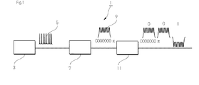
図1は,特開2001−177565号公報に開示された送信機を示すブロック図である。図1に示されるようにこの送信機1は,パルス光源3と,位相変調器などのコード部7と,強度変調器などの変調部9とを有する。そして,パルス光源3から出力されたコヒーレントなパルス光5が,コード部7によりチップ数N(図1では8)の光チップパルスに分割される。各チップパルスは,中心波長がλであり,“0”または“π”の位相情報が付加される。これによりアドレス情報が,光パルス列にマッピングされる。そして,変調部9は,パケット用データにしたがって光パルス列を変調する。これにより,データ情報が変調情報として付加される。
FIG. 1 is a block diagram showing a transmitter disclosed in Japanese Patent Laid-Open No. 2001-177565. As shown in FIG. 1, the
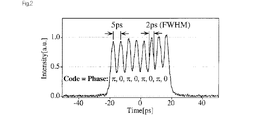
図2は,特開2001−177565号公報に開示されたパルス列を示す図である。図2に示されるように,この公報に開示された方法では,チップが“0”または“π”という位相情報により符号化されている。このためコードサイズが限られている。また,限られたコードサイズで符号化を行うため,相関特性に限界がある。さらに,符号化方式が固定され,容易に複号化できるため,傍受される恐れがある。 FIG. 2 is a diagram showing a pulse train disclosed in Japanese Patent Laid-Open No. 2001-177565. As shown in FIG. 2, in the method disclosed in this publication, a chip is encoded with phase information of “0” or “π”. For this reason, the code size is limited. In addition, since the encoding is performed with a limited code size, the correlation characteristics are limited. Furthermore, since the encoding method is fixed and can be easily decoded, it may be intercepted.
特開2007−096476号公報には,光符号分割多重アクセスシステムが開示されている。このシステムでは,ビットごとに位相変調を行い符号化する。しかしながら,ビットを構成するチップについては,位相変調を施していない。
本発明は,コードサイズを増加でき,相関特性を向上できる光情報通信システムを提供することを目的とする。 An object of the present invention is to provide an optical information communication system that can increase the code size and improve the correlation characteristics.
また,本発明は,安全性の高い光情報通信を行うことができる光情報通信システムを提供することを上記とは別の目的とする。 Another object of the present invention is to provide an optical information communication system capable of performing highly secure optical information communication.
本発明は,コードを構成する複数の時間分割された光チップパルスが,それぞれ,波長及び位相によりマッピングされた情報を有する。これにより,コードサイズを大幅に増加でき,相関特性を向上できる。また迅速に符号化形式を変化させることができるので,ビットごとに符号化形式を変化させることができ,安全性の高い情報通信を行うことができる。 The present invention has information in which a plurality of time-divided optical chip pulses constituting a code are mapped by wavelength and phase, respectively. This can greatly increase the code size and improve the correlation characteristics. Also, since the encoding format can be changed quickly, the encoding format can be changed bit by bit, and highly secure information communication can be performed.
本発明は,コードを構成する複数の時間分割された光チップパルスが,それぞれ,波長及び位相によりマッピングされた情報を有する。これにより,コードサイズを大幅に増加でき,相関特性を向上できる。また迅速に符号化形式を変化させることができるので,ビットごとに符号化形式を変化させることができ,安全性の高い情報通信を行うことができる。 The present invention has information in which a plurality of time-divided optical chip pulses constituting a code are mapped by wavelength and phase, respectively. This can greatly increase the code size and improve the correlation characteristics. Also, since the encoding format can be changed quickly, the encoding format can be changed bit by bit, and highly secure information communication can be performed.
以下,図面を用いて,本発明の実施の形態を説明する。図3は,本発明の光情報通信システム用送信機のブロック図である。図3に示されるように,本発明の光情報通信システム用送信機21は,パルス光源23,コード部27,及び変調部31を有する。本発明は,光符号分割多重アクセス(OCDMA)における公知の構成を適宜修正して用いることができる。
Hereinafter, embodiments of the present invention will be described with reference to the drawings. FIG. 3 is a block diagram of a transmitter for an optical information communication system according to the present invention. As shown in FIG. 3, the optical information
パルス光源23は,コヒーレントなパルス光25を得るものである。パルス光源として,OCDMAにおいて用いられるパルス光源を用いることができる。
The
本発明の光情報通信システム用送信機では,パルス光源23からコヒーレントなパルス光25が出力される。
In the transmitter for an optical information communication system of the present invention, coherent
コード部は,アドレスに相当するコード情報を形成するための装置である。通常のOCDMA用符号器では,図2に示されるようにチップパルスごとに位相情報を付加する。よって,従来のOCDMA用符号器では,位相変調器が存在すれば十分であった。本発明では,コード情報に位相情報のみならず波長情報も持たせる。このため,本発明のコード部は,分波・波長変調部33,位相変調部35及び合波部37を含む。
The code part is a device for forming code information corresponding to an address. In a normal OCDMA encoder, phase information is added for each chip pulse as shown in FIG. Therefore, it is sufficient for the conventional OCDMA encoder to have a phase modulator. In the present invention, the code information has not only phase information but also wavelength information. For this reason, the code unit of the present invention includes a demultiplexing / wavelength modulation unit 33, a
分波・波長変調部33は,パルス光を分波し,チップ数N(ただし,Nは2以上の整数)の光チップパルスを得るものである。分波・波長変調部33は,N個の光チップパルスのそれぞれに,波長変調を施す。分波・波長変調部の例は,第1のファイバブラッググレーティング(FBG)があげられる。分波・波長変調部33は,パルス光を分波して所定の時間間隔を与えて,それぞれの分波された光の波長をシフトさせ,それらの光を合波することができるものであれば,FBGを用いないものであっても良い。 The demultiplexing / wavelength modulation unit 33 demultiplexes the pulsed light and obtains an optical chip pulse with N chips (where N is an integer of 2 or more). The demultiplexing / wavelength modulation unit 33 performs wavelength modulation on each of the N optical chip pulses. An example of the demultiplexing / wavelength modulation unit is a first fiber Bragg grating (FBG). The demultiplexing / wavelength modulation unit 33 demultiplexes the pulsed light and gives a predetermined time interval, shifts the wavelength of each demultiplexed light, and multiplexes the lights. For example, an FBG may not be used.
ファイバグレーティングとして,ユニフォームファイバグレーティング,チャープグレーティング,又はマルチセクショングレーティングを用いるものがあげられる。以下,FBGについて説明する。FBGは,たとえば,位相マスクを介して紫外線を照射し,そのコアの屈折率を所定のピッチで変化させることにより得ることができる。 Examples of the fiber grating include those using a uniform fiber grating, a chirped grating, or a multi-section grating. Hereinafter, FBG will be described. The FBG can be obtained, for example, by irradiating ultraviolet rays through a phase mask and changing the refractive index of the core at a predetermined pitch.
ユニフォームFBGは,グレーティングの周期・屈折率などが均一なFBGである。ユニフォームFBGは,メインの反射帯域(メインフローブ)の他に,メインローブの周辺に不要な反射帯域(サイドローブ)が複数生ずる場合がある。 The uniform FBG is an FBG having a uniform grating period and refractive index. The uniform FBG may have a plurality of unnecessary reflection bands (side lobes) around the main lobe in addition to the main reflection band (main flow).
チャープグレーティングは,FBGの長手方向に屈折率周期やグレーティングの周期を変化させたチャープドFBGである。チャープグレーティングにより,入力信号の波長に応じて,反射する位置を異ならせることができる。そして,グレーティング部位を長くした長いチャープドグレーティングを用いれば,反射帯域が広くなるという利点がある。 The chirped grating is a chirped FBG in which the refractive index period and the grating period are changed in the longitudinal direction of the FBG. With the chirped grating, the reflection position can be varied according to the wavelength of the input signal. If a long chirped grating with a long grating part is used, there is an advantage that the reflection band is widened.
マルチセクションFBGは,波長変化と反射点変化が離散的なFBGである。すなわち,ある範囲の波長成分の光信号は,ほぼ同じ反射点で反射するが,それと異なる範囲の波長成分は反射点が離散的に変化することとなる。 The multi-section FBG is an FBG in which wavelength changes and reflection point changes are discrete. That is, optical signals having a certain range of wavelength components are reflected at substantially the same reflection point, but the reflection points of wavelength components in a different range are discretely changed.
なお,FBGは,スーパーストラクチャードFBGを用いても良い。このSSFBGは,光ファイバの導波方向に沿って複数の単位FBGが配列されて構成されたSSFBGである。SSFBGは,たとえば,光ファイバ形式のものである。光ファイバは,コアと,クラッドとを含む。コアは,光ファイバの光導波路である。そして,SSFBGは,コアの導波方向に沿って直列に配置された複数の単位FBGを含む。 Note that a superstructured FBG may be used as the FBG. This SSFBG is an SSFBG configured by arranging a plurality of unit FBGs along the waveguide direction of the optical fiber. The SSFBG is of an optical fiber type, for example. The optical fiber includes a core and a cladding. The core is an optical waveguide of an optical fiber. The SSFBG includes a plurality of unit FBGs arranged in series along the waveguide direction of the core.
なお,グレーティングのピッチは,対象とする光の波長などに応じて適切な間隔のものを用いればよく,たとえば,100nm〜1000nmがあげられ,300nm〜800nmでもよい。また,グレーティングのコアに対する屈折率差として,1×10−6〜1×10⁻²があげられ,1×10-5〜5×10⁻³でもよく,1×10−4〜1×10⁻³でもよい。 Note that the grating pitch may be an appropriate interval according to the wavelength of the target light, for example, 100 nm to 1000 nm, or 300 nm to 800 nm. Further, the refractive index difference with respect to the core of the grating, 1 × 10 -6 ~1 × 10 -2 , and the like, may also 1 × 10 -5 ~5 × 10 -3 , 1 × 10 -4 ~1 × 10 - 3 is also acceptable.
コード部に,パルス光源23から出力されたコヒーレントなパルス光25が入力される。このパルス光25は,分波・波長変調部33により分波され,チップ数N(ただし,Nは2以上の整数)の光チップパルスとされる。さらに,分波・波長変調部33は,N個の光チップパルスのそれぞれに,波長変調を施す。たとえば,あるパルス光が6つのチップパルスに分波される。そして,それぞれのチップパルスは,所定間隔の遅延を有している。さらに,それぞれのチップパルスは,波長が異なっており,たとえば,λ6λ4λ2λ5λ3λ1のように波長変調情報を有する。なお,この例では,FBGを用いたので,多数の種類の波長情報を各パルスに載せることができた。しかし,たとえば,公知のFSK変調器を用いるなど,2種類の波長変調情報を載せるものであっても良い。
Coherent pulsed light 25 output from the
位相変調部35は,分波・波長変調部から出力された波長変調を施されたN個の光チップパルスのそれぞれに,位相変調を施す。通常のOCDMA符号器では,N個の光チップパルスに位相変調(“0”又は“π”)を施す。本発明においても,公知のOCDMA符号器における位相変調器を用いることができる。同様に位相変調を施せばよい。なお,本発明では,たとえば,チップパルスに含まれる位相変調情報と波長変調情報をコード情報(アドレス情報)として用いる。そこで,アドレスに応じた符号化を行うことができるように,FBG(分波・波長変調部)を調整するほか,位相変調器に変調指令を出力する。
The
コード部33から位相変調部35へ波長変調が施されたチップ列(例λ6λ4λ2λ5λ3λ1)が入力される。このチップ列に含まれるそれぞれのパルスに位相変調を施す。図3の例では,“π00000”の位相変調を施す。なお,本発明においては,位相変調の例として,0又はπを用いた2値位相変調(BPSK)のほかに,4値位相変調(QPSK),8値位相変調(OPSK),16値位相変調,32値位相変調などさまざまな位相変調を採用できる。
A chip sequence (for example, λ 6 λ 4 λ 2 λ 5 λ 3 λ 1 ) subjected to wavelength modulation is input from the code unit 33 to the
合波部37は,位相変調部から出力されたN個の光チップパルスを合波する。合波部も公知のOCDMA符号器において用いられる装置を適宜採用することができる。分波・波長変調部がFBGを含むものであった場合,合波部もFBGを含むものが好ましい。具体的に説明すると,合波部は,第1のファイバブラッググレーティングに対応したグレーティングを有する第2のファイバブラッググレーティングを含むものが好ましい。
The multiplexing
コード部で位相変調が施されたチップ列は,合波部に入力される。そして,合波部で合わさる。これにより,各光チップパルスが位相変調情報と波長変調情報を持つパルス列29が得られる。
The chip sequence that has undergone phase modulation in the code part is input to the multiplexing part. Then, they are combined at the multiplexing part. Thereby, a
変調器31は,送信すべきデータに関する情報を前記パルス列に載せるために,パルス列29ごとに,データに関する情報に基づいて所定の変調を施すための装置である。変調器31として,OCDMA符号器における公知の変調器を用いることができる。
The
図4は,実施例1で用いたセットアップのブロック図である。モード同期レーザーダイオード(MLLD)とニオブ酸リチウム基板上の強度変調器(LN−IM)を用いて,1.25GHzの繰り返しレートにて,約1550nmに中心波長を有する1.5psの光パルス列を生成した。この光パルス列は,8チップのチャープドFBG(CFBG)により分波され,20GHzのニオブ酸リチウム基板上の位相変調器(LN−PM)により変調が施された。変調は,繰り返し周期が1.25GHzで,チップごとに50psのバイナリー位相シフト変調(BPSK)であった。合波器は,別のCFBGを用いても良いが,本実施例では,位相変調器からの出力をCFBGの裏側から入力することで代用した。CFBGの分散スロープ(dispersion slope)は,約65ps/nmであった。 FIG. 4 is a block diagram of the setup used in the first embodiment. Using a mode-locked laser diode (MLLD) and an intensity modulator (LN-IM) on a lithium niobate substrate, a 1.5 ps optical pulse train with a center wavelength of about 1550 nm is generated at a repetition rate of 1.25 GHz. did. This optical pulse train was demultiplexed by an 8-chip chirped FBG (CFBG) and modulated by a phase modulator (LN-PM) on a 20 GHz lithium niobate substrate. The modulation was binary phase shift modulation (BPSK) with a repetition period of 1.25 GHz and 50 ps per chip. As the multiplexer, another CFBG may be used, but in this embodiment, the output from the phase modulator is substituted from the back side of the CFBG. The dispersion slope of CFBG was about 65 ps / nm.
MLLD及びLN−IMで光パルスを得た。具体的には,MLLDで10GHzのパルス光を得て,パルス間隔をLN−IMで調整した。サーキュレータを経たパルス光を,2次元エンコーダとして機能するファーバーグレーティング(FBG)に導入した。FBGに入力されたパルス光は,複数の地点で折り返し,等間隔に時間遅延が与えられるとともに,異なる波長とされる。これにより,異なる波長を有する複数のチップパルスを得た。 Light pulses were obtained with MLLD and LN-IM. Specifically, pulse light of 10 GHz was obtained by MLLD, and the pulse interval was adjusted by LN-IM. The pulsed light that passed through the circulator was introduced into the Farberg Rating (FBG) that functions as a two-dimensional encoder. The pulsed light input to the FBG is turned back at a plurality of points, is given a time delay at equal intervals, and has different wavelengths. As a result, a plurality of chip pulses having different wavelengths were obtained.
次に,LN−PMにより位相変調を施した。この際,チップパルスの集合であるビットにいて位相変調が施されるほか,それぞれのチップパルスについても位相変調を施した。つまり,この例では位相変調器をひとつ用いて,チップに位相変調情報を載せるとともに,ビットについても位相変調を施した。 Next, phase modulation was performed by LN-PM. At this time, the phase modulation was applied to the bits that are a set of chip pulses, and the phase modulation was also applied to each chip pulse. In other words, in this example, one phase modulator was used to place phase modulation information on the chip, and phase modulation was also applied to the bits.
位相変調器を経たチップパルスを,サーキュレータを経てFGBに入力した。この際,先に入力したのとは逆側から入力した。FBGから戻ったチップパルスは,サーキュレータを経て出力される。なお,この実施例では,出力されたチップパルスをさらにLN−IMで強度変調した。このLN−IMは,フィルタとして機能するものである。 The chip pulse that passed through the phase modulator was input to the FGB via the circulator. At this time, it was input from the opposite side of the previous input. The chip pulse returned from the FBG is output through the circulator. In this embodiment, the output chip pulse is further intensity-modulated with LN-IM. This LN-IM functions as a filter.
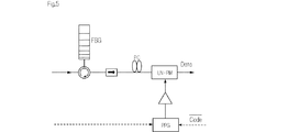
図5は,本実施例で用いた受信機(複号器)を示すブロック図である。複号部の信号制御部(図では,実験のためパルスパターン発生器が用いられている)には,符号部からの同期信号が送られる。このため,ビットごとに符号化様式(と複号化様式)を変えることができる。これにより,光信号を傍受された場合も容易に複号化できない。 FIG. 5 is a block diagram showing a receiver (decoder) used in this embodiment. A synchronization signal from the encoding unit is sent to the signal control unit of the decoding unit (in the figure, a pulse pattern generator is used for experiments). For this reason, the encoding format (and decoding format) can be changed for each bit. As a result, even if an optical signal is intercepted, it cannot be easily decoded.
本発明の光情報通信システムの性能評価
図6Aは,実施例2における2次元コードパターンを示す。この例では,時間が遅いチップパルスになるにしたがって,波長が大きくなるように変調を施した。すなわち,2次元コードパターンのうち波長によるパターンが(λ1λ2λ3λ4λ5)となるように符号化した。図6B及び図6Cは,符号器による応答を示すグラフである。図6Bは,波長変調による符号パターンを示す。図6Bに示されるように1nmの波長間隔で変調した。図6Cは,この例における時間とチップパルスの波長との関係を示すグラフである。
Performance Evaluation of Optical Information Communication System of the Present Invention FIG. 6A shows a two-dimensional code pattern in the second embodiment. In this example, modulation is performed so that the wavelength increases as the chip pulse becomes slower. That is, the two-dimensional code pattern is encoded so that the pattern by wavelength becomes (λ 1 λ 2 λ 3 λ 4 λ 5 ). 6B and 6C are graphs showing the response by the encoder. FIG. 6B shows a code pattern by wavelength modulation. Modulation was performed at a wavelength interval of 1 nm as shown in FIG. 6B. FIG. 6C is a graph showing the relationship between the time and the wavelength of the chip pulse in this example.
図6Dは,符号化後の波形を示す。図6Dにおいて縦軸は強度,横軸は時間(1メモリ100ピコ秒)である。図6Eは,符号化後のスペクトルを示す。図6Eにおいて縦軸は強度,横軸は波長(nm)を示す。この例では,位相変調器(PM)をチップごとに10GHzで駆動し,1.25GHzの繰り返しレートの2次元スペクトル位相符号化パターンを用いた5チップのBPSK(2値位相シフト変調)を行うことで,コヒーレントな2次元スペクトル位相符号化(SPE:spectral phase coding)を得た。なお,この例では,簡単のため全てのSPEパターンの位相を“0”とした。 FIG. 6D shows the waveform after encoding. In FIG. 6D, the vertical axis represents intensity, and the horizontal axis represents time (one memory 100 picoseconds). FIG. 6E shows the spectrum after encoding. In FIG. 6E, the vertical axis represents intensity and the horizontal axis represents wavelength (nm). In this example, the phase modulator (PM) is driven at 10 GHz for each chip, and 5-chip BPSK (binary phase shift modulation) is performed using a two-dimensional spectral phase encoding pattern with a repetition rate of 1.25 GHz. Thus, a coherent two-dimensional spectral phase coding (SPE) was obtained. In this example, the phases of all SPE patterns are set to “0” for simplicity.
本発明の光情報通信システムの性能評価
図7Aは,実施例3における2次元コードパターンを示す。すなわち,2次元コードパターンのうち波長によるパターンが(λ1λ4λ2λ5λ3)となるように符号化した。図7B及び図7Cは,符号器による応答を示すグラフである。図7Bは,波長変調による符号パターンを示す。図7Bに示されるように1nmの波長間隔で変調した。図7Cは,この例における時間とチップパルスの波長との関係を示すグラフである。
Performance Evaluation of Optical Information Communication System of the Present Invention FIG. 7A shows a two-dimensional code pattern in the third embodiment. That is, the two-dimensional code pattern was encoded so that the pattern by wavelength becomes (λ 1 λ 4 λ 2 λ 5 λ 3 ). 7B and 7C are graphs showing the response by the encoder. FIG. 7B shows a code pattern by wavelength modulation. Modulation was performed at a wavelength interval of 1 nm as shown in FIG. 7B. FIG. 7C is a graph showing the relationship between the time and the wavelength of the chip pulse in this example.
図7Dは,符号化後の波形を示す。図7Dにおいて縦軸は強度,横軸は時間(1メモリ100ピコ秒)である。図7Eは,符号化後のスペクトルを示す。図7Eにおいて縦軸は強度,横軸は波長(nm)を示す。この例では,位相変調器(PM)をチップごとに10GHzで駆動し,1.25GHzの繰り返しレートの2次元スペクトル位相符号化パターンを用いた5チップのBPSK(2値位相シフト変調)を行うことで,コヒーレントな2次元スペクトル位相符号化(SPE:spectral phase coding)を得た。なお,この例では,簡単のため全てのSPEパターンの位相を“0”とした。 FIG. 7D shows the waveform after encoding. In FIG. 7D, the vertical axis represents intensity, and the horizontal axis represents time (one memory 100 picoseconds). FIG. 7E shows the spectrum after encoding. In FIG. 7E, the vertical axis represents intensity and the horizontal axis represents wavelength (nm). In this example, the phase modulator (PM) is driven at 10 GHz for each chip, and 5-chip BPSK (binary phase shift modulation) is performed using a two-dimensional spectral phase encoding pattern with a repetition rate of 1.25 GHz. Thus, a coherent two-dimensional spectral phase coding (SPE) was obtained. In this example, the phases of all SPE patterns are set to “0” for simplicity.
本発明の光情報通信システムの性能評価
図8Aは,実施例4における2次元コードパターンを示す。すなわち,2次元コードパターンのうち波長によるパターンが(λ1λ3λ5λ2λ4)となるように符号化した。図8B及び図8Cは,符号器による応答を示すグラフである。図8Bは,波長変調による符号パターンを示す。図8Bに示されるように1nmの波長間隔で変調した。図8Cは,この例における時間とチップパルスの波長との関係を示すグラフである。
FIG. 8A shows a two-dimensional code pattern in the fourth embodiment. That is, the two-dimensional code pattern was encoded so that the pattern by wavelength becomes (λ 1 λ 3 λ 5 λ 2 λ 4 ). 8B and 8C are graphs showing responses by the encoder. FIG. 8B shows a code pattern by wavelength modulation. Modulation was performed at a wavelength interval of 1 nm as shown in FIG. 8B. FIG. 8C is a graph showing the relationship between the time and the wavelength of the chip pulse in this example.
図8Dは,符号化後の波形を示す。図8Dにおいて縦軸は強度,横軸は時間(1メモリ100ピコ秒)である。図8Eは,符号化後のスペクトルを示す。図8Eにおいて縦軸は強度,横軸は波長(nm)を示す。この例では,位相変調器(PM)をチップごとに10GHzで駆動し,1.25GHzの繰り返しレートの2次元スペクトル位相符号化パターンを用いた5チップのBPSK(2値位相シフト変調)を行うことで,コヒーレントな2次元スペクトル位相符号化(SPE:spectral phase coding)を得た。なお,この例では,簡単のため全てのSPEパターンの位相を“0”とした。 FIG. 8D shows the waveform after encoding. In FIG. 8D, the vertical axis represents intensity, and the horizontal axis represents time (1 memory 100 picoseconds). FIG. 8E shows the spectrum after encoding. In FIG. 8E, the vertical axis represents intensity, and the horizontal axis represents wavelength (nm). In this example, the phase modulator (PM) is driven at 10 GHz for each chip, and 5-chip BPSK (binary phase shift modulation) is performed using a two-dimensional spectral phase encoding pattern with a repetition rate of 1.25 GHz. Thus, a coherent two-dimensional spectral phase coding (SPE) was obtained. In this example, the phase of all SPE patterns is set to “0” for simplicity.
本発明の光情報通信システムの性能評価
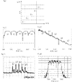
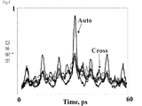
図9は,自己相関スペクトルと,相互相関スペクトルを示す観測されたグラフである。自己相関スペクトル(すなわち,符号様式が一致した場合)は高いピークを有しており,相互相関スペクトル(すなわち,符号様式が一致しない場合)は高いピークが存在しない。よって,本発明の光情報通信システムを用いて,効果的に符号化及び複号化できることがわかる。
FIG. 9 is an observed graph showing an autocorrelation spectrum and a cross-correlation spectrum. The autocorrelation spectrum (that is, when the code formats match) has a high peak, and the cross-correlation spectrum (that is, when the code formats do not match) does not have a high peak. Therefore, it can be seen that the optical information communication system of the present invention can be used for effective encoding and decoding.
本発明は光情報通信などの分野で利用されうる。 The present invention can be used in fields such as optical information communication.
1 送信機
3 パルス光源
5 パルス光
7 コード部
9 変調部
21 光情報通信システム用送信機
23 パルス光源
25 パルス光
27 コード部
29 パルス列
31 変調部
33 分波・波長変調部
35 位相変調部
37 合波部
DESCRIPTION OF
Claims (5)
前記コード部には,
前記パルス光源(23)から出力されたコヒーレントなパルス光(25)が入力され,
前記コード部は,
分波・波長変調部(33),位相変調部(35)及び合波部(37)を含み,
前記分波・波長変調部(33)は,
前記パルス光を分波し,チップ数N(ただし,Nは2以上の整数)の光チップパルスを得るものであって,
前記N個の光チップパルスのそれぞれに,波長変調を施し,
前記位相変調部(35)は,
前記分波・波長変調部から出力された
波長変調を施されたN個の光チップパルスのそれぞれに,位相変調を施し,
前記合波部(37)は,
前記位相変調部から出力されたN個の光チップパルスを合波し,これにより,各光チップパルスが位相変調情報と波長変調情報を持つパルス列(29)を得,
前記変調器(31)は,
送信すべきデータに関する情報を前記パルス列に載せるために,前記パルス列(29)ごとに,前記データに関する情報に基づいて所定の変調を施す,
光情報通信システム用送信機。
A transmitter (21) for an optical information communication system having a pulse light source (23), a code part (27), and a modulation part (31),
In the cord part,
Coherent pulse light (25) output from the pulse light source (23) is input,
The code part is
Including a demultiplexing / wavelength modulation section (33), a phase modulation section (35) and a multiplexing section (37);
The demultiplexing / wavelength modulation section (33)
Demultiplexing the pulsed light to obtain an optical chip pulse of N chips (where N is an integer of 2 or more),
Wavelength modulation is applied to each of the N optical chip pulses,
The phase modulation section (35)
Phase modulation is performed on each of the N optical chip pulses subjected to wavelength modulation output from the demultiplexing / wavelength modulation unit,
The multiplexing unit (37)
N optical chip pulses output from the phase modulation unit are multiplexed, thereby obtaining a pulse train (29) in which each optical chip pulse has phase modulation information and wavelength modulation information,
The modulator (31)
In order to put information on data to be transmitted on the pulse train, for each pulse train (29), a predetermined modulation is performed based on the information on the data.
Transmitter for optical information communication system.
ひとつの位相変調器である,
請求項1に記載の光情報通信システム用送信機。
The phase modulation unit (35) and the modulator (31) are:
One phase modulator,
The transmitter for an optical information communication system according to claim 1.
第1のファイバブラッググレーティングである,
請求項1に記載の光情報通信システム用送信機。
The demultiplexing / wavelength modulation unit is:
A first fiber Bragg grating,
The transmitter for an optical information communication system according to claim 1.
請求項3に記載の光情報通信システム用送信機。
The multiplexing unit includes a second fiber Bragg grating having a grating corresponding to the first fiber Bragg grating;
The transmitter for an optical information communication system according to claim 3.
Priority Applications (1)
| Application Number | Priority Date | Filing Date | Title |
|---|---|---|---|
| JP2008233961A JP5262481B2 (en) | 2008-09-11 | 2008-09-11 | Optical information communication system using optical code having phase information |
Applications Claiming Priority (1)
| Application Number | Priority Date | Filing Date | Title |
|---|---|---|---|
| JP2008233961A JP5262481B2 (en) | 2008-09-11 | 2008-09-11 | Optical information communication system using optical code having phase information |
Publications (2)
| Publication Number | Publication Date |
|---|---|
| JP2010068352A true JP2010068352A (en) | 2010-03-25 |
| JP5262481B2 JP5262481B2 (en) | 2013-08-14 |
Family
ID=42193518
Family Applications (1)
| Application Number | Title | Priority Date | Filing Date |
|---|---|---|---|
| JP2008233961A Expired - Fee Related JP5262481B2 (en) | 2008-09-11 | 2008-09-11 | Optical information communication system using optical code having phase information |
Country Status (1)
| Country | Link |
|---|---|
| JP (1) | JP5262481B2 (en) |
Citations (5)
| Publication number | Priority date | Publication date | Assignee | Title |
|---|---|---|---|---|
| JP2001177565A (en) * | 1999-12-15 | 2001-06-29 | Communications Research Laboratory Mphpt | Packet routing method of photonic network and packet router for photonic network |
| JP2005020459A (en) * | 2003-06-26 | 2005-01-20 | Oki Electric Ind Co Ltd | Optical code division multiplex transmission method and optical code division multiplex transmitting apparatus |
| JP2006060658A (en) * | 2004-08-23 | 2006-03-02 | Oki Electric Ind Co Ltd | Method and system for optical code multiplex communication coding device, coding device, and decoding device |
| JP2006238118A (en) * | 2005-02-25 | 2006-09-07 | Oki Electric Ind Co Ltd | Method and apparatus for optical division multiplex sending-receiving |
| JP2007329541A (en) * | 2006-06-06 | 2007-12-20 | Oki Electric Ind Co Ltd | Optical coder, optical decoder, and optical code division multiplexing transmission/reception apparatus |
-
2008
- 2008-09-11 JP JP2008233961A patent/JP5262481B2/en not_active Expired - Fee Related
Patent Citations (5)
| Publication number | Priority date | Publication date | Assignee | Title |
|---|---|---|---|---|
| JP2001177565A (en) * | 1999-12-15 | 2001-06-29 | Communications Research Laboratory Mphpt | Packet routing method of photonic network and packet router for photonic network |
| JP2005020459A (en) * | 2003-06-26 | 2005-01-20 | Oki Electric Ind Co Ltd | Optical code division multiplex transmission method and optical code division multiplex transmitting apparatus |
| JP2006060658A (en) * | 2004-08-23 | 2006-03-02 | Oki Electric Ind Co Ltd | Method and system for optical code multiplex communication coding device, coding device, and decoding device |
| JP2006238118A (en) * | 2005-02-25 | 2006-09-07 | Oki Electric Ind Co Ltd | Method and apparatus for optical division multiplex sending-receiving |
| JP2007329541A (en) * | 2006-06-06 | 2007-12-20 | Oki Electric Ind Co Ltd | Optical coder, optical decoder, and optical code division multiplexing transmission/reception apparatus |
Non-Patent Citations (2)
| Title |
|---|
| JPN6012059628; Nasaruddin, et al.: 'Design of Reconfigurable Multiweight Wavelength-Time Optical Codes for Secure Multimedia Optical CDM' IEEE International Conference on Communications, 2008. ICC '08. , 20080519, pages.5437-5442, IEEE * |
| JPN6012059629; Santiago Tainta, et al.: 'Spectrally Efficient Phase Encoded Optical CDMA System in Time Domain' Conference on Optical Fiber communication/National Fiber Optic Engineers Conference, 2008. OFC/NFOEC JThA30.pdf, 20080224, pages.1-3, IEEE * |
Also Published As
| Publication number | Publication date |
|---|---|
| JP5262481B2 (en) | 2013-08-14 |
Similar Documents
| Publication | Publication Date | Title |
|---|---|---|
| Teh et al. | A comparative study of the performance of seven-and 63-chip optical code-division multiple-access encoders and decoders based on superstructured fiber Bragg gratings | |
| JP4561403B2 (en) | Optical division multiplexing transmission / reception method and optical division multiplexing transmission / reception apparatus | |
| US7702240B2 (en) | Optical multiplex communication system and delay quantity adjustment method | |
| JP2010114488A (en) | Optical code division multiplex signal generator | |
| JP2010200244A (en) | Method of decoding code, optical pulse time spreading device, optical branch insertion device, and optical communication system | |
| JP2006319843A (en) | Optical pulse time spreading device | |
| JP3038378B1 (en) | Optical code division multiplex communication system | |
| US7983561B2 (en) | Optical pulse time spreading device | |
| CA2376858C (en) | Communication systems and apparatus with synchronous orthogonal coding | |
| JP5262481B2 (en) | Optical information communication system using optical code having phase information | |
| Matsushima et al. | Experimental demonstration of performance improvement of 127-chip SSFBG en/decoder using apodization technique | |
| JP2009200733A (en) | Optical code division multiplex access system | |
| JP4649582B2 (en) | Optical code division multiple packet communication system | |
| JP2011182052A (en) | Optical pulse time spreading device | |
| JP2004170734A (en) | Optical code division multiplex communication apparatus | |
| US8200089B2 (en) | Optical pulse time spreading apparatus and optical multiplex transmitting system with multiplexed channels and S/N ratio increased | |
| JP5228646B2 (en) | Optical pulse time spreader | |
| JP4622785B2 (en) | Optical code division multiplexing transmitter | |
| JP2007005888A (en) | Optical waveguide device and optical code division multiplex communication system | |
| JP5471694B2 (en) | Optical signal channel division multiplexing communication method and optical signal channel division multiplexing communication apparatus | |
| Minato et al. | Demonstration of 10 Gbit/s-based time-spreading and wavelength-hopping optical-code-division-multiplexing using fiber-Bragg-grating en/decoder | |
| JP2004341307A (en) | Optical encoder and optical decoder | |
| Galli et al. | Novel results on the coexistence of spectrally phase-encoded OCDMA and DWDM | |
| JP2004228840A (en) | Optical encoded signal generator and optical code division multiplexer | |
| JP2004170733A (en) | Optical signal transducer, optical encoder, decoder, and optical code division multiplex communication apparatus |
Legal Events
| Date | Code | Title | Description |
|---|---|---|---|
| A621 | Written request for application examination |
Free format text: JAPANESE INTERMEDIATE CODE: A621 Effective date: 20110902 |
|
| A977 | Report on retrieval |
Free format text: JAPANESE INTERMEDIATE CODE: A971007 Effective date: 20121107 |
|
| A131 | Notification of reasons for refusal |
Free format text: JAPANESE INTERMEDIATE CODE: A131 Effective date: 20121120 |
|
| A521 | Written amendment |
Free format text: JAPANESE INTERMEDIATE CODE: A523 Effective date: 20130104 |
|
| TRDD | Decision of grant or rejection written | ||
| A01 | Written decision to grant a patent or to grant a registration (utility model) |
Free format text: JAPANESE INTERMEDIATE CODE: A01 Effective date: 20130409 |
|
| A61 | First payment of annual fees (during grant procedure) |
Free format text: JAPANESE INTERMEDIATE CODE: A61 Effective date: 20130415 |
|
| R150 | Certificate of patent or registration of utility model |
Free format text: JAPANESE INTERMEDIATE CODE: R150 Ref document number: 5262481 Country of ref document: JP Free format text: JAPANESE INTERMEDIATE CODE: R150 |
|
| S533 | Written request for registration of change of name |
Free format text: JAPANESE INTERMEDIATE CODE: R313533 |
|
| R350 | Written notification of registration of transfer |
Free format text: JAPANESE INTERMEDIATE CODE: R350 |
|
| R250 | Receipt of annual fees |
Free format text: JAPANESE INTERMEDIATE CODE: R250 |
|
| R250 | Receipt of annual fees |
Free format text: JAPANESE INTERMEDIATE CODE: R250 |
|
| R250 | Receipt of annual fees |
Free format text: JAPANESE INTERMEDIATE CODE: R250 |
|
| LAPS | Cancellation because of no payment of annual fees |