JP2010063243A - Power supply circuit, its control method and electronic equipment - Google Patents
Power supply circuit, its control method and electronic equipment Download PDFInfo
- Publication number
- JP2010063243A JP2010063243A JP2008225165A JP2008225165A JP2010063243A JP 2010063243 A JP2010063243 A JP 2010063243A JP 2008225165 A JP2008225165 A JP 2008225165A JP 2008225165 A JP2008225165 A JP 2008225165A JP 2010063243 A JP2010063243 A JP 2010063243A
- Authority
- JP
- Japan
- Prior art keywords
- voltage
- power supply
- input voltage
- transformer
- input
- Prior art date
- Legal status (The legal status is an assumption and is not a legal conclusion. Google has not performed a legal analysis and makes no representation as to the accuracy of the status listed.)
- Pending
Links
- 238000000034 method Methods 0.000 title claims abstract description 13
- 238000012544 monitoring process Methods 0.000 claims description 35
- 238000004146 energy storage Methods 0.000 claims description 16
- 230000005284 excitation Effects 0.000 claims description 16
- 238000006243 chemical reaction Methods 0.000 claims description 3
- 238000001514 detection method Methods 0.000 claims description 2
- 238000007599 discharging Methods 0.000 claims description 2
- 230000005856 abnormality Effects 0.000 abstract description 15
- 239000003990 capacitor Substances 0.000 description 59
- 238000004804 winding Methods 0.000 description 41
- 238000010586 diagram Methods 0.000 description 12
- 230000007423 decrease Effects 0.000 description 5
- 230000002159 abnormal effect Effects 0.000 description 4
- 238000009499 grossing Methods 0.000 description 4
- 238000004891 communication Methods 0.000 description 3
- 238000005516 engineering process Methods 0.000 description 2
- 238000012937 correction Methods 0.000 description 1
- 238000013461 design Methods 0.000 description 1
- 230000009977 dual effect Effects 0.000 description 1
- 230000005669 field effect Effects 0.000 description 1
- 230000002265 prevention Effects 0.000 description 1
- 230000002035 prolonged effect Effects 0.000 description 1
Images

Landscapes
- Dc-Dc Converters (AREA)
Abstract
Description
本発明は、電源回路及びその制御方法並びに電子機器に関する。特に、本発明は、入力される電源電圧に異常が発生した場合であっても、適正な出力電圧を供給することができる電源回路及びその制御方法、並びに、該電源回路を備えた電子機器に関する。 The present invention relates to a power supply circuit, a control method thereof, and an electronic device. In particular, the present invention relates to a power supply circuit that can supply an appropriate output voltage even when an abnormality occurs in the input power supply voltage, a control method thereof, and an electronic device including the power supply circuit. .
各種の電子機器の安定化電源として、スイッチング電源回路が知られている。スイッチング電源回路は、電力を変換・調整するための変圧器やスイッチング素子を備え、当該スイッチング素子をオン、オフ動作することにより、所定の入力電圧から所望の出力電圧を生成するものである。例えば特許文献1や特許文献2には、入力電圧を供給する給電線間に接続され、該入力電圧を平滑化する入力コンデンサや、所定のタイミングで変圧器の一次巻線に並列に接続されるコンデンサを備えたスイッチング電源回路が開示されている。 A switching power supply circuit is known as a stabilized power supply for various electronic devices. The switching power supply circuit includes a transformer and a switching element for converting and adjusting electric power, and generates a desired output voltage from a predetermined input voltage by turning on and off the switching element. For example, in Patent Document 1 and Patent Document 2, an input capacitor connected between power supply lines for supplying an input voltage is connected in parallel to an input capacitor for smoothing the input voltage or a primary winding of a transformer at a predetermined timing. A switching power supply circuit having a capacitor is disclosed.
このようなスイッチング電源回路における動作は、まず、正常(通常)動作時には、変圧器の磁性体に蓄積された励磁エネルギーに基づいて所定の出力電圧を生成して電子機器に供給しつつ、上記コンデンサに励磁エネルギーに応じたエネルギーを蓄積する。すなわち、スイッチング電源回路は、上記のスイッチング素子をオン、オフ動作(スイッチング)する毎に、変圧器の磁性体を励磁するエネルギーと、変圧器や接続配線のインダクタンスに蓄えられるエネルギーを入力側から取り入れる。これらのエネルギーは、変圧器の磁性体を磁気リセットする際に上記コンデンサやスイッチング素子のキャパシタンスに充電され、磁気リセットの完了後に、変圧器の一次側へ回生される。スイッチング電源回路は、このような動作を繰り返すことにより、変圧器の二次側から所定の電圧を出力しつつ、コンデンサを充電する。 In such a switching power supply circuit, first, during normal (normal) operation, a predetermined output voltage is generated based on the excitation energy accumulated in the magnetic body of the transformer and supplied to the electronic device, while the capacitor is The energy corresponding to the excitation energy is stored. That is, the switching power supply circuit takes in the energy for exciting the magnetic body of the transformer and the energy stored in the inductance of the transformer and the connection wiring from the input side every time the switching element is turned on / off (switching). . These energies are charged to the capacitances of the capacitors and switching elements when the magnetic body of the transformer is magnetically reset, and are regenerated to the primary side of the transformer after the magnetic reset is completed. The switching power supply circuit repeats such an operation to charge the capacitor while outputting a predetermined voltage from the secondary side of the transformer.
そして、入力電圧の瞬時低下や瞬時遮断等の異常が発生して、正常動作範囲よりも低下した場合には、スイッチング電源回路は、上記コンデンサに蓄積したエネルギーを変圧器の一次側に供給することにより、出力電圧を継続して生成する。 When an abnormality such as an instantaneous drop in the input voltage or an instantaneous interruption occurs and falls below the normal operating range, the switching power supply circuit supplies the energy stored in the capacitor to the primary side of the transformer. Thus, the output voltage is continuously generated.
ここで、上記のようなスイッチング電源回路において、変圧器の磁性体を磁気リセットする時間や当該リセット電圧を調整するために、電圧クランプ回路を設けた構成も知られている。このようなスイッチング電源回路は、例えば特許文献3に開示されている。 Here, in the switching power supply circuit as described above, a configuration in which a voltage clamp circuit is provided in order to adjust the time for magnetic resetting the magnetic body of the transformer and the reset voltage is also known. Such a switching power supply circuit is disclosed in Patent Document 3, for example.
また、上記のようなスイッチング電源回路において、正常動作時にコンデンサに充電される電圧は、回路構成上、入力電圧と同等の電圧になる。そのため、入力電圧が電源回路の正常動作可能電圧の下限に近い場合、入力電圧に異常が発生した場合には、上記コンデンサからのエネルギーのみで出力電圧を安定的に供給できる時間(動作維持時間)を長くすることができない。そこで、スイッチング電源回路の動作維持時間を長くするために、昇圧回路を使用してコンデンサに充電する電圧を高くする構成が知られている。例えば特許文献4には、DC/DCコンバータ(直流−直流電圧変換器)の一次側に力率改善回路を備え、商用交流電源から生成される入力電圧よりも高い電圧を蓄電器(電解コンデンサ)に充電する構成を備えたスイッチング電源回路が開示されている。これにより、商用交流電源からの入力電圧の異常発生時に、蓄電器の充電電圧をDC/DCコンバータに入力することにより、出力電圧を安定的に供給できる時間を長くすることができる。 In the switching power supply circuit as described above, the voltage charged in the capacitor during normal operation is equivalent to the input voltage in terms of circuit configuration. Therefore, when the input voltage is close to the lower limit of the normal operating voltage of the power supply circuit, or when an abnormality occurs in the input voltage, the time during which the output voltage can be stably supplied only by the energy from the capacitor (operation maintaining time) Can not be lengthened. Therefore, in order to increase the operation maintaining time of the switching power supply circuit, a configuration is known in which the voltage charged in the capacitor is increased using a booster circuit. For example, in Patent Document 4, a power factor correction circuit is provided on the primary side of a DC / DC converter (DC-DC voltage converter), and a voltage higher than an input voltage generated from a commercial AC power supply is supplied to a capacitor (electrolytic capacitor). A switching power supply circuit having a configuration for charging is disclosed. As a result, when an abnormality occurs in the input voltage from the commercial AC power supply, it is possible to extend the time during which the output voltage can be stably supplied by inputting the charging voltage of the battery to the DC / DC converter.
ところで、スイッチング電源回路は、入力電圧を供給する電源に応じて、交流入力型と直流入力型に分類される。上述した各特許文献に開示されたスイッチング電源回路はいずれも、商用電源等から供給される交流電圧を入力電圧とする交流入力型に属している。これに対して、直流入力型のスイッチング電源回路は、バッテリ等で常にバックアップする構成を有しているため、入力電圧の瞬時低下に対応する規定はほとんど設けられておらず、それ故、入力電圧の低下に対応する技術に対してニーズは高くなかった。 By the way, the switching power supply circuit is classified into an AC input type and a DC input type according to the power supply that supplies the input voltage. Each of the switching power supply circuits disclosed in each of the patent documents described above belongs to an AC input type in which an AC voltage supplied from a commercial power supply or the like is used as an input voltage. On the other hand, since the DC input type switching power supply circuit has a configuration that always backs up with a battery or the like, there is almost no provision corresponding to an instantaneous drop in the input voltage. The need for technology that can cope with the decline was not high.
しかし、近年、直流入力型の電源回路においても、入力電圧の瞬時低下が生じた場合にも、安定的な出力電圧の維持を求める規定が設けられ、上記のような入力電圧の低下に対応する技術に対してニーズが急速に高まっている。 However, in recent years, even in a DC input type power supply circuit, even when an instantaneous drop in input voltage occurs, provisions for maintaining a stable output voltage are provided to cope with such a decrease in input voltage as described above. The need for technology is growing rapidly.
上述した各特許文献に記載されたスイッチング電源回路は、交流電圧を入力電圧とする交流入力型であるため、整流回路を備えている。そのため、入力電圧が正常動作範囲よりも低下した場合であっても、コンデンサに蓄積された電荷が入力側から外部に流出することはない。これに対して、バッテリ等からの直流電圧を入力電圧とする直流入力型のスイッチング電源回路においては、二重化入力用の逆流防止素子や、入力を開閉する素子を備えていないと、入力電圧が正常動作範囲よりも低下した場合、コンデンサに蓄積された電荷が入力側から外部へ流出してしまうという問題を有している。そのため、直流入力型のスイッチング電源回路においては、入力電圧に瞬時低下や瞬時遮断等の異常が発生した場合、出力電圧の安定的な供給動作を継続できないという問題を有していた。また、このような問題を防ぐためには、上記のような逆流防止用の素子や回路を設けなければならないが、その場合、回路規模が大きくなってしまうという問題を有していた。 Since the switching power supply circuit described in each patent document described above is an AC input type using an AC voltage as an input voltage, it includes a rectifier circuit. Therefore, even when the input voltage falls below the normal operating range, the charge accumulated in the capacitor does not flow out from the input side. On the other hand, in a DC input type switching power supply circuit that uses a DC voltage from a battery or the like as an input voltage, the input voltage is normal unless a backflow prevention element for dual input or an element for opening and closing the input are provided. When it falls below the operating range, there is a problem that the electric charge accumulated in the capacitor flows out from the input side to the outside. For this reason, the DC input type switching power supply circuit has a problem that when an abnormality such as an instantaneous drop or an instantaneous interruption occurs in the input voltage, the stable supply operation of the output voltage cannot be continued. Further, in order to prevent such a problem, it is necessary to provide the above-described elements and circuits for preventing backflow. In this case, however, there is a problem that the circuit scale becomes large.
なお、上記のような異常発生時に、出力電圧を安定的に供給できる時間を長くするための他の方策としては、変圧器の一次側に昇圧回路やその制御回路等を設け、入力電圧よりも高い電圧を生成してコンデンサへの充電電圧を高くする構成が考えられる。しかしながら、この場合においても、回路規模が大きくなってしまうという問題を有していた。 As another measure for increasing the time during which the output voltage can be stably supplied when an abnormality such as the above occurs, a booster circuit or its control circuit is provided on the primary side of the transformer, so that it is more than the input voltage. A configuration in which a high voltage is generated to increase the charging voltage to the capacitor is conceivable. However, even in this case, there is a problem that the circuit scale becomes large.
本発明の目的は、入力電圧に瞬時低下や瞬時遮断等の異常が発生した場合に、出力電圧の安定的な供給動作を長時間にわたり維持することができないという課題を解決する電源回路及びその制御方法、並びに、該電源回路を備えた電子機器を提供することにある。 An object of the present invention is to provide a power supply circuit that solves the problem that a stable supply operation of an output voltage cannot be maintained for a long time when an abnormality such as an instantaneous drop or instantaneous interruption occurs in the input voltage, and its control A method and an electronic device including the power supply circuit are provided.
本発明の電源回路は、入力電圧を出力電圧に変換する変圧器と、前記入力電圧が所定の電圧範囲内にある場合には、前記入力電圧を前記変圧器に供給するとともに、前記変圧器を励磁及び磁気リセットするエネルギーに基づいて、前記入力電圧よりも高い電圧を充電し、前記入力電圧が前記電圧範囲外にある場合には、前記充電された充電電圧に基づく電圧を、前記入力電圧として前記変圧器に供給する入力回路部と、を有している。 The power supply circuit of the present invention includes a transformer that converts an input voltage into an output voltage, and when the input voltage is within a predetermined voltage range, the input voltage is supplied to the transformer, and the transformer is Based on the energy for excitation and magnetic reset, a voltage higher than the input voltage is charged, and when the input voltage is outside the voltage range, the voltage based on the charged charge voltage is used as the input voltage. And an input circuit section for supplying to the transformer.
また、本発明の電源回路の制御方法は、変圧器に供給する入力電圧を検出し、該入力電圧が所定の電圧範囲内にあるか否かを監視するステップと、前記入力電圧を前記変圧器に供給するとともに、前記変圧器を励磁及び磁気リセットするエネルギーに基づいて、前記入力電圧よりも高い電圧を充電するステップと、前記入力電圧が所定の電圧範囲外にあると判定された場合に、前記充電された充電電圧に基づく電圧を、前記入力電圧として前記変圧器に供給するステップと、を含む。 The method for controlling a power supply circuit according to the present invention includes a step of detecting an input voltage supplied to a transformer and monitoring whether or not the input voltage is within a predetermined voltage range; And charging the voltage higher than the input voltage based on energy for exciting and magnetically resetting the transformer, and when it is determined that the input voltage is outside a predetermined voltage range, Supplying a voltage based on the charged charging voltage to the transformer as the input voltage.
また、本発明の電子機器は、所定の入力電圧を供給する電源部と、上記の電源回路を有し、前記入力電圧に基づいて所定の出力電圧を生成する電力変換部と、前記電力変換部から供給される前記出力電圧に基づいて所定の動作機能を実行する内部回路部と、を備える。 In addition, an electronic apparatus according to the present invention includes a power supply unit that supplies a predetermined input voltage, a power conversion unit that includes the power supply circuit and generates a predetermined output voltage based on the input voltage, and the power conversion unit. An internal circuit unit that executes a predetermined operation function based on the output voltage supplied from the internal circuit.
本発明に係る電源回路及びその制御方法並びに電子機器によれば、入力電圧に異常が発生した場合であっても、比較的簡易な回路構成で、出力電圧の安定的な供給動作を長時間にわたり維持することができる。 According to the power supply circuit, the control method thereof, and the electronic device according to the present invention, even if an abnormality occurs in the input voltage, a stable supply operation of the output voltage can be performed for a long time with a relatively simple circuit configuration. Can be maintained.
以下に、本発明に係る電源回路及びその制御方法、並びに、該電源回路を備えた電子機器の実施の形態について、図面を参照して詳細に説明する。 Hereinafter, embodiments of a power supply circuit and a control method thereof according to the present invention and an electronic apparatus including the power supply circuit will be described in detail with reference to the drawings.
<第1の実施形態>
まず、第1の実施形態に係る電源回路について説明する。
<First Embodiment>
First, the power supply circuit according to the first embodiment will be described.
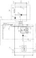
図1は、本発明に係る電源回路の第1の実施形態を示す概略ブロック図である。 FIG. 1 is a schematic block diagram showing a first embodiment of a power supply circuit according to the present invention.
第1の実施形態に係る電源回路は、図1に示すように、入力回路部10と、変圧器20と、を有している。
As illustrated in FIG. 1, the power supply circuit according to the first embodiment includes an
入力回路部10は、図示を省略した電源部から供給される入力電圧が、所定の電圧範囲内にあって、電源回路が正常な動作を行っている場合には、当該入力電圧を変圧器20に供給する。入力回路部10は、このとき同時に、当該入力電圧を供給することにより変圧器20を励磁及び磁気リセットする際のエネルギーを蓄積する。ここで、入力回路部10に蓄積されるエネルギーに基づく電圧は、上記入力電圧よりも高い電圧となるように設定されている。
When the input voltage supplied from the power supply unit (not shown) is within a predetermined voltage range and the power supply circuit is operating normally, the
また、入力回路部10は、入力電圧が所定の電圧範囲外にある場合には、電源部からの入力電圧に替えて、上記蓄積されたエネルギーに基づく電圧を、入力電圧として変圧器20に供給する。ここで、入力電圧が所定の電圧範囲外にある場合とは、具体的には、例えば電源部からの入力電圧の瞬時低下や瞬時遮断等の異常が発生した場合を意味する。
Further, when the input voltage is outside the predetermined voltage range, the
変圧器20は、上記入力電圧を、図示を省略した負荷の動作制御に必要とされる所望の出力電圧に変換する。
The
そして、このような構成を有する電源回路は、次のように動作する。 The power supply circuit having such a configuration operates as follows.
まず、入力回路部10において、電源部から供給される入力電圧を検出し、当該入力電圧が所定の電圧範囲内にあるか否かが監視される。入力電圧が所定の電圧範囲内にあると判定された場合には、入力回路部10は、当該入力電圧を変圧器20に供給するとともに、変圧器20を励磁及び磁気リセットするエネルギーに基づいて、入力電圧よりも高い電圧を充電する正常動作を行う。これにより、変圧器20は入力電圧に基づいて所定の出力電圧を生成して負荷に供給する。したがって、負荷は、供給された出力電圧に基づいて正常な動作を実行することができる。
First, the
一方、電源部から供給される入力電圧の瞬時低下や瞬時遮断等の異常が発生して、所定の電圧範囲外にあると判定された場合には、入力回路部10は、電源部からの入力電圧に替えて、上記正常動作時に充電された充電電圧に基づく電圧を、入力電圧として変圧器20に供給する。これにより、変圧器20は正常動作時に充電された充電電圧に基づく入力電圧に基づいて所定の出力電圧を生成して負荷に供給する。このとき、上記充電電圧は電源部から供給される入力電圧よりも高い電圧に設定されているので、負荷は長時間にわたって正常な動作を継続することができる。
On the other hand, when an abnormality such as instantaneous drop or instantaneous interruption of the input voltage supplied from the power supply unit occurs and it is determined that the input voltage is outside the predetermined voltage range, the
次に、上述した実施形態に係る電源回路を備えた電子機器について説明する。 Next, an electronic apparatus including the power supply circuit according to the above-described embodiment will be described.
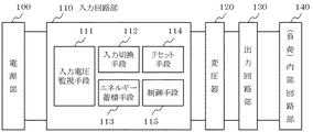
図2は、第1の実施形態に係る電源回路を備えた電子機器を示す概略ブロック図である。ここでは、図1に示した構成を含み、バッテリ等の電源部から供給される直流電圧からなる入力電圧を所定の出力電圧に変換し、負荷である内部回路部に供給する電源回路を備えた電子機器について説明する。また、本発明に係る電子機器としては、携帯型の通信端末や音響機器等を適用例とすることができる。 FIG. 2 is a schematic block diagram illustrating an electronic device including the power supply circuit according to the first embodiment. 1 includes a power supply circuit including the configuration shown in FIG. 1 and converting an input voltage composed of a DC voltage supplied from a power supply unit such as a battery into a predetermined output voltage and supplying the output voltage to an internal circuit unit as a load. The electronic device will be described. In addition, as an electronic device according to the present invention, a portable communication terminal, an audio device, or the like can be used as an application example.
上述した第1の実施形態に係る電源回路を備えた電子機器は、図2に示すように、電源部100と、入力回路部110と、変圧器120と、出力回路部130と、負荷140と、を有している。
As shown in FIG. 2, the electronic device including the power supply circuit according to the first embodiment described above includes a
電源部100は、所定の入力電圧を入力回路部110に供給する。電源部100は、例えばバッテリ等の直流電圧源であってもよいし、商用電源等からの交流電圧を整流処理することにより直流電圧に変換し、入力電圧として出力するものであってもよい。
The
入力回路部110は、図1に示した入力回路部10に対応し、変圧器120は、図1に示した変圧器20に対応する。入力回路部110、変圧器120及び出力回路部130は、上記入力電圧を負荷140の動作制御に必要とされる所望の出力電圧に変換する。ここで、負荷140は、具体的には、出力電圧に基づいて、例えば通信制御や映像表示動作等の各種の動作機能を実現する電子機器の内部回路部である。
The input circuit unit 110 corresponds to the
入力回路部110は、より具体的には、例えば図2に示すように、入力電圧監視手段111と、入力切換手段112と、エネルギー蓄積手段113と、リセット手段114と、制御手段115と、を備えた構成を適用することができる。
More specifically, the input circuit unit 110 includes an input voltage monitoring unit 111, an
入力電圧監視手段111は、電源部100から入力回路部110に供給される入力電圧(直流電圧)を検出し、所定の電圧範囲内にあるか否かを判定し、その判定に応じて、入力切換手段112を切り換え制御する制御信号を出力する。入力切換手段112は、入力電圧監視手段111からの制御信号に基づいて、変圧器120の入力側と、電源部100又はエネルギー蓄積手段113との接続経路を選択的に切り換える。エネルギー蓄積手段113は、励磁された変圧器120を磁気リセットする際の電圧と、この磁気リセット動作の際に放出される変圧器120の励磁エネルギーを蓄積する。リセット手段114は、所定のリミット制御された電圧で変圧器120を磁気リセットする。制御手段115は、例えばスイッチング素子を有し、変圧器120への入力電圧の供給、遮断を所定のタイミングで切り換え制御することにより、出力回路部130から負荷140に供給される出力電圧を安定化するための制御を行う。
The input voltage monitoring unit 111 detects an input voltage (DC voltage) supplied from the
そして、このような構成を有する電子機器(特に、電源回路)は、次のように動作する。 And the electronic device (especially power supply circuit) which has such a structure operate | moves as follows.
上述した構成を有する電子機器(電源回路)において、まず、電源部100から入力回路部10に供給される入力電圧が、入力電圧監視手段111により検出される。入力電圧監視手段111は、検出された入力電圧が所定の電圧範囲内にあると判定した場合には、入力切換手段112を制御して変圧器120の入力源を電源部100側に設定する。これにより、所定の入力電圧が、電源部100から入力切換手段112を介して変圧器120に供給される。
In the electronic device (power supply circuit) having the above-described configuration, first, the input voltage supplied from the
この状態において、制御手段115は、変圧器120の一次側への上記入力電圧の供給状態を制御して所定のタイミングで入力電圧の供給、遮断を繰り返す。ここで、変圧器120に入力電圧が供給されるタイミングにおいては、変圧器120に励磁エネルギーが蓄積される。一方、変圧器120への入力電圧が遮断されるタイミングにおいては、変圧器120に蓄積された励磁エネルギーがエネルギー蓄積手段113に放出されるとともに、変圧器120の二次側から所定の出力電圧が出力回路部130へ出力される。
In this state, the control means 115 controls the supply state of the input voltage to the primary side of the
これにより、変圧器120は入力電圧に基づいて所定の出力電圧を生成する。該出力電圧は、出力回路部130を介して電子機器の内部回路部である負荷140に供給される。また、このとき、変圧器120を磁気リセットする際の電圧と、このリセット動作により変圧器120から放出される励磁エネルギーがエネルギー蓄積手段113に蓄積される。
Thereby, the
そして、入力電圧監視手段111は、電源部100から供給される入力電圧の瞬時低下や瞬時遮断等の異常を検出した場合には、入力切換手段112を制御して変圧器120の入力源を電源部100側からエネルギー蓄積手段113側に切り換える。これにより、エネルギー蓄積手段113から、上記の動作により蓄積されたエネルギーに応じた所定の入力電圧が、変圧器120の一次側に供給される。変圧器120の二次側から出力される出力電圧は、出力回路部130を介して負荷140に供給される。
When the input voltage monitoring unit 111 detects an abnormality such as an instantaneous drop or instantaneous interruption of the input voltage supplied from the
したがって、上述した実施形態に係る電源回路を備えた電子機器においては、電源部100からの入力電圧に瞬時低下や瞬時遮断等の異常が発生した場合であっても、負荷140である内部回路部に対して、安定的に出力電圧を供給する動作を継続することができる。これにより、電子機器は、
所定の出力電圧に基づいて、通信制御や映像表示動作等の各種の動作を継続して実行することができる。
Therefore, in the electronic device including the power supply circuit according to the above-described embodiment, even when an abnormality such as a momentary drop or a momentary interruption occurs in the input voltage from the
Based on the predetermined output voltage, various operations such as communication control and video display operation can be continuously executed.
また、上述した電源回路を備えた電子機器においては、電源部100から供給される入力電圧が所定の電圧範囲内にある場合(正常動作時)に、エネルギー蓄積手段113に蓄積される電圧が、電源部100からの入力電圧よりも高く設定される。これは、次のような理由による。変圧器120を磁気リセットする際の電圧は、制御手段115により変圧器120への入力電圧を遮断している期間の制御手段115に設けられるスイッチング素子のキャパシタンスや、リセット手段114の回路特性に依存する。本願発明者は、この磁気リセット時の電圧が電源部100から供給される入力電圧よりも高いピーク電圧を有し、その電圧値が入力電圧の2〜3倍になることを確認した。
Moreover, in the electronic device provided with the above-described power supply circuit, when the input voltage supplied from the
そこで、本願発明者は、この点に着目して、電源回路を次のように構成した。すなわち、入力回路部110は、電源部100から供給される入力電圧(直流電圧)が所定の電圧範囲内にある場合に、変圧器120の磁気リセット時の電圧と、当該磁気リセット時に変圧器120から放出される励磁エネルギーを、エネルギー蓄積手段113に蓄積するように構成されている。これにより、エネルギー蓄積手段113には、入力電圧よりも十分高い電圧が充電される。
Therefore, the inventor of the present application paid attention to this point and configured the power supply circuit as follows. That is, when the input voltage (DC voltage) supplied from the
したがって、電源部100から供給される入力電圧の瞬時低下や瞬時遮断等の異常が発生した時に、エネルギー蓄積手段113から変圧器120へ電圧を供給することにより、変圧器120が正常に動作可能な電圧範囲の下限よりも十分高い電圧を供給することができる。それ故、本実施形態によれば、電源回路内に昇圧コンバータやその制御回路等を設けることなく、出力電圧の安定的な供給動作を維持できる時間を長くすることができ、電子機器を安定的に動作させることができる。
Therefore, when an abnormality such as an instantaneous drop or instantaneous interruption of the input voltage supplied from the
<第2の実施形態>
次に、本発明に係る電源回路の第2の実施形態について、図面を参照して詳細に説明する。
<Second Embodiment>
Next, a second embodiment of the power supply circuit according to the present invention will be described in detail with reference to the drawings.
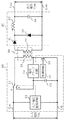
図3は、本発明に係る電子機器に適用可能な電源回路の第2の実施形態を示す概略回路図である。ここでは、図3に、電源部を省略した電源回路(入力回路部、変圧器及び出力回路部のみ)を示す。また、本実施形態においては、電源回路として、フォワード型スイッチング電源回路を示して説明する。 FIG. 3 is a schematic circuit diagram showing a second embodiment of the power supply circuit applicable to the electronic apparatus according to the present invention. Here, FIG. 3 shows a power supply circuit (only the input circuit unit, the transformer, and the output circuit unit) in which the power supply unit is omitted. In the present embodiment, a forward switching power supply circuit is shown and described as the power supply circuit.
第2の実施形態に係る電源回路は、図3に示すように、変圧器20と、変圧器20の前段(入力側)に設けられる入力回路部10と、変圧器20の後段(出力側)に設けられる出力回路部30と、を有している。
As shown in FIG. 3, the power supply circuit according to the second embodiment includes a
本実施形態に適用される入力回路部10は、少なくとも、入力電圧監視回路11と、切換スイッチ12と、コンデンサ13と、電圧クランプ回路14と、制御回路15と、スイッチング素子16と、を備えている。ここで、本実施形態における入力電圧監視回路11は、本発明に係る入力電圧監視手段に相当し、本実施形態における切換スイッチ12は、本発明に係る入力切換手段に相当する。また、本実施形態におけるコンデンサ13は、本発明に係るエネルギー蓄積手段に相当し、本実施形態における電圧クランプ回路14は、本発明に係るリセット手段に相当する。また、本実施形態における制御回路15及びスイッチング素子16は、本発明に係る制御手段に相当する。
The
入力電圧監視回路11は、図示を省略した電源部から入力回路部10に供給される入力電圧(直流電圧)Vinを検出し、その検出結果に基づいて切換スイッチ12を切り換え設定する。入力電圧監視回路11は、具体的には、電源入力線(給電線)LiaとLibとの間に設けられる。そして、入力電圧監視回路11は、検出された入力電圧Vinが、所定の正常入力電圧範囲内にあるか否かの判定に応じて、切換スイッチ12を切り換え設定するための制御信号を出力する。
The input
切換スイッチ12は、入力電圧監視回路11から出力される制御信号に基づいて、変圧器20の一次巻線21の一端側と、電源入力線Lia側のa接点又はコンデンサ13側のb接点のいずれかと、を選択的に接続するように切り換える。ここで、切換スイッチ12は、図中ではスイッチ記号を使用して表記したが、本発明はこれに限定されるものではなく、接続経路の切り換えが実現できるものであれば、他の種類の素子や回路を用いるものであってもよい。
Based on the control signal output from the input
コンデンサ13は、切換スイッチ12のb接点と電源入力線Libとの間に設けられる。コンデンサ13は、切換スイッチ12の接続状態に応じて、変圧器20の一次巻線21側から電圧クランプ回路14を介して供給される電力を蓄積する動作と、蓄積した電力に基づく電圧を、入力電圧として変圧器20の一次巻線21側に供給する動作を実行する。特に、本実施形態においては、コンデンサ13は、上記の電圧蓄積動作において、変圧器20の磁性体に励磁されるエネルギーと、該磁性体を磁気リセットするための電圧を蓄積する。
The
電圧クランプ回路14は、切換スイッチ12のb接点と変圧器20の一次巻線21の他端側(一次巻線21とスイッチング素子16の接続接点)との間に設けられる。すなわち、電圧クランプ回路14は、入力電圧監視回路11により検出された入力電圧Vinが、所定の電圧範囲内にある場合には、所定のリミット制御された電圧で変圧器20の磁性体を磁気リセットする。ここで、磁気リセット時の電圧が、電圧クランプ回路14のクランプ電圧を超過している間は、コンデンサ13に充電動作が行われる。
The
スイッチング素子16は、変圧器20の一次巻線21の他端側に直列に接続されている。スイッチング素子16は、具体的には、例えば電界効果型のトランジスタが適用され、電流路の一端側が一次巻線21に接続されるとともに、同他端側が電源入力線Libに接続されている。また、スイッチング素子16の制御端子は、制御回路15に接続されている。
The switching
制御回路15は、電源回路の出力電圧Voutが安定するように、スイッチング素子16の導通状態を制御するための制御信号を生成して出力する。制御回路15は、具体的には、スイッチング素子16を所定のタイミングでオン、オフ制御することにより、変圧器20の一次巻線21と電源入力線Libとを周期的に接続、切り離した状態に設定する。これにより、変圧器20の一次巻線21への入力電圧の供給状態(供給、遮断)が制御される。
The
変圧器20は、一次巻線21及び二次巻線22を有するトランスである。一次巻線21は、入力回路部10側のスイッチング素子16と直列に接続され、この直列回路が、電源入力線LiaとLibの間に接続されている。二次巻線22は、出力回路部30を介して、出力線LoaとLobの間に接続されている。
The
出力回路部30は、チョークインプット型の平滑回路であって、少なくとも、ダイオード31、32と、チョークコイル33と、出力コンデンサ34と、を備えている。ダイオード31とチョークコイル33は、変圧器20の二次巻線22の一端側と出力線Loaとの間に、直列に接続されている。ダイオード32は、ダイオード31とチョークコイル33の接続接点と出力線Lobとの間に接続されている。また、出力コンデンサ34は、出力線LoaとLobとの間に接続されている。このような出力回路部30は、変圧器20の二次巻線22側に生成される電圧成分を平滑化した直流電圧を、図示を省略した電子機器の内部回路部(負荷)に出力電圧Voutとして供給する。
The
次いで、本実施形態に係る電源回路の動作(制御方法)について説明する。 Next, the operation (control method) of the power supply circuit according to the present embodiment will be described.
電源部から上述した電源回路へ供給される入力電圧(直流電圧)Vinは、入力電圧監視回路11により検出される。ここで、検出された入力電圧Vinが所定の正常入力電圧範囲内にあれば、入力電圧監視回路11は、入力電圧Vinが変圧器20へ供給されるように、切換スイッチ12を制御する。すなわち、入力電圧監視回路11は、変圧器20の一次巻線21が電源入力線Liaに接続されるように、切換スイッチ12をa接点側に切り換えるための制御信号を生成して出力する。
An input voltage (DC voltage) Vin supplied from the power supply unit to the above-described power supply circuit is detected by the input
入力電圧Vinが所定の正常入力電圧範囲内にあって、制御回路15によりスイッチング素子16がオン動作している状態では、入力電圧Vinが変圧器20の一次巻線21に供給されることにより、変圧器20の磁性体に励磁エネルギーが蓄積される。一方、制御回路15によりスイッチング素子16がオフ動作している状態では、変圧器20への入力電圧Vinが遮断されることにより、変圧器20に蓄積された励磁エネルギーに基づいて二次巻線22に所定の出力電圧が生成されて出力回路部30へ出力される。また、変圧器20に蓄積された励磁エネルギーは電圧クランプ回路14を介してコンデンサ13に放出される。このとき、電圧クランプ回路14によってリミット制御された電圧により、変圧器20の磁性体が磁気リセットされる。この磁気リセット時の電圧は、電圧クランプ回路14のクランプ電圧を超えている間、コンデンサ13に充電される。
When the input voltage Vin is within a predetermined normal input voltage range and the switching
ここで、コンデンサ13の充電状態は、電源起動直後においてはコンデンサ13に充電されている電荷は少ないが、制御回路15によりスイッチング素子16を周期的にオン、オフ制御することにより、このスイッチング動作の度にコンデンサ13が充電される。この充電動作は、コンデンサ13の充電電圧が、上記電圧クランプ回路14のクランプ電圧に達するまで継続される。本実施形態においては、コンデンサ13の充電電圧が入力電圧Vinよりも高くなるように、電圧クランプ回路14のクランプ電圧を設定する。
Here, the charge state of the
入力電圧Vinが電源回路の正常動作を維持できない電圧まで低下した場合、入力電圧監視回路11は入力電圧Vinの異常低下を検出すると、切換スイッチ12に制御信号を出力してb接点側に切り換え設定する。これにより、変圧器20にはコンデンサ13から給電が行われる。ここで、コンデンサ13から変圧器20に供給される電圧は、上述した充電動作によりコンデンサ13に充電された電圧に依存する値となる。
When the input voltage Vin drops to a voltage at which the normal operation of the power supply circuit cannot be maintained, when the input
電源部から供給される入力電圧Vinが正常入力電圧範囲内に復帰した場合、入力電圧監視回路11は入力電圧Vinの正常範囲復帰を検出すると、切換スイッチ12に制御信号を出力してa接点側に切り換え設定する。これにより、変圧器20には図示を省略した電源部から給電が行われ、当初の動作と同様に、電源回路が正常動作するとともに、コンデンサ13への充電動作が再び開始される。
When the input voltage Vin supplied from the power supply unit returns to the normal input voltage range, the input
ところで、電子機器に適用される電源回路においては、変圧器20及び出力回路部30を介して、図示を省略した内部回路部(負荷)に供給される出力電圧Voutが、電子機器の駆動電圧の範囲内に設定されるように制御する必要がある。そのため、本実施形態に係る電源回路においては、例えば電子機器の内部回路部等から出力される制御信号等に基づいて、入力回路部10に設けられた制御回路15がスイッチング素子16の導通状態を制御することにより、出力電圧を安定化させる。
By the way, in the power supply circuit applied to the electronic device, the output voltage Vout supplied to the internal circuit unit (load) (not shown) via the
これにより、本実施形態に係る電源回路においては、入力電圧Vinの瞬時低下や瞬時遮断等の異常発生時には、コンデンサ13に充電された電圧に基づいて、入力電圧として変圧器20に供給することができる。したがって、本実施形態に係る電源回路によれば、出力電圧Voutの安定的な供給動作を持続させることができる。
Thereby, in the power supply circuit according to the present embodiment, when an abnormality such as an instantaneous decrease in the input voltage Vin or an instantaneous interruption occurs, the input voltage is supplied to the
また、この場合、電源回路が動作可能な電圧範囲の下限よりも十分高い電圧が、コンデンサ13から変圧器20に入力電圧として供給される。したがって、本実施形態に係る電源回路によれば、電源回路内に昇圧コンバータやその制御回路等を設けることなく、比較的簡易な回路構成で、出力電圧の安定的な供給動作を維持できる時間を長くすることができる。
In this case, a voltage sufficiently higher than the lower limit of the voltage range in which the power supply circuit can operate is supplied from the
なお、本実施形態においては、出力回路部として、チョークインプット型の平滑回路を適用した構成を示したが、本発明はこれに限定されるものではない。本発明に係る電源回路に適用される出力回路部は、変圧器20により生成された電圧を、電子機器の駆動電圧に対応した出力電圧Voutに調整することができるものであれば他の回路構成を有するものであってもよい。
In the present embodiment, a configuration in which a choke input type smoothing circuit is applied as the output circuit unit is shown, but the present invention is not limited to this. The output circuit unit applied to the power supply circuit according to the present invention may have other circuit configurations as long as the voltage generated by the
<第3の実施形態>
次に、本発明に係る電源回路の第3の実施形態について、図面を参照して詳細に説明する。
<Third Embodiment>
Next, a third embodiment of the power supply circuit according to the present invention will be described in detail with reference to the drawings.
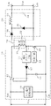
図4は、本発明に係る電子機器に適用可能な電源回路の第3の実施形態の一構成例を示す概略回路図である。図5は、本発明に係る電子機器に適用可能な電源回路の第3の実施形態の他の構成例を示す概略回路図である。ここで、上述した第2の実施形態と同等の構成については、その説明を簡略化又は省略する。 FIG. 4 is a schematic circuit diagram showing a configuration example of the third embodiment of the power supply circuit applicable to the electronic apparatus according to the present invention. FIG. 5 is a schematic circuit diagram showing another configuration example of the third embodiment of the power supply circuit applicable to the electronic apparatus according to the invention. Here, the description of the configuration equivalent to that of the above-described second embodiment is simplified or omitted.
第3の実施形態に係る電源回路の一構成例は、図4に示すように、上述した第2の実施形態に示した電源回路において、電圧クランプ回路14と切換スイッチ12のb接点との間に、整流素子17を追加した回路構成を有している。また、コンデンサ13は、上述した第2の実施形態と同様に、切換スイッチ12のb接点と電源入力線Libとの間に接続される。ここで、本実施形態における整流素子17は、本発明に係る整流手段に相当する。
One configuration example of the power supply circuit according to the third embodiment is as shown in FIG. 4, in the power supply circuit shown in the second embodiment described above, between the
そして、このような構成を有する電源回路は、次のように動作する。 The power supply circuit having such a configuration operates as follows.
上述したような回路構成において、電源回路が正常動作を行っている間は、第2の実施形態に示した電源回路の動作と同様に、電圧クランプ回路14によってリミット制御された電圧で、変圧器20の磁性体が磁気リセットされる。このとき、磁気リセット時の電圧が、電圧クランプ回路14のクランプ電圧を超えている間は、コンデンサ13が充電される。
In the circuit configuration as described above, during the normal operation of the power supply circuit, the voltage is controlled by the
ここで、本実施形態においては、電圧クランプ回路14の出力側に整流素子17が設けられていることにより、電圧クランプ回路14における電流の逆流が防止される。そのため、コンデンサ13に充電されるピーク電圧は、上述した第2の実施形態の場合に比較して高くなる。これにより、入力電圧Vinの異常低下等が発生した場合には、コンデンサ13に充電された高電圧に基づく入力電圧が変圧器20に供給される。したがって、本実施形態に係る電源回路によれば、出力電圧Voutの安定的な供給動作を維持できる時間をさらに長くすることができる。
Here, in the present embodiment, since the rectifying
なお、図4においては、第2の実施形態に示した電源回路において、整流素子17のみを追加した回路構成を示したが、本発明はこれに限定されるものではない。本発明に係る電源回路は、例えば図5に示すように、整流素子17及び補助コンバータ回路18を追加した回路構成を有するものであってもよい。
4 shows a circuit configuration in which only the rectifying
第3の実施形態に係る電源回路の他の構成例は、図5に示すように、上述した第2の実施形態に示した電源回路において、電圧クランプ回路14と切換スイッチ12のb接点との間に、整流素子17と、補助コンバータ回路18とを追加した回路構成を有している。また、コンデンサ13は、整流素子17と補助コンバータ回路18の接続接点と、電源入力線Libとの間に接続される。ここで、本実施形態における補助コンバータ回路18は、本発明に係る電圧調整手段に相当する。
As shown in FIG. 5, another configuration example of the power supply circuit according to the third embodiment includes a
本構成例においても、図4に示した回路構成と同様に、電圧クランプ回路14の出力側に整流素子17が設けられていることにより、コンデンサ13に充電されるピーク電圧が高くなる。そのため、コンデンサ13の充放電動作に伴う電圧変化が大きくなる。本構成例においては、コンデンサ13と変圧器20の一次巻線21との間に、補助コンバータ回路18が介在することにより、コンデンサ13の充放電動作に伴う電圧変化を緩和(安定化)させることができる。これにより、電源回路(入力回路部10)を上記電圧変化に耐えられるように設計することができない場合であっても、コンデンサ13の充電電圧に基づいて、変圧器20の一次巻線21に供給される入力電圧の電圧値を制御することができる。したがって、本実施形態によれば、コンデンサ13の電圧変化に対応させて電源回路の耐圧を高める必要がないので、回路設計の自由度を確保しつつ、製品コストの上昇を抑制することができる。
Also in this configuration example, as in the circuit configuration illustrated in FIG. 4, the rectifying
なお、本実施形態に適用される補助コンバータ回路18は、電源回路の既定の耐圧に基づいて、コンデンサ13に充電された電圧を調整して変圧器20に供給すればよいので、電圧変換機能として高い精度は要求されない。
The
<第4の実施形態>
次に、本発明に係る電源回路の第4の実施形態について、図面を参照して詳細に説明する。
<Fourth Embodiment>
Next, a fourth embodiment of the power supply circuit according to the present invention will be described in detail with reference to the drawings.
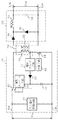
図6は、本発明に係る電子機器に適用可能な電源回路の第4の実施形態を示す概略回路図である。ここで、上述した第2又は第3の実施形態と同等の構成については、その説明を簡略化又は省略する。 FIG. 6 is a schematic circuit diagram showing a fourth embodiment of a power supply circuit applicable to the electronic apparatus according to the present invention. Here, the description of the configuration equivalent to the second or third embodiment described above is simplified or omitted.
第4の実施形態に係る電源回路は、上述した各実施形態と同様に、図6に示すように、入力回路部10と、変圧器20と、出力回路部30と、を有している。
The power supply circuit according to the fourth embodiment includes an
本実施形態に適用される入力回路部10は、少なくとも、入力電圧監視回路11と、コンデンサ13と、電圧クランプ回路14と、制御回路15と、スイッチング素子16a、16bと、整流素子17と、を備えている。ここで、本実施形態における制御回路15及びスイッチング素子16a、16bは、本発明に係る入力切換手段及び制御手段に相当する。
The
入力電圧監視回路11は、上述した第2の実施形態と同様に、電源入力線Lia、Lib間に設けられる。ここで、入力電圧監視回路11は、入力電圧(直流電圧)Vinが所定の正常入力電圧範囲内にあるか否かに応じてスイッチング素子16a、16bを所定の導通状態で動作させるための制御信号を制御回路15に出力する。
The input
コンデンサ13は、接点Ncと電源入力線Libとの間に設けられる。
The
電圧クランプ回路14及び整流素子17は、接点Ncと変圧器20の一次巻線21aの他端側(一次巻線21aとスイッチング素子16aの接続接点)との間に、直列に接続される。
The
スイッチング素子16aは、電流路の一端側が一次巻線21aに接続されるとともに、同他端側が電源入力線Libに接続されている。スイッチング素子16bは、電流路の一端側が一次巻線21bに接続されるとともに、同他端側が電源入力線Libに接続されている。また、スイッチング素子16a、16bの制御端子は、制御回路15に接続されている。
The switching
制御回路15は、入力電圧監視回路11からの制御信号に基づいて、スイッチング素子16a、16bの一方をオン、他方をオフ制御することにより、変圧器20の一次巻線21a側又は21b側のいずれか一方を駆動状態に設定する。そして、駆動状態に設定された一次巻線への入力電圧の供給により、所定の出力電圧Voutが生成されるように、制御回路15は、当該駆動状態に設定された一次巻線側のスイッチング素子16a、16bを周期的にオン、オフ制御する。
Based on the control signal from the input
変圧器20は、一次側の巻線として、電源入力線Liaに直接接続された一次巻線21aに加え、コンデンサ13に接続された一次巻線21bを設けた構成を有している。変圧器20の一次巻線21aとスイッチング素子16aは、電源入力線LiaとLibとの間に、直列に接続されている。また、変圧器20の一次巻線21bとスイッチング素子16bは、上記接点Ncと電源入力線Libとの間に、直列に接続されている。ここで、一次巻線21bは、電源回路の正常動作時にコンデンサ13に充電されるピーク電圧及び電圧変化に十分耐えられるように耐圧が設定されている。
The
なお、出力回路部30については、上述した第2の実施形態と同等であるので、その説明を省略する。
Since the
このような回路構成を有する電源回路において、電源回路の正常動作時には、制御回路15は、入力電圧監視回路11からの制御信号に基づいて、スイッチング素子16aをオン動作させるとともに、スイッチング素子16bをオフ動作させるように制御する。これにより、入力電圧Vinが変圧器20の一次巻線21aに供給される。すなわち、入力電圧Vinが所定の正常入力電圧範囲内にある場合には、制御回路15によりスイッチング素子16aを周期的にオン、オフ制御することにより、変圧器20の二次巻線22に所定の出力電圧が生成されるとともに、コンデンサ13が充電される。ここで、電圧クランプ回路14の出力に整流素子17が設けられていることにより、コンデンサ13に充電されるピーク電圧は、上述した第2の実施形態の場合に比較して高くなる。
In the power supply circuit having such a circuit configuration, during normal operation of the power supply circuit, the
そして、入力電圧の異常低下等が発生した場合には、制御回路15は、入力電圧監視回路11からの制御信号に基づいて、スイッチング素子16aをオフ動作させるとともに、スイッチング素子16bをオン動作させるように制御する。これにより、コンデンサ13の充電電圧に基づく入力電圧が変圧器20の一次巻線21bに供給される。この状態において、制御回路15によりスイッチング素子16bを周期的にオン、オフ制御することにより、変圧器20の二次巻線22に所定の出力電圧が生成される。
When an abnormal decrease in the input voltage occurs, the
したがって、本実施形態によれば、入力電圧の異常低下等が発生した場合であっても、出力電圧Voutの安定的な供給動作を持続させることができる。また、この場合、電源回路が動作可能な電圧範囲の下限よりも十分高い電圧が、コンデンサ13から変圧器20に供給されるので、本実施形態によれば、出力電圧Voutの安定的な供給動作を維持できる時間を長くすることができる。さらに、本実施形態によれば、コンデンサ13の電圧変化が大きい場合であっても、当該電圧変化に対応するように、一次巻線21bの耐圧が設定されているので、電源回路を正常に動作させることができる。
Therefore, according to the present embodiment, a stable supply operation of the output voltage Vout can be maintained even when an abnormal decrease in the input voltage occurs. In this case, since a voltage sufficiently higher than the lower limit of the voltage range in which the power supply circuit can operate is supplied from the
本発明の電源回路及びその制御方法は、変圧器の磁性体に蓄積された励磁エネルギーを、自己リセット(共振リセット)する回路構成を有する電源回路を備えた電子機器に良好に適用することができる。これにより、電源電圧の瞬時低下や瞬時遮断等が発生した場合であっても、負荷である電子機器の内部回路部に出力電圧を安定的に供給する動作を長時間にわたり維持することができるので、電子機器の所定の動作機能を正常に実行することができる。 INDUSTRIAL APPLICABILITY The power supply circuit and the control method thereof according to the present invention can be favorably applied to an electronic device having a power supply circuit having a circuit configuration that self-resets (resonance reset) the excitation energy accumulated in the magnetic body of the transformer. . As a result, even when an instantaneous drop in the power supply voltage or an instantaneous interruption occurs, the operation of stably supplying the output voltage to the internal circuit part of the electronic device as the load can be maintained for a long time. The predetermined operation function of the electronic device can be normally executed.
10 入力回路部
11 入力電圧監視回路
12 切換スイッチ
13 コンデンサ
14 電圧クランプ回路
15 制御回路
16、16a、16b スイッチング素子
17 整流素子
18 補助コンバータ回路
20 変圧器
21、21a、21b 一次巻線
22 二次巻線
30 出力回路部
100 電源部
110 入力回路部
111 入力電圧監視手段
112 入力切換手段
113 エネルギー蓄積手段
114 リセット手段
115 制御手段
120 変圧器
130 出力回路部
140 負荷(内部回路部)
DESCRIPTION OF
Claims (12)
前記入力電圧が所定の電圧範囲内にある場合には、前記入力電圧を前記変圧器に供給するとともに、前記変圧器を励磁及び磁気リセットするエネルギーに基づいて、前記入力電圧よりも高い電圧を充電し、前記入力電圧が前記電圧範囲外にある場合には、前記充電された充電電圧に基づく電圧を、前記入力電圧として前記変圧器に供給する入力回路部と、
を有していることを特徴とする電源回路。 A transformer that converts input voltage to output voltage;
When the input voltage is within a predetermined voltage range, the input voltage is supplied to the transformer, and a voltage higher than the input voltage is charged based on energy for exciting and magnetically resetting the transformer. When the input voltage is outside the voltage range, an input circuit unit that supplies a voltage based on the charged charge voltage to the transformer as the input voltage;
A power supply circuit comprising:
電源部から供給される前記入力電圧を検出する入力電圧監視手段と、
前記入力電圧監視手段により前記入力電圧が所定の電圧範囲内にあると判定された場合には、励磁された前記変圧器を磁気リセットする際の電圧と、当該磁気リセットの際に前記変圧器から放出される励磁エネルギーに基づいて、前記入力電圧よりも高い電圧を充電し、前記入力電圧監視手段により前記入力電圧が前記所定の電圧範囲外にあると判定された場合には、前記充電電圧に基づく電圧を、前記入力電圧として前記変圧器に供給するエネルギー蓄積手段と、
前記入力電圧監視手段による検出結果に基づいて、前記変圧器への前記入力電圧の供給経路を、前記電源部側又は前記エネルギー蓄積手段側のいずれか一方に切り換える入力切換手段と、
を含むことを特徴とする請求項1記載の電源回路。 The input circuit unit is
Input voltage monitoring means for detecting the input voltage supplied from a power supply unit;
When the input voltage monitoring means determines that the input voltage is within a predetermined voltage range, the voltage at the time of magnetic resetting the excited transformer, and the transformer at the time of the magnetic reset A voltage higher than the input voltage is charged based on the released excitation energy, and when the input voltage monitoring means determines that the input voltage is outside the predetermined voltage range, the charge voltage is Energy storage means for supplying a voltage based on the input voltage to the transformer;
Based on the detection result by the input voltage monitoring means, the input voltage switching means for switching the supply path of the input voltage to the transformer to either the power supply unit side or the energy storage means side;
The power supply circuit according to claim 1, comprising:
前記入力電圧を前記変圧器に供給するとともに、前記変圧器を励磁及び磁気リセットするエネルギーに基づいて、前記入力電圧よりも高い電圧を充電するステップと、
前記入力電圧が所定の電圧範囲外にあると判定された場合に、前記充電された充電電圧に基づく電圧を、前記入力電圧として前記変圧器に供給するステップと、
を含むことを特徴とする電源回路の制御方法。 Detecting an input voltage supplied to the transformer and monitoring whether the input voltage is within a predetermined voltage range;
Charging the input voltage to the transformer and charging a voltage higher than the input voltage based on energy to excite and magnetically reset the transformer;
Supplying the voltage based on the charged charging voltage to the transformer as the input voltage when it is determined that the input voltage is outside a predetermined voltage range;
A method for controlling a power supply circuit, comprising:
請求項1乃至8のいずれかに記載の前記電源回路を有し、前記入力電圧に基づいて所定の出力電圧を生成する電力変換部と、
前記電力変換部から供給される前記出力電圧に基づいて所定の動作機能を実行する内部回路部と、
を備えることを特徴とする電子機器。 A power supply for supplying a predetermined input voltage;
A power converter having the power supply circuit according to claim 1 and generating a predetermined output voltage based on the input voltage;
An internal circuit unit that performs a predetermined operation function based on the output voltage supplied from the power conversion unit;
An electronic device comprising:
Priority Applications (1)
| Application Number | Priority Date | Filing Date | Title |
|---|---|---|---|
| JP2008225165A JP2010063243A (en) | 2008-09-02 | 2008-09-02 | Power supply circuit, its control method and electronic equipment |
Applications Claiming Priority (1)
| Application Number | Priority Date | Filing Date | Title |
|---|---|---|---|
| JP2008225165A JP2010063243A (en) | 2008-09-02 | 2008-09-02 | Power supply circuit, its control method and electronic equipment |
Publications (1)
| Publication Number | Publication Date |
|---|---|
| JP2010063243A true JP2010063243A (en) | 2010-03-18 |
Family
ID=42189434
Family Applications (1)
| Application Number | Title | Priority Date | Filing Date |
|---|---|---|---|
| JP2008225165A Pending JP2010063243A (en) | 2008-09-02 | 2008-09-02 | Power supply circuit, its control method and electronic equipment |
Country Status (1)
| Country | Link |
|---|---|
| JP (1) | JP2010063243A (en) |
Cited By (1)
| Publication number | Priority date | Publication date | Assignee | Title |
|---|---|---|---|---|
| JP2015109785A (en) * | 2013-09-04 | 2015-06-11 | 日東電工株式会社 | Mobile devices, charging systems, power circuit boards, etc. |
Citations (3)
| Publication number | Priority date | Publication date | Assignee | Title |
|---|---|---|---|---|
| JPH02133066A (en) * | 1988-11-09 | 1990-05-22 | Mitsubishi Electric Corp | Switching power supply |
| JPH11299275A (en) * | 1998-04-14 | 1999-10-29 | Osaka Gas Co Ltd | Power unit for elevator |
| JP2007053853A (en) * | 2005-08-18 | 2007-03-01 | Fuji Electric Holdings Co Ltd | Instantaneous low backup device |
-
2008
- 2008-09-02 JP JP2008225165A patent/JP2010063243A/en active Pending
Patent Citations (3)
| Publication number | Priority date | Publication date | Assignee | Title |
|---|---|---|---|---|
| JPH02133066A (en) * | 1988-11-09 | 1990-05-22 | Mitsubishi Electric Corp | Switching power supply |
| JPH11299275A (en) * | 1998-04-14 | 1999-10-29 | Osaka Gas Co Ltd | Power unit for elevator |
| JP2007053853A (en) * | 2005-08-18 | 2007-03-01 | Fuji Electric Holdings Co Ltd | Instantaneous low backup device |
Cited By (4)
| Publication number | Priority date | Publication date | Assignee | Title |
|---|---|---|---|---|
| JP2015109785A (en) * | 2013-09-04 | 2015-06-11 | 日東電工株式会社 | Mobile devices, charging systems, power circuit boards, etc. |
| US10218223B2 (en) | 2013-09-04 | 2019-02-26 | Nitto Denko Corporation | Portable device, charging system, and power source circuit substrate |
| US11056920B2 (en) | 2013-09-04 | 2021-07-06 | Nitto Denko Corporation | Portable device, charging system, and power source circuit substrate |
| US12191689B2 (en) | 2013-09-04 | 2025-01-07 | K/S Himpp | Portable device, charging system, and power source circuit substrate |
Similar Documents
| Publication | Publication Date | Title |
|---|---|---|
| US8829864B2 (en) | Current driver circuit | |
| JPWO2011036767A1 (en) | Uninterruptible power system | |
| US8368375B2 (en) | Switching regulator with transient control function and control circuit and method therefor | |
| JP2012120267A (en) | Charge controller | |
| JP6288773B2 (en) | Power converter | |
| JP3699082B2 (en) | Switching power supply circuit | |
| US20110255314A1 (en) | Switched power converter with extended hold-up time | |
| JP4049333B1 (en) | Charge control device | |
| JP2016010193A (en) | Power supply circuit for railway vehicle | |
| CN100403642C (en) | power conversion device | |
| JP2008099512A (en) | Power supply | |
| US8817490B2 (en) | DC-DC converter | |
| US7948306B2 (en) | Active power filter method and apparatus | |
| JP2007109609A (en) | Charge / discharge device for fuel cell system | |
| JP2011120416A (en) | Switching power supply device | |
| JP2009247187A (en) | Power converter and its control method | |
| JP2010063243A (en) | Power supply circuit, its control method and electronic equipment | |
| JP2008289266A (en) | DC / DC power converter | |
| JP5660575B2 (en) | Control circuit and switching power supply | |
| JP5954256B2 (en) | Control method | |
| JP2006158137A (en) | Switching power supply | |
| JP6692168B2 (en) | Power storage device having UPS function and method of controlling power storage device having UPS function | |
| WO2020012895A1 (en) | Dc-dc converter | |
| JP4871022B2 (en) | Switching power supply control circuit | |
| JP2010057207A (en) | Switching power supply unit |
Legal Events
| Date | Code | Title | Description |
|---|---|---|---|
| A621 | Written request for application examination |
Free format text: JAPANESE INTERMEDIATE CODE: A621 Effective date: 20110610 |
|
| A711 | Notification of change in applicant |
Free format text: JAPANESE INTERMEDIATE CODE: A712 Effective date: 20110922 |
|
| RD01 | Notification of change of attorney |
Free format text: JAPANESE INTERMEDIATE CODE: A7421 Effective date: 20110922 |
|
| A977 | Report on retrieval |
Free format text: JAPANESE INTERMEDIATE CODE: A971007 Effective date: 20121015 |
|
| A131 | Notification of reasons for refusal |
Effective date: 20121023 Free format text: JAPANESE INTERMEDIATE CODE: A131 |
|
| A02 | Decision of refusal |
Free format text: JAPANESE INTERMEDIATE CODE: A02 Effective date: 20130305 |