JP2010060773A - Image display device - Google Patents
Image display device Download PDFInfo
- Publication number
- JP2010060773A JP2010060773A JP2008225624A JP2008225624A JP2010060773A JP 2010060773 A JP2010060773 A JP 2010060773A JP 2008225624 A JP2008225624 A JP 2008225624A JP 2008225624 A JP2008225624 A JP 2008225624A JP 2010060773 A JP2010060773 A JP 2010060773A
- Authority
- JP
- Japan
- Prior art keywords
- dimensional display
- display
- dimensional
- area
- image data
- Prior art date
- Legal status (The legal status is an assumption and is not a legal conclusion. Google has not performed a legal analysis and makes no representation as to the accuracy of the status listed.)
- Granted
Links
Images


Abstract
Description
本発明は、2次元表示と3次元表示とを切り替えることができる画像表示装置に関する。 The present invention relates to an image display device capable of switching between two-dimensional display and three-dimensional display.
従来より、観察者の両眼に視差のある視差画像を見せることで立体視を実現する2眼式または多眼式の立体表示装置が知られている。また、より自然な立体視を実現する方法として、空間像方式の立体表示装置がある。空間像方式では、放射方向の異なる複数の光線を空間中に放射することで、複数の視野角に対応した空間像を形成する。 2. Description of the Related Art Conventionally, binocular or multi-view stereoscopic display devices that realize stereoscopic viewing by showing parallax images with parallax to both eyes of an observer are known. Further, as a method for realizing a more natural stereoscopic view, there is a spatial image type stereoscopic display device. In the aerial image method, a plurality of light beams having different radiation directions are emitted into the space, thereby forming a spatial image corresponding to a plurality of viewing angles.
これらの立体表示装置を実現する方法としては、例えば、液晶ディスプレイなどの2次元表示装置と、2次元表示装置からの表示画像光を複数の視野角方向に偏向させる3次元表示用の光学デバイスとを組み合わせたものが知られている。3次元表示用の光学デバイスとしては、例えば、複数のシリンドリカルレンズ(円筒レンズ)を並列配置したレンチキュラーレンズが用いられる。また、マイクロレンズを複眼状に配置したマイクロレンズアレイを用いるものも知られている(特許文献1参照)。レンチキュラーレンズを用いた方式では、一般的には左右方向の視差にしか対応できないが、マイクロレンズアレイを用いた方式では、他の方向の視差にも対応できるので、例えば斜め方向や奥行き方向の運動視差を実現しやすい。 As a method for realizing these stereoscopic display devices, for example, a two-dimensional display device such as a liquid crystal display, and an optical device for three-dimensional display that deflects display image light from the two-dimensional display device in a plurality of viewing angle directions; A combination of these is known. As an optical device for three-dimensional display, for example, a lenticular lens in which a plurality of cylindrical lenses (cylindrical lenses) are arranged in parallel is used. Moreover, what uses the microlens array which has arrange | positioned the microlens in the shape of a compound eye is also known (refer patent document 1). In general, the method using a lenticular lens can handle only parallax in the left-right direction, but the method using a microlens array can also handle parallax in other directions. Easy to achieve parallax.
ところで、非特許文献1には、3次元表示用の光学デバイスとして、2つのモードを有する切り替え式のレンチキュラーレンズを用いることで、2次元表示モードと3次元表示モードとの2つの表示モードを実現した表示装置が開示されている。この表示装置では、2次元表示モードでは切り替え式のレンチキュラーレンズが屈折力のない状態とされ、2次元表示装置からの表示画像光をそのままの状態で通過させる。3次元表示モードでは、切り替え式のレンチキュラーレンズが正の屈折力を有する状態とされ、2次元表示装置からの表示画像光を複数の視野角方向に偏向させることで立体視を実現する。 By the way, Non-Patent Document 1 realizes two display modes of a two-dimensional display mode and a three-dimensional display mode by using a switchable lenticular lens having two modes as an optical device for three-dimensional display. A display device is disclosed. In this display device, in the two-dimensional display mode, the switchable lenticular lens has no refractive power, and the display image light from the two-dimensional display device is allowed to pass through as it is. In the three-dimensional display mode, the switchable lenticular lens has a positive refractive power, and stereoscopic display is realized by deflecting display image light from the two-dimensional display device in a plurality of viewing angle directions.
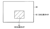
しかしながら、非特許文献1に記載の表示装置では、画面全体を2次元表示モードと3次元表示モードとに切り替える方式であるため、構造的に、部分的な3次元表示を行うことができないものとなっている。このため、例えば図8に示したように、1つの画面60内で、あるエリアを部分的に3次元表示エリア61とし、他のエリアは2次元表示エリア62とするような表示方法は実現できない。このような部分的な3次元表示を行うためには、3次元表示用の光学デバイス自体を構造的に、部分的に2次元表示モードと3次元表示モードとに切り替え可能な構成にしなければならない。
However, in the display device described in Non-Patent Document 1, since the entire screen is switched between the two-dimensional display mode and the three-dimensional display mode, it is structurally impossible to perform partial three-dimensional display. It has become. For this reason, for example, as shown in FIG. 8, a display method in which one area is partially set as a three-
また、2次元表示装置側での映像表示を2次元表示モードと3次元表示モードとで、部分的に適切に切り替える必要がある。3次元表示を行う場合には、2次元表示装置における複数の画素を3次元表示としての1画素に含めるため、2次元表示モードに比べて表示解像度が低下する。3次元表示モードでの表示解像度は、レンチキュラーレンズなどの3次元表示用の光学デバイスの構造に依存する。このため、図8に示した部分的な3次元表示を行う場合に、2次元表示装置の画面全体を3次元表示モードでの表示解像度に合わせてしまうと、2次元表示エリア62での映像表示の画質が本来の2次元表示モードでの映像表示に比べて低下してしまう。また、3次元表示エリア61のエリア設定は、2次元表示装置の画素位置だけでなく、3次元表示用の光学デバイスの構造に応じた位置、サイズにする必要がある。
In addition, it is necessary to appropriately switch the video display on the 2D display device side between the 2D display mode and the 3D display mode. When three-dimensional display is performed, a plurality of pixels in the two-dimensional display device are included in one pixel as the three-dimensional display, so that the display resolution is lower than that in the two-dimensional display mode. The display resolution in the three-dimensional display mode depends on the structure of an optical device for three-dimensional display such as a lenticular lens. For this reason, when the partial 3D display shown in FIG. 8 is performed, if the entire screen of the 2D display device is adjusted to the display resolution in the 3D display mode, the video display in the
本発明はかかる問題点に鑑みてなされたもので、その目的は、2次元表示と3次元表示との部分的な切り替えを容易に行うことができるようにした画像表示装置を提供することにある。 The present invention has been made in view of such problems, and an object thereof is to provide an image display device that can easily perform partial switching between two-dimensional display and three-dimensional display. .
本発明の画像表示装置は、複数の画素を有し、2次元画像データまたは3次元画像データに基づく映像表示を行う2次元表示部と、2次元表示部に対向配置され、2次元表示を行うか3次元表示を行うかに応じて、2次元表示部の各画素からの光線の通過状態を所定サイズの分割エリア単位で部分的、かつ選択的に変化させる3次元表示用光学デバイスとを備えたものである。そして、3次元表示用光学デバイスが、2次元表示を行うエリアでは2次元表示部の各画素からの光線を偏向させずに通過させ、3次元表示を行うエリアでは2次元表示部の各画素からの光線を3次元表示に必要とされる複数の視野角方向に偏向させるよう通過状態を変化させるようになされ、2次元表示部が、2次元表示を行うエリアでは2次元画像データに基づく映像表示を行い、3次元表示を行うエリアでは3次元画像データに基づく映像表示を行うようになされているものである。 An image display device of the present invention has a plurality of pixels, a two-dimensional display unit that performs video display based on two-dimensional image data or three-dimensional image data, and is arranged opposite to the two-dimensional display unit to perform two-dimensional display. Or a three-dimensional display optical device that changes the state of passage of light from each pixel of the two-dimensional display part partially and selectively in units of divided areas of a predetermined size depending on whether to perform three-dimensional display. It is a thing. The optical device for 3D display allows light from each pixel of the 2D display unit to pass without being deflected in an area where 2D display is performed, and from each pixel of the 2D display unit in an area where 3D display is performed. In the area where the two-dimensional display unit performs the two-dimensional display, the video display based on the two-dimensional image data is performed so as to deflect the light beam in the plurality of viewing angle directions required for the three-dimensional display. In an area where 3D display is performed, video display based on 3D image data is performed.
本発明の画像表示装置では、2次元表示部において2次元画像データまたは3次元画像データに基づく映像表示が行われる。3次元表示用光学デバイスでは、2次元表示を行うか3次元表示を行うかに応じて、2次元表示部の各画素からの光線の通過状態を所定サイズの分割エリア単位で部分的、かつ選択的に変化させる。
より具体的には、3次元表示用光学デバイスでは、2次元表示を行うエリアでは2次元表示部の各画素からの光線を偏向させずに通過させ、3次元表示を行うエリアでは2次元表示部の各画素からの光線を3次元表示に必要とされる複数の視野角方向に偏向させるよう通過状態を変化させる。また、2次元表示部では、2次元表示を行うエリアでは2次元画像データに基づく映像表示を行い、3次元表示を行うエリアでは3次元画像データに基づく映像表示を行う。
In the image display device of the present invention, video display based on 2D image data or 3D image data is performed in the 2D display unit. In the optical device for 3D display, the passage state of the light beam from each pixel of the 2D display unit is partially and selectively in units of divided areas depending on whether 2D display or 3D display is performed. Change.
More specifically, in the optical device for three-dimensional display, in the area where two-dimensional display is performed, the light from each pixel of the two-dimensional display unit passes without being deflected, and in the area where three-dimensional display is performed, the two-dimensional display unit The passing state is changed so as to deflect the light rays from the respective pixels in a plurality of viewing angle directions required for three-dimensional display. In the 2D display unit, video display based on 2D image data is performed in an area where 2D display is performed, and video display based on 3D image data is performed in an area where 3D display is performed.
ここで、本発明の画像表示装置は、2次元表示部の画面上において3次元表示を行うエリアを画素単位で指定する指定手段と、指定手段により指定されたエリアの位置およびサイズを、3次元表示用光学デバイスにおける分割エリアを単位とした位置およびサイズに補正する補正手段とをさらに備えていても良い。そして、2次元表示部が、補正手段によって補正されたエリアに3次元画像データに基づく映像表示を行うと共に、その他のエリアでは2次元画像データに基づく映像表示を行うようになされていても良い。また、3次元表示用光学デバイスが、補正手段によって補正されたエリアに対応するエリアを3次元表示を行うエリアとして設定すると共に、その他のエリアは2次元表示を行うエリアとして設定するようになされていても良い。 Here, the image display apparatus according to the present invention includes a designation unit that designates an area for performing the three-dimensional display on the screen of the two-dimensional display unit in units of pixels, and a position and a size of the area designated by the designation unit. The display optical device may further include correction means for correcting the position and size in units of divided areas. The two-dimensional display unit may perform video display based on the three-dimensional image data in the area corrected by the correction unit, and may perform video display based on the two-dimensional image data in other areas. In addition, the optical device for 3D display sets an area corresponding to the area corrected by the correcting means as an area for performing 3D display, and other areas are set as areas for performing 2D display. May be.
このような構成にした場合、指定手段により指定されたエリアの位置およびサイズが、補正手段によって、3次元表示用光学デバイスにおける分割エリアを単位とした位置およびサイズに補正される。2次元表示部では、補正手段によって補正されたエリアに応じて、2次元画像データまたは3次元画像データに基づく映像表示が行われる。3次元表示用光学デバイスでは、補正手段によって補正されたエリアに対応するエリアを3次元表示を行うエリアとして設定し、そのエリアでは2次元表示部の各画素からの光線を、3次元表示に必要とされる複数の視野角方向に偏向させる。
これにより、3次元表示を行うエリアの設定が、2次元表示部側の画素位置だけでなく、3次元表示用光学デバイスの構造に応じた位置、サイズに適切に設定される。また、2次元表示を行うエリアでは2次元表示に適した表示がなされると共に、3次元表示を行うエリアでは3次元表示に適した表示がなされ、2次元表示と3次元表示とのそれぞれに適した表示状態が実現される。
In such a configuration, the position and size of the area specified by the specifying means are corrected by the correcting means to the position and size in units of divided areas in the three-dimensional display optical device. In the two-dimensional display unit, video display based on the two-dimensional image data or the three-dimensional image data is performed according to the area corrected by the correction unit. In the optical device for 3D display, an area corresponding to the area corrected by the correcting means is set as an area for performing 3D display, and the light from each pixel of the 2D display unit is necessary for 3D display in that area. Are deflected in a plurality of viewing angle directions.
Thereby, the setting of the area for performing the three-dimensional display is appropriately set not only at the pixel position on the two-dimensional display unit side but also at a position and a size according to the structure of the optical device for three-dimensional display. In addition, the display suitable for the two-dimensional display is made in the area for performing the two-dimensional display, and the display suitable for the three-dimensional display is made in the area for performing the three-dimensional display. Display state is realized.
本発明の画像表示装置によれば、3次元表示用光学デバイスにおいて、2次元表示を行うか3次元表示を行うかに応じて、2次元表示部の各画素からの光線の通過状態を所定サイズの分割エリア単位で部分的、かつ選択的に変化させるようにしたので、2次元表示と3次元表示との部分的な切り替えを容易に行うことができる。 According to the image display device of the present invention, in the optical device for three-dimensional display, the passage state of the light beam from each pixel of the two-dimensional display unit is set to a predetermined size depending on whether two-dimensional display or three-dimensional display is performed. Since it is changed partially and selectively in units of divided areas, partial switching between the two-dimensional display and the three-dimensional display can be easily performed.
また、本発明の画像表示装置によれば、2次元表示部の画面上において指定された3次元表示を行うエリアの設定を、3次元表示用光学デバイスにおける分割エリアを単位とした位置およびサイズに補正するようにした。これにより、3次元表示を行うエリアの設定を容易かつ適切に行うことができる。また、この場合において、補正手段によって補正されたエリアに応じて、2次元表示部において2次元画像データまたは3次元画像データに基づく映像表示を行い、3次元表示用光学デバイスでは、補正手段によって補正されたエリアに対応するエリアを3次元表示を行うエリアとして設定するようにした。これにより、2次元表示と3次元表示とのそれぞれに適した表示状態を容易に実現することができる。 According to the image display device of the present invention, the setting of the area for performing the specified 3D display on the screen of the 2D display unit is set to the position and size in units of divided areas in the optical device for 3D display. I corrected it. Thereby, it is possible to easily and appropriately set an area for performing the three-dimensional display. In this case, the two-dimensional display unit displays a video based on the two-dimensional image data or the three-dimensional image data in accordance with the area corrected by the correction unit. In the three-dimensional display optical device, the correction unit corrects the image. An area corresponding to the designated area is set as an area for three-dimensional display. Thereby, a display state suitable for each of the two-dimensional display and the three-dimensional display can be easily realized.
以下、本発明の実施の形態について図面を参照して詳細に説明する。 Hereinafter, embodiments of the present invention will be described in detail with reference to the drawings.
[画像表示装置の全体構成]
図1および図2は、本発明の一実施の形態に係る画像表示装置の全体構成の一例を示している。この画像表示装置は、2次元画像データまたは3次元画像データに基づく映像表示を行う2次元表示デバイス10と、この2次元表示デバイス10に対向配置された3次元表示用光学デバイス20とを備えている。この画像表示装置は、例えば図8に示したように、1つの画面60内で、あるエリアを部分的に3次元表示エリア61とし、他のエリアは2次元表示エリア62とするような表示を行うことが可能とされている。図1は、画面全体を2次元表示エリア62とした状態での構成を模式的に示し、図2は、部分的に3次元表示エリア61として部分的に3次元表示にした状態での構成を模式的に示している。
[Overall configuration of image display device]
1 and 2 show an example of the overall configuration of an image display apparatus according to an embodiment of the present invention. The image display device includes a two-
2次元表示デバイス10は、例えば液晶表示ディスプレイで構成され、赤色用画素11R、緑色用画素11G、および青色用画素11Bからなる画素11を複数有し、それら複数の画素11がマトリクス状に配置されている。2次元表示デバイス10は、2次元表示を行うエリアでは2次元画像データに基づく映像表示を行い、3次元表示を行うエリアでは3次元画像データに基づく映像表示を行うようになっている。なお、3次元画像データとは、例えば、3次元表示における複数の視野角方向に対応した複数の視差画像を含むデータである。
本実施の形態において、2次元表示デバイス10が、本発明における「2次元表示部」の一具体例に対応する。
The two-
In the present embodiment, the two-
3次元表示用光学デバイス20は、2次元表示デバイス10に対向する面内で所定サイズの分割エリアがマトリクス状に複数設けられている。それら複数の分割エリアが、例えばアクティブマトリクス方式で駆動されることで、2次元表示を行うか3次元表示を行うかに応じて、2次元表示デバイス10の各画素11からの光線の通過状態を分割エリア単位で部分的、かつ選択的に変化させることが可能に構成されている。より具体的には、複数の分割エリアにはそれぞれ、例えば電圧の印加に応じてレンズ作用が切り替わる切り替え式のマイクロレンズ30が形成されている。すなわち、3次元表示用光学デバイス20には、切り替え式のマイクロレンズ30が2次元表示デバイス10に対向する面内でマトリクス状に複数形成されている。それら複数の切り替え式のマイクロレンズ30が、例えばアクティブマトリクス方式で電圧駆動されることで、2次元表示デバイス10の各画素11からの光線の通過状態を、切り替え式のマイクロレンズ30単位で部分的、かつ選択的に変化させるようになされている。
The three-dimensional display
これにより、3次元表示用光学デバイス20は、2次元表示を行うエリアでは、例えば図1に示したようにマイクロレンズ30による凸レンズの屈折作用がない状態として、2次元表示デバイス10の各画素11からの光線L0,L1,L2を偏向させずにそのままの状態で通過させるようになっている。また、3次元表示を行うエリアでは、例えば図2に示したようにマイクロレンズ30による凸レンズの屈折作用を生じさせることにより、2次元表示デバイス10の各画素11からの光線L1,L2を3次元表示に必要とされる複数の視野角方向に偏向させるようになっている。なお、図2では、1つのマイクロレンズ30に2次元表示デバイス10の画素11が3画素×3画素分割り当てられている例を示している。また、図1および図2では、3次元表示用光学デバイス20の光学作用を分かりやすく説明するため、3次元表示を行うか否かに応じて、3次元表示用光学デバイス20の表面に構造的にマイクロレンズ30が形成されるかのような状態で示している。実際には、後述する図3および図4に示すように、3次元表示用光学デバイス20の内部において、内部的に屈折率が部分的に変化することでマイクロレンズ30によるレンズ作用が生じるような構成とされている。
As a result, the
[3次元表示用光学デバイスの具体的な構成例]
図3は、3次元表示用光学デバイス20の具体的な構成例を示している。図4は、図3に示した3次元表示用光学デバイス20を部分的に3次元表示にした状態を示している。この3次元表示用光学デバイス20は、例えばガラス材料よりなる透明基板21および透明基板22と、それら2つの透明基板21,22の間に挟まれた液晶層23とを備えている。
[Specific configuration example of optical device for three-dimensional display]
FIG. 3 shows a specific configuration example of the three-dimensional display
一方の透明基板21における液晶層23側の表面には、例えばITO(Indium Tin Oxide)膜などの透明な導電膜からなる個別電極24がマトリクス状に複数形成されている。他方の透明基板22における液晶層23側の表面には、例えばITO膜などの透明な導電膜からなる共通電極25がほぼ全面に形成されている。
A plurality of
液晶層23は、例えばレプリカ法(Photoreplication Process)と呼ばれる製造方法で、凹レンズ形状に成型された型に液晶分子31が充填された構成となっている。液晶層23における一方の透明基板21側の面には、配向膜32が平面的に設けられている。液晶層23における他方の透明基板22側には、レプリカ34の型によって凸形状とされた配向膜33が設けられている。すなわち、液晶層23において、下層の平面的な配向膜32と上層の凸形状の配向膜33との間には液晶分子31が充填され、上層のその他の領域はレプリカ34とされている。これにより、液晶層23では液晶分子31が充填された部分が凸形状とされいる。この凸形状とされている部分が、マイクロレンズ30となる部分である。この凸形状の部分は、個別電極24に対応してマトリクス状に複数形成されている。すなわち、マイクロレンズ30となる部分が、個別電極24に対応してマトリクス状に複数形成されている。これにより、以下で説明するように電圧の印加に応じてマイクロレンズ30に凸レンズとしての屈折力が選択的に与えられるようになっている。
The
ここで、上層の共通電極25に印加される共通電圧をVA、下層の複数の個別電極24に印加される所定の駆動電圧をVB1,VB2,VB3,…とする。液晶層23において、形状的にマイクロレンズ30となる部分には、共通電圧と駆動電圧との差の差電圧(VA−VB1),(VA−VB2),(VA−VB3),…が与えられる。液晶分子31は、例えば長手方向と短手方向とで通過光線に対して屈折率の異なる屈折率楕円体の構造を有している。また、液晶分子31は、電圧の印加に応じて分子配列が変わるようになっている。ここで、液晶分子31に差電圧として所定の電圧が与えられた状態での分子配列で与えられる、通過光線に対する屈折率をn0とする。また、差電圧がゼロの状態、すなわち、(VA−VB1)=0,(VA−VB2)=0,(VA−VB3)=0,…での分子配列で与えられる、通過光線に対する屈折率をneとする。また、屈折率の大きさはne>n0の関係とする。レプリカ34の屈折率は、液晶分子31に差電圧として所定の電圧が与えられた状態での低い方の屈折率n0と同じとなるようにする。
Here, it is assumed that a common voltage applied to the upper
これにより、差電圧がゼロの状態では、通過光線に対する液晶分子31の屈折率neとレプリカ34の屈折率とに屈折率差が生じて、マイクロレンズ30が凸レンズとして作用する。これにより、図4に示したように、凸レンズとして作用しているマイクロレンズ30を通過する光線L0,L1,L2が複数の視野角方向に偏向する。一方、差電圧が所定の電圧の状態では、通過光線に対する液晶分子31の屈折率n0とレプリカ34の屈折率とが同じとなり、マイクロレンズ30に相当する部分は凸レンズとして作用しなくなる。これにより、図3に示したように、液晶層23を通過する光線L0,L1,L2は偏向することなく、そのまま透過する。このように、3次元表示用光学デバイス20は、電圧の印加に応じて部分的にレンズ作用を切り替えることができる、切り替え式のマイクロレンズアレイの構成とされている。
Thereby, in a state where the difference voltage is zero, a difference in refractive index occurs between the refractive index ne of the
ところで、この3次元表示用光学デバイス20の駆動電圧の制御は、マイクロレンズ30となる部分が多数存在する場合においては、個々のレンズ部分ごとに配線を与えると高コストになるので、アクティブマトリクス方式で制御することが望ましい。
By the way, the drive voltage of the
図5は、そのアクティブマトリクス方式での駆動回路の配線例を示している。上述したように、マイクロレンズ30となる部分と個別電極24は、互いに対応してマトリクス状に、縦方向(Yi方向)と横方向(Xi方向)に複数形成されている。そのマトリクスの交点部分の個別電極24に、図5に示したようにトランジスタT1を接続する。そして、図5のoutput(Xi,Yi)の電圧を、図3および図4に示した駆動電圧をVB1,VB2,VB3,…として、個別電極24に与える。このようにすることで、例えば図9に示したように3次元表示エリア61が、横方向は座標Xsから座標Xeまで、縦方向は座標Ysから座標Yeまでと定義されたとすると、その座標の領域に所定の駆動電圧を与えることで、容易に3次元表示エリア61にのみレンズ作用を生じさせて3次元表示を行うことができる。
FIG. 5 shows a wiring example of the drive circuit in the active matrix system. As described above, a plurality of portions to be the
[画像表示装置の制御回路を含めた構成]
図7は、制御回路を含めた本実施の形態に係る画像表示装置の構成例を示している。この画像表示装置は、表示装置1と、コントローラ2と、接続ケーブル3と、操作部4とを備えている。表示装置1は、上述の図1〜図4に示した2次元表示デバイス10と3次元表示用光学デバイス20とで構成されている。
本実施の形態において、操作部4が、本発明における「指定手段」の一具体例に対応する。また、コントローラ2が、本発明における「補正手段」の一具体例に対応する。
[Configuration including control circuit of image display device]
FIG. 7 shows a configuration example of the image display apparatus according to this embodiment including the control circuit. The image display device includes a display device 1, a
In the present embodiment, the operation unit 4 corresponds to a specific example of “designating means” in the present invention. The
接続ケーブル3は、表示装置1とコントローラ2とを相互接続するインタフェースであり、例えばHDMI(High Definition Multimedia Interface)規格のケーブルである。接続ケーブル3は、データライン55と、コントロールライン56とを有している。データライン55は、主に表示装置1における2次元表示デバイス10に2次元画像データまたは3次元画像データを伝送するためのものである。データライン55はまた、クロックラインを含んでいる。コントロールライン56は、主にコントローラ2と3次元表示用光学デバイス20との間の制御信号を伝送するためのものである。コントロールライン56は、例えばHDMI規格におけるDDC(Display Data Control Line)に相当する。
The
コントローラ2は、例えばPC(Personal Computer)本体で構成され、2次元画像データ供給部51と、3次元画像データ供給部52と、と、3Dアプリケーション53と、アプリケーションマネージャ54とを備えている。2次元画像データ供給部51は、データライン55を介して2次元表示デバイス10に2次元画像データを供給するものである。3次元画像データ供給部52は、データライン55を介して2次元表示デバイス10に3次元画像データを供給するものである。2次元画像データ供給部51と3次元画像データ供給部52は、例えばHDD(Hard Disk Drive)などの記録媒体を有し、画像データを格納している。なお、コントローラ2の外部から画像データを供給するようにしても良い。
The
操作部4は、例えばマウスなどのポインティングデバイスで構成され。ユーザによって操作されるようになっている。ユーザは、操作部4を介して、2次元表示デバイス10の画面上において3次元表示を行うエリアを画素単位で指定することができるようになっている。
The operation unit 4 is configured by a pointing device such as a mouse. It is operated by the user. The user can designate an area for performing three-dimensional display on the screen of the two-
3Dアプリケーション53およびアプリケーションマネージャ54は、3次元表示に関する表示制御を行うものである。3Dアプリケーション53およびアプリケーションマネージャ54は、例えば、操作部4からの指示に応じて、表示装置1におけるどのエリアを3次元表示を行うエリアに設定するかの制御を行うようになっている。3Dアプリケーション53およびアプリケーションマネージャ54は、後述するように例えば、操作部4を介して指定された3次元表示のエリアの位置およびサイズを、3次元表示用光学デバイス20における分割エリア(マイクロレンズ30)を単位とした位置およびサイズに補正する制御を行うようになっている。
The
[画像表示装置の動作]
次に、本実施の形態に係る画像表示装置の動作を説明する。
[Operation of image display device]
Next, the operation of the image display apparatus according to this embodiment will be described.
この画像表示装置では、2次元表示デバイス10において2次元画像データまたは3次元画像データに基づく映像表示が行われる。3次元表示用光学デバイス20では、2次元表示を行うか3次元表示を行うかに応じて、2次元表示デバイス10の各画素11からの光線の通過状態を所定サイズの分割エリア単位で部分的、かつ選択的に変化させる。より具体的には、3次元表示用光学デバイス20では、2次元表示を行うエリアでは2次元表示デバイス10の各画素11からの光線を偏向させずに通過させる。また、3次元表示を行うエリアでは2次元表示デバイス10の各画素11からの光線を、図2および図4に示したように、3次元表示に必要とされる複数の視野角方向に偏向させるよう通過状態を変化させる。また、2次元表示デバイス10では、2次元表示を行うエリアでは2次元画像データに基づく映像表示を行い、3次元表示を行うエリアでは3次元画像データに基づく映像表示を行う。
In this image display apparatus, the two-
ところで、現在のコンピュータ用ディスプレイデバイスは、最高解像度がディスプレイの画素数により決まっている。一方で、コンピュータの設定として、最高解像度よりも少ない設定の解像度でデータをディスプレイデバイスに送信しても、2次元画像の表示を行う場合には、ディスプレイデバイス側でデータの調整を行うことができている。また通常、2次元表示のアプリケーションウィンドウをディスプレイに表示する場合には、その表示エリアをアナログ的にほぼ自由に設定することが可能である。さらに2次元の動画を表示する場合などデータエリア数が決まっている場合においても、データ開始点の位置はアナログ的に任意の位置を選択することができる。 By the way, the maximum resolution of current computer display devices is determined by the number of pixels of the display. On the other hand, even if data is sent to a display device with a resolution smaller than the maximum resolution as a computer setting, data can be adjusted on the display device side when displaying a two-dimensional image. ing. In general, when a two-dimensional display application window is displayed on the display, the display area can be set almost freely in an analog manner. Further, even when the number of data areas is determined, such as when displaying a two-dimensional moving image, the position of the data start point can be selected in an analog manner.
しかしながら、一般に3次元表示デバイスは、2次元の複数の画素を光学デバイス(光学レンズや遮蔽パターン)の構造に依存する3次元表示としての1画素に含めるため、アナログ的に表示エリアを拡大・縮小することが極めて困難である。つまり、本実施の形態のように部分的に3次元表示が可能である場合においては、3次元表示用光学デバイス20の画素数(マイクロレンズ30の数)に応じた表示エリアサイズになり、2次元表示デバイス10の画素数を基準としたアナログ的な拡大縮小は困難である。さらに、3次元表示のアプリケーションウィンドウを2次元表示デバイス10に表示する場合には、図9に示したようなXs,Xe,Ys,Yeなどの座標を自由に設定することはできない。そして、3次元のデータを表示する場合においてはデータ開始点であるXsおよびYsの位置も任意に設定することはできない。これらの設定は、3次元表示用光学デバイス20の構造に応じた位置、サイズにする必要がある。
However, in general, a three-dimensional display device includes a plurality of two-dimensional pixels in one pixel as a three-dimensional display that depends on the structure of an optical device (optical lens or shielding pattern), so that the display area is enlarged or reduced in an analog manner. It is extremely difficult to do. That is, in the case where partial 3D display is possible as in the present embodiment, the display area size is in accordance with the number of pixels of the 3D display optical device 20 (number of microlenses 30). Analogue scaling based on the number of pixels of the three-
本実施の形態の画像表示装置では、図7に示した操作部4を介して、ユーザが2次元表示デバイス10の画面上において3次元表示を行うエリアを画素単位で指定する。この指定は、2次元表示デバイス10の画面上において2次元画像データに基づく映像表示が行われている状態であっても行うことが可能である。コントローラ2では、その指定されたエリアの位置およびサイズを、3次元表示用光学デバイス20における分割エリア(マイクロレンズ30)を単位とした位置およびサイズに補正する。2次元表示デバイス10では、補正されたエリアに応じて、2次元画像データまたは3次元画像データに基づく映像表示を行う。3次元表示用光学デバイス20では、補正されたエリアに対応するエリアを3次元表示を行うエリアとして設定し、そのエリアでは2次元表示デバイス10の各画素11からの光線を、3次元表示に必要とされる複数の視野角方向に偏向させる。また、その他のエリアは2次元表示を行うエリアとして設定する。これにより、3次元表示を行うエリアの設定が、2次元表示デバイス10側の画素位置だけでなく、3次元表示用光学デバイス20の構造に応じた位置、サイズに適切に設定される。また、2次元表示を行うエリアでは2次元表示に適した表示がなされると共に、3次元表示を行うエリアでは3次元表示に適した表示がなされ、2次元表示と3次元表示とのそれぞれに適した表示状態が実現される。
In the image display apparatus according to the present embodiment, the user designates an area for performing three-dimensional display on the screen of the two-
この3次元表示エリアの補正の動作を、図6を参照してより具体的に説明する。図6は、2次元表示デバイス10における画素11と3次元表示用光学デバイス20における分割エリア(マイクロレンズ30)との対応関係を示している。
The operation of correcting the three-dimensional display area will be described more specifically with reference to FIG. FIG. 6 shows a correspondence relationship between the
まず、操作部4を介して、ユーザが図9に示したようなXs,Xe,Ys,Yeの座標を3次元表示エリア61として指定してきたとする。この場合、コントローラ2では、指定された座標位置とエリアサイズが、3次元表示用光学デバイス20における分割エリア(マイクロレンズ30)を単位とした位置であるかを照会して確認する必要がある。例えば、データ開始点が、図6に示した選択位置42のように、マイクロレンズ30内に入ってしまっている状態にある場合、マイクロレンズ30を単位とした適切な位置に補正する必要がある。ここで、図6において、小さい丸印で示した部分は、2次元表示デバイス10における画素11の境界点の座標を示している。特に、黒く小さい丸印で示した部分はマイクロレンズ30の形成エリアを単位とした3次元表示用グリッド41である。図9に示したような3次元表示エリア61のXs,Xe,Ys,Yeの座標が、この3次元表示用グリッド41の座標となっている必要がある。そこで、図6に示したような選択位置42が指定された場合、その位置を、例えば最も近い位置の3次元表示用グリッド41の座標となるように補正する。
First, it is assumed that the user designates the coordinates of Xs, Xe, Ys, Ye as shown in FIG. 9 as the three-
コントローラ2のアプリケーションマネージャ54は、接続ケーブル3のコントロールライン56を介して、3次元表示用光学デバイス20の構造に関する情報を3次元表示用光学デバイス20から取得すると共に、その取得した情報に基づいて、上記のような位置の補正を行う。コントローラ2のアプリケーションマネージャ54は、3次元表示用光学デバイス20に対して、その補正された位置に基づくエリアを3次元表示を行うエリアとして設定させる。3次元表示用光学デバイス20では、その設定されたエリアにおいて図2および図4に示したようにマイクロレンズ30の屈折作用を生じさせる。アプリケーションマネージャ54はまた、2次元表示デバイス10において、その補正された位置に基づくエリアに3次元画像データに基づく映像表示が行われるような制御を行う。これは、アプリケーションマネージャ54が、3Dアプリケーション53に対して2次元画像データ供給部51からの2次元画像データと、3次元画像データ供給部52からの3次元画像データとを適切に画像処理させることで行われる。この画像処理されて2次元画像データと3次元画像データとが適切に混在した画像データを、データライン55を介して2次元表示デバイス10に供給する。これにより、2次元表示デバイス10では、補正された3次元表示エリア61内に3次元画像データに基づく映像表示がなされ、その他のエリアでは2次元画像データに基づく映像表示がなされる。
The
このように、本実施の形態では、コントローラ2と3次元表示用光学デバイス20との間での制御データの伝送と、コントローラ2と2次元表示デバイス10との間での画像データの伝送とを接続ケーブル3の別々のラインで行っている。これにより、例えば、コントローラ2と2次元表示デバイス10との間で2次元画像データを送信している状態(2次元表示デバイス10で2次元映像を表示している状態)であっても、3次元表示エリアの設定制御を容易に行うことができる。
Thus, in the present embodiment, transmission of control data between the
以上説明したように、本実施の形態に係る画像表示装置によれば、3次元表示用光学デバイス20において、2次元表示を行うか3次元表示を行うかに応じて、2次元表示デバイス10の各画素11からの光線の通過状態を所定サイズの分割エリア単位で部分的、かつ選択的に変化させるようにしたので、2次元表示と3次元表示との部分的な切り替えを容易に行うことができる。
As described above, according to the image display apparatus according to the present embodiment, in the three-dimensional display
また、2次元表示デバイス10の画面上において指定された3次元表示を行うエリアの設定を、3次元表示用光学デバイス20における分割エリア(マイクロレンズ30)を単位とした位置およびサイズに補正するようにした。これにより、3次元表示を行うエリアの設定を容易かつ適切に行うことができる。また、この場合において、補正されたエリアに応じて、2次元表示デバイス10において2次元画像データまたは3次元画像データに基づく映像表示を行い、3次元表示用光学デバイス20では、補正されたエリアに対応するエリアを3次元表示を行うエリアとして設定するようにした。これにより、2次元表示と3次元表示とのそれぞれに適した表示状態を容易に実現することができる。
<その他の実施の形態>
In addition, the setting of the area for performing the three-dimensional display designated on the screen of the two-
<Other embodiments>
本発明は、上記実施の形態に限定されず、その他の変形実施が可能である。
例えば、本発明に適用される3次元表示用光学デバイスは、上記実施の形態で例に挙げたマイクロレンズ30を用いた方式に限らない。例えば、複数のシリンドリカルレンズ(円筒レンズ)を並列配置したレンチキュラーレンズ方式のものであっても構わない。すなわち、図3および図4に示した構造では、切り替え式のマイクロレンズ30がマトリクス状に配置されていたが、これに代えて、切り替え式のシリンドリカルレンズをマトリクス状に配置するようにすれば良い。
The present invention is not limited to the above embodiment, and other modifications can be made.
For example, the optical device for three-dimensional display applied to the present invention is not limited to the method using the
また、上記実施の形態では説明を簡単にするため、3次元表示エリア61が1つのみの場合を例に説明したが、3次元表示エリア61を1つの画面内で2つ以上設けることも可能である。その場合も、3次元表示エリア61に対応するエリアを3次元表示用光学デバイス20によって選択的にレンズ状にすると共に、2次元表示デバイス10の3次元表示エリア61に3次元画像データに基づく映像表示を行えば良い。また、部分的に3次元表示エリア61とする場合に限らず、画面全体を1つの3次元表示エリア61とすることももちろん可能である。
Further, in the above embodiment, the case where there is only one three-
L0,L1,L2…光線、T1…トランジスタ、1…表示装置、2…コントローラ、3…接続ケーブル、4…操作部、10…2次元表示デバイス、11(11R,11G,11B)…画素、20…3次元表示用光学デバイス、21,22…透明基板、23…液晶層、24…個別電極、25…共通電極、30…マイクロレンズ、31…液晶分子、32,33…配向膜、34…レプリカ、41…3次元表示用グリッド、42…選択位置、43…補正位置、51…2次元画像データ供給部、52…3次元画像データ供給部、53…3Dアプリケーション、54…アプリケーションマネージャ、55…データライン、56…コントロールライン、60…表示画面、61…3次元表示エリア、62…2次元表示エリア。
L0, L1, L2 ... light, T1 ... transistor, 1 ... display device, 2 ... controller, 3 ... connection cable, 4 ... operation unit, 10 ... 2D display device, 11 (11R, 11G, 11B) ... pixel, 20 ... Optical device for three-dimensional display, 21, 22 ... Transparent substrate, 23 ... Liquid crystal layer, 24 ... Individual electrode, 25 ... Common electrode, 30 ... Microlens, 31 ... Liquid crystal molecule, 32, 33 ... Alignment film, 34 ... Replica 41 ... 3D display grid, 42 ... selected position, 43 ... correction position, 51 ... 2D image data supply unit, 52 ... 3D image data supply unit, 53 ... 3D application, 54 ... application manager, 55 ...
Claims (5)
前記2次元表示部に対向配置され、2次元表示を行うか3次元表示を行うかに応じて、前記2次元表示部の各画素からの光線の通過状態を所定サイズの分割エリア単位で部分的、かつ選択的に変化させる3次元表示用光学デバイスと
を備え、
前記3次元表示用光学デバイスは、2次元表示を行うエリアでは前記2次元表示部の各画素からの光線を偏向させずに通過させ、3次元表示を行うエリアでは前記2次元表示部の各画素からの光線を3次元表示に必要とされる複数の視野角方向に偏向させるよう通過状態を変化させるようになされ、
前記2次元表示部は、2次元表示を行うエリアでは前記2次元画像データに基づく映像表示を行い、3次元表示を行うエリアでは前記3次元画像データに基づく映像表示を行う
ようになされている画像表示装置。 A two-dimensional display unit having a plurality of pixels and performing video display based on two-dimensional image data or three-dimensional image data;
Depending on whether two-dimensional display or three-dimensional display is performed, the light beam from each pixel of the two-dimensional display unit is partially passed in units of divided areas of a predetermined size. And an optical device for three-dimensional display that selectively changes,
The optical device for three-dimensional display allows light from each pixel of the two-dimensional display unit to pass through without being deflected in an area where two-dimensional display is performed, and each pixel of the two-dimensional display unit in an area where three-dimensional display is performed. The passing state is changed so as to deflect the light beam from a plurality of viewing angle directions required for three-dimensional display,
The two-dimensional display unit displays an image based on the two-dimensional image data in an area for performing two-dimensional display, and performs an image display based on the three-dimensional image data in an area for performing three-dimensional display. Display device.
ようになされている請求項1に記載の画像表示装置。 In the optical device for three-dimensional display, a plurality of the divided areas are provided in a matrix shape in a plane facing the two-dimensional display unit, and the plurality of divided areas are driven by an active matrix method. The image display device according to claim 1, wherein a passage state of light rays from each pixel of the two-dimensional display unit is changed partially and selectively in units of the divided areas.
前記複数の切り替え式のマイクロレンズが、アクティブマトリクス方式で電圧駆動されることで、前記2次元表示部の各画素からの光線の通過状態を前記切り替え式のマイクロレンズ単位で部分的、かつ選択的に変化させる
ようになされている請求項1に記載の画像表示装置。 In the three-dimensional display optical device, a switchable microlens in which a lens action is switched according to voltage application is formed in the divided area, and the switchable microlens is in an in-plane facing the two-dimensional display unit. Are formed in a matrix,
The plurality of switchable microlenses are voltage-driven by an active matrix method, so that the state of passage of light from each pixel of the two-dimensional display portion is partially and selectively in units of the switchable microlenses. The image display device according to claim 1, wherein the image display device is adapted to be changed to:
前記指定手段により指定されたエリアの位置およびサイズを、前記3次元表示用光学デバイスにおける前記分割エリアを単位とした位置およびサイズに補正する補正手段と
をさらに備え、
前記2次元表示部は、前記補正手段によって補正されたエリアに前記3次元画像データに基づく映像表示を行うと共に、その他のエリアでは前記2次元画像データに基づく映像表示を行うようになされ、
前記3次元表示用光学デバイスは、前記補正手段によって補正されたエリアに対応するエリアを3次元表示を行うエリアとして設定すると共に、その他のエリアは2次元表示を行うエリアとして設定する
ようになされている請求項1ないし3のいずれか1項に記載の画像表示装置。 Designating means for designating an area for performing three-dimensional display on the screen of the two-dimensional display unit in units of pixels;
Correction means for correcting the position and size of the area designated by the designation means to a position and size in units of the divided areas in the optical device for three-dimensional display,
The two-dimensional display unit performs video display based on the three-dimensional image data in an area corrected by the correction unit, and performs video display based on the two-dimensional image data in other areas.
The optical device for 3D display sets an area corresponding to the area corrected by the correcting means as an area for performing 3D display, and other areas are set as areas for performing 2D display. The image display device according to any one of claims 1 to 3.
ようになされている請求項4に記載の画像表示装置。 The designation means designates an area for performing the three-dimensional display in a pixel unit of the two-dimensional display unit in a state where video display based on the two-dimensional image data is performed on the screen of the two-dimensional display unit. The image display device according to claim 4, wherein
Priority Applications (1)
| Application Number | Priority Date | Filing Date | Title |
|---|---|---|---|
| JP2008225624A JP5182505B2 (en) | 2008-09-03 | 2008-09-03 | Image display device |
Applications Claiming Priority (1)
| Application Number | Priority Date | Filing Date | Title |
|---|---|---|---|
| JP2008225624A JP5182505B2 (en) | 2008-09-03 | 2008-09-03 | Image display device |
Publications (2)
| Publication Number | Publication Date |
|---|---|
| JP2010060773A true JP2010060773A (en) | 2010-03-18 |
| JP5182505B2 JP5182505B2 (en) | 2013-04-17 |
Family
ID=42187659
Family Applications (1)
| Application Number | Title | Priority Date | Filing Date |
|---|---|---|---|
| JP2008225624A Expired - Fee Related JP5182505B2 (en) | 2008-09-03 | 2008-09-03 | Image display device |
Country Status (1)
| Country | Link |
|---|---|
| JP (1) | JP5182505B2 (en) |
Cited By (8)
| Publication number | Priority date | Publication date | Assignee | Title |
|---|---|---|---|---|
| WO2011117910A1 (en) * | 2010-03-23 | 2011-09-29 | 株式会社 東芝 | Display device and driving method |
| JP2012003072A (en) * | 2010-06-17 | 2012-01-05 | Sony Corp | Lens array element, and image display device |
| JP2012018349A (en) * | 2010-07-09 | 2012-01-26 | Sony Corp | Lens array element, and image display device |
| CN103364959A (en) * | 2012-03-29 | 2013-10-23 | 富士通株式会社 | 3D display device and method |
| CN104049370A (en) * | 2013-03-13 | 2014-09-17 | 株式会社东芝 | Image Display Apparatus |
| US9420267B2 (en) | 2013-12-13 | 2016-08-16 | Samsung Display Co., Ltd. | Display device and liquid crystal lens panel device for the same |
| WO2021166832A1 (en) * | 2020-02-19 | 2021-08-26 | 日東電工株式会社 | Display apparatus and display method |
| WO2021166833A1 (en) * | 2020-02-19 | 2021-08-26 | 日東電工株式会社 | Display apparatus and display method |
Families Citing this family (1)
| Publication number | Priority date | Publication date | Assignee | Title |
|---|---|---|---|---|
| KR102175813B1 (en) | 2014-04-18 | 2020-11-09 | 삼성디스플레이 주식회사 | Three dimensional image display device and method of processing image |
Citations (3)
| Publication number | Priority date | Publication date | Assignee | Title |
|---|---|---|---|---|
| JP2000102038A (en) * | 1998-09-18 | 2000-04-07 | Sanyo Electric Co Ltd | Two-dimensional video image and three-dimensional video image compatible type video display device |
| JP2004258631A (en) * | 2003-02-06 | 2004-09-16 | Toshiba Corp | Stereoscopic picture display device |
| WO2007072289A2 (en) * | 2005-12-20 | 2007-06-28 | Koninklijke Philips Electronics N.V. | Autostereoscopic display device |
-
2008
- 2008-09-03 JP JP2008225624A patent/JP5182505B2/en not_active Expired - Fee Related
Patent Citations (3)
| Publication number | Priority date | Publication date | Assignee | Title |
|---|---|---|---|---|
| JP2000102038A (en) * | 1998-09-18 | 2000-04-07 | Sanyo Electric Co Ltd | Two-dimensional video image and three-dimensional video image compatible type video display device |
| JP2004258631A (en) * | 2003-02-06 | 2004-09-16 | Toshiba Corp | Stereoscopic picture display device |
| WO2007072289A2 (en) * | 2005-12-20 | 2007-06-28 | Koninklijke Philips Electronics N.V. | Autostereoscopic display device |
Cited By (11)
| Publication number | Priority date | Publication date | Assignee | Title |
|---|---|---|---|---|
| WO2011117910A1 (en) * | 2010-03-23 | 2011-09-29 | 株式会社 東芝 | Display device and driving method |
| JP5417529B2 (en) * | 2010-03-23 | 2014-02-19 | 株式会社東芝 | Display device and driving method |
| US8860710B2 (en) | 2010-03-23 | 2014-10-14 | Kabushiki Kaisha Toshiba | Display apparatus and drive method |
| JP2012003072A (en) * | 2010-06-17 | 2012-01-05 | Sony Corp | Lens array element, and image display device |
| JP2012018349A (en) * | 2010-07-09 | 2012-01-26 | Sony Corp | Lens array element, and image display device |
| CN103364959A (en) * | 2012-03-29 | 2013-10-23 | 富士通株式会社 | 3D display device and method |
| US9030737B2 (en) | 2012-03-29 | 2015-05-12 | Fujitsu Limited | 3D display device and method |
| CN104049370A (en) * | 2013-03-13 | 2014-09-17 | 株式会社东芝 | Image Display Apparatus |
| US9420267B2 (en) | 2013-12-13 | 2016-08-16 | Samsung Display Co., Ltd. | Display device and liquid crystal lens panel device for the same |
| WO2021166832A1 (en) * | 2020-02-19 | 2021-08-26 | 日東電工株式会社 | Display apparatus and display method |
| WO2021166833A1 (en) * | 2020-02-19 | 2021-08-26 | 日東電工株式会社 | Display apparatus and display method |
Also Published As
| Publication number | Publication date |
|---|---|
| JP5182505B2 (en) | 2013-04-17 |
Similar Documents
| Publication | Publication Date | Title |
|---|---|---|
| JP5182505B2 (en) | Image display device | |
| JP4967731B2 (en) | Image display device and optical member therefor | |
| JP5963002B2 (en) | Multi-view glassesless stereoscopic image display device and its optimal viewing distance control method | |
| TWI529679B (en) | Autostereoscopic display device | |
| TWI763648B (en) | Autostereoscopic display device and display method | |
| KR100477638B1 (en) | 2D/3D convertible display | |
| US7859484B2 (en) | Three-dimensional display apparatus | |
| US10313662B2 (en) | Glasses-free autostereoscopic 3D display device | |
| US10848752B2 (en) | Method of operating a light field 3D display device having an RGBG pixel structure, and light field 3D display device | |
| JP5176718B2 (en) | Aerial image display device | |
| US10627641B2 (en) | 3D display panel assembly, 3D display device and driving method thereof | |
| CN103096109B (en) | Multiple view automatic stereoscopic displayer and display method | |
| US9995942B2 (en) | Autostereoscopic 3D display device | |
| JP2013045087A (en) | Three-dimensional image display apparatus | |
| US10642061B2 (en) | Display panel and display apparatus | |
| KR20130127496A (en) | 3d display method and 3d display device | |
| KR101975246B1 (en) | Multi view image display apparatus and contorl method thereof | |
| CN103037231B (en) | Display device and electronic equipment | |
| US20130222742A1 (en) | Optical device and image display device | |
| TWI660202B (en) | Naked-eyes type stereoscopic display and stereoscopic image display method thereof | |
| JP2010197917A (en) | Display device | |
| JP2013015711A (en) | Display device | |
| KR20170011048A (en) | Transparent display apparatus and method thereof | |
| JP5318014B2 (en) | 3D display device | |
| US20200021796A1 (en) | Stereo weaving for head-tracked autostereoscopic displays |
Legal Events
| Date | Code | Title | Description |
|---|---|---|---|
| A621 | Written request for application examination |
Free format text: JAPANESE INTERMEDIATE CODE: A621 Effective date: 20110816 |
|
| A977 | Report on retrieval |
Free format text: JAPANESE INTERMEDIATE CODE: A971007 Effective date: 20120829 |
|
| A131 | Notification of reasons for refusal |
Free format text: JAPANESE INTERMEDIATE CODE: A131 Effective date: 20120904 |
|
| A521 | Request for written amendment filed |
Free format text: JAPANESE INTERMEDIATE CODE: A523 Effective date: 20121016 |
|
| TRDD | Decision of grant or rejection written | ||
| A01 | Written decision to grant a patent or to grant a registration (utility model) |
Free format text: JAPANESE INTERMEDIATE CODE: A01 Effective date: 20121219 |
|
| A61 | First payment of annual fees (during grant procedure) |
Free format text: JAPANESE INTERMEDIATE CODE: A61 Effective date: 20130101 |
|
| FPAY | Renewal fee payment (event date is renewal date of database) |
Free format text: PAYMENT UNTIL: 20160125 Year of fee payment: 3 |
|
| LAPS | Cancellation because of no payment of annual fees |