JP2010060284A - Terahertz light detection apparatus and its detection method - Google Patents
Terahertz light detection apparatus and its detection method Download PDFInfo
- Publication number
- JP2010060284A JP2010060284A JP2008222980A JP2008222980A JP2010060284A JP 2010060284 A JP2010060284 A JP 2010060284A JP 2008222980 A JP2008222980 A JP 2008222980A JP 2008222980 A JP2008222980 A JP 2008222980A JP 2010060284 A JP2010060284 A JP 2010060284A
- Authority
- JP
- Japan
- Prior art keywords
- terahertz light
- magnetic field
- current
- gate voltage
- electrode
- Prior art date
- Legal status (The legal status is an assumption and is not a legal conclusion. Google has not performed a legal analysis and makes no representation as to the accuracy of the status listed.)
- Granted
Links
- 238000001514 detection method Methods 0.000 title claims abstract description 61
- 239000004065 semiconductor Substances 0.000 claims abstract description 30
- OKTJSMMVPCPJKN-UHFFFAOYSA-N Carbon Chemical compound [C] OKTJSMMVPCPJKN-UHFFFAOYSA-N 0.000 claims abstract description 26
- 239000002041 carbon nanotube Substances 0.000 claims abstract description 24
- 229910021393 carbon nanotube Inorganic materials 0.000 claims abstract description 24
- 230000005533 two-dimensional electron gas Effects 0.000 claims abstract description 13
- 230000001678 irradiating effect Effects 0.000 claims description 14
- 238000010586 diagram Methods 0.000 description 9
- 238000010521 absorption reaction Methods 0.000 description 7
- 238000000034 method Methods 0.000 description 7
- 239000000758 substrate Substances 0.000 description 7
- 239000010408 film Substances 0.000 description 3
- 239000012535 impurity Substances 0.000 description 3
- 238000005259 measurement Methods 0.000 description 3
- 229910001218 Gallium arsenide Inorganic materials 0.000 description 2
- VYPSYNLAJGMNEJ-UHFFFAOYSA-N Silicium dioxide Chemical compound O=[Si]=O VYPSYNLAJGMNEJ-UHFFFAOYSA-N 0.000 description 2
- 230000007423 decrease Effects 0.000 description 2
- 239000003574 free electron Substances 0.000 description 2
- 239000000463 material Substances 0.000 description 2
- 230000003287 optical effect Effects 0.000 description 2
- 230000035945 sensitivity Effects 0.000 description 2
- 229910052814 silicon oxide Inorganic materials 0.000 description 2
- 239000010409 thin film Substances 0.000 description 2
- RYGMFSIKBFXOCR-UHFFFAOYSA-N Copper Chemical compound [Cu] RYGMFSIKBFXOCR-UHFFFAOYSA-N 0.000 description 1
- XUIMIQQOPSSXEZ-UHFFFAOYSA-N Silicon Chemical compound [Si] XUIMIQQOPSSXEZ-UHFFFAOYSA-N 0.000 description 1
- 230000015572 biosynthetic process Effects 0.000 description 1
- 229910052799 carbon Inorganic materials 0.000 description 1
- 238000004891 communication Methods 0.000 description 1
- 229910052802 copper Inorganic materials 0.000 description 1
- 239000010949 copper Substances 0.000 description 1
- 239000013078 crystal Substances 0.000 description 1
- 230000001419 dependent effect Effects 0.000 description 1
- 239000003814 drug Substances 0.000 description 1
- 238000005516 engineering process Methods 0.000 description 1
- 239000007789 gas Substances 0.000 description 1
- 229910021389 graphene Inorganic materials 0.000 description 1
- SWQJXJOGLNCZEY-BJUDXGSMSA-N helium-3 atom Chemical compound [3He] SWQJXJOGLNCZEY-BJUDXGSMSA-N 0.000 description 1
- 239000012212 insulator Substances 0.000 description 1
- 238000004519 manufacturing process Methods 0.000 description 1
- 239000002184 metal Substances 0.000 description 1
- 229910052751 metal Inorganic materials 0.000 description 1
- 238000011896 sensitive detection Methods 0.000 description 1
- 229910052710 silicon Inorganic materials 0.000 description 1
- 239000010703 silicon Substances 0.000 description 1
- 239000002356 single layer Substances 0.000 description 1
- 238000004611 spectroscopical analysis Methods 0.000 description 1
- 238000001228 spectrum Methods 0.000 description 1
Images


Classifications
-
- H—ELECTRICITY
- H01—ELECTRIC ELEMENTS
- H01L—SEMICONDUCTOR DEVICES NOT COVERED BY CLASS H10
- H01L31/00—Semiconductor devices sensitive to infrared radiation, light, electromagnetic radiation of shorter wavelength or corpuscular radiation and specially adapted either for the conversion of the energy of such radiation into electrical energy or for the control of electrical energy by such radiation; Processes or apparatus specially adapted for the manufacture or treatment thereof or of parts thereof; Details thereof
- H01L31/08—Semiconductor devices sensitive to infrared radiation, light, electromagnetic radiation of shorter wavelength or corpuscular radiation and specially adapted either for the conversion of the energy of such radiation into electrical energy or for the control of electrical energy by such radiation; Processes or apparatus specially adapted for the manufacture or treatment thereof or of parts thereof; Details thereof in which radiation controls flow of current through the device, e.g. photoresistors
- H01L31/10—Semiconductor devices sensitive to infrared radiation, light, electromagnetic radiation of shorter wavelength or corpuscular radiation and specially adapted either for the conversion of the energy of such radiation into electrical energy or for the control of electrical energy by such radiation; Processes or apparatus specially adapted for the manufacture or treatment thereof or of parts thereof; Details thereof in which radiation controls flow of current through the device, e.g. photoresistors characterised by at least one potential-jump barrier or surface barrier, e.g. phototransistors
- H01L31/101—Devices sensitive to infrared, visible or ultraviolet radiation
- H01L31/102—Devices sensitive to infrared, visible or ultraviolet radiation characterised by only one potential barrier or surface barrier
- H01L31/103—Devices sensitive to infrared, visible or ultraviolet radiation characterised by only one potential barrier or surface barrier the potential barrier being of the PN homojunction type
- H01L31/1035—Devices sensitive to infrared, visible or ultraviolet radiation characterised by only one potential barrier or surface barrier the potential barrier being of the PN homojunction type the devices comprising active layers formed only by AIIIBV compounds
-
- H—ELECTRICITY
- H01—ELECTRIC ELEMENTS
- H01L—SEMICONDUCTOR DEVICES NOT COVERED BY CLASS H10
- H01L31/00—Semiconductor devices sensitive to infrared radiation, light, electromagnetic radiation of shorter wavelength or corpuscular radiation and specially adapted either for the conversion of the energy of such radiation into electrical energy or for the control of electrical energy by such radiation; Processes or apparatus specially adapted for the manufacture or treatment thereof or of parts thereof; Details thereof
- H01L31/08—Semiconductor devices sensitive to infrared radiation, light, electromagnetic radiation of shorter wavelength or corpuscular radiation and specially adapted either for the conversion of the energy of such radiation into electrical energy or for the control of electrical energy by such radiation; Processes or apparatus specially adapted for the manufacture or treatment thereof or of parts thereof; Details thereof in which radiation controls flow of current through the device, e.g. photoresistors
- H01L31/10—Semiconductor devices sensitive to infrared radiation, light, electromagnetic radiation of shorter wavelength or corpuscular radiation and specially adapted either for the conversion of the energy of such radiation into electrical energy or for the control of electrical energy by such radiation; Processes or apparatus specially adapted for the manufacture or treatment thereof or of parts thereof; Details thereof in which radiation controls flow of current through the device, e.g. photoresistors characterised by at least one potential-jump barrier or surface barrier, e.g. phototransistors
- H01L31/101—Devices sensitive to infrared, visible or ultraviolet radiation
- H01L31/112—Devices sensitive to infrared, visible or ultraviolet radiation characterised by field-effect operation, e.g. junction field-effect phototransistor
-
- H—ELECTRICITY
- H01—ELECTRIC ELEMENTS
- H01L—SEMICONDUCTOR DEVICES NOT COVERED BY CLASS H10
- H01L29/00—Semiconductor devices adapted for rectifying, amplifying, oscillating or switching, or capacitors or resistors with at least one potential-jump barrier or surface barrier, e.g. PN junction depletion layer or carrier concentration layer; Details of semiconductor bodies or of electrodes thereof ; Multistep manufacturing processes therefor
- H01L29/66—Types of semiconductor device ; Multistep manufacturing processes therefor
- H01L29/68—Types of semiconductor device ; Multistep manufacturing processes therefor controllable by only the electric current supplied, or only the electric potential applied, to an electrode which does not carry the current to be rectified, amplified or switched
- H01L29/76—Unipolar devices, e.g. field effect transistors
- H01L29/772—Field effect transistors
- H01L29/778—Field effect transistors with two-dimensional charge carrier gas channel, e.g. HEMT ; with two-dimensional charge-carrier layer formed at a heterojunction interface
- H01L29/7786—Field effect transistors with two-dimensional charge carrier gas channel, e.g. HEMT ; with two-dimensional charge-carrier layer formed at a heterojunction interface with direct single heterostructure, i.e. with wide bandgap layer formed on top of active layer, e.g. direct single heterostructure MIS-like HEMT
- H01L29/7787—Field effect transistors with two-dimensional charge carrier gas channel, e.g. HEMT ; with two-dimensional charge-carrier layer formed at a heterojunction interface with direct single heterostructure, i.e. with wide bandgap layer formed on top of active layer, e.g. direct single heterostructure MIS-like HEMT with wide bandgap charge-carrier supplying layer, e.g. direct single heterostructure MODFET
Abstract
Description
本発明は、微弱なテラヘルツ光の強度と周波数を検出するテラヘルツ光検出装置とその検出方法に関する。 The present invention relates to a terahertz light detection device that detects the intensity and frequency of weak terahertz light and a detection method thereof.
本発明において、「テラヘルツ光」とは周波数が1〜10THz(1THz=1012Hz)の領域、すなわち波長が0.03mm〜0.3mmのサブミリ波から遠赤外線領域の電磁波を意味する。 In the present invention, “terahertz light” means an electromagnetic wave in a frequency range of 1 to 10 THz (1 THz = 10 12 Hz), that is, a submillimeter wave having a wavelength of 0.03 mm to 0.3 mm to a far infrared region.
テラヘルツ光は、電波天文学、材料科学、生体分子分光学などの基礎学術分野からセキュリティ、情報通信、環境、医療などの実用分野に至る幅広い分野での応用が期待されている。 Terahertz light is expected to be applied in a wide range of fields from basic academic fields such as radio astronomy, material science, and biomolecule spectroscopy to practical fields such as security, information communication, environment, and medicine.
しかし、テラヘルツ光は、赤外線、可視光、紫外線などの光(周波数1013〜1015Hz)と電波(周波数103〜1012Hz)の間に挟まれた周波数帯域の電磁波であり、光学と電子工学という既存の技術がそのままでは適用できない問題点がある。
However, terahertz light is an electromagnetic wave in a frequency band sandwiched between light (
テラヘルツ光を検出する検出器は、種々のものが既に提案されている。そのうち、テラヘルツ光の強度が数fW(10−15W)の非常に微弱なテラヘルツ光を検出できる検出器として、非特許文献1,2が既に報告されている。
また、テラヘルツ光の周波数を検出できる検出器として、特許文献1が既に提案されている。
Various detectors for detecting terahertz light have already been proposed. Among them,
非特許文献1は、表面にシリコン酸化膜があるシリコン基板上のカーボンナノチューブによりテラヘルツ光を検出するものである。
非特許文献2は、超伝導を用いたテラヘルツ光検出器である。
Non-Patent
Non-Patent
特許文献1は、周波数分解の良い測定においてS/N比の良いスペクトルを得ることを目的とする。
そのため、特許文献1の検出器本体51は、図9に示すように、基板53と、基板53の+Z側の面に形成された光スイッチ素子による検出素子部(金属膜55,56間の間隔gの部分)と、を有する。基板53と略同じ屈折率を有する部材60が、基板53の−Z側に、部材60の−Z側の面と基板53の+Z側の面との間にテラヘルツパルス光の反射面を形成しないように、設けられる。部材60の−Z側の面の形状及び部材60の厚さは、部材60の−Z側の面の所定領域から入射して間隔gの領域(有効領域)の付近に集光したテラヘルツ光のうち、基板53の+Z側の面で反射された光が、最初に部材60の−Z側の面で反射した後に、間隔gの領域に実質的に入射しないかあるいは更に2回以上反射した後にのみ間隔gの領域に入射するように、設定される。
Therefore, as shown in FIG. 9, the detector
非特許文献1のテラヘルツ光検出器は、シリコン酸化膜中の不純物準位に捕獲されている電子のテラヘルツ応答を用いる。そのため検出器作製の際に、不純物に対して所望の位置にカーボンナノチューブを配置することができない。また、不純物準位にはシャープな波長選択性がないため、テラヘルツ光の周波数測定ができない。
The terahertz photodetector of Non-Patent
非特許文献2のテラヘルツ光検出器は、高感度性を得るのに0.3〜0.4Kの極低温を必要とするため、高価で大規模なヘリウム3クライオスタットを使用しなければならない。
Since the terahertz photodetector of Non-Patent
特許文献1のテラヘルツ光検出器は、部材20によりテラヘルツ光が吸収されるので、強度が数fW(10−15W)の非常に微弱なテラヘルツ光の検出はできない。
The terahertz light detector of
本発明は、上述した問題点を解決するために創案されたものである。すなわち本発明の目的は、極低温を必要することなく、小規模の装置で、非常に微弱なテラヘルツ光の強度を明確に検出でき、かつその周波数を正確に測定することができるテラヘルツ光検出装置とその検出方法を提供することにある。 The present invention has been developed to solve the above-described problems. That is, an object of the present invention is to provide a terahertz light detecting device capable of clearly detecting the intensity of very weak terahertz light and accurately measuring the frequency thereof with a small-scale device without requiring extremely low temperatures. And providing a detection method thereof.
本発明によれば、表面から一定の位置に2次元電子ガスが形成された半導体チップと、
該半導体チップの表面に密着して設けられたカーボンナノチューブ、導電性のソース電極、ドレイン電極及びゲート電極とを備え、
前記カーボンナノチューブは、半導体チップの表面に沿って延び、かつその両端部がソース電極とドレイン電極に接続され、
前記ゲート電極は、カーボンナノチューブの側面から一定の間隔を隔てて位置し、
さらに、前記ソース電極とドレイン電極の間に所定の電圧を印加し、その間のSD電流を検出するSD電流検出回路と、
前記ソース電極とゲート電極の間に可変ゲート電圧を印加するゲート電圧印加回路と、
前記半導体チップに可変磁場を印加する磁場発生装置と、を備えることを特徴とするテラヘルツ光検出装置が提供される。
According to the present invention, a semiconductor chip in which a two-dimensional electron gas is formed at a certain position from the surface;
Carbon nanotubes provided in close contact with the surface of the semiconductor chip, a conductive source electrode, a drain electrode and a gate electrode,
The carbon nanotube extends along the surface of the semiconductor chip, and both ends thereof are connected to the source electrode and the drain electrode,
The gate electrode is located at a certain distance from the side surface of the carbon nanotube,
An SD current detection circuit for applying a predetermined voltage between the source electrode and the drain electrode and detecting an SD current therebetween;
A gate voltage application circuit for applying a variable gate voltage between the source electrode and the gate electrode;
There is provided a terahertz light detection device comprising a magnetic field generation device that applies a variable magnetic field to the semiconductor chip.
本発明の好ましい実施形態によれば、前記SD電流検出回路、ゲート電圧印加回路及び磁場発生装置を制御し、かつ前記SD電流、ゲート電圧及び磁場値からテラヘルツ光の周波数と強度を演算する検出制御装置を備える。 According to a preferred embodiment of the present invention, detection control for controlling the SD current detection circuit, the gate voltage application circuit, and the magnetic field generator, and calculating the frequency and intensity of the terahertz light from the SD current, gate voltage, and magnetic field value Equipment.
前記検出制御装置により、テラヘルツ光を照射しながら、SD電流のゲート電圧と磁場に対する依存性を測定し、SD電流のピークがゲート電圧に対して最も大きくシフトする時の磁場値を検出し、この磁場値からテラヘルツ光の周波数を求める。 The detection control device measures the dependence of the SD current on the gate voltage and the magnetic field while irradiating the terahertz light, and detects the magnetic field value when the peak of the SD current is the largest shift with respect to the gate voltage. The frequency of terahertz light is obtained from the magnetic field value.
また、前記検出制御装置により、ゲート電圧に対してSD電流のピークが最も大きくシフトする時の磁場値とゲート電圧に固定し、テラヘルツ光を照射しながら、SD電流の時間変化を測定する。 Further, the detection control device fixes the magnetic field value and the gate voltage when the peak of the SD current shifts the most with respect to the gate voltage, and measures the time change of the SD current while irradiating terahertz light.
また本発明によれば、表面から一定の位置に2次元電子ガスが形成された半導体チップと、
該半導体チップの表面に密着して設けられたカーボンナノチューブ、導電性のソース電極、ドレイン電極及びゲート電極とを備え、
前記カーボンナノチューブは、半導体チップの表面に沿って延び、かつその両端部がソース電極とドレイン電極に接続され、
ゲート電極は、カーボンナノチューブの側面から一定の間隔を隔てて位置し、
さらに、前記ソース電極とドレイン電極の間に所定の電圧を印加しその間のSD電流を検出するSD電流検出回路と、
前記ソース電極とゲート電極の間に可変ゲート電圧を印加するゲート電圧印加回路と、
前記半導体チップに可変磁場を印加する磁場発生装置とを備えるテラヘルツ光検出装置を準備し、
テラヘルツ光を照射しながら、SD電流のゲート電圧と磁場に対する依存性を測定し、SD電流のピークがゲート電圧に対して最も大きくシフトする時の磁場値を検出し、この磁場値からテラヘルツ光の周波数を求める、ことを特徴とするテラヘルツ光検出方法が提供される。
According to the present invention, a semiconductor chip in which a two-dimensional electron gas is formed at a certain position from the surface;
Carbon nanotubes provided in close contact with the surface of the semiconductor chip, a conductive source electrode, a drain electrode and a gate electrode,
The carbon nanotube extends along the surface of the semiconductor chip, and both ends thereof are connected to the source electrode and the drain electrode,
The gate electrode is located at a certain distance from the side surface of the carbon nanotube,
An SD current detection circuit for applying a predetermined voltage between the source electrode and the drain electrode and detecting an SD current therebetween;
A gate voltage application circuit for applying a variable gate voltage between the source electrode and the gate electrode;
Preparing a terahertz light detecting device comprising a magnetic field generating device for applying a variable magnetic field to the semiconductor chip;
While irradiating terahertz light, the dependence of the SD current on the gate voltage and the magnetic field is measured, and the magnetic field value when the peak of the SD current shifts the most with respect to the gate voltage is detected. There is provided a terahertz light detection method characterized by obtaining a frequency.
本発明の好ましい実施形態によれば、ゲート電圧に対してSD電流のピークが最も大きくシフトする時の磁場値とゲート電圧に固定し、テラヘルツ光を照射しながら、SD電流の時間変化を測定する。 According to a preferred embodiment of the present invention, the magnetic field value and the gate voltage when the SD current peak shifts the most with respect to the gate voltage are fixed, and the time variation of the SD current is measured while irradiating terahertz light. .
上記本発明の構成によれば、テラヘルツ光を照射することで、ゲート電圧に対するSD電流のピーク(クーロンピーク)が正のゲート電圧側にシフトし、このシフト(クーロンピークシフト)が最大となる磁場から、テラヘルツ光の周波数を求めることができることが、後述する温度2.5Kの試験結果から確認された。
また、ゲート電圧に対してSD電流のピークが最も大きくシフトする時の磁場値とゲート電圧に固定することにより、例えばフォトン1つのテラヘルツ光1でさえも検出できることが、後述する温度2.5Kの試験結果から確認された。
従って、本発明の装置及び方法によれば、0.3〜0.4Kの極低温を必要することなく、小規模の装置で、数fW(10−15W)の非常に微弱なテラヘルツ光の強度を明確に検出でき、かつその周波数を正確に測定することができる。
According to the configuration of the present invention described above, irradiation with terahertz light shifts the SD current peak (Coulomb peak) with respect to the gate voltage to the positive gate voltage side, and the magnetic field that maximizes this shift (Coulomb peak shift). From this, it was confirmed from the test result at a temperature of 2.5 K described later that the frequency of the terahertz light can be obtained.
Further, by fixing the magnetic field value and the gate voltage when the SD current peak shifts the most with respect to the gate voltage, it is possible to detect, for example, even one
Therefore, according to the apparatus and method of the present invention, a very small terahertz light of several fW (10 −15 W) can be obtained with a small-scale apparatus without requiring a cryogenic temperature of 0.3 to 0.4 K. The intensity can be clearly detected and the frequency can be accurately measured.
以下、本発明の好ましい実施形態を図面を参照して説明する。なお、各図において、共通する部分には同一の符号を付し重複した説明を省略する。 Hereinafter, preferred embodiments of the present invention will be described with reference to the drawings. In each figure, common portions are denoted by the same reference numerals, and redundant description is omitted.
図1は、本発明で使用する高電子移動度トランジスタ(HEMT)の説明図である。
HEMT(High Electron Mobility Transistor:高電子移動度トランジスタ)は、2次元電子ガス(「2DEG」と略称する)を利用したトランジスタであり、変調ドープにより、2次元電子ガスが形成され、電子移動度が高い特徴がある。従って、ソースからドレインに流れる電子電流を、高い電子移動度を利用して高速に制御することができる。
なお「2次元電子ガス」とは、半導体と絶縁体あるいは異種半導体どうしの接合界面で界面に沿って運動する電子、すなわち、2次元平面にのみ運動量をもつ希薄な電子をいう。
FIG. 1 is an explanatory diagram of a high electron mobility transistor (HEMT) used in the present invention.
A HEMT (High Electron Mobility Transistor) is a transistor that uses a two-dimensional electron gas (abbreviated as “2DEG”). A two-dimensional electron gas is formed by modulation doping, and the electron mobility is increased. There are high features. Therefore, the electron current flowing from the source to the drain can be controlled at high speed using high electron mobility.
Note that the “two-dimensional electron gas” refers to an electron that moves along an interface between a semiconductor and an insulator or a heterogeneous semiconductor, that is, a rare electron that has a momentum only in a two-dimensional plane.
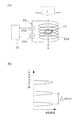
図2は、本発明によるテラヘルツ光検出装置の構成図である。この図において、(A)はテラヘルツ光検出装置の断面図、(B)は(A)のB−B矢視図(平面図)である。
この図に示すように、本発明のテラヘルツ光検出装置10は、半導体チップ12、カーボンナノチューブ14、ソース電極15、ドレイン電極16、ゲート電極17、SD電流検出回路18、ゲート電圧印加回路19、および磁場発生装置20を備える。
FIG. 2 is a configuration diagram of a terahertz light detection device according to the present invention. In this figure, (A) is a cross-sectional view of the terahertz light detection device, and (B) is a BB arrow view (plan view) of (A).
As shown in this figure, the terahertz
半導体チップ12は、表面から一定の位置(距離)に2次元電子ガス13が形成された高電子移動度トランジスタ(HEMT)である。なお、図1におけるゲート、ソース及びドレインがないHEMTをここでは半導体チップ12と呼ぶ。
2次元電子ガス13の表面からの距離は、後述の実施例では約60nmであるが、60nm未満でも60nm以上でもよい。
The
The distance from the surface of the two-
カーボンナノチューブ14は、炭素によって作られる六員環ネットワーク(グラフェンシート)が単層又は多層の同軸管状になった物質である。かかるカーボンナノチューブ14は、銅の1000倍以上の高電流密度耐性を有しており、テラヘルツ光1による少数個の光子により長さ方向の電流が大きく変化する特性を有し、検出部として2次元電子ガス13よりも高い高感度検出が可能である。
カーボンナノチューブ14は、後述する実施例では、長さが600nmであり、半導体チップ12の表面に密着し表面に沿って延び、その両端部がソース電極15とドレイン電極16に接続されている。
The
The
ソース電極15及びドレイン電極16は、1本のカーボンナノチューブ14を挟んでその長さ方向外側に間隔を開けて位置し、半導体チップ12の表面に密着して設けられる。また、この例ではソース電極15は接地され、0Vに保持される。
なお後述の実施例において、ソース電極15及びドレイン電極16は、Ti/Auの薄膜である。
The
In the examples described later, the
ゲート電極17は、カーボンナノチューブ14の側面から一定の間隔(後述する実施例では、500nm)を隔てて位置し、半導体チップ12の表面に密着して設けられる。
後述の実施例において、ゲート電極17は、Ti/Auの薄膜である。
The
In the embodiments described later, the
SD電流検出回路18は、ソース電極15とドレイン電極16を電気的に接続する導電線18aと、導電線18aの途中に設けられた直流電源18b及び電流計18cとからなる。直流電源18bはソース電極15とドレイン電極16の間にドレイン電極16をプラス(+)とする所定の電圧を印加する。また、電流計18cはソース電極15とドレイン電極16の間に流れる電流(以下、「ソース−ドレイン電流」または「SD電流」と呼ぶ)を検出する。所定の電圧は後述の実施例では1.5mVである。
また、電流計18cには、ノイズカットフィルター18dが着脱可能に取り付けられており、電流計18cの出力信号から変動の激しいノイズを除去するようになっている。
The SD
In addition, a noise cut
ゲート電圧印加回路19は、ソース電極15とゲート電極17を電気的に接続する導電線19aと、導電線19aの途中に設けられた直流電源19bとからなる。直流電源19bはソース電極15とゲート電極17の間にゲート電極17をマイナス(−)とする可変ゲート電圧を印加する。以下、ソース電極15とゲート電極17の間の電圧を「ゲート電圧」と呼ぶ。
The gate
図3は、図2の磁場発生装置の模式図(A)とテラヘルツ光検出原理の説明図(B)である。
図3(A)に示すように、磁場発生装置20は、半導体チップ12に入射するテラヘルツ光1の光軸を囲むコイル20aと、コイル20aの両端に所定の電圧を印加する直流電源20bと、コイル20aを流れる電流(以下、「コイル電流」と呼ぶ)を表示する電流計20cとからなり、半導体チップ12に磁場Bを印加する。なお、実際の測定では、所定の電流値を入力して流し、コイルにかかる電圧が検出される。
磁場Bは、コイル電流から一義的に求めることができる。
FIG. 3 is a schematic diagram (A) of the magnetic field generator of FIG. 2 and an explanatory diagram (B) of the terahertz light detection principle.
As shown in FIG. 3A, the
The magnetic field B can be uniquely determined from the coil current.
図3(B)は、磁場印加によるランダウ準位の形成を示す図である。この図において、横軸は状態密度、縦軸は電子のエネルギーである。
この図に示すように、照射する電磁波の光子エネルギーhfがランダウ準位のエネルギー間隔(h/2π)eB/m*・・・(1)と等しい時、電磁波の非常に大きな吸収が生じる。この現象はサイクロトロン吸収あるいはサイクロトロン共鳴と呼ばれる。
ここで、hはプランク定数、eは電荷素量、Bは磁場、m*は結晶中の電子の有効質量(例えばGaAsならば、自由電子の質量の0.0665倍)である。
FIG. 3B is a diagram showing formation of Landau levels by applying a magnetic field. In this figure, the horizontal axis represents the density of states, and the vertical axis represents the energy of electrons.
As shown in this figure, when the photon energy hf of the radiated electromagnetic wave is equal to the Landau level energy interval (h / 2π) eB / m * (1), very large absorption of the electromagnetic wave occurs. This phenomenon is called cyclotron absorption or cyclotron resonance.
Here, h is the Planck constant, e is the elementary charge, B is the magnetic field, and m * is the effective mass of electrons in the crystal (for example, 0.0665 times the mass of free electrons in GaAs).
サイクロトロン吸収が生じる際のテラヘルツ光の光子エネルギーhfは、サイクロトロン吸収が生じる際のランダウ準位のエネルギー間隔に等しくなる。
すなわち、hf=(h/2π)eB/m*・・・(2)が成り立つ。
この式から磁場B以外のh,e,m*は既知の定数であるので、サイクロトロン吸収が生じる際の磁場Bからテラヘルツ光の周波数fを求めることができる。
本発明のテラヘルツ光検出装置10では、2次元電子ガス13のサイクロトロン吸収を利用する。
The photon energy hf of the terahertz light when cyclotron absorption occurs is equal to the energy interval of the Landau level when cyclotron absorption occurs.
That is, hf = (h / 2π) eB / m * (2) holds.
Since h, e, and m * other than the magnetic field B are known constants from this equation, the frequency f of the terahertz light can be obtained from the magnetic field B when cyclotron absorption occurs.
The terahertz
図2及び図3において、本発明のテラヘルツ光検出装置10は、さらに検出制御装置22を備える。検出制御装置22は、例えばコンピュータ(PC)であり、SD電流検出回路18、ゲート電圧印加回路19及び磁場発生装置20を制御し、かつSD電流、ゲート電圧及び磁場値からテラヘルツ光の周波数と強度を演算する機能を有する。
この検出制御装置22により、テラヘルツ光1を照射しながら、SD電流のゲート電圧と磁場に対する依存性を測定し、SD電流のピークがゲート電圧に対して最も大きくシフトする時の磁場値を検出し、この磁場値からテラヘルツ光の周波数を求める。
また、この検出制御装置22により、ゲート電圧に対してSD電流のピークが最も大きくシフトする時の磁場値とゲート電圧に固定し、テラヘルツ光を照射しながら、SD電流の時間変化を測定する。
2 and 3, the terahertz
The
Also, the
上述した本発明によるテラヘルツ光検出装置を用い、温度を2.5K、ドレイン電極16に1.5mVの電圧を印加し、数fW(10−15W)の非常に微弱なテラヘルツ光1を照射した。なおこの試験では、電流計18cにノイズカットフィルター18dを取り付け、変動の激しいノイズを除去した。
Using the above-described terahertz light detection apparatus according to the present invention, a temperature of 2.5 K, a voltage of 1.5 mV was applied to the
図4は、1.6THzのテラヘルツ光1を検出した試験結果である。各図において、横軸はゲート電圧(V)であり、縦軸はソース−ドレイン電流(pA)である。
FIG. 4 shows test results obtained by detecting 1.6
図4において、各データの右端に記載した数字は、磁場B(T)の強度である。また各データは、図面の明瞭化のため、上下にシフトして記載しており、各データの水平部は0(pA)である。
この図から、磁場Bが0に対し、磁場Bが3.95(T)までは、各データの信号検出位置が右方にシフトし、3.95(T)で最大となり、それ以上では7.85(T)までシフト量が徐々に小さくなっている。
すなわち、図4からテラヘルツ光1を照射することで、クーロンピークが正のゲート電圧側にシフトしている様子が見て取れる。また、ピークシフトの大きさ(ゲート電圧差)は、デバイスに垂直に印加した磁場Bに強く依存しており、3.95Tで最大になっている。
In FIG. 4, the number described at the right end of each data is the intensity of the magnetic field B (T). In addition, each data is illustrated as being shifted up and down for clarity of the drawing, and the horizontal portion of each data is 0 (pA).
From this figure, when the magnetic field B is 0 and the magnetic field B is up to 3.95 (T), the signal detection position of each data shifts to the right and becomes the maximum at 3.95 (T), and beyond that, 7 The shift amount gradually decreases to .85 (T).
That is, it can be seen from FIG. 4 that the coulomb peak is shifted to the positive gate voltage side by irradiating the
このシフト(クーロンピークシフトと呼ぶ)の大きさは、検出されたテラヘルツ光の2次元電子ガス13による吸収効率に比例すると考えられる。すなわち、クーロンピークシフトが最大となる磁場Bは、照射したテラヘルツ光1の波長184μm(1.6THz)とGaAs中の電子の有効質量0.0665m0(m0:自由電子の質量)から導出されるサイクロトロン共鳴時の値と一致している。
従って、クーロンピークシフトが最大となる磁場B(この例では3.95(T))から、式(2)によりテラヘルツ光の周波数fを求めることができる。
The magnitude of this shift (referred to as Coulomb peak shift) is considered to be proportional to the absorption efficiency of the detected terahertz light by the two-
Therefore, from the magnetic field B (3.95 (T) in this example) that maximizes the Coulomb peak shift, the frequency f of the terahertz light can be obtained by Equation (2).
図5は、2.5THzのテラヘルツ光1を検出した試験結果である。この例では、磁場Bが0に対し、磁場Bが6.13(T)までは、各データの信号検出位置が右方にシフトし、6.13(T)で最大となり、それ以上では7.85(T)までシフト量が徐々に小さくなっている。
FIG. 5 shows the test results of detecting 2.5
図4と図5からテラヘルツ光1の波長を変えると、ピークシフトが最大となる磁場もそれに比例して変化することが分かった。以上の事実は、2DEG中でテラヘルツ光1で励起されたキャリアを、間近にあるCNTがエレクトロメータとして読み取っていることを意味する。
4 and 5, it is found that when the wavelength of the
上述した本発明によるテラヘルツ光検出装置を用い、温度を2.5K、ドレイン電極16に1.5mVの電圧を印加し、数fW(10−15W)の非常に微弱なテラヘルツ光1を照射した。なおこの試験では、電流計18cからノイズカットフィルター18dを取り外した。
また、1.6THzのテラヘルツ光1を照射し、磁場Bは、クーロンピークシフトが最大となる3.95(T)に固定した。また、ゲート電圧は、クーロンピークシフト位置(この例では−1.41V)に固定した。
Using the above-described terahertz light detection apparatus according to the present invention, a temperature of 2.5 K, a voltage of 1.5 mV was applied to the
In addition, 1.6
図6は、本発明のテラヘルツ光検出装置による1.6THzのテラヘルツ光1の検出結果である。この図において、横軸は時間、縦軸は電流(ソース−ドレイン電流)である。
この図から、テラヘルツ光1が非常に微弱にもかかわらず、テラヘルツ光1の照射(THz on)時に、検出データが上下に激しく変動している。この電流の揺らぎは、少数個のフォトンを検出していることを示している。このことから、本発明のテラヘルツ光検出装置により、非常に微弱なテラヘルツ光1、例えばフォトン1つのテラヘルツ光1でさえも検出できることがわかる。
FIG. 6 shows the detection result of 1.6
From this figure, although the
図7は、本発明によるテラヘルツ光検出方法のフロー図である。この図は、上述したテラヘルツ光検出装置を用いてテラヘルツ光1の周波数を求める方法を示している。
テラヘルツ光1の周波数を求める場合に、本発明の方法では、電流計18cにノイズカットフィルター18dを挿入し(S1)、テラヘルツ光1を照射しながら(S2)、ソース−ドレイン電流(SD電流)のゲート電圧と磁場に対する依存性を測定する(S3〜S5)。
次いで、SD電流のピークがゲート電圧に対して最も大きくシフトする時の磁場値Bを検出する(S6〜S7)。
この磁場値Bを上述した式(2)に代入することで、テラヘルツ光1の周波数fを求めることができる(S8)。
FIG. 7 is a flowchart of the terahertz light detection method according to the present invention. This figure shows a method for obtaining the frequency of the
When obtaining the frequency of the
Next, the magnetic field value B when the SD current peak shifts the most with respect to the gate voltage is detected (S6 to S7).
By substituting this magnetic field value B into the above-described equation (2), the frequency f of the
図8は、本発明によるテラヘルツ光検出方法の別のフロー図である。この図は、上述したテラヘルツ光検出装置を用いて数fW(10−15W)の非常に微弱なテラヘルツ光1を検出する方法を示している。
微弱なテラヘルツ光1を検出する場合に、本発明の方法では、電流測定系からノイズカットのためのフィルターを取り去り(S11)、クーロンピークシフトが最大となる磁場値Bに固定し(S12)、ゲート電圧をテラヘルツ光1を照射した時の電流ピークに相当する位置に固定し(S13)、テラヘルツ光1を照射しながら(S14)、ソース−ドレイン電流(SD電流)の時間変化を測定する(S15)。
この方法によりテレグラフ的な電流のスイッチングを観測することで、少数個の光子を検出することができ、高感度検出が可能となる。
FIG. 8 is another flowchart of the terahertz light detection method according to the present invention. This figure shows a method for detecting a very
When detecting the
By observing telegraph-like current switching by this method, a small number of photons can be detected, and highly sensitive detection is possible.
上述した本発明の構成によれば、テラヘルツ光を照射することで、ゲート電圧に対するSD電流のピーク(クーロンピーク)が正のゲート電圧側にシフトし、このシフト(クーロンピークシフト)が最大となる磁場から、テラヘルツ光の周波数を求めることができることが、温度2.5Kの試験結果から確認された。
また、また、ゲート電圧に対してSD電流のピークが最も大きくシフトする時の磁場値とゲート電圧に固定することにより、例えばフォトン1つのテラヘルツ光1でさえも検出できることが、温度2.5Kの試験結果から確認された。
従って、本発明の装置及び方法によれば、0.3〜0.4Kの極低温を必要することなく、小規模の装置で、数fW(10−15W)の非常に微弱なテラヘルツ光の強度を明確に検出でき、かつその周波数を正確に測定することができる。
According to the configuration of the present invention described above, by irradiating terahertz light, the peak of the SD current (Coulomb peak) with respect to the gate voltage is shifted to the positive gate voltage side, and this shift (Coulomb peak shift) is maximized. It was confirmed from the test result at a temperature of 2.5 K that the frequency of the terahertz light can be obtained from the magnetic field.
Further, by fixing the magnetic field value and the gate voltage when the SD current peak shifts the most with respect to the gate voltage, it is possible to detect, for example, even one
Therefore, according to the apparatus and method of the present invention, a very small terahertz light of several fW (10 −15 W) can be obtained with a small-scale apparatus without requiring a cryogenic temperature of 0.3 to 0.4 K. The intensity can be clearly detected and the frequency can be accurately measured.
なお、本発明は上述した実施例及び実施形態に限定されず、本発明の要旨を逸脱しない範囲で種々変更できることは勿論である。 In addition, this invention is not limited to the Example and embodiment mentioned above, Of course, it can change variously in the range which does not deviate from the summary of this invention.
1 テラヘルツ光、
10 テラヘルツ光検出装置、
12 半導体チップ(HEMT)、13 2次元電子ガス(2DEG)、
14 カーボンナノチューブ、15 ソース電極、16 ドレイン電極、
17 ゲート電極、18SD電流検出回路、
18a 導電線、18b 直流電源、18c 電流計、
19 ゲート電圧印加回路、19a 導電線、19b 直流電源、
20 磁場発生装置、
20a コイル、20b 直流電源、20c 電流計
1 Terahertz light,
10 terahertz light detection device,
12 semiconductor chip (HEMT), 13 two-dimensional electron gas (2DEG),
14 carbon nanotubes, 15 source electrodes, 16 drain electrodes,
17 gate electrode, 18SD current detection circuit,
18a conductive wire, 18b DC power supply, 18c ammeter,
19 gate voltage application circuit, 19a conductive line, 19b DC power supply,
20 magnetic field generator,
20a coil, 20b DC power supply, 20c ammeter
Claims (6)
該半導体チップの表面に密着して設けられたカーボンナノチューブ、導電性のソース電極、ドレイン電極及びゲート電極とを備え、
前記カーボンナノチューブは、半導体チップの表面に沿って延び、かつその両端部がソース電極とドレイン電極に接続され、
前記ゲート電極は、カーボンナノチューブの側面から一定の間隔を隔てて位置し、
さらに、前記ソース電極とドレイン電極の間に所定の電圧を印加し、その間のSD電流を検出するSD電流検出回路と、
前記ソース電極とゲート電極の間に可変ゲート電圧を印加するゲート電圧印加回路と、
前記半導体チップに可変磁場を印加する磁場発生装置と、を備えることを特徴とするテラヘルツ光検出装置。 A semiconductor chip in which a two-dimensional electron gas is formed at a certain position from the surface;
Carbon nanotubes provided in close contact with the surface of the semiconductor chip, a conductive source electrode, a drain electrode and a gate electrode,
The carbon nanotube extends along the surface of the semiconductor chip, and both ends thereof are connected to the source electrode and the drain electrode,
The gate electrode is located at a certain distance from the side surface of the carbon nanotube,
An SD current detection circuit for applying a predetermined voltage between the source electrode and the drain electrode and detecting an SD current therebetween;
A gate voltage application circuit for applying a variable gate voltage between the source electrode and the gate electrode;
A terahertz light detecting device comprising: a magnetic field generating device that applies a variable magnetic field to the semiconductor chip.
該半導体チップの表面に密着して設けられたカーボンナノチューブ、導電性のソース電極、ドレイン電極及びゲート電極とを備え、
前記カーボンナノチューブは、半導体チップの表面に沿って延び、かつその両端部がソース電極とドレイン電極に接続され、
ゲート電極は、カーボンナノチューブの側面から一定の間隔を隔てて位置し、
さらに、前記ソース電極とドレイン電極の間に所定の電圧を印加し、その間のSD電流を検出するSD電流検出回路と、
前記ソース電極とゲート電極の間に可変ゲート電圧を印加するゲート電圧印加回路と、
前記半導体チップに可変磁場を印加する磁場発生装置とを備えるテラヘルツ光検出装置を準備し、
テラヘルツ光を照射しながら、SD電流のゲート電圧と磁場に対する依存性を測定し、SD電流のピークがゲート電圧に対して最も大きくシフトする時の磁場値を検出し、この磁場値からテラヘルツ光の周波数を求める、ことを特徴とするテラヘルツ光検出方法。 A semiconductor chip in which a two-dimensional electron gas is formed at a certain position from the surface;
Carbon nanotubes provided in close contact with the surface of the semiconductor chip, a conductive source electrode, a drain electrode and a gate electrode,
The carbon nanotube extends along the surface of the semiconductor chip, and both ends thereof are connected to the source electrode and the drain electrode,
The gate electrode is located at a certain distance from the side surface of the carbon nanotube,
An SD current detection circuit for applying a predetermined voltage between the source electrode and the drain electrode and detecting an SD current therebetween;
A gate voltage application circuit for applying a variable gate voltage between the source electrode and the gate electrode;
Preparing a terahertz light detecting device comprising a magnetic field generating device for applying a variable magnetic field to the semiconductor chip;
While irradiating terahertz light, the dependence of the SD current on the gate voltage and the magnetic field is measured, and the magnetic field value when the peak of the SD current shifts the most with respect to the gate voltage is detected. A terahertz light detection method characterized by obtaining a frequency.
Priority Applications (2)
| Application Number | Priority Date | Filing Date | Title |
|---|---|---|---|
| JP2008222980A JP5107183B2 (en) | 2008-09-01 | 2008-09-01 | Terahertz light detection device and detection method thereof |
| US12/551,918 US8253104B2 (en) | 2008-09-01 | 2009-09-01 | Method and apparatus for detecting terahertz waves |
Applications Claiming Priority (1)
| Application Number | Priority Date | Filing Date | Title |
|---|---|---|---|
| JP2008222980A JP5107183B2 (en) | 2008-09-01 | 2008-09-01 | Terahertz light detection device and detection method thereof |
Publications (2)
| Publication Number | Publication Date |
|---|---|
| JP2010060284A true JP2010060284A (en) | 2010-03-18 |
| JP5107183B2 JP5107183B2 (en) | 2012-12-26 |
Family
ID=41723902
Family Applications (1)
| Application Number | Title | Priority Date | Filing Date |
|---|---|---|---|
| JP2008222980A Expired - Fee Related JP5107183B2 (en) | 2008-09-01 | 2008-09-01 | Terahertz light detection device and detection method thereof |
Country Status (2)
| Country | Link |
|---|---|
| US (1) | US8253104B2 (en) |
| JP (1) | JP5107183B2 (en) |
Cited By (3)
| Publication number | Priority date | Publication date | Assignee | Title |
|---|---|---|---|---|
| WO2017104697A1 (en) | 2015-12-15 | 2017-06-22 | 国立大学法人東京工業大学 | Terahertz detection sensor and terahertz image measurement device |
| US10969335B2 (en) | 2016-04-28 | 2021-04-06 | Tokyo Institute Of Technology | Terahertz wave detection device and array sensor |
| US11118977B2 (en) | 2017-05-09 | 2021-09-14 | Tokyo Institute Of Technology | Terahertz wave detection device and terahertz wave detection system |
Families Citing this family (12)
| Publication number | Priority date | Publication date | Assignee | Title |
|---|---|---|---|---|
| US8525507B2 (en) * | 2010-04-20 | 2013-09-03 | King Abdulaziz City for Science and Technology (KACST) | Method and system for monitoring external excitation on a surface using nanocomposite paint |
| US20120166117A1 (en) * | 2010-10-29 | 2012-06-28 | Xia Llc | Method and apparatus for evaluating superconducting tunnel junction detector noise versus bias voltage |
| WO2012148552A2 (en) * | 2011-02-24 | 2012-11-01 | The Research Foundation Of State University Of New York | Rectifying electromagnetic nanosensors |
| WO2016108306A1 (en) * | 2014-12-30 | 2016-07-07 | 울산과학기술원 | Electromagnetic wave oscillator, plasma wave power extractor and electromagnetic wave detector |
| US10340459B2 (en) | 2016-03-22 | 2019-07-02 | International Business Machines Corporation | Terahertz detection and spectroscopy with films of homogeneous carbon nanotubes |
| US10224363B2 (en) | 2016-07-28 | 2019-03-05 | Neteera Technologies Ltd. | Terahertz CMOS sensor |
| CN106832766B (en) * | 2016-12-19 | 2019-06-04 | 西北大学 | Array carbon nano tube polymer composites, preparation method and applications |
| US11015402B2 (en) | 2018-04-27 | 2021-05-25 | Canrig Robotic Technologies As | System and method for conducting subterranean operations |
| US10822891B2 (en) | 2018-04-27 | 2020-11-03 | Canrig Robotic Technologies As | System and method for conducting subterranean operations |
| US11041346B2 (en) | 2018-04-27 | 2021-06-22 | Canrig Robotic Technologies As | System and method for conducting subterranean operations |
| US10808465B2 (en) | 2018-04-27 | 2020-10-20 | Canrig Robotic Technologies As | System and method for conducting subterranean operations |
| CN109738077B (en) * | 2019-02-26 | 2023-10-27 | 华中科技大学 | Terahertz frequency measuring device and method |
Family Cites Families (3)
| Publication number | Priority date | Publication date | Assignee | Title |
|---|---|---|---|---|
| JP2003232730A (en) | 2002-02-12 | 2003-08-22 | Tochigi Nikon Corp | Terahertz light detector |
| JP5392888B2 (en) * | 2008-07-08 | 2014-01-22 | 独立行政法人理化学研究所 | Near-field terahertz photodetector |
| JP5473616B2 (en) * | 2009-02-09 | 2014-04-16 | 独立行政法人理化学研究所 | Terahertz electromagnetic wave detection device and detection method thereof |
-
2008
- 2008-09-01 JP JP2008222980A patent/JP5107183B2/en not_active Expired - Fee Related
-
2009
- 2009-09-01 US US12/551,918 patent/US8253104B2/en not_active Expired - Fee Related
Cited By (5)
| Publication number | Priority date | Publication date | Assignee | Title |
|---|---|---|---|---|
| WO2017104697A1 (en) | 2015-12-15 | 2017-06-22 | 国立大学法人東京工業大学 | Terahertz detection sensor and terahertz image measurement device |
| JPWO2017104697A1 (en) * | 2015-12-15 | 2018-10-04 | 国立大学法人東京工業大学 | Terahertz detection sensor and terahertz image measurement device |
| US10436632B2 (en) | 2015-12-15 | 2019-10-08 | Tokyo Institute Of Technology | Terahertz detection sensor and terahertz image measurement device |
| US10969335B2 (en) | 2016-04-28 | 2021-04-06 | Tokyo Institute Of Technology | Terahertz wave detection device and array sensor |
| US11118977B2 (en) | 2017-05-09 | 2021-09-14 | Tokyo Institute Of Technology | Terahertz wave detection device and terahertz wave detection system |
Also Published As
| Publication number | Publication date |
|---|---|
| JP5107183B2 (en) | 2012-12-26 |
| US8253104B2 (en) | 2012-08-28 |
| US20100051812A1 (en) | 2010-03-04 |
Similar Documents
| Publication | Publication Date | Title |
|---|---|---|
| JP5107183B2 (en) | Terahertz light detection device and detection method thereof | |
| JP5473616B2 (en) | Terahertz electromagnetic wave detection device and detection method thereof | |
| Jelic et al. | Ultrafast terahertz control of extreme tunnel currents through single atoms on a silicon surface | |
| Freitag et al. | Photocurrent in graphene harnessed by tunable intrinsic plasmons | |
| Freitag et al. | Photoconductivity of biased graphene | |
| Muraviev et al. | Plasmonic and bolometric terahertz detection by graphene field-effect transistor | |
| JP5392888B2 (en) | Near-field terahertz photodetector | |
| Kawano | Wide-band frequency-tunable terahertz and infrared detection with graphene | |
| But et al. | Nonlinear photoresponse of field effect transistors terahertz detectors at high irradiation intensities | |
| US10033149B2 (en) | Opto-electronic device and pulse processing method | |
| Kan et al. | Radially polarized terahertz waves from a photoconductive antenna with microstructures | |
| JP2009175124A (en) | Plasmon resonance detector | |
| Kalugin et al. | Graphene-based quantum Hall effect infrared photodetector operating at liquid Nitrogen temperatures | |
| Lee et al. | Compensation and trapping in CdZnTe radiation detectors studied by thermoelectric emission spectroscopy, thermally stimulated conductivity, and current-voltage measurements | |
| Fedorov et al. | Carbon nanotube based Schottky diodes as uncooled terahertz radiation detectors | |
| US10436632B2 (en) | Terahertz detection sensor and terahertz image measurement device | |
| Cerulo et al. | Tuning the dynamic properties of electrons between a quantum well and quantum dots | |
| Kiwa et al. | Laser terahertz emission system to investigate hydrogen gas sensors | |
| Bandyopadhyay et al. | Capacitive infrared photodetector for room temperature operation | |
| US9857224B2 (en) | Optical locking system and entrance guard system | |
| Fuse et al. | Coulomb peak shifts under terahertz-wave irradiation in carbon nanotube single-electron transistors | |
| US11217738B2 (en) | Plasmon-assisted photothermoelectric effect based detection of infrared radiation on asymmetrically patterned graphene | |
| Abbasi et al. | Engineering the directionality of hot carrier tunneling in plasmonic tunneling structures | |
| Eckardt et al. | Compact electrically detected magnetic resonance setup | |
| Stellmach et al. | Fast terahertz detectors with spectral tunability based on quantum Hall Corbino devices |
Legal Events
| Date | Code | Title | Description |
|---|---|---|---|
| A621 | Written request for application examination |
Free format text: JAPANESE INTERMEDIATE CODE: A621 Effective date: 20110819 |
|
| A977 | Report on retrieval |
Free format text: JAPANESE INTERMEDIATE CODE: A971007 Effective date: 20120717 |
|
| A131 | Notification of reasons for refusal |
Free format text: JAPANESE INTERMEDIATE CODE: A131 Effective date: 20120725 |
|
| A521 | Request for written amendment filed |
Free format text: JAPANESE INTERMEDIATE CODE: A523 Effective date: 20120824 |
|
| TRDD | Decision of grant or rejection written | ||
| A01 | Written decision to grant a patent or to grant a registration (utility model) |
Free format text: JAPANESE INTERMEDIATE CODE: A01 Effective date: 20120911 |
|
| A01 | Written decision to grant a patent or to grant a registration (utility model) |
Free format text: JAPANESE INTERMEDIATE CODE: A01 |
|
| A61 | First payment of annual fees (during grant procedure) |
Free format text: JAPANESE INTERMEDIATE CODE: A61 Effective date: 20121003 |
|
| R150 | Certificate of patent or registration of utility model |
Free format text: JAPANESE INTERMEDIATE CODE: R150 |
|
| FPAY | Renewal fee payment (event date is renewal date of database) |
Free format text: PAYMENT UNTIL: 20151012 Year of fee payment: 3 |
|
| S533 | Written request for registration of change of name |
Free format text: JAPANESE INTERMEDIATE CODE: R313533 |
|
| R350 | Written notification of registration of transfer |
Free format text: JAPANESE INTERMEDIATE CODE: R350 |
|
| R250 | Receipt of annual fees |
Free format text: JAPANESE INTERMEDIATE CODE: R250 |
|
| R250 | Receipt of annual fees |
Free format text: JAPANESE INTERMEDIATE CODE: R250 |
|
| LAPS | Cancellation because of no payment of annual fees |