JP2010054620A - Optical signal monitor - Google Patents
Optical signal monitor Download PDFInfo
- Publication number
- JP2010054620A JP2010054620A JP2008217268A JP2008217268A JP2010054620A JP 2010054620 A JP2010054620 A JP 2010054620A JP 2008217268 A JP2008217268 A JP 2008217268A JP 2008217268 A JP2008217268 A JP 2008217268A JP 2010054620 A JP2010054620 A JP 2010054620A
- Authority
- JP
- Japan
- Prior art keywords
- waveguide
- groove
- optical
- core
- output
- Prior art date
- Legal status (The legal status is an assumption and is not a legal conclusion. Google has not performed a legal analysis and makes no representation as to the accuracy of the status listed.)
- Granted
Links
Images


Abstract
Description
本発明は、主に光ファイバ通信に用いられる光信号モニタである。詳しくは複数の光波長信号を取り扱うWDMシステムで使用される光信号モニタに関するものである。 The present invention is an optical signal monitor mainly used for optical fiber communication. More specifically, the present invention relates to an optical signal monitor used in a WDM system that handles a plurality of optical wavelength signals.
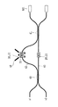
近年の通信容量の増大に伴い、波長多重分割(WDM)技術を用いた光伝送システム(WDMシステム)がバックボーンからメトロエリアの領域において広く導入されている。WDMシステムの各ノードにおいては、波長チャネル毎に光信号の光パワーをモニタすることにより、伝送信号の品質管理やシステム制御等をおこなっている。図1に、アレイ導波路回折格子型光合分波器(AWG)を用いた従来の光信号モニタについて説明する。第1のスラブ導波路12と、所定の長さずつ異なる長さを有した複数のチャネル導波路で構成されるアレイ導波路13と、第2のスラブ導波路14とで構成されているAWGに、入力導波路11と、出力導波路15が接続されており、これら導波路は、通常シリコンの基板1上において石英からなるコア2とクラッド3から構成される平面光波回路(PLC)技術によって作製することができる。AWG10は、入力導波路11から、複数の波長が合波されたWDM信号を入射すると、出力導波路15から各々の波長毎の光信号を分波して取り出すことができる(非特許文献1参照)。さらに、AWG10の各々の出力導波路15の端面に直接フォトダイオード(PD)501を実装することで、波長毎の光信号の光パワーをモニタできるコンパクトな光チャネルモニタ(OCM)が開発されている(非特許文献2参照)。ここで用いたPD501は、筐体502とガラス窓503の中で気密封止されたチップスケールパッケージ型PDアレイ(CSP型PDアレイ)500を用いた例を示している(非特許文献3参照)。CSP型PDアレイ500内に内蔵された各々PD501の受光面は、AWG10の出力導波路15の各々と光学的に結合して実装されている。
With an increase in communication capacity in recent years, an optical transmission system (WDM system) using wavelength division multiplexing (WDM) technology has been widely introduced from the backbone to the metro area. Each node of the WDM system monitors the optical power of the optical signal for each wavelength channel, thereby performing transmission signal quality management, system control, and the like. A conventional optical signal monitor using an arrayed waveguide grating optical multiplexer / demultiplexer (AWG) will be described with reference to FIG. An AWG composed of a
WDMシステムの大容量化のひとつの方法として、チャンネルの周波数間隔を狭くしていく方法がある。周波数間隔が狭くなるほど、システム上要求される波長精度が厳しくなる。そのため、WDMシステムで用いられる光信号モニタには、光パワーのみならず波長さらには光信号強度比(OSNR)を検出する機能の実装が求められている。 One method for increasing the capacity of a WDM system is to narrow the channel frequency interval. The narrower the frequency interval, the more severe the wavelength accuracy required in the system. Therefore, an optical signal monitor used in the WDM system is required to have a function for detecting not only the optical power but also the wavelength and the optical signal intensity ratio (OSNR).
しかし、先に述べた従来の技術によるAWGを用いた光信号モニタでは、分波された光信号の光パワーしか検出できないという課題があった。 However, the optical signal monitor using the AWG according to the prior art described above has a problem that only the optical power of the demultiplexed optical signal can be detected.
本発明は、従来の技術で生じていた課題に鑑みてなされたもので、その目的とするところは、光パワーの検出に加え、波長、光信号強度比(OSNR)を検出する機能を実装した光信号モニタを提供することにある。 The present invention has been made in view of the problems that have arisen in the prior art. The purpose of the present invention is to implement a function of detecting a wavelength and an optical signal intensity ratio (OSNR) in addition to the detection of optical power. It is to provide an optical signal monitor.
このような課題を解決するために、請求項1に記載の発明は、入力した波長多重光を分波して異なる波長の複数の光を出力する光信号モニタにおいて、長さの異なる複数のチャネル導波路であって、前記複数のチャネル導波路間で生じる位相差の波長による変化により前記波長多重光を分波する複数のチャネル導波路と、光の進行方向と交差するように配置され、各波長の光に対する前記位相差を温度により変化させる材料と、前記材料を加熱または冷却する機構と、出力部に配置された、1つ又は複数のフォトダイオードとを備えることを特徴とする。
In order to solve such a problem, the invention according to
また、請求項2に記載の発明は、請求項1において、所定の長さずつ異なる長さを有した前記複数のチャネル導波路で構成されるアレイ導波路回折格子と、前記アレイ導波路回折格子と入力用のチャネル導波路との間に配置された入力側のスラブ導波路と、前記アレイ導波路回折格子と複数の出力用のチャネル導波路との間に配置された出力側のスラブ導波路とを備え、前記いずれの導波路も、上部クラッド、コア、及び下部クラッドで構成されており、前記入力側または出力側のスラブ導波路は、入力した各波長の光に対して、前記入力側のスラブ導波路からの複数のチャネル導波路を経て前期出力側のスラブ導波路に至る経路間で生じる位相差を変化させる前記材料を、光の進行方向と交差するように湾曲状に形成した溝に充填して含み、前記溝は、前記入力側または出力側のスラブ導波路から前記上部クラッドおよび前記コアを除去することにより形成されるか、または前記入力側あるいは出力側のスラブ導波路から前記上部クラッド、前記コアおよび前記下部クラッドを除去することにより形成され、前記材料は、前記材料が含まれるスラブ導波路の実効屈折率の温度係数と異なる屈折率温度係数を有する材料であることを特徴とする。
The invention according to
また、請求項3に記載の発明は、請求項2において、前記溝は、前記入力側または出力側のスラブ導波路に形成された、前記材料を充填するための複数の溝であり、前記複数の溝はグループ化され、前記材料を独立に加熱または冷却する機構をグループ毎に備えることを特徴とする。
The invention according to
また、請求項4に記載の発明は、請求項1において、所定の長さずつ異なる長さを有した前記複数のチャネル導波路で構成されるアレイ導波路回折格子と、前記アレイ導波路回折格子と入力用のチャネル導波路との間に配置された入力側のスラブ導波路と、前記アレイ導波路回折格子と出力用のチャネル導波路との間に配置された出力側のスラブ導波路と
を備え、前記いずれの導波路も、上部クラッド、コア、及び下部クラッドで構成されており、前記アレイ導波路回折格子に跨って溝が形成され、前記溝は、前記チャネル導波路から前記上部クラッド及び前記コアを除去することにより形成されるか、または前記チャネル導波路から前記上部クラッド、前記コア、及び前記下部クラッドを除去することにより形成され、前記溝には、前記チャネル導波路の実効屈折率の温度係数と異なる屈折率温度係数を有する前記材料が充填されることを特徴とする。
According to a fourth aspect of the present invention, in the first aspect, the arrayed waveguide diffraction grating composed of the plurality of channel waveguides having different lengths by a predetermined length, and the arrayed waveguide diffraction grating And an input side slab waveguide disposed between the arrayed waveguide diffraction grating and the output channel waveguide, and an output slab waveguide disposed between the arrayed waveguide grating and the output channel waveguide. Each of the waveguides includes an upper clad, a core, and a lower clad, and a groove is formed across the arrayed waveguide diffraction grating, and the groove extends from the channel waveguide to the upper clad and It is formed by removing the core or by removing the upper cladding, the core, and the lower cladding from the channel waveguide, and the groove has the It said material having a temperature coefficient different from the refractive index temperature coefficient of the effective refractive index of the channel waveguide is characterized in that it is filled.
また、請求項5に記載の発明は、請求項4において、前記溝は、前記アレイ導波路回折格子を構成する前記複数のチャネル導波路に跨って形成された、前記材料を充填するための複数の溝であり、前記複数の溝はグループ化され、前記第2の材料を独立に加熱または冷却する機構をグループ毎に備えることを特徴とする。 According to a fifth aspect of the present invention, in the fourth aspect of the present invention, the groove is a plurality of grooves for filling the material formed across the plurality of channel waveguides constituting the arrayed waveguide diffraction grating. The plurality of grooves are grouped, and a mechanism for independently heating or cooling the second material is provided for each group.
また、請求項6に記載の発明は、請求項1において、前記複数のチャネル導波路は、上部クラッド、コア、及び下部クラッドで構成されており、N+1(Nは、1以上の整数)個の光カプラと隣接する光カプラとに挟まれたN組のアーム導波路であり、前記N組のアーム導波路のそれぞれは、光路長が異なる第1のアーム導波路と第2のアーム導波路で構成され、前記第1のアーム導波路または前記第2のアーム導波路の少なくとも一方に溝が形成され、前記溝は、前記溝が形成されるアーム導波路から前記上部クラッド及び前記コアを除去することにより形成されるか、または前記溝が形成されるアーム導波路から前記上部クラッド、前記コア、及び前記下部クラッドを除去することにより形成され、前記溝には、前記溝が形成されるアーム導波路の実効屈折率の温度係数と異なる屈折率温度係数を有する前記材料が充填されることを特徴とする。 According to a sixth aspect of the present invention, in the first aspect, the plurality of channel waveguides include an upper cladding, a core, and a lower cladding, and N + 1 (N is an integer equal to or greater than 1). N sets of arm waveguides sandwiched between an optical coupler and an adjacent optical coupler, and each of the N sets of arm waveguides includes a first arm waveguide and a second arm waveguide having different optical path lengths. And a groove is formed in at least one of the first arm waveguide or the second arm waveguide, and the groove removes the upper cladding and the core from the arm waveguide in which the groove is formed. Formed by removing the upper clad, the core, and the lower clad from the arm waveguide in which the groove is formed, and the arm in which the groove is formed The material having the refractive index temperature coefficient different from the temperature coefficient of the effective refractive index of the waveguide is filled.
また、請求項7に記載の発明は、請求項1において、前記複数のチャネル導波路は、上部クラッド、コア、下部クラッドで構成されており、1つ又は複数の光分岐カプラを接続して構成された、M(Mは、2以上の整数)ポートの出力を有する第1の光分岐カプラのそれぞれの出力と、1つ又は複数の光分岐カプラを接続して構成された、前記第1の光分岐カプラの出力のポート数と同数の入力のポート数を有する第2の光分岐カプラのそれぞれの入力との間に設けられた、各々が異なる遅延量を有するM本の遅延導波路であり、前記M本の遅延導波路のうちの少なくとも1つの一部に溝が形成され、前記溝は、前記溝が形成される遅延導波路から前記上部クラッド及び前記コアを除去することにより形成されるか、または前記溝が形成される遅延導波路から前記上部クラッド、前記コア、及び前記下部クラッドを除去することにより形成され、前記溝には、前記溝が形成される遅延導波路の実効屈折率の温度係数と異なる屈折率温度係数を有する前記材料が充填されていることを特徴とする。 According to a seventh aspect of the present invention, in the first aspect, the plurality of channel waveguides are configured by an upper cladding, a core, and a lower cladding, and are configured by connecting one or more optical branching couplers. Each of the first optical branching couplers having outputs of M (M is an integer of 2 or more) ports and one or a plurality of optical branching couplers connected to each other. M delay waveguides, each having a different amount of delay, are provided between each of the second optical branch couplers having the same number of input ports as the number of output ports of the optical branch coupler. A groove is formed in a part of at least one of the M delay waveguides, and the groove is formed by removing the upper cladding and the core from the delay waveguide in which the grooves are formed. Or the groove is formed A refractive index temperature coefficient different from the temperature coefficient of the effective refractive index of the delay waveguide in which the groove is formed, wherein the groove is formed by removing the upper cladding, the core, and the lower cladding from the delay waveguide. It is filled with the said material which has.
また、請求項8に記載の発明は、請求項1において、前記複数のチャネル導波路は、円状のリング導波路、及び1つ又は2つの入出力導波路であり、前記リング導波路は、上部クラッド、コア、及び下部クラッドで構成されており、前記リング導波路は、前記リング導波路から前記上部クラッド及び前記コアを除去することにより、または前記リング導波路から前記上部クラッド、前記コア、及び前記下部クラッドを除去することにより形成される溝を備え、前記溝には、前記リング導波路の実効屈折率の温度係数と異なる屈折率温度係数を有する前記材料が充填されていることを特徴とする。
The invention according to claim 8 is the invention according to
本発明によれば、光干渉回路を局所的に加熱して位相を変化させた波長可変フィルタの出力部に複数のPDを具備して、OSNRやピーク波長を測定する光信号モニタを実現することができる。 According to the present invention, it is possible to realize an optical signal monitor that measures OSNR and peak wavelength by providing a plurality of PDs at the output part of a wavelength tunable filter whose phase is changed by locally heating an optical interference circuit. Can do.
(第1の実施例)
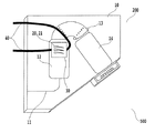
図2に、第1の実施の形態を示す。また、図3は、図2のA−A’における断面図を示す。従来と同様に石英からなる導波路で構成されるAWGにおいて、従来の実施例と異なって、第1のスラブ導波路12に楔形の溝20を形成し、その溝に光学樹脂を充填して、さらに光学樹脂21を局所的に加熱するためのヒータ30が実装されている点に特徴がある。ここで使用される光学樹脂の屈折率温度係数は、石英のそれと異なるものを用いている。具体的には、石英の屈折率温度係数+1.1×10⁻⁵[1/℃]に対して、屈折率温度係数が、−37×10-5[1/℃]のシリコーン樹脂を、光学樹脂として用いた(特許文献1参照)。
(First embodiment)
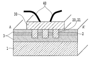
FIG. 2 shows a first embodiment. FIG. 3 is a cross-sectional view taken along the line AA ′ of FIG. In the AWG composed of a waveguide made of quartz as in the prior art, unlike the conventional example, a wedge-
また、溝20による放射損失を低減するために、溝20は通常複数に分割されて形成される。さらには、環境温度変化に伴って生じる各波長の光の等位相面の変化をキャンセルするために、スラブ導波路に形成した溝の形状は、スラブ導波路を伝搬する光の進行方向が、溝において常に光の屈折角が均一となるように溝の形状を湾曲状に配置している。
In order to reduce the radiation loss due to the
実際には、以下のとおりAWGを作製した。シリコン基板上にコアとクラッドからなる比屈折率差1.5%の石英系光導波路をPLC技術により形成した。コアのサイズは、4.5μm×4.5μmである。その後、RIEにより光学樹脂を充填する溝を加工した。溝の幅は7μmから60μmへ変化させつつ湾曲状になるように形成した。溝の数は、6分割しており、ぞの溝の間隔は40μm一定とした。溝の深さは、ここではコアよりも深い位置までクラッドをエッチングした。 Actually, an AWG was produced as follows. A quartz optical waveguide composed of a core and a clad with a relative refractive index difference of 1.5% was formed on a silicon substrate by PLC technology. The size of the core is 4.5 μm × 4.5 μm. Then, the groove | channel filled with optical resin was processed by RIE. The width of the groove was formed to be curved while changing from 7 μm to 60 μm. The number of grooves is divided into six, and the interval between the grooves is constant at 40 μm. Here, the depth of the groove was etched to a position deeper than the core.
AWG10の各々の出力導波路15の端面に直接フォトダイオード(PD)501を実装している。ここでは、CSP型PDアレイ500を用いた例を示しており、内蔵された各々PD501の受光面は、AWG10の出力導波路15の各々と光学的に結合して実装されている。
A photodiode (PD) 501 is directly mounted on the end face of each
さて、ヒータ30に電力を印加すると、光学樹脂21が局所的に加熱されてその屈折率が変化する。光学樹脂21の屈折率温度係数の絶対値は、石英による導波路のそれよりも大きいため、加熱により光学樹脂20部分での光路長が変化し、その結果AWG10の第2のスラブ導波路14の集光面において波長毎の集光位置が変化する。このことは、AWGの透過波長特性を可変にすることが可能であることを意味している。
Now, when electric power is applied to the
尚、図中示すヒータ30は、そのおおよその外形を示したものであり、実際は光学樹脂を局所的に加熱できる外付けしたヒータであればよい。さらに、ヒータ30からは電力を印加するための電気配線40が取り出されている。
In addition, the
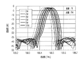
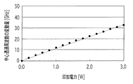
図4に、周波数間隔100GHzのAWG10に、ヒータ30としてセラミックヒータを、光学樹脂21の充填された溝20上に実装して作製したAWG201の、印加電力に対する透過波長特性を示す。印加電力に比例して、AWG201の透過波長特性がその形状に変形を伴うことなく可変であることがわかる。横軸の印加電力はすなわちピーク波長に対応付けることができるので、光学樹脂21を局所的に加熱する手段をAWG10に備えるだけで、容易にAWGの透過波長を可変にすることができる。本実施例における、印加電力に対する透過波長可変効率は、約5[GHz/W]であった。これは、ヒータ30の形状やその実装形態の最適化を行うことで、一層の改善が可能である。
FIG. 4 shows transmission wavelength characteristics with respect to applied power of an
このように、ヒータ30への印加電力に対し透過波長特性が対応するので、本AWG201のヒータ30を掃引駆動しつつ光信号光を入射し、その時出力される光パワーが最大となる印加電力を知ることによって、波長を検出することが可能となる。また、光信号が有する波長成分よりも広い範囲で、本AWG201のヒータを掃引駆動にしつつ光信号光を入射し、その時出力される光パワーの最小と最大の比を取ることにより、OSNRを検出することが可能となる。
Thus, since the transmission wavelength characteristic corresponds to the applied power to the
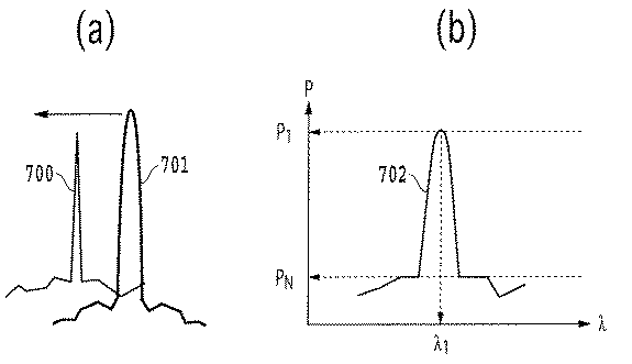
より詳細に、本構成による光信号モニタ200の動作を以下に説明する。複数の波長信号が合波されたWDM信号を、AWG10の入力導波路11より入力すると、AWGの動作原理に従い、各々の波長信号が出力導波路15毎に出力され、さらにそれぞれ波長信号毎に各PD501で受光されて電気信号に変換されて出力される。この時、ヒータ30に電力を印加すると溝20に充填された光学樹脂21が加熱されて、これまでにも述べてきたようにAWG10の透過波長特性が可動する。この時ヒータ30への印加電力は、AWG10の透過特性の可動範囲を、各隣接チャンネルの透過帯域よりも狭い範囲で掃引できる程度でよい。図5(a)に、ヒータ30を駆動しながら各チャンネルを透過してくる光信号700をモニタする様子を示す。ヒータ30に電力を印加するとそれに比例してAWG10の透過特性701が可動(図中矢印)して、それに対応するPD501からの光電流すなわちモニタ信号702が出力される(図5(b))。ヒータ30に印加する電力は、波長(λ)情報に対応付けることができるので、モニタ信号702がピークとなる印加電力すなわち波長位置(λ1)が、そのチャンネルを透過してくる光信号の波長として検出可能である。また、縦軸パワー(P)のピーク値(P1)は、光信号700の光パワーとして検出することができる。さらには、モニタ信号702のピーク値(P1)とモニタ信号のノイズレベル(PN)の値の比は、OSNRとして検出することが可能である。このように、従来の技術では光パワーしか検出できなかった光信号モニタを、本実施の形態でAWGの透過波長特性を可変化して光信号モニタを構成することにより、光パワーに加えて、波長とOSNRをモニタすることができるようになる。
In more detail, the operation of the optical signal monitor 200 according to this configuration will be described below. When a WDM signal obtained by combining a plurality of wavelength signals is input from the
ここでAWGを用いることの特徴として、透過波長特性の掃引可変域はAWGの隣接チャネル周波数間隔以下の可変域を有する程度の印加電力で駆動できる範囲であればよい。これは、AWGは出力導波路毎に、各々のチャンネル周波数(すなわち波長)の光信号を同時に出力することができるためである。よって、本実施例による光信号モニタは、各チャンネルの透過帯域よりも狭い範囲の掃引波長可変域の駆動で、波長チャンネルの全光信号を一括してモニタできるといった特徴がある。このことは、システム上の全波長域にわたって可変フィルタを掃引する方式の光信号モニタよりも、読み取り速度が高速になるといった特徴がある。 Here, as a feature of using the AWG, the sweep variable range of the transmission wavelength characteristic may be a range that can be driven with an applied power that has a variable range equal to or smaller than the adjacent channel frequency interval of the AWG. This is because the AWG can simultaneously output optical signals of respective channel frequencies (that is, wavelengths) for each output waveguide. Therefore, the optical signal monitor according to the present embodiment has a feature that all the optical signals of the wavelength channels can be collectively monitored by driving the sweep wavelength variable range narrower than the transmission band of each channel. This is characterized in that the reading speed is higher than that of an optical signal monitor that sweeps the variable filter over the entire wavelength range on the system.
なお、作製するAWG10の透過帯域幅をより狭く設計することによって、光信号の波形をより一層高精度にモニタすることが可能になる。すなわち、変調された光信号のビットレートの違いや、変調フォーマットの違いによる波形をモニタすることも可能になる。
Note that by designing the transmission bandwidth of the
以上、本発明においては、特にCSP型PDアレイ500を実装することによって、これまでにないコンパクトで環境温度に対してモニタ特性の変動がない温度無依存のOPMを構成できるという点に特徴がある。
As described above, the present invention is characterized in that, by mounting the CSP
本実施例では、ヒータ30にセラミックヒータを用いた例を示したが、局所的に加熱できる機構で実装が可能であればその種類を選ばないことは言うまでもない。例えば、ペルチェ素子、シートヒータ、抵抗発熱体等でもよい。また逆に、局所的に冷却できる機構が実装されてもよい。できれば、印加電力に対するフィルタ可変特性が最大となるような小型な加熱機構もしくは冷却機構であることが望ましい。
In the present embodiment, an example in which a ceramic heater is used as the
印加電力に対する透過波長の可変特性の効率を一層高めるためには、第1の導波路材料(本実施例では石英)中で置換され局所的に加熱もしくは冷却される第2の導波路材料(本実施例ではシリコーン樹脂)の屈折率温度係数の絶対値は、第1の導波路材料のそれよりも大きい程よい。また、第2の導波路材料を加熱もしくは冷却する場所は、第2の導波路材料の一部であってもよいし、第2の導波路材料の全体であってよい。このことは、以下に述べる各実施例においても同様に言えることである。 In order to further increase the efficiency of the variable characteristic of the transmission wavelength with respect to the applied power, a second waveguide material (this book) that is replaced in the first waveguide material (quartz in this embodiment) and locally heated or cooled. In the embodiment, the absolute value of the refractive index temperature coefficient of the silicone resin) is preferably larger than that of the first waveguide material. Further, the place where the second waveguide material is heated or cooled may be a part of the second waveguide material or the entire second waveguide material. This is also true for the embodiments described below.
また、本実施例においては、第1のスラブ導波路12に形成された溝20に充填してある光学樹脂21を局所的に加熱するためのヒータ30が実装されている例について説明したが、例えば図6に示すように、第2のスラブ導波路14に溝20を形成し、充填してある光学樹脂21を局所的に加熱するためのヒータ31を実装してもよいし、あるいは図7に示すように、アレイ導波路13の部分に溝20を形成し、充填してある光学樹脂21を局所的に加熱するためのヒータ30を実装してもよく、あるいは図8に示すように、第1のスラブ導波路14と第2のスラブ導波路の両方に溝20を形成し、充填してある光学樹脂21を局所的に加熱するためのヒータ30を実装してもよく、これらの場合についても同様の発明の効果を生むことが可能であることはいうまでもない。このことは、以下に述べる各実施例においても同様にいえることである。
In the present embodiment, the example in which the
また、ここでは、第1の導波路材料が正の屈折率温度係数を有し、第2の導波路材料が負の屈折率温度係数を有するといった、お互いが異符号の屈折率温度係数を有する組み合わせで述べたが、その他にも材料的に可能であれば、第1の導波路材料が正の屈折率温度係数を有し、第2の導波路材料も正の屈折率温度係数を有する組み合わせでも良いし、第1の導波路材料が負の屈折率温度係数を有し、第2の導波路材料も負の屈折率温度係数を有する組み合わせでも良い。すなわち、第1の導波路材料と第2の導波路材料のそれぞれの屈折率温度係数が異なればよい。印加電力に対する透過波長可変効率を最大にするために、望ましくは第2の導波路材料の屈折率温度係数の絶対値が第1の導波路材料のそれよりも大きいほどよい。このことは、以下に述べる各実施例においても同様に言えることである。 Also, here, the first waveguide material has a positive refractive index temperature coefficient, and the second waveguide material has a negative refractive index temperature coefficient. As described above in combination, the first waveguide material has a positive refractive index temperature coefficient, and the second waveguide material also has a positive refractive index temperature coefficient, if other materials are possible. Alternatively, a combination in which the first waveguide material has a negative refractive index temperature coefficient and the second waveguide material also has a negative refractive index temperature coefficient may be used. That is, it is only necessary that the refractive index temperature coefficients of the first waveguide material and the second waveguide material are different. In order to maximize the transmission wavelength variable efficiency with respect to the applied power, it is desirable that the absolute value of the refractive index temperature coefficient of the second waveguide material be larger than that of the first waveguide material. This is also true for the embodiments described below.
また、溝を埋める充填物の構成材としては、シリコーン樹脂、エポキシ樹脂、ポリメチルメタクリレート樹脂等の各種の光学樹脂、あるいはナトリウム、カリウムおよびカルシウムを含む多成分ガラス材等が使用され、一方、入出力スラブ導波路、入出力チャネル導波路、およびアレイ導波路回折格子を構成するチャネル導波路の構成材としては、多くの場合、石英系材料が使用される。 In addition, as a constituent material for filling the groove, various optical resins such as silicone resin, epoxy resin and polymethyl methacrylate resin, or multi-component glass materials containing sodium, potassium and calcium are used. In many cases, a quartz-based material is used as a constituent material of the channel waveguide constituting the output slab waveguide, the input / output channel waveguide, and the arrayed waveguide diffraction grating.
また、溝20による放射損失を低減するために、溝20は複数に分割して形成するとよい。しかし、放射損失を気にしない場合にはこの限りではない。
Further, in order to reduce the radiation loss due to the
尚、スラブ導波路に光学樹脂21を充填する溝を形成する場合には、入力導波路から出射された光において、スラブ導波路の中央付近を伝搬して光学樹脂が充填された溝を通過する際の屈折角と、スラブ導波路の中心から離れた部分を伝搬して光学樹脂が充填された溝を通過する際の屈折角とが、異なってくるために収差が生じ、その結果AWGの透過特性を劣化させる。そこで、スラブ導波路に形成した溝の形状は、スラブ導波路を伝搬する光の進行方向が、溝において常に光の屈折角が均一となるように溝の形状を湾曲状にすることで、環境温度変化に伴って生じる各波長の光の等位相面の変化をキャンセルすることができるため、最適化されたAWGの透過特性を得ることができる(特許文献2参照)。 When the groove for filling the optical resin 21 in the slab waveguide is formed, the light emitted from the input waveguide propagates near the center of the slab waveguide and passes through the groove filled with the optical resin. The refraction angle differs from the refraction angle when propagating through a portion away from the center of the slab waveguide and passing through the groove filled with the optical resin, resulting in aberration, and as a result, transmission of the AWG. Degrading properties. Therefore, the shape of the groove formed in the slab waveguide is such that the traveling direction of light propagating through the slab waveguide is curved so that the refraction angle of light is always uniform in the groove. Since it is possible to cancel the change in the equiphase plane of the light of each wavelength that occurs with the temperature change, it is possible to obtain optimized transmission characteristics of the AWG (see Patent Document 2).
また、溝の深さは、コアの下面以上にエッチングされればよい。このことは、以下に述べる各実施例においても同様に言えることである。 Further, the depth of the groove may be etched beyond the lower surface of the core. This is also true for the embodiments described below.
(第2の実施例)
図9に、第2の実施の形態を示す。また、図10は、図9のB−B’における断面図を示す。第1の実施例と異なるところは、ヒータ30として、溝21の周辺および溝21と溝21の間のクラッド3上に微細加工プロセスにより薄膜ヒータ32を集積した点である。薄膜ヒータ32にすることにより、第1の実施例でおこなった外付けヒータ30の実装工程を無くすことができるとともに、ヒータ実装による厚さ方向の増大を無くすことができるためモジュール化したとき薄型化を図ることができる。薄膜ヒータ32の材質として、例えばクロム、チタン等が挙げられるが、これらの材質だけになんら限定されるものではない。
(Second embodiment)
FIG. 9 shows a second embodiment. FIG. 10 is a cross-sectional view taken along the line BB ′ of FIG. The difference from the first embodiment is that a
実際に作製したAWGは、第1の実施例と同じである。さらに、溝と溝の間のクラッド上に集積したヒータの幅は20μmとした。 The actually produced AWG is the same as in the first embodiment. Furthermore, the width of the heater integrated on the clad between the grooves was 20 μm.
このように本実施例によれば、従来の温度無依存化したAWGにおいて、光学樹脂が充填された領域にヒータを、微細加工技術によって集積することができるため、先の第1の実施例におけるヒータの実装工程をなくすことができるようになり、透過波長可変のAWGを容易に製造することができるようになる。 As described above, according to the present embodiment, in the conventional temperature-independent AWG, the heater can be integrated in the region filled with the optical resin by the microfabrication technique. The heater mounting process can be eliminated, and an AWG having a variable transmission wavelength can be easily manufactured.
図11に、周波数間隔100GHzのAWG10に、ヒータ30として薄膜ヒータ32を集積して作製したAWGの印加電力に対する中心透過周波数特性を示す。この図から、印加電力に対する透過波長特性の可変効率は、約10[GHz/W]であることがわかる。ヒータ位置を微細加工技術により、確実に光学樹脂21が充填される溝20の直近に集積することが可能となったため、第1の実施例と比較して、印加電力に対する透過波長特性の可変効率を改善できることがわかる。
FIG. 11 shows the center transmission frequency characteristics with respect to the applied power of the AWG produced by integrating the
また、第1の実施例でも述べたように、本実施の形態を、第2のスラブ導波路14において実現してもよいし、アレイ導波路13において実現してもよい。このことは、以下に述べる各実施例においても同様に言えることである。
Further, as described in the first example, this embodiment may be realized in the
さらに、印加電力に対する透過波長特性の可変効率を改善する方策としては、溝20の分割数を多くしていき薄膜ヒータ32を集積できる領域を増やすことで、加熱領域を密に局所化することによって一層の改善を図ることができる。このことは、以下に述べる各実施例においても同様に言えることである。
Furthermore, as a measure for improving the variable efficiency of the transmission wavelength characteristic with respect to the applied power, the heating area is densely localized by increasing the number of divisions of the
また、図12に示す薄膜ヒータ32の接続パターンについて述べる。図12に溝と薄膜ヒータのパターンを抜き出して描いている。このように、図12(a)のように、薄膜ヒータ32を並列接続したパターンであってもよく、図12(b)のように、薄膜ヒータ32を直列接続したパターンであってもよく、あるいは図12(c)のように、並列接続と直列接続を取り混ぜた接続でもよく、これらになんら限定されるものではない。また、薄膜ヒータは、溝と溝の間のクラッド上に常に配置しなければならないということはなく、必要に応じて間隔をあけて配置してもよい。可能であれば、印加電力に対する透過波長特性の可変効率が最大となるようなパターンでヒータを集積することが望ましい。このことは、以下に述べる各実施例においても同様に言えることである。
A connection pattern of the
(第3の実施例)
図13に、第3の実施の形態を示す。また、図14は、図13のC−C’における断面図を示す。第2の実施例と異なるところは、薄膜ヒータ32を溝20の底部に微細加工プロセスにより集積した点である。第2の実施例における薄膜ヒータ32からの発熱は、一旦クラッド3を介して溝20に充填された光学樹脂21に伝導する。一方、本実施の形態によれば、薄膜ヒータ32上に直接光学樹脂21が接して充填されるため、薄膜ヒータ32からの発熱は直接光学樹脂21に伝導する。そのため、第2の実施例と比較して印加電力に対する透過波長特性の可変効率を高めることが可能になる。さらに、印加電力に対する透過波長特性の可変効率を改善する方策としては、溝20の分割数を多くしていき薄膜ヒータ32を集積できる溝20の数を増やすことで、加熱領域を密に局所化することによって一層の改善を図ることができる。また、可能であれば、溝20の側壁にもヒータを集積してもよい。
(Third embodiment)
FIG. 13 shows a third embodiment. FIG. 14 is a cross-sectional view taken along the line CC ′ of FIG. The difference from the second embodiment is that the
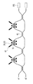
(第4の実施例)
図15に、第4の実施の形態を示す。本実施の形態では、以上述べてきた実施の形態と異なって、第1のスラブ導波路12において、光学樹脂21を充填する溝20の配置に特徴がある。すなわち、前述の実施例で形成した楔形の溝を、第1の溝部と呼ぶことにすると、その第1の溝部とは逆の向きに第2の溝部を形成し、第1の溝部および第2の溝部の周辺にも、それぞれの溝に充填した光学樹脂を加熱できるようにヒータ32が集積してある点である。第1の溝部121周辺に配置されたヒータを第1のヒータ131、第2の溝部122周辺に配置されたヒータを第2のヒータ132と呼ぶことにする。但し、第1のヒータ131と第2のヒータ132はお互い独立して電力を印加できる電気配線40、41にしておく必要がある。第2のヒータ132を配置したことにより、第2の溝部122に充填された光学樹脂21においても、加熱により屈折率を変えるため光路長が変化し、その結果AWG10の第2のスラブ導波路14の集光面において各波長の集光位置が変化する。しかし、第2の溝部122は第1の溝部121に対して逆の向きなので、第1の溝部121に充填された光学樹脂21を加熱して得られる第2のスラブ導波路14の集光面の集光方向とは逆の向きに作用する。この点を応用して、通常は第1のヒータ131を駆動して透過波長特性を可変にして使用するところを、さらに第2のヒータ132を別途駆動することにより、透過波長特性の可変速度を制御することが可能になる。すなわち、第1のヒータ131と第2のヒータ132との間で制御回路を組んで駆動することにより、波長可変フィルタの掃引速度を可変にしたり、任意の透過波長特性ポイントに高速チューニングすることが可能になる。
(Fourth embodiment)
FIG. 15 shows a fourth embodiment. In the present embodiment, unlike the embodiments described above, the
ここでは、溝20を分割した構成例を示したが、必ずしも分割する必要はないが、溝を分割することにより、放射損失を低減すること可能であり、かつヒータを局所的に密に集積することにより、透過波長特性の可変効率を高めることができる。また、第1の溝部を構成する各溝20と、第2の溝部を構成する各溝20とは、第1のヒータ131と第2のヒータ132を駆動する機構を独立して実装すれば、それぞれの溝パターンを交互にあるいは複数配置してもよい。
Here, although the configuration example in which the
また、第1の溝部121と第2の溝部122の配置(グループ化)は、他にも多様に配置することが可能である。すなわち、図15に示すように、第1の溝部121と第2の溝部122の両方を第1のスラブ導波路12に配置し、かつ第2の溝部122を入力導波路11側に配置した形態でもよいし、第1の溝部121と第2の溝部122の両方を第1のスラブ導波路12に配置し、かつ第1の溝部を入力導波路11側に配置してもよい。さらには、第1の溝部121と第2の溝部122の両方を第2のスラブ導波路14に配置し、かつ第2の溝部122を出力導波路15側に配置した形態でもよいし、第1の溝部121と第2の溝部122の両方を第2のスラブ導波路12に配置し、かつ第1の溝部を出力導波路15側に配置してもよい。さらには、第1の溝部121を第1のスラブ導波路12に配置し、第2の溝部122を第2のスラブ導波路14に配置してもよいし、逆に、第1の溝部121を第2のスラブ導波路14に配置し、第2の溝部122を第1のスラブ導波路12に配置してもよい。さらには、アレイ導波路13の部分に、第1の溝部121と第2の溝部122を配置してもよい。また、レイアウト上可能であれば、第1の溝部121を構成する溝20と第2の溝部122を構成する溝20を織り交ぜながら配置してもよい。但し、第1のヒータ131と第2のヒータ132は独立して駆動させるので、相互間の熱干渉を低減させるためには、第1の溝部121と第2の溝部122を別々に離して配置できる、第1のスラブ導波路12と第2のスラブ導波路14にそれぞれを配置した方が望ましい。
Further, the arrangement (grouping) of the first groove 121 and the second groove 122 can be variously arranged. That is, as shown in FIG. 15, both the first groove 121 and the second groove 122 are disposed in the
(第5の実施例)
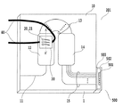
図16に、第5の実施の形態を示す。本実施例が、先の実施例と異なる点は、CSP−PDアレイが第2のスラブ14の端面に取り付けられている点である。こうすることにより、出力導波路部分を無くすことができるので、光信号モニタの小型化をいっそう進めることが可能となる。尚、ヒータは、特にこの形態に限定されるものではない。
(Fifth embodiment)
FIG. 16 shows a fifth embodiment. This embodiment is different from the previous embodiment in that the CSP-PD array is attached to the end face of the
(第6の実施例)
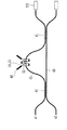
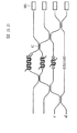
図17に第6の実施の形態を示す。これは、第1の光カプラ60と第2の光カプラ61と、これらふたつの光カプラを連結する第1のアーム導波路62と第2のアーム導波路63とで構成されるマッハツェンダ光干渉回路である。尚、本実施例では、第1および第2の光カプラを、方向性結合器で構成した例を示す。また、第1のアーム導波路の長さと第2のアーム導波路の長さは異なっており、第1のアーム導波路の長さが第2のアーム導波路の長さより長いとして以下説明する。第1の導波路材料で形成した本マッハツェンダ光干渉回路において、その第1のアーム導波路の一部に溝20を形成して、第1の導波路材料とは異なる第2の導波路材料をそこに充填する。例えば、第1の導波路材料として、屈折率温度係数α1が、+1.1×10⁻⁵[1/℃]の石英を、また、第2の導波路材料として、屈折率温度係数α2が、−37×10-5[1/℃]のシリコーン樹脂を用いる。
(Sixth embodiment)
FIG. 17 shows a sixth embodiment. This is a Mach-Zehnder optical interference circuit composed of a first
以上の構成において、溝20に充填した光学樹脂21を局所的に加熱するために薄膜ヒータ32を溝周辺に集積する。このヒータに電力を印加すると、透過波長特性が可変のマッハツェンダ光干渉回路を実現することができる。その透過特性を計算した一例を、図18に示す。すなわち、本実施例によれば、透過波長特性が可変のマッハツェンダ光干渉回路を提供することができるようになる。
In the above configuration, the
さらに、マッハツェンダ光干渉回路の出力導波路端面にPD501を取り付ける。ここで、透過波長特性をヒータ加熱により掃引すると、それに応じてPD501からの光電流すなわちモニタ信号が出力される。ここの動作は、第1の実施例で述べたとおりである。このように、透過波長特性の掃引により、光パワーのみならず波長およびOSNRも検出する光信号モニタを構成することが可能である。
Further, the
また、ヒータの集積方法としては、第1の実施例で述べたようにヒータ31を外付けで取り付けてもよいし、第2の実施例で述べたように、溝周辺のクラッド3上に薄膜ヒータ32を集積してもよいし、第3の実施例で述べたように、溝20の底部に薄膜ヒータ32を集積してもよく、その実現形態になんら制約はない。また、ヒータ等による加熱機構ではなく、冷却機構でもよいことはいうまでもない。
As a heater integration method, the heater 31 may be attached externally as described in the first embodiment, or a thin film is formed on the clad 3 around the groove as described in the second embodiment. The
またここでも、溝を分割した構成例を示したが、必ずしも分割する必要はないが、溝を分割することにより、放射損失を低減することが可能である。さらに、図19に示すように、第2のアーム導波路側にも、光学樹脂を充填する第1のアーム導波路を同じ光路長分の溝を形成し、光学樹脂を充填することにより、溝を形成したことによる両アーム導波路間の損失を均一化してもよい。 Also here, the configuration example in which the groove is divided is shown. However, although it is not always necessary to divide the groove, it is possible to reduce the radiation loss by dividing the groove. Further, as shown in FIG. 19, a groove for the same optical path length is formed in the first arm waveguide filled with the optical resin on the second arm waveguide side, and the groove is formed by filling the optical resin. The loss between both arm waveguides due to the formation of may be made uniform.
(第7の実施例)
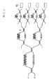
図20に第7の実施の形態を示す。これは、マッハツェンダ光干渉回路のアーム導波路をM段縦列に接続したM段ラティス光干渉回路である。さらに、M段ラティス光干渉回路は、M+1個の光カプラと、当該光カプラの隣接相互間に配置されたM個の遅延部とからなり、当該遅延部は、第1のアーム導波路と第2のアーム導波路より構成されており、第1のアーム導波路と第2のアーム導波路の長さの差はΔLに設定されている。
(Seventh embodiment)
FIG. 20 shows a seventh embodiment. This is an M-stage lattice optical interference circuit in which arm waveguides of Mach-Zehnder optical interference circuits are connected in M-stage columns. Further, the M-stage lattice optical interference circuit includes M + 1 optical couplers and M delay units disposed between adjacent ones of the optical couplers, and the delay units include the first arm waveguide and the first optical waveguide. The length difference between the first arm waveguide and the second arm waveguide is set to ΔL.
第1の導波路材料で形成した本ラティス光干渉回路において、その第1のアーム導波路の一部に溝を形成し、第1の導波路材料とは異なる第2の導波路材料をそこに充填した。ここでは、第1の導波路材料として、屈折率温度係数α1が、+1.1×10⁻⁵[1/℃]の石英を、また、第2の導波路材料として、屈折率温度係数α2が、−37×10-5[1/℃]のシリコーン樹脂を用いる。 In this lattice optical interference circuit formed of the first waveguide material, a groove is formed in a part of the first arm waveguide, and a second waveguide material different from the first waveguide material is formed therein. Filled. Here, quartz having a refractive index temperature coefficient α 1 of + 1.1 × 10 −5 [1 / ° C.] is used as the first waveguide material, and the refractive index temperature coefficient α is used as the second waveguide material. 2 uses a silicone resin of −37 × 10 −5 [1 / ° C.].
M段ラティス光干渉回路の透過スペクトルは、下記式で表される。 The transmission spectrum of the M-stage lattice optical interference circuit is expressed by the following equation.
ここで、Mは段数、xqは振幅係数、ΔLはアーム導波路間の光路長差、fは光周波数、cは光速である。(尚、M=1の時は、実施例6で述べた1段のマッハツェンダ光干渉回路に相当する。) Here, M is the number of stages, xq is the amplitude coefficient, ΔL is the optical path length difference between the arm waveguides, f is the optical frequency, and c is the speed of light. (M = 1 corresponds to the one-stage Mach-Zehnder optical interference circuit described in the sixth embodiment.)
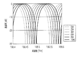
以上の構成において、溝に充填した光学樹脂を局所的に加熱するために薄膜ヒータを第1のアーム導波路に形成した溝周辺に集積する。このヒータに電力を印加することにより、透過波長特性が可変のラティス型光回路を実現した。その透過波長特性を図21に示す。すなわち、本実施例によれば、透過波長特性が可変のラティス光干渉回路を提供することができる。 In the above configuration, a thin film heater is integrated around the groove formed in the first arm waveguide in order to locally heat the optical resin filled in the groove. By applying electric power to this heater, a lattice type optical circuit with variable transmission wavelength characteristics was realized. The transmission wavelength characteristics are shown in FIG. That is, according to the present embodiment, it is possible to provide a lattice optical interference circuit having a variable transmission wavelength characteristic.
さらに、M段ラティス光干渉回路の出力導波路端面にPD501を取り付ける。ここで、透過波長特性をヒータ加熱により掃引すると、それに応じてPD501からの光電流すなわちモニタ信号が出力される。ここの動作は、第1の実施例で述べたとおりである。このように、透過波長特性の掃引により、光パワーのみならず波長およびOSNRも検出する光信号モニタを構成することが可能である。
Further, the
なお、本実施形態では、第1から第M遅延部の光路長差を全てΔLに設定したが、遅延部ごとに光路長差を変えても良い。 In this embodiment, the optical path length differences of the first to Mth delay units are all set to ΔL, but the optical path length difference may be changed for each delay unit.
またここでも、溝を分割した構成例を示したが、必ずしも分割する必要はないが、溝を分割することにより、放射損失を低減することが可能である。さらに、図22に示すように、第2のアーム導波路側にも、光学樹脂を充填する第1のアーム導波路と同じ光路長分の溝を形成し、光学樹脂を充填することにより、溝を形成したことによる両アーム導波路間の損失を均一化してもよい。 Also here, the configuration example in which the groove is divided is shown. However, although it is not always necessary to divide the groove, it is possible to reduce the radiation loss by dividing the groove. Further, as shown in FIG. 22, a groove having the same optical path length as that of the first arm waveguide filled with the optical resin is formed on the second arm waveguide side, and the groove is formed by filling the optical resin. The loss between both arm waveguides due to the formation of may be made uniform.
(第8の実施例)
図23に第8の実施の形態を示す。これは、マッハツェンダ光干渉回路のアーム導波路をM段並列に接続したM段トランスバーサル光干渉回路である。M段トランスバーサル光干渉回路は、入力をM本の導波路に分波する光カプラ(第1の光分岐カプラに対応)と、当該光カプラに接続されたM本のアーム導波路(遅延導波路に対応)と、当該M本のアーム導波路を合波する光カプラ(第2の光分岐カプラに対応)より構成されている。第1のアーム導波路に対する第2から第Mのアーム導波路の光路長差は、それぞれ、ΔL+φ2、2ΔL+φ3、・・・、(M−1)ΔL+φMに設定されている。ただし、φMは、第Mのアーム導波路の位相である。
(Eighth embodiment)
FIG. 23 shows an eighth embodiment. This is an M-stage transversal optical interference circuit in which arm waveguides of a Mach-Zehnder optical interference circuit are connected in M stages in parallel. The M-stage transversal optical interference circuit includes an optical coupler (corresponding to the first optical branching coupler) that demultiplexes an input into M waveguides, and M arm waveguides (delayed waveguides) connected to the optical coupler. And an optical coupler (corresponding to the second optical branching coupler) for multiplexing the M arm waveguides. The optical path length differences of the second to M-th arm waveguides with respect to the first arm waveguide are set to ΔL + φ 2 , 2ΔL + φ 3 ,... (M−1) ΔL + φ M , respectively. Here, φ M is the phase of the Mth arm waveguide.
第1の導波路材料で形成した本トランスバーサル光干渉回路において、その第1から第M−1のアーム導波路の一部に溝を形成し、第1の導波路材料とは異なる第2の導波路材料をそこに充填した。ここでは、第1の導波路材料として、屈折率温度係数α1が、+1.1×10⁻⁵[1/℃]の石英を、また、第2の導波路材料として、屈折率温度係数α2が、−37×10-5[1/℃]のシリコーン樹脂を用いた。 In the transversal optical interference circuit formed of the first waveguide material, a groove is formed in a part of the first to (M−1) -th arm waveguides, and the second is different from the first waveguide material. The waveguide material was filled there. Here, as the first waveguide material, the refractive index temperature coefficient alpha 1 is a quartz + 1.1 × 10 -5 [1 / ℃], also as the second waveguide material, the refractive index temperature coefficient alpha 2 used a silicone resin of −37 × 10 −5 [1 / ° C.].
M段トランスバーサル光干渉回路の透過スペクトルは、下記式で表される。 The transmission spectrum of the M-stage transversal optical interference circuit is expressed by the following equation.
![]()
![]()
ここで、Mは段数、xqは振幅係数、ΔLはアーム導波路間の光路長差、fは光周波数、cは光速である。 Here, M is the number of stages, xq is the amplitude coefficient, ΔL is the optical path length difference between the arm waveguides, f is the optical frequency, and c is the speed of light.
以上の構成において、溝に充填した光学樹脂を局所的に加熱するために薄膜ヒータを第1から第M−1のアーム導波路に形成した溝周辺に集積する。このヒータに電力を印加することにより、透過波長特性が可変のトランスバーサル光干渉回路を実現した。 In the above configuration, in order to locally heat the optical resin filled in the groove, the thin film heater is integrated around the groove formed in the first to M-1th arm waveguides. By applying power to this heater, a transversal optical interference circuit with variable transmission wavelength characteristics was realized.
さらに、M段トランスバーサル光干渉回路の出力導波路端面にPD501を取り付ける。PD501は単チャンネルのCSP型PDアレイ500を実装してもよいが、その形態は特には問わない。すなわち、前述したGSP−PDアレイでもよい。
Further, the
ここで、透過波長特性をヒータ加熱により掃引すると、それに応じてPD501からの光電流すなわちモニタ信号が出力される。ここの動作は、第1の実施例で述べたとおりである。このように、透過波長特性の掃引により、光パワーのみならず波長およびOSNRも検出する光信号モニタを構成することが可能である。
Here, when the transmission wavelength characteristic is swept by heater heating, a photocurrent, that is, a monitor signal is output from the
またここでも、溝を分割した構成例を示したが、必ずしも分割する必要はないが、溝を分割することにより、放射損失を低減することが可能である。さらに、図24に示すように、全てのアーム導波路に、同じ光路長分の溝を形成し、光学樹脂を充填することによりアーム導波路間の損失を均一化してもよい。望ましくは、損失均一化のための溝は、ヒータ集積部分から離れたところに形成するほうがよい。 Also here, the configuration example in which the groove is divided is shown. However, although it is not always necessary to divide the groove, it is possible to reduce the radiation loss by dividing the groove. Furthermore, as shown in FIG. 24, it is also possible to make the loss between the arm waveguides uniform by forming grooves for the same optical path length in all the arm waveguides and filling with optical resin. Desirably, the groove for equalizing the loss should be formed away from the heater integrated portion.
(第9の実施例)
図25に第9の実施の形態を示す。これは、1入力2出力のマッハツェンダ光干渉回路をM段、多段に接続した1×2Mフィルタである。第m段目のマッハツェンダ光干渉回路の光路長差は、2M-m・ΔL+φm,kに設定されている。ただし、φm,kは、m段目の素子のうち、k個目の素子の位相である。例えば、図24の構成では、
1段目、1個目の素子の光路長差は、4ΔL+φ1,1
2段目、1個目の素子の光路長差は、2ΔL+φ2,1
2段目、2個目の素子の光路長差は、2ΔL+φ2,2
3段目、1個目の素子の光路長差は、ΔL+φ3,1
3段目、2個目の素子の光路長差は、ΔL+φ3,2
3段目、3個目の素子の光路長差は、ΔL+φ3,3
3段目、4個目の素子の光路長差は、ΔL+φ3,4
ここで、φ1,1=0、φ2,1=π/2、φ2,2=0、φ3,1=π/4、φ3,2=3π/4、φ3,3=π/2、φ3,4=0に設定した時の、その透過波長特性を図26(a)に示す。
(Ninth embodiment)
FIG. 25 shows a ninth embodiment. This is 1 × 2 M filter connecting the Mach-
The optical path length difference between the first and first elements is 4ΔL + φ1,1
The optical path length difference between the second stage and the first element is 2ΔL + φ2,1
The optical path length difference between the second and second elements is 2ΔL + φ2,2
The optical path length difference between the third stage and the first element is ΔL + φ3,1
The optical path length difference between the third and second elements is ΔL + φ3,2
The optical path length difference between the third and third elements is ΔL + φ3,3
The optical path length difference between the third and fourth elements is ΔL + φ3,4
Here, φ1,1 = 0, φ2,1 = π / 2, φ2,2 = 0, φ3,1 = π / 4, φ3,2 = 3π / 4, φ3,3 = π / 2, φ3,4 FIG. 26A shows the transmission wavelength characteristic when = 0 is set.
第1の導波路材料で形成した本1×2Mフィルタにおいて、そのアーム導波路の一部に溝を形成し、第1の導波路材料とは異なる第2の導波路材料をそこに充填した。ここでは、第1の導波路材料として、屈折率温度係数α1が、+1.1×10⁻⁵[1/℃]の石英を、また第2の導波路材料として、屈折率温度係数α2が、−37×10-5[1/℃]のシリコーン樹脂を用いた。 In the present 1 × 2 M filter formed of the first waveguide material, a groove is formed in a part of the arm waveguide, and a second waveguide material different from the first waveguide material is filled therein. . Here, quartz having a refractive index temperature coefficient α 1 of + 1.1 × 10 −5 [1 / ° C.] is used as the first waveguide material, and the refractive index temperature coefficient α 2 is used as the second waveguide material. However, a silicone resin of −37 × 10 −5 [1 / ° C.] was used.
以上の構成において、溝に充填した光学樹脂を局所的に加熱するために薄膜ヒータを溝周辺に集積する。 In the above configuration, the thin film heater is integrated around the groove in order to locally heat the optical resin filled in the groove.
前述したように、溝に充填した光学樹脂を局所的に加熱した時の入力ポート1、出力ポート1のその透過波長特性を図26(b)に示す。このヒータに電力を印加することにより、透過波長特性が可変のマッハツェンダ光干渉回路型1×2Mフィルタを実現できる。
As described above, the transmission wavelength characteristics of the
さらに、マッハツェンダ光干渉回路型1×2Mフィルタの出力導波路端面にPD501を取り付ける。PD501は単チャンネルのCSP型PDアレイ500を実装してもよいが、その形態は特には問わない。すなわち、前述した多チャンネルのCSP−PDアレイでもよい。尚、PDを取り付ける出力ポートは、マッハツェンダ光干渉回路型1×2Mフィルタの設計に依存する。
Further, the
ここで、透過波長特性をヒータ加熱により掃引すると、それに応じてPD501からの光電流すなわちモニタ信号が出力される。ここの動作は、第1の実施例で述べたとおりである。このように、透過波長特性の掃引により、光パワーのみならず波長およびOSNRも検出する光信号モニタを構成することが可能である。
Here, when the transmission wavelength characteristic is swept by heater heating, a photocurrent, that is, a monitor signal is output from the
またここでも、溝を分割した構成例を示したが、必ずしも分割する必要はないが、溝を分割することにより、放射損失を低減することが可能である。さらに、図27に示すように、対になるアーム導波路毎に、同じ光路長分の溝を形成し、光学樹脂を充填することによりアーム導波路間の損失を均一化してもよい。 Also here, the configuration example in which the groove is divided is shown. However, although it is not always necessary to divide the groove, it is possible to reduce the radiation loss by dividing the groove. Furthermore, as shown in FIG. 27, a groove for the same optical path length may be formed for each pair of arm waveguides, and the loss between the arm waveguides may be made uniform by filling with optical resin.
尚、ここでは以上の構成において、1×2Mフィルタを構成する素子として、マッハツェンダ光干渉回路を用いたが、先に述べたラティス光干渉回路やトランスバーサル光干渉回路を用いてもよいし、後述するリング光干渉回路など、その他の光干渉回路を用いてもよいし、あるいは複数の異なる光干渉回路を用いても良い。 Here, in the configuration described above, 1 × as an element constituting of 2 M filter, was used Mach-Zehnder interferometer, it may be used Lattice beam interferometer and transversal beam interferometer as described above, Other optical interference circuits such as a ring optical interference circuit described later may be used, or a plurality of different optical interference circuits may be used.
(第10の実施例)
図28に第10の実施の形態を示す。これは、2箇所において導波路70とリング導波路71との間に方向性結合器72を有するリング共振器80である。このリング共振器80は、入力ポートS1からの入力に対して、そのリング導波路の長さに依存して、その出力ポートS2からの出力特性において、急峻な透過波長特性を示す。さらに、リング共振器80の出力ポートS2にPD501を集積している。PD501は単チャンネルのCSP型PDアレイ500を実装してもよいが、その形態は特には問わない。リング導波路71の一部に形成された溝20に充填された光学樹脂21を、局所的に加熱することにより、その共振周波数(波長)を可変にすることができる。透過波長特性をヒータ加熱により掃引すると、それに応じてPD501からの光電流すなわちモニタ信号702が出力される。透過波長特性の掃引により、光パワーのみならず波長およびOSNRも検出することが可能である。
(Tenth embodiment)
FIG. 28 shows a tenth embodiment. This is a
1 基板
2 コア
3 クラッド(上部クラッド及び下部クラッドに対応)
10 AWG (波長可変フィルタに対応)
11 入力導波路(入力用のチャネル導波路に対応)
12 第1のスラブ導波路(入力側のスラブ導波路に対応)
13 アレイ導波路
14 第2のスラブ導波路(出力側のスラブ導波路に対応)
15 出力導波路(出力用のチャネル導波路に対応)
20 溝
21 光学樹脂(材料に対応)
30 ヒータ(材料を加熱または冷却する機構に対応)
31 (外付け)ヒータ
32 薄膜ヒータ
40 電気配線
60 第1の光カプラ(方向性結合器に対応)
61 第2の光カプラ(方向性結合器に対応)
62 第1のアーム導波路
63 第2のアーム導波路
70 入出力導波路
71 リング導波路
72 方向性結合器
80 リング共振器
121 第1の溝部
122 第2の溝部
131 第1のヒータ
132 第2のヒータ
200 光信号モニタ
201 AWG(波長可変フィルタに対応)
500 CSP型PDアレイ
501 PD(フォトダイオードに対応)
502 筐体
503 ガラス窓
700 光信号
701 AWGの透過特性
702 モニタ信号
1
10 AWG (compatible with wavelength tunable filter)
11 Input waveguide (corresponding to input channel waveguide)
12 First slab waveguide (corresponding to slab waveguide on the input side)
13
15 Output waveguide (corresponding to output channel waveguide)
20 groove 21 optical resin (corresponds to material)
30 Heater (corresponding to the mechanism for heating or cooling the material)
31 (External)
61 Second optical coupler (corresponding to directional coupler)
62
500 CSP
502
Claims (8)
長さの異なる複数のチャネル導波路であって、前記複数のチャネル導波路間で生じる位相差の波長による変化により前記波長多重光を分波する複数のチャネル導波路と、
光の進行方向と交差するように配置され、各波長の光に対する前記位相差を温度により変化させる材料と、
前記材料を加熱または冷却する機構と、
出力部に配置された、1つ又は複数のフォトダイオードと
を備えることを特徴とする光信号モニタ。 In an optical signal monitor that demultiplexes input wavelength multiplexed light and outputs a plurality of lights of different wavelengths,
A plurality of channel waveguides having different lengths, and a plurality of channel waveguides for demultiplexing the wavelength-multiplexed light by a change in wavelength of a phase difference generated between the plurality of channel waveguides;
A material that is arranged so as to intersect the traveling direction of light, and that changes the phase difference with respect to light of each wavelength according to temperature;
A mechanism for heating or cooling the material;
An optical signal monitor comprising one or a plurality of photodiodes arranged in an output unit.
前記アレイ導波路回折格子と入力用のチャネル導波路との間に配置された入力側のスラブ導波路と、
前記アレイ導波路回折格子と複数の出力用のチャネル導波路との間に配置された出力側のスラブ導波路と
を備え、
前記いずれの導波路も、上部クラッド、コア、及び下部クラッドで構成されており、
前記入力側または出力側のスラブ導波路は、入力した各波長の光に対して、前記入力側のスラブ導波路からの複数のチャネル導波路を経て前期出力側のスラブ導波路に至る経路間で生じる位相差を変化させる前記材料を、光の進行方向と交差するように湾曲状に形成した溝に充填して含み、
前記溝は、前記入力側または出力側のスラブ導波路から前記上部クラッドおよび前記コアを除去することにより形成されるか、または前記入力側あるいは出力側のスラブ導波路から前記上部クラッド、前記コアおよび前記下部クラッドを除去することにより形成され、
前記材料は、前記材料が含まれるスラブ導波路の実効屈折率の温度係数と異なる屈折率温度係数を有する材料であることを特徴とする請求項1に記載の光信号モニタ。 An arrayed waveguide grating composed of the plurality of channel waveguides having different lengths by a predetermined length;
A slab waveguide on the input side disposed between the arrayed waveguide grating and the input channel waveguide;
An output-side slab waveguide disposed between the arrayed waveguide grating and a plurality of output channel waveguides;
Each of the waveguides is composed of an upper clad, a core, and a lower clad,
The slab waveguide on the input side or the output side is between the paths from the input slab waveguide to the output slab waveguide through a plurality of channel waveguides for each wavelength of light input The material for changing the generated phase difference is filled in a groove formed in a curved shape so as to intersect the traveling direction of light,
The groove is formed by removing the upper cladding and the core from the input-side or output-side slab waveguide, or from the input-side or output-side slab waveguide, the upper cladding, the core, and the core Formed by removing the lower cladding,
The optical signal monitor according to claim 1, wherein the material is a material having a refractive index temperature coefficient different from a temperature coefficient of an effective refractive index of a slab waveguide including the material.
前記複数の溝はグループ化され、
前記材料を独立に加熱または冷却する機構をグループ毎に備えることを特徴とする請求項2に記載の光信号モニタ。 The grooves are a plurality of grooves formed in the input-side or output-side slab waveguide for filling the material,
The plurality of grooves are grouped;
The optical signal monitor according to claim 2, further comprising a mechanism for heating or cooling the material independently for each group.
前記アレイ導波路回折格子と入力用のチャネル導波路との間に配置された入力側のスラブ導波路と、
前記アレイ導波路回折格子と出力用のチャネル導波路との間に配置された出力側のスラブ導波路と
を備え、
前記いずれの導波路も、上部クラッド、コア、及び下部クラッドで構成されており、
前記アレイ導波路回折格子に跨って溝が形成され、
前記溝は、前記チャネル導波路から前記上部クラッド及び前記コアを除去することにより形成されるか、または前記チャネル導波路から前記上部クラッド、前記コア、及び前記下部クラッドを除去することにより形成され、
前記溝には、前記チャネル導波路の実効屈折率の温度係数と異なる屈折率温度係数を有する前記材料が充填されることを特徴とする請求項1に記載の光信号モニタ。 An arrayed waveguide grating composed of the plurality of channel waveguides having different lengths by a predetermined length;
A slab waveguide on the input side disposed between the arrayed waveguide grating and the input channel waveguide;
An output-side slab waveguide disposed between the arrayed-waveguide diffraction grating and the output channel waveguide;
Each of the waveguides is composed of an upper clad, a core, and a lower clad,
A groove is formed across the arrayed waveguide grating,
The groove is formed by removing the upper cladding and the core from the channel waveguide, or formed by removing the upper cladding, the core, and the lower cladding from the channel waveguide,
The optical signal monitor according to claim 1, wherein the groove is filled with the material having a refractive index temperature coefficient different from a temperature coefficient of an effective refractive index of the channel waveguide.
前記複数の溝はグループ化され、
前記第2の材料を独立に加熱または冷却する機構をグループ毎に備えることを特徴とする請求項4に記載の光信号モニタ。 The groove is a plurality of grooves for filling the material formed across the plurality of channel waveguides constituting the arrayed waveguide diffraction grating,
The plurality of grooves are grouped;
The optical signal monitor according to claim 4, wherein a mechanism for independently heating or cooling the second material is provided for each group.
上部クラッド、コア、及び下部クラッドで構成されており、
N+1(Nは、1以上の整数)個の光カプラと隣接する光カプラとに挟まれたN組のアーム導波路であり、
前記N組のアーム導波路のそれぞれは、光路長が異なる第1のアーム導波路と第2のアーム導波路で構成され、
前記第1のアーム導波路または前記第2のアーム導波路の少なくとも一方に溝が形成され、
前記溝は、前記溝が形成されるアーム導波路から前記上部クラッド及び前記コアを除去することにより形成されるか、または前記溝が形成されるアーム導波路から前記上部クラッド、前記コア、及び前記下部クラッドを除去することにより形成され、
前記溝には、前記溝が形成されるアーム導波路の実効屈折率の温度係数と異なる屈折率温度係数を有する前記材料が充填されることを特徴とする請求項1に記載の光信号モニタ。 The plurality of channel waveguides are:
It consists of an upper cladding, a core, and a lower cladding,
N sets of arm waveguides sandwiched between N + 1 (N is an integer of 1 or more) optical couplers and an adjacent optical coupler,
Each of the N sets of arm waveguides includes a first arm waveguide and a second arm waveguide having different optical path lengths,
A groove is formed in at least one of the first arm waveguide or the second arm waveguide;
The groove is formed by removing the upper clad and the core from an arm waveguide in which the groove is formed, or the upper clad, the core, and the core from an arm waveguide in which the groove is formed. Formed by removing the lower cladding,
The optical signal monitor according to claim 1, wherein the groove is filled with the material having a refractive index temperature coefficient different from a temperature coefficient of an effective refractive index of an arm waveguide in which the groove is formed.
上部クラッド、コア、下部クラッドで構成されており、
1つ又は複数の光分岐カプラを接続して構成された、M(Mは、2以上の整数)ポートの出力を有する第1の光分岐カプラのそれぞれの出力と、1つ又は複数の光分岐カプラを接続して構成された、前記第1の光分岐カプラの出力のポート数と同数の入力のポート数を有する第2の光分岐カプラのそれぞれの入力との間に設けられた、各々が異なる遅延量を有するM本の遅延導波路であり、
前記M本の遅延導波路のうちの少なくとも1つの一部に溝が形成され、
前記溝は、前記溝が形成される遅延導波路から前記上部クラッド及び前記コアを除去することにより形成されるか、または前記溝が形成される遅延導波路から前記上部クラッド、前記コア、及び前記下部クラッドを除去することにより形成され、
前記溝には、前記溝が形成される遅延導波路の実効屈折率の温度係数と異なる屈折率温度係数を有する前記材料が充填されていることを特徴とする請求項1に記載の光信号モニタ。 The plurality of channel waveguides are:
It consists of an upper cladding, a core, and a lower cladding,
Each output of the first optical branching coupler configured by connecting one or more optical branching couplers and having an output of M (M is an integer of 2 or more) ports, and one or more optical branching Each of which is provided between each input of a second optical branching coupler having a number of input ports equal to the number of ports of the first optical branching coupler configured by connecting the couplers. M delay waveguides having different delay amounts,
A groove is formed in a part of at least one of the M delay waveguides;
The groove is formed by removing the upper cladding and the core from the delay waveguide in which the groove is formed, or the upper cladding, the core, and the core from the delay waveguide in which the groove is formed. Formed by removing the lower cladding,
The optical signal monitor according to claim 1, wherein the groove is filled with the material having a refractive index temperature coefficient different from a temperature coefficient of an effective refractive index of the delay waveguide in which the groove is formed. .
前記リング導波路は、上部クラッド、コア、及び下部クラッドで構成されており、
前記リング導波路は、前記リング導波路から前記上部クラッド及び前記コアを除去することにより、または前記リング導波路から前記上部クラッド、前記コア、及び前記下部クラッドを除去することにより形成される溝を備え、
前記溝には、前記リング導波路の実効屈折率の温度係数と異なる屈折率温度係数を有する前記材料が充填されていることを特徴とする請求項1に記載の光信号モニタ。 The plurality of channel waveguides are a circular ring waveguide and one or two input / output waveguides,
The ring waveguide is composed of an upper clad, a core, and a lower clad,
The ring waveguide has a groove formed by removing the upper clad and the core from the ring waveguide, or by removing the upper clad, the core, and the lower clad from the ring waveguide. Prepared,
2. The optical signal monitor according to claim 1, wherein the groove is filled with the material having a refractive index temperature coefficient different from a temperature coefficient of an effective refractive index of the ring waveguide.
Priority Applications (1)
| Application Number | Priority Date | Filing Date | Title |
|---|---|---|---|
| JP2008217268A JP5086207B2 (en) | 2008-08-26 | 2008-08-26 | Optical signal monitor |
Applications Claiming Priority (1)
| Application Number | Priority Date | Filing Date | Title |
|---|---|---|---|
| JP2008217268A JP5086207B2 (en) | 2008-08-26 | 2008-08-26 | Optical signal monitor |
Publications (2)
| Publication Number | Publication Date |
|---|---|
| JP2010054620A true JP2010054620A (en) | 2010-03-11 |
| JP5086207B2 JP5086207B2 (en) | 2012-11-28 |
Family
ID=42070647
Family Applications (1)
| Application Number | Title | Priority Date | Filing Date |
|---|---|---|---|
| JP2008217268A Expired - Fee Related JP5086207B2 (en) | 2008-08-26 | 2008-08-26 | Optical signal monitor |
Country Status (1)
| Country | Link |
|---|---|
| JP (1) | JP5086207B2 (en) |
Cited By (5)
| Publication number | Priority date | Publication date | Assignee | Title |
|---|---|---|---|---|
| WO2019172158A1 (en) * | 2018-03-07 | 2019-09-12 | 日本電信電話株式会社 | Variable wavelength filter |
| US10439729B2 (en) | 2017-09-27 | 2019-10-08 | Fujitsu Limited | Optical device and optical apparatus |
| JP2020519973A (en) * | 2017-08-14 | 2020-07-02 | 河南仕佳光子科技股▲分▼有限公司 | Tunable broad-spectrum wavelength-insensitive directional coupler |
| US11119273B2 (en) | 2017-02-08 | 2021-09-14 | Rockley Photonics Limited | T-shaped arrayed waveguide grating |
| US11733461B2 (en) | 2017-07-17 | 2023-08-22 | Rockley Photonics Limited | Athermalized multi-path interference filter |
Citations (8)
| Publication number | Priority date | Publication date | Assignee | Title |
|---|---|---|---|---|
| JPS6476012A (en) * | 1987-09-18 | 1989-03-22 | Nippon Telegraph & Telephone | Periodic type optical filter |
| JPH08251105A (en) * | 1994-09-26 | 1996-09-27 | Nippon Telegr & Teleph Corp <Ntt> | Wavelength monitor device |
| JP2001116937A (en) * | 1999-10-21 | 2001-04-27 | Hitachi Cable Ltd | Optical wavelength multiplexer/demultiplexer |
| JP2002207135A (en) * | 2001-01-09 | 2002-07-26 | Nippon Telegr & Teleph Corp <Ntt> | Optical wavelength multiplexer/demultiplexer circuit |
| JP2003149478A (en) * | 1997-02-14 | 2003-05-21 | Nippon Telegr & Teleph Corp <Ntt> | Optical waveguide circuit, optical waveguide module having the optical waveguide circuit and method for manufacturing optical waveguide circuit |
| JP2004029583A (en) * | 2002-06-27 | 2004-01-29 | Nippon Telegr & Teleph Corp <Ntt> | Optical multiplexer/demultiplexer |
| JP2005242214A (en) * | 2004-02-27 | 2005-09-08 | Keio Gijuku | Optical function waveguide, optical modulator, array waveguide diffraction grating, and dispersion compensating circuit |
| JP2007271704A (en) * | 2006-03-30 | 2007-10-18 | Nec Corp | Variable light control device and variable light control method |
-
2008
- 2008-08-26 JP JP2008217268A patent/JP5086207B2/en not_active Expired - Fee Related
Patent Citations (8)
| Publication number | Priority date | Publication date | Assignee | Title |
|---|---|---|---|---|
| JPS6476012A (en) * | 1987-09-18 | 1989-03-22 | Nippon Telegraph & Telephone | Periodic type optical filter |
| JPH08251105A (en) * | 1994-09-26 | 1996-09-27 | Nippon Telegr & Teleph Corp <Ntt> | Wavelength monitor device |
| JP2003149478A (en) * | 1997-02-14 | 2003-05-21 | Nippon Telegr & Teleph Corp <Ntt> | Optical waveguide circuit, optical waveguide module having the optical waveguide circuit and method for manufacturing optical waveguide circuit |
| JP2001116937A (en) * | 1999-10-21 | 2001-04-27 | Hitachi Cable Ltd | Optical wavelength multiplexer/demultiplexer |
| JP2002207135A (en) * | 2001-01-09 | 2002-07-26 | Nippon Telegr & Teleph Corp <Ntt> | Optical wavelength multiplexer/demultiplexer circuit |
| JP2004029583A (en) * | 2002-06-27 | 2004-01-29 | Nippon Telegr & Teleph Corp <Ntt> | Optical multiplexer/demultiplexer |
| JP2005242214A (en) * | 2004-02-27 | 2005-09-08 | Keio Gijuku | Optical function waveguide, optical modulator, array waveguide diffraction grating, and dispersion compensating circuit |
| JP2007271704A (en) * | 2006-03-30 | 2007-10-18 | Nec Corp | Variable light control device and variable light control method |
Cited By (6)
| Publication number | Priority date | Publication date | Assignee | Title |
|---|---|---|---|---|
| US11119273B2 (en) | 2017-02-08 | 2021-09-14 | Rockley Photonics Limited | T-shaped arrayed waveguide grating |
| US11733461B2 (en) | 2017-07-17 | 2023-08-22 | Rockley Photonics Limited | Athermalized multi-path interference filter |
| JP2020519973A (en) * | 2017-08-14 | 2020-07-02 | 河南仕佳光子科技股▲分▼有限公司 | Tunable broad-spectrum wavelength-insensitive directional coupler |
| US10439729B2 (en) | 2017-09-27 | 2019-10-08 | Fujitsu Limited | Optical device and optical apparatus |
| WO2019172158A1 (en) * | 2018-03-07 | 2019-09-12 | 日本電信電話株式会社 | Variable wavelength filter |
| US11112561B2 (en) | 2018-03-07 | 2021-09-07 | Nippon Telegraph And Telephone Corporation | Variable wavelength filter |
Also Published As
| Publication number | Publication date |
|---|---|
| JP5086207B2 (en) | 2012-11-28 |
Similar Documents
| Publication | Publication Date | Title |
|---|---|---|
| US8369666B2 (en) | Optical wavelength multiplexing/ de-multiplexing circuit | |
| CN105700071B (en) | Temperature-insensitive DEMUX/MUX device and preparation method thereof | |
| JP2004239991A (en) | Optical functional device | |
| JP2000241656A (en) | Multiple wavelength multi-sepatation device | |
| JP4748524B2 (en) | Arrayed waveguide grating type multiplexer / demultiplexer | |
| JP5086207B2 (en) | Optical signal monitor | |
| US6993217B2 (en) | Optical switch device | |
| JP5086208B2 (en) | Tunable filter and optical signal monitor using the same | |
| KR20010078349A (en) | Wavelength multiplexing/demultiplexing unit, wavelength multiplexing/demultiplexing apparatus and wavelength multiplexing/demultiplexing method | |
| JP6509626B2 (en) | Wavelength multiplexing / demultiplexing device, optical receiver and optical transmitter | |
| JP5180118B2 (en) | Optical wavelength division multiplexing signal monitoring device | |
| JP7023317B2 (en) | Optical wavelength filter and wavelength separation optical circuit | |
| JP2010175645A (en) | Optical wavelength-multiplexed signal monitoring device and method | |
| JP7079391B2 (en) | Optical transmission equipment and optical elements | |
| KR20210023511A (en) | Wavelength demultiplexer with arrayed waveguide grating and methods of manufacturing | |
| JP4313644B2 (en) | Arrayed waveguide type wavelength multiplexer / demultiplexer and optical wavelength division multiplexing transmission apparatus | |
| JP3788397B2 (en) | Optical waveguide device and communication device using optical waveguide device | |
| JP5053980B2 (en) | Optical wavelength division multiplexing signal monitoring apparatus and method | |
| JP6251206B2 (en) | Optical transmission / reception system | |
| JP7070738B1 (en) | Optical wavelength filter | |
| JP7408032B2 (en) | Optical transmitter and optical transceiver | |
| Biswas et al. | A Review on Arrayed Waveguide Grating Multiplexer/De-multiplexer forDense Wavelength Division Multiplexing Systems | |
| KR100416983B1 (en) | Alignment element for planar lightguide circuit module | |
| US20220385373A1 (en) | Wavelength converter, optical communication apparatus, and optical waveguide substrate | |
| JP6771600B2 (en) | Optical waveguide circuit |
Legal Events
| Date | Code | Title | Description |
|---|---|---|---|
| RD02 | Notification of acceptance of power of attorney |
Free format text: JAPANESE INTERMEDIATE CODE: A7422 Effective date: 20100525 |
|
| RD04 | Notification of resignation of power of attorney |
Free format text: JAPANESE INTERMEDIATE CODE: A7424 Effective date: 20100525 |
|
| A621 | Written request for application examination |
Free format text: JAPANESE INTERMEDIATE CODE: A621 Effective date: 20100716 |
|
| RD02 | Notification of acceptance of power of attorney |
Free format text: JAPANESE INTERMEDIATE CODE: A7422 Effective date: 20100914 |
|
| A977 | Report on retrieval |
Free format text: JAPANESE INTERMEDIATE CODE: A971007 Effective date: 20120118 |
|
| A131 | Notification of reasons for refusal |
Free format text: JAPANESE INTERMEDIATE CODE: A131 Effective date: 20120120 |
|
| A521 | Written amendment |
Free format text: JAPANESE INTERMEDIATE CODE: A523 Effective date: 20120321 |
|
| TRDD | Decision of grant or rejection written | ||
| A01 | Written decision to grant a patent or to grant a registration (utility model) |
Free format text: JAPANESE INTERMEDIATE CODE: A01 Effective date: 20120904 |
|
| A01 | Written decision to grant a patent or to grant a registration (utility model) |
Free format text: JAPANESE INTERMEDIATE CODE: A01 |
|
| A61 | First payment of annual fees (during grant procedure) |
Free format text: JAPANESE INTERMEDIATE CODE: A61 Effective date: 20120906 |
|
| R150 | Certificate of patent or registration of utility model |
Ref document number: 5086207 Country of ref document: JP Free format text: JAPANESE INTERMEDIATE CODE: R150 Free format text: JAPANESE INTERMEDIATE CODE: R150 |
|
| FPAY | Renewal fee payment (event date is renewal date of database) |
Free format text: PAYMENT UNTIL: 20150914 Year of fee payment: 3 |
|
| S531 | Written request for registration of change of domicile |
Free format text: JAPANESE INTERMEDIATE CODE: R313531 |
|
| R350 | Written notification of registration of transfer |
Free format text: JAPANESE INTERMEDIATE CODE: R350 |
|
| LAPS | Cancellation because of no payment of annual fees |