JP2010041470A - Transmitter and transmission/reception device - Google Patents
Transmitter and transmission/reception device Download PDFInfo
- Publication number
- JP2010041470A JP2010041470A JP2008202851A JP2008202851A JP2010041470A JP 2010041470 A JP2010041470 A JP 2010041470A JP 2008202851 A JP2008202851 A JP 2008202851A JP 2008202851 A JP2008202851 A JP 2008202851A JP 2010041470 A JP2010041470 A JP 2010041470A
- Authority
- JP
- Japan
- Prior art keywords
- distortion compensation
- circuit
- signal
- transmission
- circuits
- Prior art date
- Legal status (The legal status is an assumption and is not a legal conclusion. Google has not performed a legal analysis and makes no representation as to the accuracy of the status listed.)
- Granted
Links
Images


Landscapes
- Transmitters (AREA)
- Amplifiers (AREA)
Abstract
Description
本発明は、複数の送信系統を有する送信機及び送受信装置であって、歪補償機能を備えた送信機及び送受信装置に関するものである。 The present invention relates to a transmitter and a transmitter / receiver having a plurality of transmission systems, and to a transmitter and a transmitter / receiver having a distortion compensation function.
近年の移動体通信システムでは通信/伝送/トラフィックデータ容量の増加等に伴い、送受信機の高性能化が求められている。また高速データ通信を実現する一手段として複数のアンテナ、送受信回路を用いたMIMO(Multiple−Input Multiple−Output)伝送技術の適用が求められている。加えて、送信系においては低消費電力・低歪化が必要であるためプリディストーション方式の歪補償を用いた電力増幅器が適用されている。 In recent mobile communication systems, as the communication / transmission / traffic data capacity increases, etc., higher performance of the transceiver is required. Further, as one means for realizing high-speed data communication, application of a MIMO (Multiple-Input Multiple-Output) transmission technique using a plurality of antennas and transmission / reception circuits is required. In addition, since it is necessary to reduce power consumption and distortion in a transmission system, a power amplifier using predistortion type distortion compensation is applied.
従来の送信機においては、適応プリディストーション方式が採用され、歪補償係数を乗算して隣接チャネル漏洩電力を抑圧している。電力増幅器で増幅した無線送信信号の一部をフィードバックし、その帰還信号を中間周波数に周波数変換する。変換した中間周波数の信号をA/D変換器でサンプリング処理することでデジタル信号に変換し、変換したデジタル信号を直交復調部でIチャネル、Qチャネルのデジタルベースバンド信号に変換する。フィードバックしたIチャネル、Qチャネルのデジタルベースバンド信号と送信信号(参照信号)のIチャネル、Qチャネルのベースバンド信号とを比較して誤差成分を算出する。この誤差成分に基づき歪補償係数を作成し、適宜、歪補償係数を更新することで低歪特性を実現している(例えば、特許文献1参照)。 In a conventional transmitter, an adaptive predistortion method is employed, and adjacent channel leakage power is suppressed by multiplying by a distortion compensation coefficient. A part of the radio transmission signal amplified by the power amplifier is fed back, and the feedback signal is frequency-converted to an intermediate frequency. The converted intermediate frequency signal is sampled by an A / D converter to be converted into a digital signal, and the converted digital signal is converted into an I channel and Q channel digital baseband signal by an orthogonal demodulator. The feedback I-channel and Q-channel digital baseband signals are compared with the I-channel and Q-channel baseband signals of the transmission signal (reference signal) to calculate an error component. A low distortion characteristic is realized by creating a distortion compensation coefficient based on this error component and updating the distortion compensation coefficient as appropriate (see, for example, Patent Document 1).
しかし、従来の送信機では、帰還信号を処理し、もとの送信信号(参照信号)と比較することで歪補償係数を生成する信号処理回路が、マルチポート増幅器のそれぞれのポート用に複数構成されている。このため、ポート数の増加に比例して回路規模・部品点数が増加し、装置の大型化や消費電力の増加という問題点があった。 However, in the conventional transmitter, a plurality of signal processing circuits that process the feedback signal and generate a distortion compensation coefficient by comparing with the original transmission signal (reference signal) are configured for each port of the multi-port amplifier. Has been. For this reason, the circuit scale and the number of parts increased in proportion to the increase in the number of ports, and there was a problem that the apparatus was enlarged and the power consumption was increased.
本発明の目的は、上述の問題を解決し、複数の電力増幅器を備えた送信機において歪補償処理を行う場合に、回路規模・部品点数を削減し、装置の小型化・低消費電力化を実現することにある。 An object of the present invention is to solve the above-described problems and reduce the circuit scale and the number of parts, and reduce the size and power consumption of the apparatus when performing distortion compensation processing in a transmitter having a plurality of power amplifiers. It is to be realized.
本発明による送信機は、帰還信号と対応する参照信号とを送信系統毎に時分割に切り替えて歪補償係数を算出し、複数の歪補償処理回路に対して時分割に歪補償係数を出力する。 The transmitter according to the present invention calculates the distortion compensation coefficient by switching the feedback signal and the corresponding reference signal to time division for each transmission system, and outputs the distortion compensation coefficient to the plurality of distortion compensation processing circuits in time division. .
本発明による送信機は、複数の電力増幅器に対する歪補償処理において、電力増幅器で増幅された無線送信信号をフィードバック処理する回路と歪補償係数を算出する回路とをそれぞれ、複数の系統において共通利用できるため、回路規模、部品点数を削減できる。このため、装置の小型化・低消費電力化・低価格化が実現できる。 The transmitter according to the present invention can commonly use a circuit for feedback processing of a radio transmission signal amplified by a power amplifier and a circuit for calculating a distortion compensation coefficient in a plurality of systems in distortion compensation processing for a plurality of power amplifiers. Therefore, the circuit scale and the number of parts can be reduced. For this reason, downsizing, low power consumption, and low price of the apparatus can be realized.
実施の形態1.
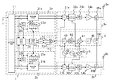
本発明の実施の形態1について図面を参照して説明する。なお、以下の各実施の形態を説明するための各図において、同一符号は、同一または相当の構成を示す。図1は本発明の実施の形態1における送信機を示すブロック構成図である。本実施の形態1における送信機は、例えば、無線通信システムの基地局の送信機として使用され、無線送信周波数と無線受信周波数とが異なるFDD(周波数分割方式)システム等に使用される。
まず、送信機の全体構成について説明する。実施の形態1の送信機は、歪補償処理回路2a、2bを有するデジタル信号処理回路1と、送信回路3a、3bと、帰還回路4と、信号生成回路6とを備えている。デジタル信号処理回路1は、例えば、FPGA等によって実現される。
First, the overall configuration of the transmitter will be described. The transmitter according to the first embodiment includes a digital
送信回路3a、3bはデジタル信号処理回路1から出力されるIチャネル、Qチャネルの補正デジタルベースバンド信号をもとに、アンテナ8a、8bそれぞれに無線送信信号を供給する。また、送信回路3a、3bは電力増幅した無線送信信号の一部を抽出し、帰還信号として帰還回路4に供給する。
The
帰還回路4は、送信回路3a、3bそれぞれから供給された帰還信号のうち、どちらか一方の信号を選択して、デジタル帰還信号を生成し、デジタル信号処理回路1に供給する。信号生成回路6は送信回路3a、3b及び帰還回路4に共通に配置され、それぞれの回路に必要な信号を供給する。
The feedback circuit 4 selects one of the feedback signals supplied from the
本実施の形態1の送信機は、2系統の送信ブロックを有しており、歪補償処理回路2a及び送信回路3aを1系とし、歪補償処理回路2b及び送信回路3bを2系とする。
The transmitter according to the first embodiment has two transmission blocks, and the distortion
次に、送信機の詳細な構成について説明する。デジタル信号処理回路1は、ベースバンド信号処理回路11と歪補償処理回路2a、2bと歪補償係数算出回路7とを有する。ベースバンド信号処理回路11は、入力された送信データからIチャネル、Qチャネルのデジタルベースバンド信号を生成し、歪補償処理回路2a、2bそれぞれに信号を供給する。
Next, a detailed configuration of the transmitter will be described. The digital
通信システムの構成により、ベースバンド信号処理回路11は、歪補償処理回路2a、2bそれぞれに同一なデジタルベースバンド信号を供給する場合と、歪補償処理回路2a、2bそれぞれに異なるデジタルベースバンド信号を供給する場合がある。本実施の形態1においては、ベースバンド信号処理回路11が異なるデジタルベースバンド信号を供給する場合を例にしている。図1において、ベースバンド信号処理回路11は、歪補償処理回路2aに対してはデジタルベースバンド信号I1、Q1を供給し、歪補償処理回路2bに対してはデジタルベースバンド信号I2、Q2を供給している。
Depending on the configuration of the communication system, the baseband
歪補償処理回路2aは、複素演算処理回路21aと、電力計算回路22aと、歪補償テーブル23aとを有する。歪補償処理回路2aは、ベースバンド信号処理回路11から供給されたデジタルベースバンド信号I1、Q1を歪補償係数算出回路7に供給する。併せて、歪補償処理回路2aは、電力計算回路22aで算出した送信信号レベル情報を歪補償係数算出回路7に供給する。
The distortion
また、歪補償処理回路2aは、電力計算回路22aで算出した送信信号レベル情報に基づき、歪補償テーブル23aに格納されている歪補償係数とデジタルベースバンド信号I1、Q1とを複素演算処理回路21aで複素演算して、補正デジタルベースバンド信号を生成する。この補正デジタルベースバンド信号を送信回路3aに供給することで、送信回路3aの主に電力増幅器34aで発生する歪を抑圧する。
Further, the distortion
ここで用いる歪補償テーブル23aは、複数の補償テーブルを保存できる構成である。歪補償係数算出回路7から出力される歪補償係数により、歪補償テーブル23aは更新される。また、歪補償テーブル23a内の複数の補償テーブルから、更新する補償テーブルを適宜切り替えることで、主に送信回路3aで発生する温度変化、経年変化に対しても安定した歪補償動作が可能となる構成となっている。
The distortion compensation table 23a used here is configured to store a plurality of compensation tables. The distortion compensation table 23 a is updated with the distortion compensation coefficient output from the distortion compensation
歪補償処理回路2bは、歪補償処理回路2aと同様の処理回路を有しており、ベースバンド信号処理回路11から供給されたデジタルベースバンド信号I2、Q2と送信信号レベル情報とを歪補償係数算出回路7に供給する。また、歪補償処理回路2aと同様の処理をして、歪補償処理回路2bは、補正デジタルベースバンド信号を送信回路3bに供給する。歪補償テーブル23bの動作についても歪補償テーブル23aと同様である。
The distortion
送信回路3aでは、歪補償処理回路2aから出力されたIチャネル、Qチャネルの補正デジタルベースバンド信号をD/A変換器31aでIチャネル、Qチャネルのアナログベースバンド信号に変換する。D/A変換器31aは、局部信号発生器62から供給されるサンプリング信号(周波数:Fs)に基づいて、入力信号を補間処理する。
In the
D/A変換器31aから出力されたIチャネル、Qチャネルのアナログベースバンド信号は、アナログ直交変調器32aに入力される。アナログ直交変調器32aは、可変信号発生器63から供給される搬送波(LO)に基づいて、Iチャネル、Qチャネルのアナログベースバンド信号を直交変調し、無線周波数に周波数変換(アップコンバージョン)された無線送信信号を出力する。
The analog baseband signals of I channel and Q channel output from the D /
アナログ直交変調器32aで周波数変換された無線送信信号には不要波成分が含まれるため、この信号を帯域通過フィルタ33aに入力し、不要波を除去する。帯域通過フィルタ33aから出力された無線送信信号は、電力増幅器34aに入力され所望の信号レベルまで電力増幅された後に、方向性結合器35aを通過しアンテナ8aに供給される。方向性結合器35aは電力増幅器34aで電力増幅された無線送信信号の一部を帰還信号として帰還回路4に供給する。
Since the radio transmission signal frequency-converted by the
送信回路3bは、送信回路3aと同様の処理回路を有しており、歪補償処理回路2bから出力されたIチャネル、Qチャネルの補正デジタルベースバンド信号に基づき無線送信信号を生成する。電力増幅器34bにおいて電力増幅することで、アンテナ8bに所望の信号レベルの無線送信信号を供給すると共に、電力増幅器34bで電力増幅した無線送信信号の一部を帰還信号として帰還回路4に供給する。
The
帰還回路4は、送信回路3a、3bそれぞれから供給された帰還信号を選択する切替えスイッチ100を有している。送信回路3a、3bが出力する帰還信号のうちの1つを選択し、減衰器46に供給する。減衰器46で所望の信号レベルまで減衰した帰還信号はミキサ47に入力され、可変信号発生器63から供給される搬送波(LO)により中間周波数に変換される。
The feedback circuit 4 includes a
中間周波数に変換された帰還信号(FB−IF)は帯域通過フィルタ48で不要波成分を低減した後にA/D変換器49に入力される。A/D変換器49では、局部信号発生器62から供給されるサンプリング信号(周波数:Fs)を用いて、中間周波数に変換された帰還信号をデジタル信号に変換し、歪補償係数算出回路7に供給する。
The feedback signal (FB-IF) converted to the intermediate frequency is input to the A /
歪補償係数算出回路7では、帰還回路4から供給される帰還信号を、デジタル直交復調回路73において直交復調し、Iチャネル、Qチャネルのデジタルベースバンド信号IFB、QFBを生成する。デジタル直交復調回路73から出力された帰還信号IFB、QFBは、低域通過フィルタ72で不要波成分を除去した後に、歪補償係数算出処理回路71に入力される。
In the distortion compensation
信号選択回路70には、歪補償処理回路2aからデジタルベースバンド信号I1、Q1及び付随する送信信号レベル情報が供給され、歪補償処理回路2bからデジタルベースバンド信号I2、Q2及び付随する送信信号レベル情報が供給される。信号選択回路70は、歪補償処理回路2a、2bの一方を選択し、選択した歪補償処理回路から供給されるデジタルベースバンド信号及び付随する送信信号レベル情報を歪補償係数算出処理回路71に供給する。
The
帰還回路4において選択される系統と、信号選択回路70において選択される系統とは一致している。例えば、帰還回路4において1系の送信回路3aの帰還信号が選択されるときは、信号選択回路70において1系の歪補償処理回路2aから供給される信号が選択される。
The system selected in the feedback circuit 4 and the system selected in the
歪補償係数算出処理回路71では、信号選択回路70から供給されたデジタルベースバンド信号(参照信号)と低域通過フィルタ72から供給されたデジタルベースバンド信号(帰還信号)とを比較することで、電力増幅器で発生する歪信号成分を演算し、歪補償係数を生成する。生成された歪補償係数は、帰還回路4及び信号選択回路70で選択された系統と同一の系統の歪補償テーブルに対して、所定の周期で時分割に供給される。例えば、帰還回路4及び信号選択回路70において1系が選択されるときは、歪補償係数算出処理回路71は1系の歪補償テーブル23aに対して歪補償係数を供給する。
In the distortion compensation coefficient
このように、本実施の形態1における送信機は、複数の送信回路3a、3bから供給される帰還信号を選択する切替えスイッチ100を、帰還回路4に有している。また、複数の歪補償処理回路2a、2bから供給される参照信号及び付随する送信信号レベル情報を選択する信号選択回路70と、複数の歪補償テーブル23a、23bへ定期的に歪補償係数を供給する歪補償係数算出処理回路71とを有している。無線送信信号のフィードバック処理や歪補償係数の演算を、系統毎に時分割で実施するため、帰還回路4及び歪補償係数算出回路7を複数の送信系統で共有できる。
As described above, the transmitter according to the first embodiment has the
なお、本実施の形態1においては、2系統の送信回路3a、3bを有する送信機について説明したが、系統数は2に限られたものでないことは言うまでもない。N系統の送信回路を有する送信機に適用する場合には、帰還回路4及び歪補償係数算出回路7での時分割数を2からNに変更すれば良く、以下の各実施の形態においても同様である。
In the first embodiment, a transmitter having two
本実施の形態1における送信機は、複数の電力増幅器34a、34bに対する歪補償処理において、各系統の無線送信信号のフィードバック処理と各系統に対する歪補償係数の演算処理とを時分割に行っている。このため、帰還回路4及び歪補償係数算出回路7をそれぞれ1系統で構成することができ、回路規模、部品点数を削減できるという効果を奏する。従って、装置の小型化・低消費電力化・低価格化が可能となる。
In the distortion compensation processing for the plurality of
実施の形態2.
実施の形態1では送信回路3a、3bにおいてアナログ直交変調を実施する構成としていたが、デジタル信号処理回路1においてデジタル直交変調を実施する構成としても良い。図2は本発明の実施の形態2における送信機を示すブロック構成図である。
Embodiment 2. FIG.
In the first embodiment, the analog quadrature modulation is performed in the
本実施の形態2における送信機は、歪補償処理回路2aにおいて、複素演算処理回路21aの後段にデジタル直交変調回路24aを備えている。また、送信回路3aには、アナログ直交変調器32aに換えてミキサ37aを配置している。本実施の形態2では、デジタル直交変調回路24aの後段に接続される送信回路3a内でD/A変換器31aとミキサ37aにより変換した無線送信信号を、電力増幅器34aに供給する構成となっている。また、2系の歪補償処理回路2b及び送信回路3bにおいても、1系と同様の回路構成となっている。
The transmitter according to the second embodiment includes a digital
本実施の形態2では、複素演算処理回路21aから電力増幅器34aまでの信号処理過程を実施の形態1とは異なる構成で実現しているが(2系についても同様)、それ以外の部分の構成及び動作は実施の形態1と同様であるため説明を省略する。
In the second embodiment, the signal processing process from the complex
図2において、歪補償処理回路2aの複素演算処理回路21aから出力された補正デジタルベースバンド信号は、デジタル直交変調回路24aでデジタル直交変調される。デジタル直交変調回路24aから出力されたデジタル中間周波数信号はD/A変換器31aで局部信号発生器62から出力されるサンプリング信号(周波数:Fs)により補間処理され、中間周波数信号に変換される。D/A変換器31aから出力された中間周波数信号と可変信号発生器63から出力される搬送波(LO)とをミキサ37aに入力することにより無線送信信号を生成する。ミキサ37aから出力された無線送信信号は帯域通過フィルタ33aを介して電力増幅器34aに入力され、所望の信号レベルに電力増幅される。
In FIG. 2, the corrected digital baseband signal output from the complex
デジタルプリディストータ方式に代表される歪補償では、電力増幅器34a、34bにおいて発生する信号歪を抑圧するために、増幅された無線送信信号の一部をフィードバックして信号歪の原因となる振幅・位相誤差を算出して、歪補償係数を生成し、ベースバンド信号において歪補償処理している。従って、電力増幅器34a、34bにおいて発生する振幅・位相誤差を正確に抽出できれば、歪補償量を改善することができる。即ち、電力増幅器34a、34b以外での振幅・位相誤差を極力低減することが望ましい。
In distortion compensation typified by the digital predistorter system, in order to suppress signal distortion generated in the
実施の形態1においては、無線送信信号のフィードバック処理にデジタル直交復調回路73を用いることで、直交度誤差を抑えている。しかし、アナログ直交変調器32a、32bを用いているため、アナログ直交変調器32a、32bで発生する直交度誤差が支配的になってくると、電力増幅器34a、34bで発生する振幅・位相誤差が判別できず歪補償量はある一定の値で収束してしまう。
In the first embodiment, the orthogonality error is suppressed by using the digital orthogonal demodulation circuit 73 for the feedback processing of the radio transmission signal. However, since the
本実施の形態2によれば、実施の形態1と同様の効果を得ることができる。更に、アナログ直交変調器32a、32bの換わりにデジタル直交変調回路24a、24bを用いることで直交度誤差を低減している。このため、電力増幅器34a、34bにおいて発生する振幅・位相誤差を正確に抽出することができ、歪補償量を更に改善することができる。
According to the second embodiment, the same effect as in the first embodiment can be obtained. Further, by using digital
実施の形態3.
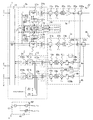
実施の形態1及び実施の形態2においては、無線送信周波数と無線受信周波数とが異なるFDDシステム等に対する構成を示した。本実施の形態3においては、TDD(時分割方式)システム等における送受信装置の構成について示す。図3は本発明の実施の形態3における送受信装置を示すブロック構成図である。
In the first embodiment and the second embodiment, the configuration for the FDD system or the like in which the radio transmission frequency and the radio reception frequency are different has been described. In the third embodiment, a configuration of a transmission / reception apparatus in a TDD (time division method) system or the like is described. FIG. 3 is a block configuration diagram showing a transmission / reception apparatus according to
本実施の形態3における送受信装置は、送信回路3aの方向性結合器35aの後段に、切替えスイッチ102aを有する構成としている。切替えスイッチ102aは、電力増幅器34aで電力増幅した無線送信信号をアンテナ8aへ供給するか、または、アンテナ8aから受信した無線受信信号を受信回路4aへ供給するかを選択する。送信回路3bについても、送信回路3aと同様の回路構成である。
The transmission / reception apparatus according to the third embodiment has a configuration in which a
受信回路4aは、実施の形態1における帰還回路4に相当する構成であるが、アンテナ8aから供給される無線受信信号を低雑音増幅する低雑音増幅器40aを有している。切替えスイッチ100aは、送信回路3aの方向性結合器35aから供給される無線送信信号とアンテナ8aを介して供給される無線受信信号とを切り替えている。受信回路4aは、スイッチ100aでの信号の選択により、受信信号処理と無線送信信号のフィードバック処理とを時分割で行っている。受信回路4bについても、受信回路4aと同様の回路構成である。
The reception circuit 4a has a configuration corresponding to the feedback circuit 4 in the first embodiment, but includes a
送信回路3aの方向性結合器35aで抽出された無線送信信号は、受信回路4a内の減衰器46aに帰還信号として入力される。減衰器46aにおいて所望の信号レベルに減衰した帰還信号は、切替えスイッチ100aに入力される。また、アンテナ8aで受信した無線受信信号は、切替えスイッチ102aを通過後、受信回路4a内の低雑音増幅器40aで低雑音増幅され、切替えスイッチ100aに入力される。受信回路4aの切替えスイッチ100aは、送受信タイミング信号に基づきスイッチを切替えることで、後段のミキサ47aに対して帰還信号(無線送信信号)と無線受信信号とを時分割で供給する。
The radio transmission signal extracted by the
ミキサ47aでは、可変信号発振器63から供給される搬送波(LO)により、帰還信号と無線受信信号とをそれぞれ中間周波数に変換する。TDDシステムの場合、無線送信周波数と無線受信周波数とは同一であることから、ミキサ47aから出力されるそれぞれの信号の周波数は同一であり、中間周波数に変換された帰還信号と受信信号とが時分割に出力される。
In the
後段の帯域通過フィルタ48aにおいて、不要な信号成分を除去した後、A/D変換器49aでサンプリング処理され、帰還信号はデジタル帰還信号(FB−IF1)として、受信信号はデジタル受信信号(RX−IF1)として受信信号処理回路12に時分割で供給される。
In the subsequent
受信信号処理回路12のデジタル直交復調回路120aは、A/D変換器49aから出力された信号をデジタル直交復調し、Iチャネル、Qチャネルのデジタルベースバンド信号I3、Q3を後段に接続される帰還信号選択回路74及びチャネル選択フィルタ121aに出力する。
The digital
1系の回路と同様の処理が2系の回路においても行われる。送信回路3bから供給される帰還信号と無線受信信号とは、受信回路4bで信号処理され、それぞれデジタル帰還信号(FB−IF2)とデジタル受信信号(RX−IF2)として受信信号処理回路12のデジタル直交復調回路120bへ時分割に供給される。デジタル直交復調回路120bにおいて、Iチャネル、Qチャネルのデジタルベースバンド信号I4、Q4を生成し、後段に接続される帰還信号選択回路74及びチャネル選択フィルタ121bに信号を供給する。
The same processing as that for the 1-system circuit is also performed for the 2-system circuit. The feedback signal and the radio reception signal supplied from the
チャネル選択フィルタ121a、121bに入力されたデジタルベースバンド信号はそれぞれ、妨害波信号成分を除去した後に、デジタルAGC回路122a、122bでそれぞれレベル補正を行なった後、ベースバンド信号処理回路11に供給される。ベースバンド信号処理回路11は、送受信タイミング信号に基づき、受信回路4a、4bが切替えスイッチ100a、100bで無線受信信号を選択するタイミングで、デジタルAGC回路122a、122bから供給される信号を信号処理して受信データを生成する。
The digital baseband signals input to the
受信回路4aの切替えスイッチ100aにおいて帰還信号が選択されたときにデジタル直交復調回路120aが出力するIチャネル、Qチャネルのデジタルベースバンド信号を帰還信号1と称する。同様に、受信回路4bの切替えスイッチ100bにおいて帰還信号が選択されたときにデジタル直交復調回路120bが出力するIチャネル、Qチャネルのデジタルベースバンド信号を帰還信号2と称する。
The I-channel and Q-channel digital baseband signals output by the digital
帰還信号選択回路74は、デジタル直交復調回路120a、120bから帰還信号1、帰還信号2がそれぞれ出力されるときに、どちらか一方を選択し、低域通過フィルタ72に供給する。低域通過フィルタ72で不要波信号を除去した帰還信号は、歪補償係数算出処理回路71に入力される。歪補償係数算出処理回路71では、信号選択回路70から供給される参照信号と低域通過フィルタ72から供給される帰還信号とを比較することで歪補償係数を算出し、一定の周期で歪補償テーブル23a、23bの補償テーブルを更新する。
When the
帰還信号選択回路74において選択される系統と、信号選択回路70において選択される系統とは一致している。例えば、帰還信号選択回路74において1系の受信回路4aから供給される帰還信号1が選択されるときは、信号選択回路70において1系の歪補償処理回路2aから供給される信号が選択される。
The system selected by the feedback
また、歪補償係数算出処理回路71で算出された歪補償係数は、帰還信号選択回路74及び信号選択回路70で選択された系統と同一の系統の歪補償テーブルに対して、所定の周期で時分割に供給される。例えば、帰還信号選択回路74及び信号選択回路70において1系が選択されるときは、歪補償係数算出処理回路71は1系の歪補償テーブル23aに対して歪補償係数を供給する。
In addition, the distortion compensation coefficient calculated by the distortion compensation coefficient
本実施の形態3における送受信装置は、各系統に対する歪補償係数の演算処理を歪補償係数算出回路7において時分割に行っている。このため、複数の系統で歪補償係数算出回路7を共通化することが可能となり、回路規模、部品点数を削減できるという効果を奏する。
In the transmission / reception apparatus according to the third embodiment, the distortion compensation
また、受信回路4a、4bにおいて、無線送信信号のフィードバック処理と受信処理とを時分割で行い、帰還回路と受信回路とを共通化しているため、更に回路規模、部品点数を削減できるという効果を奏する。これにより、装置の小型化・低消費電力化・低価格化が可能となる。
Further, in the receiving
実施の形態4.
実施の形態3では送信回路3a、3bにおいてアナログ直交変調を実施する構成としていたが、デジタル信号処理回路1においてデジタル直交変調を実施する構成としても良い。図4は本発明の実施の形態4における送受信装置を示すブロック構成図である。
Embodiment 4 FIG.
In the third embodiment, the analog quadrature modulation is performed in the
本実施の形態4における送受信装置は、歪補償処理回路2aの複素演算処理回路21aの後段にデジタル直交変調回路24aを備え、その後段に接続される送信回路3aにおいてアナログ直交変調器32aに換えてミキサ37aを配置している。送信回路3a内でD/A変換器31aとミキサ37aにより無線送信信号を生成し、電力増幅器34aに供給する構成となっている。また、歪補償処理回路2b及び送信回路3bについても同様の構成となっている。
The transmission / reception apparatus according to the fourth embodiment includes a digital
実施の形態2において説明したとおり、デジタルプリディストータ方式に代表される歪補償では、電力増幅器34a、34bにおいて発生する振幅・位相誤差を正確に抽出できれば、歪補償量を改善することができる。
As described in the second embodiment, in the distortion compensation typified by the digital predistorter method, the distortion compensation amount can be improved if the amplitude / phase errors generated in the
本実施の形態4によれば、実施の形態3と同様の効果を得ることができる。更に、アナログ直交変調器32a、32bの換わりにデジタル直交変調回路24a、24bを用いることで直交度誤差を低減している。このため、電力増幅器34a、34bにおいて発生する振幅・位相誤差を正確に抽出することができ、歪補償量を更に改善することができる。
According to the fourth embodiment, the same effect as in the third embodiment can be obtained. Further, by using digital
2a、2b 歪補償処理回路
3a、3b 送信回路
4 帰還回路
4a、4b 受信回路
7 歪補償係数算出回路
34a、34b 電力増幅器
2a, 2b Distortion
Claims (4)
前記複数の送信回路の中から選択した送信回路の送信信号に基づき帰還信号を生成する帰還回路と、
前記帰還信号に基づき歪補償係数を算出する歪補償係数算出回路と、
前記複数の送信回路それぞれに対応する複数の歪補償処理回路とを備え、
前記歪補償係数算出回路は、前記帰還回路で選択した送信回路に対応する歪補償処理回路に対して前記歪補償係数を出力し、
前記複数の歪補償処理回路はそれぞれ、前記歪補償係数に基づき送信ベースバンド信号を歪補償処理する送信機。 A plurality of transmission circuits for transmitting transmission signals amplified by the power amplifier;
A feedback circuit that generates a feedback signal based on a transmission signal of the transmission circuit selected from the plurality of transmission circuits;
A distortion compensation coefficient calculation circuit for calculating a distortion compensation coefficient based on the feedback signal;
A plurality of distortion compensation processing circuits corresponding to each of the plurality of transmission circuits,
The distortion compensation coefficient calculation circuit outputs the distortion compensation coefficient to a distortion compensation processing circuit corresponding to the transmission circuit selected by the feedback circuit,
The plurality of distortion compensation processing circuits each perform distortion compensation processing on a transmission baseband signal based on the distortion compensation coefficient.
前記送信信号と受信信号とから一方の信号を選択し、前記送信信号を選択したときに帰還信号を出力する複数の受信回路と、
前記複数の受信回路の中から選択した受信回路から出力された帰還信号に基づき、歪補償係数を算出する歪補償係数算出回路と、
前記複数の送信回路それぞれに対応する複数の歪補償処理回路とを備え、
前記歪補償係数算出回路は、前記選択した受信回路に対して送信信号を供給する送信回路に対応する歪補償処理回路に対して前記歪補償係数を出力し、
前記複数の歪補償処理回路はそれぞれ、前記歪補償係数に基づき送信ベースバンド信号を歪補償処理する送受信装置。 A plurality of transmission circuits for transmitting transmission signals amplified by the power amplifier;
Selecting one signal from the transmission signal and the reception signal, a plurality of reception circuits for outputting a feedback signal when the transmission signal is selected;
A distortion compensation coefficient calculating circuit that calculates a distortion compensation coefficient based on a feedback signal output from a receiving circuit selected from the plurality of receiving circuits;
A plurality of distortion compensation processing circuits corresponding to each of the plurality of transmission circuits,
The distortion compensation coefficient calculation circuit outputs the distortion compensation coefficient to a distortion compensation processing circuit corresponding to a transmission circuit that supplies a transmission signal to the selected reception circuit;
Each of the plurality of distortion compensation processing circuits performs distortion compensation processing on a transmission baseband signal based on the distortion compensation coefficient.
Priority Applications (1)
| Application Number | Priority Date | Filing Date | Title |
|---|---|---|---|
| JP2008202851A JP5151785B2 (en) | 2008-08-06 | 2008-08-06 | Transmitter and transmitter / receiver |
Applications Claiming Priority (1)
| Application Number | Priority Date | Filing Date | Title |
|---|---|---|---|
| JP2008202851A JP5151785B2 (en) | 2008-08-06 | 2008-08-06 | Transmitter and transmitter / receiver |
Publications (2)
| Publication Number | Publication Date |
|---|---|
| JP2010041470A true JP2010041470A (en) | 2010-02-18 |
| JP5151785B2 JP5151785B2 (en) | 2013-02-27 |
Family
ID=42013526
Family Applications (1)
| Application Number | Title | Priority Date | Filing Date |
|---|---|---|---|
| JP2008202851A Expired - Fee Related JP5151785B2 (en) | 2008-08-06 | 2008-08-06 | Transmitter and transmitter / receiver |
Country Status (1)
| Country | Link |
|---|---|
| JP (1) | JP5151785B2 (en) |
Cited By (9)
| Publication number | Priority date | Publication date | Assignee | Title |
|---|---|---|---|---|
| JP2013046365A (en) * | 2011-08-26 | 2013-03-04 | Fujitsu Ltd | Radio transmission device |
| WO2013069087A1 (en) * | 2011-11-07 | 2013-05-16 | 富士通株式会社 | Distortion compensating circuit and distortion compensating method |
| JP2014525712A (en) * | 2011-08-26 | 2014-09-29 | クゥアルコム・インコーポレイテッド | Adaptive interference cancellation for calibration against transmit distortion in multiple antenna transmitters |
| JP2014534704A (en) * | 2011-10-14 | 2014-12-18 | クゥアルコム・インコーポレイテッドQualcomm Incorporated | Adaptive transmitter predistortion that reuses an existing receiver for feedback |
| WO2016084650A1 (en) * | 2014-11-25 | 2016-06-02 | 住友電気工業株式会社 | Active antenna system |
| JP6056956B2 (en) * | 2013-03-15 | 2017-01-11 | 日本電気株式会社 | Communication apparatus and distortion suppression method thereof |
| US9793995B2 (en) | 2015-09-28 | 2017-10-17 | Fujitsu Limited | Communication device that transmits signals via a plurality of antennas and communication system |
| WO2018146741A1 (en) * | 2017-02-08 | 2018-08-16 | 日本電気株式会社 | Transmitter, communication system, control method and programm |
| WO2018199233A1 (en) * | 2017-04-27 | 2018-11-01 | 日本電気株式会社 | Transmitter, communication system, and method and program for controlling transmitter |
Citations (7)
| Publication number | Priority date | Publication date | Assignee | Title |
|---|---|---|---|---|
| JP2001268150A (en) * | 2000-03-21 | 2001-09-28 | Hitachi Kokusai Electric Inc | Linearizer |
| JP2004015310A (en) * | 2002-06-05 | 2004-01-15 | Mitsubishi Electric Corp | Distortion compensating circuit and transmitter |
| JP2004328710A (en) * | 2003-04-07 | 2004-11-18 | Hitachi Kokusai Electric Inc | Transmitting amplifier |
| JP2005033535A (en) * | 2003-07-14 | 2005-02-03 | Fujitsu Ten Ltd | Radio equipment |
| JP2006094043A (en) * | 2004-09-22 | 2006-04-06 | Matsushita Electric Ind Co Ltd | Transmission apparatus and communication apparatus |
| JP2006211701A (en) * | 2006-03-03 | 2006-08-10 | Fujitsu Ltd | Envelope detection type linearizer unit and distortion compensation updating method for use in the linearizer unit |
| US20080144539A1 (en) * | 2006-12-14 | 2008-06-19 | Texas Instruments Incorporated | Simplified Digital Predistortion in a Time-Domain Duplexed Transceiver |
-
2008
- 2008-08-06 JP JP2008202851A patent/JP5151785B2/en not_active Expired - Fee Related
Patent Citations (7)
| Publication number | Priority date | Publication date | Assignee | Title |
|---|---|---|---|---|
| JP2001268150A (en) * | 2000-03-21 | 2001-09-28 | Hitachi Kokusai Electric Inc | Linearizer |
| JP2004015310A (en) * | 2002-06-05 | 2004-01-15 | Mitsubishi Electric Corp | Distortion compensating circuit and transmitter |
| JP2004328710A (en) * | 2003-04-07 | 2004-11-18 | Hitachi Kokusai Electric Inc | Transmitting amplifier |
| JP2005033535A (en) * | 2003-07-14 | 2005-02-03 | Fujitsu Ten Ltd | Radio equipment |
| JP2006094043A (en) * | 2004-09-22 | 2006-04-06 | Matsushita Electric Ind Co Ltd | Transmission apparatus and communication apparatus |
| JP2006211701A (en) * | 2006-03-03 | 2006-08-10 | Fujitsu Ltd | Envelope detection type linearizer unit and distortion compensation updating method for use in the linearizer unit |
| US20080144539A1 (en) * | 2006-12-14 | 2008-06-19 | Texas Instruments Incorporated | Simplified Digital Predistortion in a Time-Domain Duplexed Transceiver |
Cited By (12)
| Publication number | Priority date | Publication date | Assignee | Title |
|---|---|---|---|---|
| JP2013046365A (en) * | 2011-08-26 | 2013-03-04 | Fujitsu Ltd | Radio transmission device |
| JP2014525712A (en) * | 2011-08-26 | 2014-09-29 | クゥアルコム・インコーポレイテッド | Adaptive interference cancellation for calibration against transmit distortion in multiple antenna transmitters |
| JP2014534704A (en) * | 2011-10-14 | 2014-12-18 | クゥアルコム・インコーポレイテッドQualcomm Incorporated | Adaptive transmitter predistortion that reuses an existing receiver for feedback |
| WO2013069087A1 (en) * | 2011-11-07 | 2013-05-16 | 富士通株式会社 | Distortion compensating circuit and distortion compensating method |
| JP6056956B2 (en) * | 2013-03-15 | 2017-01-11 | 日本電気株式会社 | Communication apparatus and distortion suppression method thereof |
| WO2016084650A1 (en) * | 2014-11-25 | 2016-06-02 | 住友電気工業株式会社 | Active antenna system |
| US9793995B2 (en) | 2015-09-28 | 2017-10-17 | Fujitsu Limited | Communication device that transmits signals via a plurality of antennas and communication system |
| WO2018146741A1 (en) * | 2017-02-08 | 2018-08-16 | 日本電気株式会社 | Transmitter, communication system, control method and programm |
| US10778264B2 (en) | 2017-02-08 | 2020-09-15 | Nec Corporation | Transmitter, communication system, control method, and program |
| WO2018199233A1 (en) * | 2017-04-27 | 2018-11-01 | 日本電気株式会社 | Transmitter, communication system, and method and program for controlling transmitter |
| JPWO2018199233A1 (en) * | 2017-04-27 | 2020-03-12 | 日本電気株式会社 | Transmitter, communication system, transmitter control method and program |
| US10749480B2 (en) | 2017-04-27 | 2020-08-18 | Nec Corporation | Transmitter, communication system, and method and program for controlling transmitter |
Also Published As
| Publication number | Publication date |
|---|---|
| JP5151785B2 (en) | 2013-02-27 |
Similar Documents
| Publication | Publication Date | Title |
|---|---|---|
| JP5151785B2 (en) | Transmitter and transmitter / receiver | |
| JP5608939B2 (en) | Receiver, transmitter, feedback device, transceiver, and signal processing method | |
| US7783263B2 (en) | Simplified digital predistortion in a time-domain duplexed transceiver | |
| US6934341B2 (en) | Method and apparatus for plurality signal generation | |
| EP2892193B1 (en) | I/Q-mismatch compensation method and apparatus | |
| US8831543B2 (en) | Method and system for a linearized transmitter including a power amplifier | |
| US20080139141A1 (en) | Method and system for estimating and compensating non-linear distortion in a transmitter using data signal feedback | |
| US9596120B2 (en) | Signal transmission apparatus, distortion compensation apparatus, and signal transmission method | |
| US8908746B2 (en) | Method and apparatus to use auxiliary receiver to compensate multiple transmitters based upon one of the transmitters | |
| JP4901679B2 (en) | Wireless transmission / reception device and wireless transmission method | |
| JP2006148940A (en) | Inphase/quadrature phase imbalance compensation | |
| CN111865353A (en) | RF front end with reduced receiver desensitization | |
| WO2006118317A1 (en) | Polar modulation transmitter circuit and communications device | |
| US8090036B2 (en) | Transmitter and carrier leak detection method | |
| US20140232468A1 (en) | Suppression circuit for suppressing unwanted transmitter output | |
| JP2007104007A (en) | Orthogonal modulator, and vector correction method in the same | |
| US8903014B2 (en) | Communications device having controller to correct an initial IQ imbalance and associated methods | |
| JP2019057878A (en) | Carrier leak compensation method in orthogonal modulator | |
| JP4587893B2 (en) | Transceiver | |
| KR20100039255A (en) | Apparatus and method for compensating iq mismatch in portable communication system | |
| US9991994B1 (en) | Method and terminal device for reducing image distortion | |
| JP2006094043A (en) | Transmission apparatus and communication apparatus | |
| JP2002152289A (en) | Distortion compensation device | |
| KR20230029921A (en) | Apparatus and methods for wireless transmitters | |
| CN112042114B (en) | Radio frequency receiver, radio frequency transmitter and communication equipment |
Legal Events
| Date | Code | Title | Description |
|---|---|---|---|
| A621 | Written request for application examination |
Free format text: JAPANESE INTERMEDIATE CODE: A621 Effective date: 20110126 |
|
| A131 | Notification of reasons for refusal |
Free format text: JAPANESE INTERMEDIATE CODE: A131 Effective date: 20120313 |
|
| A521 | Written amendment |
Free format text: JAPANESE INTERMEDIATE CODE: A523 Effective date: 20120511 |
|
| A131 | Notification of reasons for refusal |
Free format text: JAPANESE INTERMEDIATE CODE: A131 Effective date: 20120605 |
|
| A521 | Written amendment |
Free format text: JAPANESE INTERMEDIATE CODE: A523 Effective date: 20120803 |
|
| A131 | Notification of reasons for refusal |
Free format text: JAPANESE INTERMEDIATE CODE: A131 Effective date: 20120821 |
|
| A521 | Written amendment |
Free format text: JAPANESE INTERMEDIATE CODE: A523 Effective date: 20121016 |
|
| TRDD | Decision of grant or rejection written | ||
| A01 | Written decision to grant a patent or to grant a registration (utility model) |
Free format text: JAPANESE INTERMEDIATE CODE: A01 Effective date: 20121106 |
|
| A61 | First payment of annual fees (during grant procedure) |
Free format text: JAPANESE INTERMEDIATE CODE: A61 Effective date: 20121119 |
|
| FPAY | Renewal fee payment (event date is renewal date of database) |
Free format text: PAYMENT UNTIL: 20151214 Year of fee payment: 3 |
|
| R151 | Written notification of patent or utility model registration |
Ref document number: 5151785 Country of ref document: JP Free format text: JAPANESE INTERMEDIATE CODE: R151 |
|
| FPAY | Renewal fee payment (event date is renewal date of database) |
Free format text: PAYMENT UNTIL: 20151214 Year of fee payment: 3 |
|
| R250 | Receipt of annual fees |
Free format text: JAPANESE INTERMEDIATE CODE: R250 |
|
| R250 | Receipt of annual fees |
Free format text: JAPANESE INTERMEDIATE CODE: R250 |
|
| R250 | Receipt of annual fees |
Free format text: JAPANESE INTERMEDIATE CODE: R250 |
|
| LAPS | Cancellation because of no payment of annual fees |