JP2010039824A - Settlement device - Google Patents
Settlement device Download PDFInfo
- Publication number
- JP2010039824A JP2010039824A JP2008202971A JP2008202971A JP2010039824A JP 2010039824 A JP2010039824 A JP 2010039824A JP 2008202971 A JP2008202971 A JP 2008202971A JP 2008202971 A JP2008202971 A JP 2008202971A JP 2010039824 A JP2010039824 A JP 2010039824A
- Authority
- JP
- Japan
- Prior art keywords
- loop antenna
- display device
- settlement apparatus
- payment
- view
- Prior art date
- Legal status (The legal status is an assumption and is not a legal conclusion. Google has not performed a legal analysis and makes no representation as to the accuracy of the status listed.)
- Granted
Links
Images


Abstract
Description
本発明は、非接触ICカード等の非接触通信媒体と通信し決済を行うための決済装置に関するものである。 The present invention relates to a settlement apparatus for performing settlement by communicating with a non-contact communication medium such as a non-contact IC card.
クレジット機能、プリペイド機能、デビット機能を備える非接触ICカードが少額決済の用途に使用されている。非接触ICカードと通信して決済を行う決済装置には、一般的にループアンテナと、該ループアンテナを通じて非接触ICカードと通信する通信回路とを備えている。更に、該決済装置は、決済情報等を表示するための表示部を備え、該表示部を介して操作の誘導を行っている。特許文献1には、表示装置の周囲にループアンテナを配置した電子機器が開示されている。
非接触通信技術を用いる決済装置においては、操作性の改善のため、特許文献1に開示されているようにループアンテナの中央に、操作の誘導情報を表示する表示装置を配置することが望ましい。しかしながら、ハンディータイプのように小型化させた決済装置において、ループアンテナの中央に表示装置を配置すると、ループアンテナを設けない装置に比べて表示装置を小さくせざるを得ず、操作誘導の表示が行い難くなる課題が生じる。 In a settlement apparatus using contactless communication technology, it is desirable to arrange a display device that displays operation guidance information in the center of the loop antenna as disclosed in Patent Document 1 in order to improve operability. However, in a settlement device reduced in size such as a handy type, if a display device is arranged in the center of the loop antenna, the display device must be made smaller than a device that does not provide a loop antenna, and an operation guidance display is possible. There are challenges that are difficult to do.
本発明は、上述した課題を解決するためになされたものであり、その目的とするところは、表示装置の表示面と平行な面上にループアンテナを配置し、面上に該ループアンテナの占める面積を最小にできる決済装置を提供することにある。 The present invention has been made to solve the above-described problems, and an object of the present invention is to arrange a loop antenna on a surface parallel to the display surface of the display device, and occupy the loop antenna on the surface. An object of the present invention is to provide a settlement apparatus that can minimize the area.
上記目的を達成するため、請求項1の発明は、表示装置46を備え、ループアンテナ56を備える決済媒体80に対して通信により決済を行うための決済装置10であって、
前記表示装置46の周囲に、平面状のフレキシブル基板56Fから成るループアンテナ56の少なくとも一部を前記表示装置46の表示面の垂直方向に折り曲げて配置したことを技術的特徴とする。
In order to achieve the above object, the invention of claim 1 is a
A technical feature is that at least a part of the
請求項1の決済装置では、表示装置の周囲にループアンテナを設けるため、表示装置に決済媒体を対応させることで、通信を行うことができる。ここで、平面状のフレキシブル基板から成るループアンテナの少なくとも一部を表示装置の表示面の垂直方向に折り曲げて配置することで、表示装置の表示面と平行な面上に該ループアンテナの占める面積を小さくすることができる。 In the settlement apparatus according to the first aspect, since the loop antenna is provided around the display device, communication can be performed by making the settlement medium correspond to the display device. Here, an area occupied by the loop antenna on a plane parallel to the display surface of the display device by disposing at least a part of the loop antenna formed of a flat flexible substrate in a direction perpendicular to the display surface of the display device. Can be reduced.
請求項2の決済装置では、平面状のフレキシブル基板から成るループアンテナの全部を表示装置の表示面の垂直方向に折り曲げて配置することで、表示装置の表示面と平行な面上に該ループアンテナの占める面積を最小にできる。 According to another aspect of the present invention, the loop antenna is formed on a plane parallel to the display surface of the display device by arranging all of the loop antennas made of a flat flexible substrate in a direction perpendicular to the display surface of the display device. The area occupied by can be minimized.
請求項3の決済装置では、ループアンテナを、筐体の立壁の内周に沿って配置することで、ループ径を大きくすることができる。 In the settlement apparatus according to the third aspect, the loop diameter can be increased by arranging the loop antenna along the inner periphery of the standing wall of the casing.
[第1実施形態]
以下、本発明の第1実施形態に係る決済装置について図を参照して説明する。
第1実施形態の決済装置10は、使用者が手で持って操作するハンディータイプであって、商品に付けられたバーコード、二次元コード等の光学情報を読み取り、商品の売り上げ額(支払額)を算出すると共に、該売り上げ額の払いを、プリペイド機能又はクレジット機能を備える非接触ICカード、ICチップを内蔵する携帯電話で行わしめ決済するものである。
[First embodiment]
Hereinafter, a settlement apparatus according to a first embodiment of the present invention will be described with reference to the drawings.
The
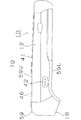
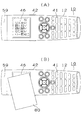
図1は決済装置の側面図であり、図2(A)は平面図である。
決済装置10は握り部を兼用する操作部12、液晶表示装置46などを備えている。操作部12には、例えば複数のキースイッチ41が設けられ、これらキースイッチ41により、動作内容を指示するようになっている。この操作部12には、キースイッチ41に加えて、読み取り開始を指示するためのトリガースイッチ42が設けられている。決済装置10の筐体59の前端に形成された図1に示す略矩形の開口部(読取口)18には後述する光学系ユニットが配置されている。また、液晶表示装置46の周囲には後述するループアンテナが配置されている。
FIG. 1 is a side view of the settlement apparatus, and FIG. 2 (A) is a plan view.
The
決済装置10の回路構成を図3のブロック図を参照して説明する。
決済装置10は、バーコード、二次元コード等の光学情報の読み取りと、非接触ICカード等の無線情報媒体の情報を無線で読み取り書き込みが可能なように構成されている。決済装置10には、回路部20が設けられている。回路部20は、主に、発光ダイオード21、集光レンズ24、受光センサ23、結像レンズ27等の光学系と、ループアンテナ56、インピーダンス整合回路58、送信回路54、受信回路52からなる無線系と、メモリ35、制御回路40、キースイッチ41、トリガースイッチ42、液晶表示装置46等のマイクロコンピュータ(以下「マイコン」という)系と、から構成されている。
The circuit configuration of the
The
まず、光学系から説明する。発光ダイオード21は、照明光Lfを照射可能な光照射器として機能するもので、拡散レンズと凸レンズとを組み合わせた集光レンズ24により集光させる。受光センサ23は、読取対象物RやバーコードBに照射されて反射した反射光Lrを結像レンズ27を介して受光可能に構成されるイメージセンサから成る。結像レンズ27は、外部から入射する入射光を集光して受光センサ23の受光面23aに像を結像可能な結像光学系として機能する。
First, the optical system will be described. The
次に、マイコン系の構成概要を説明する。マイコン系は、増幅回路31、A/D変換回路33、メモリ35、アドレス発生回路36、同期信号発生回路38、制御回路40、キースイッチ41、トリガースイッチ42、LED43、ブザー44、液晶表示装置46、通信部48等から構成されている。このマイコン系は、その名の通り、マイコン(情報処理装置)として機能し得る制御回路40およびメモリ35を中心に構成されるもので、前述した光学系によって撮像された画像信号をハードウェア的およびソフトウェア的に信号処理し得るものである。また制御回路40は、当該決済装置10の全体システムに関する制御も行っている。
Next, a configuration outline of the microcomputer system will be described. The microcomputer system includes an
光学系の受光センサ23から出力される画像信号(アナログ信号)は、増幅回路31に入力されることで所定ゲインで増幅された後、A/D変換回路33に入力されると、アナログ信号からディジタル信号に変換される。そして、ディジタル化された画像信号、つまり画像データは、メモリ35に入力されて蓄積される。なお、同期信号発生回路38は、受光センサ23およびアドレス発生回路36に対する同期信号を発生可能に構成されており、またアドレス発生回路36は、この同期信号発生回路38から供給される同期信号に基づいて、メモリ35に格納される画像データの格納アドレスを発生可能に構成されている。
An image signal (analog signal) output from the
制御回路40は、決済装置10全体を制御可能なマイコンで、CPU、システムバス、入出力インタフェース等からなるもので、メモリ35とともに情報処理装置を構成し得るもので情報処理機能を有する。この制御回路40には、内蔵された入出力インタフェースを介して種々の入出力装置(周辺装置)と接続可能に構成されており、本実施形態の場合、キースイッチ41、トリガースイッチ42、LED43、ブザー44、液晶表示装置46、通信部48等が接続されている。制御回路40は、二次元コードを読み取った結果及び決済の情報を、通信部48を介して図1を参照して上述した端末管理装置60側へ出力するよう構成されている。
The
ループアンテナ56、インピーダンス整合回路58、送信回路54、受信回路52からなる無線系50は、例えばプリペイド機能を備える非接触ICカードとの間で電磁波(例えば、マイクロ波やHF帯の周波数の電波)による通信を行って電力の供給及びデータの読み取りを行うためのものである。ここでは、データの読み取りだけでなく、非接触ICカードに対するデータの書き込みも行う。
The
無線系50を構成する送信回路54、受信回路52は、制御回路40により制御される。制御回路40は、送信回路54を介してループアンテナ56に電力信号を出力するとともに、ループアンテナ56が受け取った受信信号を、受信回路52を介して復調してデータとして抽出する。これにより、ループアンテナ56に読み取るべき非接触ICカードが近づけられた状態で、該非接触ICカードに対して、電波により電力供給が行われると共に、データの通信(書き込み及び読み取り)が行われるようになっている。
The
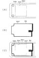
インピーダンス整合回路58は、ループアンテナのインピーダンスを調整するためのものである。図4(A)中にインピーダンス整合回路の回路図を示す。ループアンテナ56に並列に可変容量コンデンサC2が接続され、該ループアンテナ56及び可変容量コンデンサC2と直列に可変容量コンデンサC1が接続されている。図4(B)は、別例を示す。ループアンテナ56と直列に可変容量コンデンサC4が接続され、該ループアンテナ56及び可変容量コンデンサC4に並列に可変容量コンデンサC3が接続されている。第1実施形態の決済装置では、使用周波数に対して径の小さなループアンテナ56を用いても、インピーダンス整合回路58により効率的に電波を送受できる。
The impedance matching
なお、周知なように、非接触ICカードは、無線系の給電用信号から動作電源を得るための整流・平滑回路、通信等の制御を行うCPU、送受信信号の変調・復調を行う変復調回路、動作プログラム等を記憶するROM、データを記憶する読書き可能なEEPROM等をワンチップ化したICを内蔵している。また、無線決済に対応し得る携帯電話は、該ICチップを内蔵している。 As is well known, the non-contact IC card includes a rectifying / smoothing circuit for obtaining an operating power supply from a wireless power supply signal, a CPU for controlling communication, a modulation / demodulating circuit for modulating / demodulating transmission / reception signals, It has a built-in IC in which a ROM for storing operation programs and the like, a readable / writable EEPROM for storing data, etc. are made into one chip. In addition, a mobile phone that can handle wireless payment has the IC chip built-in.
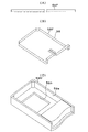
図5(A)は、第1実施形態の決済装置のループアンテナ56を構成するフレキシブル基板の平面図であり、図5(B)は側面図である。図5(C)は液晶表示装置46にフレキシブル基板56Fを取り付けた状態の平面図であり、図5(D)は側面図である。
フレキシブル基板56Fは、矩形形状(山折り線を構成する二点鎖線)の4隅に設けられる三角部56Dと、矩形形状から延在する長方形部56Sとからなり、ループアンテナ56を構成する配線を内蔵する樹脂等の誘電板から構成されている。ここで、矩形形状から延在する長方形部56Sを直角(液晶表示装置46の表示面の垂直方向)に曲げてループアンテナ56を液晶表示装置の外周に配置することで、図5(C)に示すように液晶表示装置46の表示面と平行な面上に該ループアンテナ56の占める面積を小さくすることができる。
FIG. 5A is a plan view of a flexible substrate constituting the
The
第1実施形態の決済装置10では、液晶表示装置46の周囲にループアンテナ56を設けるため、液晶表示装置46に非接触ICカード、ICチップを内蔵する携帯電話を対応させることで、通信を行うことができる。即ち、使用者は、図1中に示す決済装置10の読取口18を商品に付けられたバーコード、二次元コードに向けてトリガースイッチを操作することで、該決済装置10は、バーコード、二次元コードを読み取り商品の売り上げ額(支払額)を算出する。そして、支払い額を液晶表示装置46に表示した後、図2(A)に示すようにプリペイド機能又はクレジット機能を備える非接触ICカード、ICチップを内蔵する携帯電話を液晶表示装置(画面)46に当てることを案内する表示[この画面にICカード、携帯電話をあててください]等の表示を行う。これに応じて、図2(B)に示すように、支払者が非接触ICカード80を液晶表示装置46に対向させることで、該決済装置10と非接触ICカード80との間の通信が可能になり、決済装置10は無線通信を介して決済を行う。
In the
ここで、既存の光学情報及びIFタグに対応し得る情報コード読取装置の場合、IFタグとの通信用のアンテナが読取口側に設けられているため、該情報コード読取装置を用いて決済装置を構成した場合には、非接触ICカード、携帯電話に向けて読取口を向けることになるため操作が非常に困難である。容易に操作を行うためには、使用者が支払者から携帯電話等を預かり、決済装置の読取口を当てる必要があり、この場合、携帯電話を落とす等のトラブルが予想される。これに対して、第1実施形態では、支払者が決済装置10の液晶表示装置46に非接触ICカード、携帯電話をかざすことで決済が行えるので、操作が容易である。更に、ハンディータイプ、即ち、小型で横幅の狭い決済装置で、ループアンテナ56の占める面積を狭くできるので、液晶表示装置46を大きくすることができ、種々の案内情報を大きな文字で表示することが可能である。
Here, in the case of an information code reader that can handle existing optical information and IF tags, since an antenna for communication with the IF tag is provided on the reading port side, a payment device using the information code reader is used. Is difficult to operate because the reading port faces the non-contact IC card or mobile phone. In order to perform the operation easily, it is necessary for the user to take a mobile phone or the like from the payer and touch the reading port of the settlement apparatus. In this case, troubles such as dropping the mobile phone are expected. On the other hand, in the first embodiment, the payer can make a payment by holding the non-contact IC card or the mobile phone over the liquid
[第2実施形態]
引き続き、本発明の第2実施形態に係る決済装置について図6を参照して説明する。
第2実施形態の決済装置は、ループアンテナの構成を除き、図1〜図4を参照して上述した第1実施形態と同様であるため、ループアンテナの構成について図6を参照して説明する。
図6(A)は、第2実施形態の決済装置のループアンテナを構成するフレキシブル基板の平面図であり、図6(B)は側面図である。図6(C)は液晶表示装置にフレキシブル基板を取り付けた状態の平面図であり、図6(D)は側面図である。
[Second Embodiment]
Next, a settlement apparatus according to the second embodiment of the present invention will be described with reference to FIG.
The settlement apparatus according to the second embodiment is the same as the first embodiment described above with reference to FIGS. 1 to 4 except for the configuration of the loop antenna. Therefore, the configuration of the loop antenna will be described with reference to FIG. .
FIG. 6A is a plan view of a flexible substrate constituting the loop antenna of the settlement apparatus of the second embodiment, and FIG. 6B is a side view. FIG. 6C is a plan view of a state in which a flexible substrate is attached to the liquid crystal display device, and FIG. 6D is a side view.
第2実施形態のループアンテナ56を構成するフレキシブル基板56Fは、矩形枠形状に構成され、短辺側を山折りすると共に、長辺側に対しては山折りと谷折りを組み合わせることで、図6(C)に示すように、フレキシブル基板56Fの全てを液晶表示装置46の表示面の垂直方向に曲げてループアンテナ56を液晶表示装置の外周に配置する。これにより、液晶表示装置46の表示面と平行な面上に該ループアンテナの占める面積を最小にしている。
The
第2実施形態の決済装置10では、液晶表示装置46の周囲にループアンテナ56を設けるため、液晶表示装置46に非接触ICカード、ICチップを内蔵する携帯電話を対応させることで、通信を行うことができる。
In the
[第3実施形態]
次に、本発明の第3実施形態に係る決済装置について図7、図8を参照して説明する。
第3実施形態の決済装置は、ループアンテナの構成を除き、図1〜図4を参照して上述した第1実施形態と同様であるため、ループアンテナの構成について図7及び図8を参照して説明する。
図1中に示す決済装置10の筐体59は、液晶表示装置46、キースイッチ41等の設けられる上側筐体59Uと、下側筐体59Lとを組み合わせてなる。図7(A)は、第3実施形態の決済装置の上側筐体59Uを内側からみた平面図であり、図7(B)は、ループアンテナ56を構成するフレキシブル基板56Fの平面図であり、図7(C)は、上側筐体59U内にループアンテ56を構成するフレキシブル基板56Fを配置した状態を示す平面図である。図8(A)は第3実施形態のループアンテナを構成する前のフレキシブル基板56Fの平面図であり、図8(B)はループアンテナ56の斜視図であり、図8(C)は上側筐体59Uの斜視図である。
[Third embodiment]
Next, a settlement apparatus according to a third embodiment of the present invention will be described with reference to FIGS.
The settlement apparatus of the third embodiment is the same as that of the first embodiment described above with reference to FIGS. 1 to 4 except for the configuration of the loop antenna, and therefore the configuration of the loop antenna is described with reference to FIGS. 7 and 8. I will explain.
A
上側筐体59Uには、中央部に液晶表示装置46を取り付けるための開口59bが穿設され、外周部に立壁59aが液晶表示装置46の垂直方向に形成されている。ループアンテナ56は、図7(C)に示すように該立壁59aの内周に沿って配置し得るように、図7(B)に示すよう、液晶表示装置46の垂直方向に曲げられ、該形状に形成されている。
The
第3実施形態の決済装置10では、ループアンテナ56を構成するフレキシブル基板56Fを、上側筐体59Uの立壁59aの内周に沿って配置するため、ループアンテナのループ径を大きくできる。これにより、効率的に非接触ICカード、携帯電話等と通信することが可能になる。
In the
上述した実施形態では、表示装置として液晶表示装置を用いたが、表示装置としては、例えば、LEDからなる表示装置を用いることも可能である。 In the embodiment described above, the liquid crystal display device is used as the display device. However, as the display device, for example, a display device made of LEDs can be used.
10 決済装置
46 液晶表示装置
56 ループアンテナ
56F フレキシブル基板
59 筐体
59a 立壁
80 非接触ICカード(決済媒体)
DESCRIPTION OF
Claims (3)
前記表示装置の周囲に、平面状のフレキシブル基板から成るループアンテナの少なくとも一部を前記表示装置の表示面の垂直方向に折り曲げて配置したことを特徴とする決済装置。 A payment device for payment by communication with a payment medium including a display device and a loop antenna,
A settlement apparatus characterized in that at least a part of a loop antenna made of a flat flexible substrate is bent around the display device in a direction perpendicular to the display surface of the display device.
Priority Applications (1)
| Application Number | Priority Date | Filing Date | Title |
|---|---|---|---|
| JP2008202971A JP5109860B2 (en) | 2008-08-06 | 2008-08-06 | Payment device |
Applications Claiming Priority (1)
| Application Number | Priority Date | Filing Date | Title |
|---|---|---|---|
| JP2008202971A JP5109860B2 (en) | 2008-08-06 | 2008-08-06 | Payment device |
Publications (2)
| Publication Number | Publication Date |
|---|---|
| JP2010039824A true JP2010039824A (en) | 2010-02-18 |
| JP5109860B2 JP5109860B2 (en) | 2012-12-26 |
Family
ID=42012292
Family Applications (1)
| Application Number | Title | Priority Date | Filing Date |
|---|---|---|---|
| JP2008202971A Active JP5109860B2 (en) | 2008-08-06 | 2008-08-06 | Payment device |
Country Status (1)
| Country | Link |
|---|---|
| JP (1) | JP5109860B2 (en) |
Cited By (3)
| Publication number | Priority date | Publication date | Assignee | Title |
|---|---|---|---|---|
| JP2013251499A (en) * | 2012-06-04 | 2013-12-12 | Nec Access Technica Ltd | Three-dimensional structure flexible printed wiring board and loop wiring formation method |
| JP2018146126A (en) * | 2017-03-01 | 2018-09-20 | 日油株式会社 | Transmission apparatus and radio detonation system |
| US10109914B2 (en) | 2015-03-27 | 2018-10-23 | Intel IP Corporation | Antenna system |
Citations (2)
| Publication number | Priority date | Publication date | Assignee | Title |
|---|---|---|---|---|
| JP2005026865A (en) * | 2003-06-30 | 2005-01-27 | Sony Corp | Data communication equipment |
| JP2007305656A (en) * | 2006-05-09 | 2007-11-22 | Sumitomo Bakelite Co Ltd | Coil member |
-
2008
- 2008-08-06 JP JP2008202971A patent/JP5109860B2/en active Active
Patent Citations (2)
| Publication number | Priority date | Publication date | Assignee | Title |
|---|---|---|---|---|
| JP2005026865A (en) * | 2003-06-30 | 2005-01-27 | Sony Corp | Data communication equipment |
| JP2007305656A (en) * | 2006-05-09 | 2007-11-22 | Sumitomo Bakelite Co Ltd | Coil member |
Cited By (3)
| Publication number | Priority date | Publication date | Assignee | Title |
|---|---|---|---|---|
| JP2013251499A (en) * | 2012-06-04 | 2013-12-12 | Nec Access Technica Ltd | Three-dimensional structure flexible printed wiring board and loop wiring formation method |
| US10109914B2 (en) | 2015-03-27 | 2018-10-23 | Intel IP Corporation | Antenna system |
| JP2018146126A (en) * | 2017-03-01 | 2018-09-20 | 日油株式会社 | Transmission apparatus and radio detonation system |
Also Published As
| Publication number | Publication date |
|---|---|
| JP5109860B2 (en) | 2012-12-26 |
Similar Documents
| Publication | Publication Date | Title |
|---|---|---|
| US9667761B2 (en) | System for and method of adapting a mobile device having a camera to a reader for electro-optically reading targets | |
| CN104392196B (en) | The remote selective RFID waken up is detected using laser optical | |
| JP2009015443A (en) | Radio tag reader-writer | |
| JP4692285B2 (en) | Portable information reader | |
| US20090166421A1 (en) | Rfid reader / card combination to convert a contact smartcard reader to contactless | |
| JP5109860B2 (en) | Payment device | |
| US20030012000A1 (en) | Portable information terminal | |
| KR101955661B1 (en) | Electronic tag reader | |
| JP5071064B2 (en) | Portable reader / writer | |
| US7830277B2 (en) | Method and apparatus for providing intrinsic information in mobile communication terminal | |
| JP2007004501A (en) | Electronic equipment | |
| WO2010134154A1 (en) | Optical communication system and optical communication method | |
| JP2009098951A (en) | Interrogator | |
| JP2007004502A (en) | Electronic equipment | |
| JP6458690B2 (en) | RFID reader | |
| JP7196672B2 (en) | Information reader | |
| EP3567515B1 (en) | Information reading apparatus | |
| JP2010257159A (en) | Non-contact ic card with display | |
| JP2009064307A (en) | Information display system | |
| JP3145468U (en) | Information processing device | |
| KR100654877B1 (en) | Interrogator of moving body identification device | |
| JP5092882B2 (en) | Information reader | |
| JP2004240715A (en) | Information processing apparatus and method, and program | |
| JP2010033162A (en) | Card processor and plane type antenna | |
| CN211698959U (en) | Hand-held type recognition equipment |
Legal Events
| Date | Code | Title | Description |
|---|---|---|---|
| A621 | Written request for application examination |
Free format text: JAPANESE INTERMEDIATE CODE: A621 Effective date: 20100727 |
|
| A977 | Report on retrieval |
Free format text: JAPANESE INTERMEDIATE CODE: A971007 Effective date: 20120618 |
|
| A131 | Notification of reasons for refusal |
Free format text: JAPANESE INTERMEDIATE CODE: A131 Effective date: 20120626 |
|
| A521 | Request for written amendment filed |
Free format text: JAPANESE INTERMEDIATE CODE: A523 Effective date: 20120821 |
|
| TRDD | Decision of grant or rejection written | ||
| A01 | Written decision to grant a patent or to grant a registration (utility model) |
Free format text: JAPANESE INTERMEDIATE CODE: A01 Effective date: 20120911 |
|
| A01 | Written decision to grant a patent or to grant a registration (utility model) |
Free format text: JAPANESE INTERMEDIATE CODE: A01 |
|
| A61 | First payment of annual fees (during grant procedure) |
Free format text: JAPANESE INTERMEDIATE CODE: A61 Effective date: 20120924 |
|
| FPAY | Renewal fee payment (event date is renewal date of database) |
Free format text: PAYMENT UNTIL: 20151019 Year of fee payment: 3 |
|
| R150 | Certificate of patent or registration of utility model |
Ref document number: 5109860 Country of ref document: JP Free format text: JAPANESE INTERMEDIATE CODE: R150 Free format text: JAPANESE INTERMEDIATE CODE: R150 |
|
| FPAY | Renewal fee payment (event date is renewal date of database) |
Free format text: PAYMENT UNTIL: 20151019 Year of fee payment: 3 |
|
| R250 | Receipt of annual fees |
Free format text: JAPANESE INTERMEDIATE CODE: R250 |
|
| R250 | Receipt of annual fees |
Free format text: JAPANESE INTERMEDIATE CODE: R250 |
|
| R250 | Receipt of annual fees |
Free format text: JAPANESE INTERMEDIATE CODE: R250 |
|
| R250 | Receipt of annual fees |
Free format text: JAPANESE INTERMEDIATE CODE: R250 |
|
| R250 | Receipt of annual fees |
Free format text: JAPANESE INTERMEDIATE CODE: R250 |
|
| R250 | Receipt of annual fees |
Free format text: JAPANESE INTERMEDIATE CODE: R250 |
|
| R250 | Receipt of annual fees |
Free format text: JAPANESE INTERMEDIATE CODE: R250 |
|
| R250 | Receipt of annual fees |
Free format text: JAPANESE INTERMEDIATE CODE: R250 |
|
| R250 | Receipt of annual fees |
Free format text: JAPANESE INTERMEDIATE CODE: R250 |