JP2010033675A - Semiconductor memory device - Google Patents
Semiconductor memory device Download PDFInfo
- Publication number
- JP2010033675A JP2010033675A JP2008196366A JP2008196366A JP2010033675A JP 2010033675 A JP2010033675 A JP 2010033675A JP 2008196366 A JP2008196366 A JP 2008196366A JP 2008196366 A JP2008196366 A JP 2008196366A JP 2010033675 A JP2010033675 A JP 2010033675A
- Authority
- JP
- Japan
- Prior art keywords
- wiring
- line
- column
- voltage
- control circuit
- Prior art date
- Legal status (The legal status is an assumption and is not a legal conclusion. Google has not performed a legal analysis and makes no representation as to the accuracy of the status listed.)
- Granted
Links
Images


Classifications
-
- G—PHYSICS
- G11—INFORMATION STORAGE
- G11C—STATIC STORES
- G11C11/00—Digital stores characterised by the use of particular electric or magnetic storage elements; Storage elements therefor
- G11C11/21—Digital stores characterised by the use of particular electric or magnetic storage elements; Storage elements therefor using electric elements
- G11C11/34—Digital stores characterised by the use of particular electric or magnetic storage elements; Storage elements therefor using electric elements using semiconductor devices
- G11C11/40—Digital stores characterised by the use of particular electric or magnetic storage elements; Storage elements therefor using electric elements using semiconductor devices using transistors
- G11C11/401—Digital stores characterised by the use of particular electric or magnetic storage elements; Storage elements therefor using electric elements using semiconductor devices using transistors forming cells needing refreshing or charge regeneration, i.e. dynamic cells
- G11C11/4063—Auxiliary circuits, e.g. for addressing, decoding, driving, writing, sensing or timing
- G11C11/407—Auxiliary circuits, e.g. for addressing, decoding, driving, writing, sensing or timing for memory cells of the field-effect type
- G11C11/408—Address circuits
- G11C11/4087—Address decoders, e.g. bit - or word line decoders; Multiple line decoders
-
- G—PHYSICS
- G11—INFORMATION STORAGE
- G11C—STATIC STORES
- G11C8/00—Arrangements for selecting an address in a digital store
- G11C8/08—Word line control circuits, e.g. drivers, boosters, pull-up circuits, pull-down circuits, precharging circuits, for word lines
-
- G—PHYSICS
- G11—INFORMATION STORAGE
- G11C—STATIC STORES
- G11C13/00—Digital stores characterised by the use of storage elements not covered by groups G11C11/00, G11C23/00, or G11C25/00
- G11C13/02—Digital stores characterised by the use of storage elements not covered by groups G11C11/00, G11C23/00, or G11C25/00 using elements whose operation depends upon chemical change
-
- G—PHYSICS
- G11—INFORMATION STORAGE
- G11C—STATIC STORES
- G11C13/00—Digital stores characterised by the use of storage elements not covered by groups G11C11/00, G11C23/00, or G11C25/00
-
- G—PHYSICS
- G11—INFORMATION STORAGE
- G11C—STATIC STORES
- G11C13/00—Digital stores characterised by the use of storage elements not covered by groups G11C11/00, G11C23/00, or G11C25/00
- G11C13/0002—Digital stores characterised by the use of storage elements not covered by groups G11C11/00, G11C23/00, or G11C25/00 using resistive RAM [RRAM] elements
- G11C13/0004—Digital stores characterised by the use of storage elements not covered by groups G11C11/00, G11C23/00, or G11C25/00 using resistive RAM [RRAM] elements comprising amorphous/crystalline phase transition cells
-
- G—PHYSICS
- G11—INFORMATION STORAGE
- G11C—STATIC STORES
- G11C13/00—Digital stores characterised by the use of storage elements not covered by groups G11C11/00, G11C23/00, or G11C25/00
- G11C13/0002—Digital stores characterised by the use of storage elements not covered by groups G11C11/00, G11C23/00, or G11C25/00 using resistive RAM [RRAM] elements
- G11C13/0009—RRAM elements whose operation depends upon chemical change
- G11C13/0011—RRAM elements whose operation depends upon chemical change comprising conductive bridging RAM [CBRAM] or programming metallization cells [PMCs]
-
- G—PHYSICS
- G11—INFORMATION STORAGE
- G11C—STATIC STORES
- G11C13/00—Digital stores characterised by the use of storage elements not covered by groups G11C11/00, G11C23/00, or G11C25/00
- G11C13/0002—Digital stores characterised by the use of storage elements not covered by groups G11C11/00, G11C23/00, or G11C25/00 using resistive RAM [RRAM] elements
- G11C13/0021—Auxiliary circuits
- G11C13/0023—Address circuits or decoders
- G11C13/0028—Word-line or row circuits
-
- G—PHYSICS
- G11—INFORMATION STORAGE
- G11C—STATIC STORES
- G11C5/00—Details of stores covered by group G11C11/00
- G11C5/02—Disposition of storage elements, e.g. in the form of a matrix array
-
- G—PHYSICS
- G11—INFORMATION STORAGE
- G11C—STATIC STORES
- G11C5/00—Details of stores covered by group G11C11/00
- G11C5/06—Arrangements for interconnecting storage elements electrically, e.g. by wiring
-
- G—PHYSICS
- G11—INFORMATION STORAGE
- G11C—STATIC STORES
- G11C8/00—Arrangements for selecting an address in a digital store
- G11C8/10—Decoders
-
- G—PHYSICS
- G11—INFORMATION STORAGE
- G11C—STATIC STORES
- G11C2213/00—Indexing scheme relating to G11C13/00 for features not covered by this group
- G11C2213/70—Resistive array aspects
- G11C2213/71—Three dimensional array
-
- G—PHYSICS
- G11—INFORMATION STORAGE
- G11C—STATIC STORES
- G11C2213/00—Indexing scheme relating to G11C13/00 for features not covered by this group
- G11C2213/70—Resistive array aspects
- G11C2213/72—Array wherein the access device being a diode
Abstract
Description
本発明は、半導体記憶装置に関し、特に半導体基板上にメモリセルアレイを積層した構造を有する半導体記憶装置に関する。 The present invention relates to a semiconductor memory device, and more particularly to a semiconductor memory device having a structure in which a memory cell array is stacked on a semiconductor substrate.
近年、フラッシュメモリの後継候補として、抵抗変化メモリが注目されている。ここで、抵抗変化メモリ装置には、遷移金属酸化物を記録層としてその抵抗値状態を不揮発に記憶する狭義の抵抗変化メモリ(ReRAM:Resistive RAM)の他、カルコゲナイド等を記録層として用いてその結晶状態(導体)と非晶質状態(絶縁体)の抵抗値情報を利用する相変化メモリ(PCRAM:Phase Change RAM)も含むものとする。 In recent years, resistance change memory has attracted attention as a successor candidate of flash memory. Here, in the resistance change memory device, in addition to a resistance change memory (ReRAM: Resistive RAM) in a narrow sense that uses a transition metal oxide as a recording layer and stores the resistance value state in a nonvolatile manner, chalcogenide or the like is used as a recording layer It also includes a phase change memory (PCRAM) that uses resistance value information of a crystalline state (conductor) and an amorphous state (insulator).
抵抗変化メモリの可変抵抗素子には、2種類の動作モードがあることが知られている。1つは、印加電圧の極性を切り替えることにより、高抵抗状態と低抵抗状態とを設定するもので、これはバイポーラ型といわれる。もう1つは、印加電圧の極性を切り替えることなく、電圧値と電圧印加時間を制御することにより、高抵抗状態と低抵抗状態の設定を可能とするもので、これはユニポーラ型といわれる。 It is known that the variable resistance element of the resistance change memory has two types of operation modes. One is to set a high resistance state and a low resistance state by switching the polarity of the applied voltage, which is called a bipolar type. The other is to control the voltage value and the voltage application time without switching the polarity of the applied voltage, thereby enabling the setting of a high resistance state and a low resistance state, which is called a unipolar type.
高密度メモリセルアレイを実現するためには、ユニポーラ型が好ましい。ユニポーラ型の場合、トランジスタを用いることなく、ビット線及びワード線の交差部に可変抵抗素子とダイオード等の整流素子とを重ねることにより、セルアレイが構成できるからである。さらにこのようなメモリセルアレイを三次元的に積層配列することにより、セルアレイ面積を増大させることなく、大容量を実現することが可能になる(特許文献1参照)。 In order to realize a high-density memory cell array, a unipolar type is preferable. This is because in the case of the unipolar type, a cell array can be configured by overlapping a variable resistance element and a rectifying element such as a diode at the intersection of a bit line and a word line without using a transistor. Furthermore, it is possible to realize a large capacity without increasing the cell array area by three-dimensionally stacking such memory cell arrays (see Patent Document 1).
一般に半導体記憶装置において、メモリセルアレイのビット線は、カラムデコーダやセンスアンプ等を含むカラム制御回路に接続される。また、メモリセルアレイのワード線は、ロウデコーダやワード線ドライバ等を含むロウ制御回路と接続される。クロスポイント型のメモリセルアレイを有する半導体記憶装置において、選択メモリセルに接続されたビット線及びワード線をカラム制御回路及びロウ制御回路により制御して、選択メモリセルのデータの書き込み/読み出し動作を行う。特許文献2には、半導体記憶装置において、メモリセルアレイに接続された配線を選択駆動する制御回路が記載されている。この制御回路は、2つのトランジスタが直列接続され、デコーダ信号に基づいて配線を選択し、選択された配線に高電圧を、非選択の配線に低電圧を与える構成としている。
In general, in a semiconductor memory device, a bit line of a memory cell array is connected to a column control circuit including a column decoder and a sense amplifier. The word lines of the memory cell array are connected to a row control circuit including a row decoder and a word line driver. In a semiconductor memory device having a cross-point type memory cell array, a bit line and a word line connected to a selected memory cell are controlled by a column control circuit and a row control circuit to perform a data write / read operation of the selected memory cell. .
メモリセルアレイが積層されたメモリブロックを有する抵抗変化メモリ装置において、全体のチップサイズを削減するために、メモリブロックの下部の半導体基板上に制御回路を配置する場合がある。メモリブロックの下部の領域内に制御回路を配置するためには、制御回路の回路面積を削減する必要がある。そのため、メモリセルアレイに接続された配線を選択駆動する制御回路の構成を簡易にすることが求められている。
本発明は、より簡易な構成でメモリセルアレイに接続された配線を選択駆動することのできる制御回路を有する半導体記憶装置を提供することを目的とする。 An object of the present invention is to provide a semiconductor memory device having a control circuit that can selectively drive wiring connected to a memory cell array with a simpler configuration.
本発明の一態様に係る半導体記憶装置は、整流素子と可変抵抗素子とを直列接続してなるメモリセルが複数の第1配線及び複数の第2配線の交差部に配置されたメモリセルアレイと、前記第1配線及び前記第2配線を選択駆動する制御回路とを備え、前記制御回路は、選択された前記第1配線及び選択された前記第2配線の交差部に配置された選択メモリセルに所定の電位差がかかるよう、選択された前記第1配線に第1の電圧を印加し、選択された前記第2配線に第2の電圧を印加するとともに、非選択の前記第1配線の少なくとも1本をフローティング状態にすることを特徴とする。 A semiconductor memory device according to one embodiment of the present invention includes a memory cell array in which memory cells formed by connecting rectifying elements and variable resistance elements in series are arranged at intersections of a plurality of first wirings and a plurality of second wirings; A control circuit that selectively drives the first wiring and the second wiring, and the control circuit includes a selected memory cell arranged at an intersection of the selected first wiring and the selected second wiring. A first voltage is applied to the selected first wiring so that a predetermined potential difference is applied, a second voltage is applied to the selected second wiring, and at least one of the unselected first wirings The book is in a floating state.
本発明によれば、より簡易な構成でメモリセルアレイに接続された配線を選択駆動することのできる制御回路を有する半導体記憶装置を提供することができる。 According to the present invention, it is possible to provide a semiconductor memory device having a control circuit that can selectively drive wiring connected to a memory cell array with a simpler configuration.
以下、添付した図面を参照して本発明の実施の形態について説明する。本実施の形態において半導体記憶装置はメモリセルアレイが積層された三次元メモリセルアレイ構造を有する抵抗変化メモリ装置として説明する。しかし、この構成はあくまでも一例であって、本発明がこれに限定されるものでないことは言うまでもない。 Hereinafter, embodiments of the present invention will be described with reference to the accompanying drawings. In this embodiment, the semiconductor memory device is described as a resistance change memory device having a three-dimensional memory cell array structure in which memory cell arrays are stacked. However, this configuration is merely an example, and it goes without saying that the present invention is not limited to this.
[第1の実施の形態]
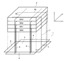
図1は、本発明の実施の形態に係る抵抗変化メモリ装置の基本構成、すなわち半導体基板1上のグローバルバス等の配線が形成される配線領域3とその上に積層されたメモリブロック2の構成を示している。
[First Embodiment]
FIG. 1 shows a basic configuration of a resistance change memory device according to an embodiment of the present invention, that is, a configuration of a
図1に示すように、メモリブロック2は、この例では4層のメモリセルアレイMA0〜MA3からなる。メモリブロック2の直下の半導体基板1には、配線領域3が設けられる。配線領域3には、メモリブロック2に書き込み/読み出しされるデータを外部とやり取りするためのグローバルバス等が設けられる。また、この配線領域3には後述するカラムスイッチ等を含むカラム制御回路や、ロウデコーダ等を含むロウ制御回路が設けられていてもよい。
As shown in FIG. 1, the
積層された各メモリセルアレイMAのワード線WL及びビット線BLと、半導体基板1上に形成された配線領域3とを接続するために、メモリブロック2の側面に垂直配線(ビアコンタクト)が必要になる。配線領域3の四辺には、ビット線コンタクト領域4及びワード線コンタクト領域5が設けられている。ビット線コンタクト領域4及びワード線コンタクト領域5には、ビット線BL及びワード線WLと制御回路とを接続するためのビット線コンタクト6及びワード線コンタクト7が形成される。ワード線WLは、その一端がワード線コンタクト領域5に形成されたワード線コンタクト7を介して配線領域3に接続されている。また、ビット線BLは、その一端がビット線コンタクト領域4に形成されたビット線コンタクト6を介して配線領域3に接続されている。
In order to connect the word line WL and the bit line BL of each stacked memory cell array MA and the
図1では、複数のメモリセルアレイMAを半導体基板1に垂直な方向(図1に示すz方向)に積層した1つのメモリブロック2について示しているが、実際にはこのような単位メモリブロック2がワード線WLの長手方向(図1に示すx方向)及びビット線BLの長手方向(図1に示すy方向)に複数個マトリクス状に配置される。
FIG. 1 shows one
図1に示すように、本実施の形態では、ワード線コンタクト領域5では、一列のコンタクトのみ、すなわち一断面での全ての層のワード線WLが共通コンタクトを介して配線領域3に接続されている。また、ビット線コンタクト領域4では、各層のビット線BLが別々に用意された4列のコンタクトを介して配線領域3に接続されている。本実施の形態では、ビット線BLは層毎に独立駆動され、ワード線WLは全ての層で共通に接続されているが、ワード線WLについても層毎に独立駆動するようにしても良い。また、ビット線BLを共通にして、ワード線WLを独立駆動するようにしても良い。更に、ビット線BL及びワード線WLの少なくとも一方を上下の層で共有するように構成することもできる。
As shown in FIG. 1, in the present embodiment, in the word
図2は、抵抗変化メモリ装置のメモリセルアレイMAの等価回路を示す回路図である。ここで、図2に示すメモリセルアレイMAは、ビット線BLの長手方向(図2に示すy方向)に例えば2Kbit(2048個)、ワード線WLの長手方向(図2に示すx方向)に例えば512bitの単位メモリセルMCが配置されている。これにより、1つのメモリセルアレイMA内に1Mbit(約106個)の単位メモリセルMCが配置される。1つのメモリセルアレイMA内では、単位メモリセルMCが二次元マトリクス状に配列されている。図示のようにワード線WLとビット線BLとの交差部に、整流素子例えばダイオードDiと可変抵抗素子VRとが直列接続された抵抗変化型の単位メモリセルMCが配置される。ここで、メモリセルMCを構成するダイオードDi及び可変抵抗素子VRの配置、極性も、図示のものに限定されない。 FIG. 2 is a circuit diagram showing an equivalent circuit of the memory cell array MA of the resistance change memory device. Here, the memory cell array MA shown in FIG. 2 has, for example, 2 Kbits (2048) in the longitudinal direction of the bit lines BL (y direction shown in FIG. 2) and, for example, in the longitudinal direction of the word lines WL (x direction shown in FIG. 2). A 512-bit unit memory cell MC is arranged. As a result, 1 Mbit (about 10 6 ) unit memory cells MC are arranged in one memory cell array MA. In one memory cell array MA, unit memory cells MC are arranged in a two-dimensional matrix. As shown in the figure, a resistance change type unit memory cell MC in which a rectifying element, for example, a diode Di and a variable resistance element VR are connected in series is arranged at an intersection of the word line WL and the bit line BL. Here, the arrangement and polarity of the diode Di and the variable resistance element VR constituting the memory cell MC are not limited to those shown in the drawing.
可変抵抗素子VRは例えば、電極/遷移金属酸化物/電極からなる構造を有するもの等であり、電圧、電流、熱等の印加条件により金属酸化物の抵抗値変化をもたらし、その抵抗値の異なる状態を情報として不揮発に記憶する。この可変抵抗素子VRとしては、より具体的には、カルコゲナイド等のように結晶状態と非晶質状態の相転移により抵抗値を変化させるもの(PCRAM)、金属陽イオンを析出させて電極間に架橋(コンタクティングブリッジ)を形成したり、析出した金属をイオン化して架橋を破壊したりすることで抵抗値を変化させるもの(CBRAM:Conductive Bridging RAM)、電圧あるいは電流印加により抵抗値が変化するもの(ReRAM)(電極界面に存在する電荷トラップにトラップされた電荷の存在の有無により抵抗変化が起きるものと、酸素欠損等に起因する伝導パスの存在の有無により抵抗変化が起きるものとに大別される。)等を用いることができる。 The variable resistance element VR has, for example, an electrode / transition metal oxide / electrode structure, etc., which causes a change in the resistance value of the metal oxide depending on application conditions such as voltage, current, and heat, and the resistance values thereof are different. The state is stored in a nonvolatile manner as information. More specifically, as the variable resistance element VR, a resistance value is changed by a phase transition between a crystalline state and an amorphous state, such as chalcogenide (PCRAM), a metal cation is deposited between the electrodes. The resistance value is changed by applying a voltage or current (CBRAM: Conductive Bridging RAM) that forms a bridge (contacting bridge) or ionizes the deposited metal to break the bridge. (ReRAM) (Resistivity changes depending on the presence or absence of charges trapped in charge traps existing at the electrode interface, and resistance changes depending on the presence or absence of conduction paths due to oxygen deficiency, etc. Etc.) and the like can be used.
ユニポーラ型のReRAMの場合、メモリセルMCに対するデータの書き込みは、可変抵抗素子VRに例えば3.5V(ダイオードDiの電圧降下分を含めると実際には4.5V程度)の電圧、10nA程度の電流を10ns−100ns程度の時間印加する。これにより、可変抵抗素子VRが高抵抗状態から低抵抗状態へと変化する。以下、この可変抵抗素子VRを高抵抗状態から低抵抗状態へ変化させる動作をセット動作という。 In the case of a unipolar type ReRAM, data is written to the memory cell MC by, for example, a voltage of 3.5 V (actually about 4.5 V including the voltage drop of the diode Di) in the variable resistance element VR and a current of about 10 nA. Is applied for a time of about 10 ns to 100 ns. As a result, the variable resistance element VR changes from the high resistance state to the low resistance state. Hereinafter, the operation of changing the variable resistance element VR from the high resistance state to the low resistance state is referred to as a set operation.
セット動作後の低抵抗状態の可変抵抗素子VRに対し、0.8V(ダイオードDiの電圧降下分を含めると実際には1.8V程度)の電圧、1μA−10μA程度の電流を500ns−2μs程度の時間印加する。これにより、可変抵抗素子VRが低抵抗状態から高抵抗状態へと変化する。以下、この可変抵抗素子VRを低抵抗状態から高抵抗状態へ変化させる動作をリセット動作という。 With respect to the variable resistance element VR in the low resistance state after the set operation, a voltage of 0.8 V (actually about 1.8 V including the voltage drop of the diode Di), a current of about 1 μA-10 μA is about 500 ns-2 μs. Apply for the time. Thereby, the variable resistance element VR changes from the low resistance state to the high resistance state. Hereinafter, the operation of changing the variable resistance element VR from the low resistance state to the high resistance state is referred to as a reset operation.
メモリセルMCは、例えば高抵抗状態を安定状態(リセット状態)とし、2値データ記憶であれば、リセット状態を低抵抗状態に変化させるセット動作によりデータの書き込みを行う。 For example, when the memory cell MC is in a stable state (reset state) in a high resistance state and binary data is stored, data is written by a set operation that changes the reset state to a low resistance state.
メモリセルMCのリード動作は、可変抵抗素子VRに0.4V(ダイオードDiの電圧降下分を含めると実際には1.4V程度)の電圧を与え、可変抵抗素子VRを介して流れる電流をモニターする。これにより、可変抵抗素子VRが低抵抗状態にあるか高抵抗状態にあるかを判定する。 In the read operation of the memory cell MC, a voltage of 0.4 V (actually about 1.4 V including the voltage drop of the diode Di) is applied to the variable resistance element VR, and the current flowing through the variable resistance element VR is monitored. To do. Thereby, it is determined whether the variable resistance element VR is in a low resistance state or a high resistance state.
図2には、メモリセルMCのセット動作時において、メモリセルアレイMAに接続されたビット線BL及びワード線WLに印加される電圧の状態が示されている。ここで、セット動作によりデータが書き込まれる選択メモリセルMCはMC11であるとして説明を行う。 FIG. 2 shows a state of voltages applied to the bit line BL and the word line WL connected to the memory cell array MA during the setting operation of the memory cell MC. Here, description will be made assuming that the selected memory cell MC into which data is written by the set operation is MC11.
選択メモリセルMC11に接続されていない非選択ビット線BL00、BL02、BL03は、“L”状態(本実施の形態ではフローティング状態≒0V)である。セット動作時において、選択メモリセルMC11に接続された選択ビット線BL01は、“L”状態(フローティング状態≒0V)から“H”状態(本実施の形態では電圧VSET)に駆動される。また、選択メモリセルMC11に接続されていない非選択ワード線WL00、WL02、WL03は、“H”状態(本実施の形態では電圧VSET)である。セット動作時において、選択メモリセルMC11に接続された選択ワード線WL01は、この“H”状態(電圧VSET)から“L”状態(本実施の形態では電圧Vss=0V)に駆動される。これにより、選択メモリセルMC11のダイオードDiが順方向バイアス状態となり電流が流れ、選択メモリセルMC11の可変抵抗素子VRが高抵抗状態から低抵抗状態へと変化し、セット動作が完了する。 The unselected bit lines BL00, BL02, BL03 that are not connected to the selected memory cell MC11 are in the “L” state (in the present embodiment, the floating state≈0 V). During the set operation, the selected bit line BL01 connected to the selected memory cell MC11 is driven from the “L” state (floating state≈0 V) to the “H” state (voltage VSET in this embodiment). In addition, unselected word lines WL00, WL02, WL03 that are not connected to the selected memory cell MC11 are in the “H” state (voltage VSET in the present embodiment). During the set operation, the selected word line WL01 connected to the selected memory cell MC11 is driven from the “H” state (voltage VSET) to the “L” state (voltage Vss = 0 V in this embodiment). As a result, the diode Di of the selected memory cell MC11 is in the forward bias state, current flows, the variable resistance element VR of the selected memory cell MC11 changes from the high resistance state to the low resistance state, and the set operation is completed.
本実施の形態において、非選択のメモリセルMCに接続された非選択のビット線BLには、セット動作時に電圧を印加せず、フローティング状態のままとしている。ビット線BLを制御するカラム制御回路は、セット動作時に特定のビット線BL(本実施の形態においてはビット線BL01)にセット電圧(本実施の形態においては電圧VSET)を印加する。しかし、カラム制御回路はセット動作時に選択されないその他の非選択ビット線BL(ビット線BL00、BL02、BL03)は制御する必要がない。そのため、非選択ビット線BL(ビット線BL00、BL02、BL03)を非選択状態(例えばVss=0V)に駆動する構成を省略することができる。すなわち、より簡易な構成のカラム制御回路でメモリセルアレイMAに対するセット動作を実行することができる。 In the present embodiment, no voltage is applied to the non-selected bit line BL connected to the non-selected memory cell MC during the set operation, and the floating state is maintained. The column control circuit that controls the bit line BL applies a set voltage (voltage VSET in this embodiment) to a specific bit line BL (bit line BL01 in the present embodiment) during the set operation. However, the column control circuit does not need to control other unselected bit lines BL (bit lines BL00, BL02, BL03) that are not selected during the set operation. Therefore, the configuration for driving the non-selected bit lines BL (bit lines BL00, BL02, BL03) to a non-selected state (for example, Vss = 0V) can be omitted. That is, the set operation for the memory cell array MA can be executed by a column control circuit having a simpler configuration.
[第2の実施の形態]
次に、本発明に係る抵抗変化メモリ装置の第2の実施の形態について図3〜図12を参照して説明する。図3は、抵抗変化メモリ装置のメモリセルアレイMAの配線を示す図である。また、図4は抵抗変化メモリ装置のカラム/ロウ制御回路の配置例を示すブロック図である。そして、図5〜図12は抵抗変化メモリ装置のカラム/ロウ制御回路の構成例を示す回路図である。ここで、第2の実施形態に係る抵抗変化メモリ装置の基本構成は、第1の実施形態に係る抵抗変化メモリ装置と同様である。第2の実施の形態に係る抵抗変化メモリ装置において、第1の実施の形態と同一の構成を有する箇所には、同一の符号を付すことによりその説明を省略する。
[Second Embodiment]
Next, a second embodiment of the resistance change memory device according to the present invention will be described with reference to FIGS. FIG. 3 is a diagram showing wiring of the memory cell array MA of the resistance change memory device. FIG. 4 is a block diagram showing an arrangement example of the column / row control circuit of the resistance change memory device. 5 to 12 are circuit diagrams showing configuration examples of the column / row control circuit of the resistance change memory device. Here, the basic configuration of the resistance change memory device according to the second embodiment is the same as that of the resistance change memory device according to the first embodiment. In the resistance change memory device according to the second embodiment, portions having the same configuration as in the first embodiment are denoted by the same reference numerals, and the description thereof is omitted.
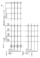
図3に示すように、本実施の形態に係るビット線BL及びワード線WLは階層化構造を有している。一群のビット線BLy<3:0>はビット線BLy0〜ビット線BLy3までの4本の配線からなる。また、一群のワード線WLx<7:0>はワード線WLx0〜ワード線WLx7までの8本の配線からなる。ここで、図3のメモリセルアレイMAの配線図においては、ビット線BL及びワード線WLの各交差部に配置されるメモリセルMCの記載を省略しているが、これは第1の実施形態と同様に各交差部に単位メモリセルMCが配置されているものとする。また、第1の実施の形態と同様に、セット動作時に選択されるビット線BL及びワード線WLは、ビット線BL01及びワード線WL01であるものとする。 As shown in FIG. 3, the bit line BL and the word line WL according to the present embodiment have a hierarchical structure. A group of bit lines BLy <3: 0> is composed of four wires from bit line BLy0 to bit line BLy3. A group of word lines WLx <7: 0> is composed of eight wires from word line WLx0 to word line WLx7. Here, in the wiring diagram of the memory cell array MA in FIG. 3, the description of the memory cells MC arranged at the intersections of the bit lines BL and the word lines WL is omitted, but this is the same as in the first embodiment. Similarly, it is assumed that unit memory cells MC are arranged at each intersection. Similarly to the first embodiment, the bit line BL and the word line WL selected during the set operation are the bit line BL01 and the word line WL01.
抵抗変化メモリ装置のセット動作時において、あるビット線群BLy<3:0>が後述するカラムデコーダにより選択される。本実施の形態においてはビット線群BL0<3:0>が選択されているものとする。選択されたビット線群BL0<3:0>のうち、選択メモリセルMCに接続されていない非選択ビット線BL00、BL02、BL03は、“L”状態(本実施の形態では0V)である。セット動作時に、選択されたビット線群BL0<3:0>のうち選択メモリセルMCに接続された選択ビット線BL01は、“L”状態(0V)から“H”状態(本実施の形態では電圧VSET)に駆動される。そして、選択されていない他のビット線群BLy<3:0>に含まれる全てのビット線BLy0〜BLy3はフローティング状態(≒0V)である。 During the setting operation of the resistance change memory device, a certain bit line group BLy <3: 0> is selected by a column decoder described later. In this embodiment, it is assumed that the bit line group BL0 <3: 0> is selected. Of the selected bit line group BL0 <3: 0>, the unselected bit lines BL00, BL02, BL03 not connected to the selected memory cell MC are in the “L” state (0 V in this embodiment). During the set operation, the selected bit line BL01 connected to the selected memory cell MC in the selected bit line group BL0 <3: 0> is changed from the “L” state (0V) to the “H” state (in this embodiment). Voltage VSET). All the bit lines BLy0 to BLy3 included in the other unselected bit line groups BLy <3: 0> are in the floating state (≈0 V).
また、抵抗変化メモリ装置のセット動作時には、ワード線群WLx<7:0>が後述するメインロウデコーダにより選択される。本実施の形態においてはワード線群WL0<7:0>が選択されているものとする。選択されたワード線群WL0<7:0>のうち、選択メモリセルMCに接続されていない非選択ワード線WL00、WL02、WL03等は、“H”状態(本実施の形態では電圧VSET)である。セット動作時に、選択されたワード線群WL0<7:0>のうち選択メモリセルMCに接続された選択ワード線WL01は、“H”状態(電圧VSET)から“L”状態(本実施の形態では電圧Vss=0V)に駆動される。そして選択されていない他のワード線群WLx<7:0>に含まれる全てのワード線WLx0〜WLx7は“H”状態(本実施の形態では電圧VSET)である。 Further, during the setting operation of the resistance change memory device, the word line group WLx <7: 0> is selected by a main row decoder described later. In the present embodiment, it is assumed that word line group WL0 <7: 0> is selected. Of the selected word line group WL0 <7: 0>, unselected word lines WL00, WL02, WL03, etc. that are not connected to the selected memory cell MC are in the “H” state (the voltage VSET in this embodiment). is there. During the set operation, the selected word line WL01 connected to the selected memory cell MC in the selected word line group WL0 <7: 0> changes from the “H” state (voltage VSET) to the “L” state (this embodiment). In this case, the voltage Vss is driven to 0V. All the word lines WLx0 to WLx7 included in other unselected word line groups WLx <7: 0> are in the “H” state (voltage VSET in this embodiment).
これにより、選択ビット線BL01及び選択ワード線WL01に接続された選択メモリセルMCのダイオードDiが順方向バイアス状態となり電流が流れ、選択メモリセルMCの可変抵抗素子VRが高抵抗状態から低抵抗状態へと変化し、セット動作が完了する。 As a result, the diode Di of the selected memory cell MC connected to the selected bit line BL01 and the selected word line WL01 enters a forward bias state, and current flows, and the variable resistance element VR of the selected memory cell MC changes from the high resistance state to the low resistance state. The setting operation is completed.
本実施の形態において、階層化構造を有するビット線BLのうち、選択メモリセルMCに接続された選択ビット線BL01を含まないビット線群BLy<3:0>には、セット動作時に電圧を印加せず、フローティング状態のままとしている。ビット線BLを制御するカラム制御回路は、セット動作時に選択ビット線BL(ビット線BL01)にセット電圧(電圧VSET)を印加する。また、非選択ビット線BL(BL00、BL02、BL03)には電圧Vssを印加している。しかし、カラム制御回路はセット動作時に選択されないビット線群BLy<3:0>は制御する必要がない。そのため、ビット線群BLy<3:0>を非選択状態(例えばVss=0V)に駆動する構成を省略して、より簡易な構成としたカラム制御回路でメモリセルアレイMAに対するセット動作を実行することができる。 In the present embodiment, a voltage is applied to the bit line group BLy <3: 0> that does not include the selected bit line BL01 connected to the selected memory cell MC among the bit lines BL having a hierarchical structure during the set operation. Without being left floating. The column control circuit that controls the bit line BL applies a set voltage (voltage VSET) to the selected bit line BL (bit line BL01) during the set operation. The voltage Vss is applied to the non-selected bit lines BL (BL00, BL02, BL03). However, the column control circuit does not need to control the bit line group BLy <3: 0> that is not selected during the set operation. Therefore, the configuration for driving the bit line group BLy <3: 0> to a non-selected state (for example, Vss = 0V) is omitted, and the set operation for the memory cell array MA is executed with a simpler column control circuit. Can do.
[制御回路の構成]
次に、ビット線BL及びワード線WLにこのような電圧を印加するためのカラム制御回路及びロウ制御回路の構成について説明する。ここでも、ワード線方向に2Kbit(=2048bit)、ビット線方向に512bitのメモリセルMCを配列して1MbitのメモリセルアレイMAを構成する場合を例として説明する。図4は、抵抗変化メモリ装置のカラム制御回路及びロウ制御回路の配置例を示すブロック図である。
[Configuration of control circuit]
Next, the configuration of the column control circuit and the row control circuit for applying such a voltage to the bit line BL and the word line WL will be described. Here, an example will be described in which a memory cell array MA of 1 Mbit is configured by arranging memory cells MC of 2 Kbit (= 2048 bits) in the word line direction and 512 bits in the bit line direction. FIG. 4 is a block diagram illustrating an arrangement example of the column control circuit and the row control circuit of the resistance change memory device.
図4に示されるように、ロウ制御回路は、例えばロウデコーダ10、メインロウデコーダ11、書き込み駆動線ドライバ12、ロウ電源線ドライバ13及びロウ系周辺回路14により構成される。また、カラム制御回路は、例えばカラムスイッチ20、カラムデコーダ21、センスアンプ/書き込みバッファ22、カラム電源線ドライバ23及びカラム系周辺回路24により構成される。
As shown in FIG. 4, the row control circuit includes, for example, a
本実施の形態に係るワード線WLは階層化構造を有しており、メインロウデコーダ11は、256対のメインワード線MWLx、MWLbx(x=<255:0>)のいずれか一対を選択駆動する。一例として、選択されたメインワード線MWLx、MWLbxでは、メインワード線MWLxが“H”状態となり、メインワード線MWLbxが“L”状態となる。逆に、非選択のメインワード線MWLx、MWLbxでは、メインワード線MWLxが“L”状態となり、メインワード線MWLbxが“H”状態となる。一対のメインワード線MWLx、MWLbxはひとつのロウデコーダ10に接続される。
The word lines WL according to the present embodiment have a hierarchical structure, and the
ロウデコーダ10は、メインワード線MWLx、MWLbxの階層下にある8本のワード線WLからなるワード線群WLx<7:0>のうちの1本を選択駆動する。メインロウデコーダ11により選択駆動されたメインワード線MWLx、MWLbxに接続されたロウデコーダ10が更にワード線WLを選択駆動することにより、1本のワード線WLが選択駆動される。書き込み駆動線ドライバ12には8本の書き込み駆動線WDRV<7:0>及びロウ電源線VRowが接続され、ロウ電源線ドライバ13にはロウ電源線VRowが接続されている。このロウ電源線VRowには、非選択のメインワード線MWL、MWLbxの階層下のワード線WL、及び選択されたメインワード線MWL、MWLbxの階層下の非選択のワード線WLに供給される電圧(VSET)が印加される。
The
書き込み駆動線WDRV<7:0>及びロウ電源線VRowはロウデコーダ10に接続される。書き込み駆動線WDRV<7:0>及びロウ電源線VRowには、ロウデコーダ10がワード線WLを駆動するための電圧が印加される。具体的には、セット動作時において8本の書き込み駆動線WDRV<7:0>のうち選択ワード線WLに対応する1本の書き込み駆動線WDRVに電圧Vss(=0V)を供給し、それ以外の7本には電圧VSETを供給する。ロウ系周辺回路14は、この抵抗変化メモリ装置全体の管理を行うもので、外部のホスト装置からの制御信号を受け付け、読み出し、書き込み、消去、データの入出力管理等を行う。
The write drive line WDRV <7: 0> and the row power supply line VRow are connected to the
本実施の形態に係るビット線BLも階層化構造を有しており、カラムデコーダ21は、128本のカラム選択線CSLy(y=<127:0>)のいずれか一本を選択駆動する。一例として、選択されたカラム選択線CSLyが“H”状態となる。逆に、非選択のカラム選択線CSLyが“L”状態となる。一本のカラム選択線CSLyはひとつのカラムスイッチ20に接続される。
The bit line BL according to the present embodiment also has a hierarchical structure, and the
カラムスイッチ20は、カラム選択線CSLyの階層下にある4本のビット線BLからなるビット線群BLy<3:0>のうちの1本を選択駆動する。カラムデコーダ21により選択駆動されたカラム選択線CSLyに接続されたカラムスイッチ20が更にビット線BLを選択駆動することにより、1本のビット線BLが選択駆動される。センスアンプ/書き込みバッファ22は、ローカルデータ線LDQ<3:0>に読み出された信号を検知増幅するとともに、データ入出力線IO<3:0>から入力される書き込みデータをカラムスイッチ20を介してメモリセルMCに供給するものである。センスアンプ/書き込みバッファ22には、4本のローカルデータ線LDQ<3:0>及びカラム電源線VCol1が接続され、カラム電源線ドライバ23にはカラム電源線VCol1が接続されている。
The
ローカルデータ線LDQ<3:0>はカラムスイッチ20に接続され、カラムスイッチ20がビット線BLを駆動するための電圧が印加される。具体的には、セット動作時において4本のローカルデータ線LDQ<3:0>のうち選択ビット線BLに対応する1本のローカルデータ線LDQに電圧VSETを供給し、それ以外の3本には電圧Vss=0Vを供給する。また、セット動作時において、カラム選択線CSLyにより選択されなかったカラムスイッチ20は、ビット線駆動動作を実行せず、ビット線群BLy<3:0>をフローティング状態にする。カラム系周辺回路24は、この抵抗変化メモリ装置全体の管理を行うもので、外部のホスト装置からの制御信号を受け付け、読み出し、書き込み、消去、データの入出力管理等を行う。
The local data lines LDQ <3: 0> are connected to the
次に、図5〜図8を参照して、ロウ制御回路の構成を詳細に説明する。図5〜図8は抵抗変化メモリ装置のロウ制御回路の構成例を示す回路図である。 Next, the configuration of the row control circuit will be described in detail with reference to FIGS. 5 to 8 are circuit diagrams showing configuration examples of the row control circuit of the resistance change memory device.
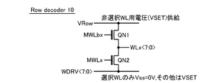
[ロウデコーダ10の構成]
図4及び図5に示されるように、ロウデコーダ10には256対のメインワード線MWLx及びMWLbx(x=<255:0>)のいずれか一対、ロウ電源線VRow並びに書き込み駆動線WDRV<7:0>が接続されている。また、ロウデコーダ10には、ワード線群WLx<7:0>が接続されており、このワード線群WLx<7:0>は一列に並んで設けられた複数のメモリセルMCに接続されている。前述のように1つのロウデコーダ10に接続されるワード線群WLx<7:0>はワード線WLx0〜ワード線WLx7までの8本の配線からなる。同様に、書き込み駆動線WDRV<7:0>は、WDRV0〜WDRV7までの8本の配線からなる配線である。
[Configuration of Row Decoder 10]
4 and 5, the
図5に示すように、ロウデコーダ10は、2つのNMOSトランジスタQN1及びQN2のソースを互いに接続してなるトランジスタ対を8つ備えて構成されている。トランジスタQN1のゲートにメインワード線MWLbxが、ドレインにロウ電源線VRowが接続されている。また、トランジスタQN2のゲートにメインワード線MWLxが、ドレインに書き込み駆動線WDRV<7:0>のいずれか1本が接続されている。そして、トランジスタQN1及びQN2のソースはともにワード線群WLx<7:0>のいずれか1本に接続されている。
As shown in FIG. 5, the
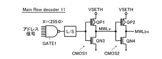
[メインロウデコーダ11の構成]
図4及び図6に示されるように、メインロウデコーダ11には256対のメインワード線MWLx及びMWLbx(x=<255:0>)、並びにアドレス信号線が接続されている。本実施の形態に係る抵抗変化メモリ装置のワード線WLは階層化構造を有している。メインロウデコーダ11はプリデコーダであり、一組のメインワード線MWLx、MWLbxは1つのロウデコーダ10内の8つのトランジスタ対(図5のQN1、QN2)にそれぞれ接続され、1つのロウデコーダ10は8本のワード線WLx<7:0>のいずれか1本を選択することができる。メインロウデコーダ11は、図6に示すような回路を、1対のメインワード線MWLx、MWLbxごとに有している。
[Configuration of Main Row Decoder 11]
As shown in FIGS. 4 and 6, the
図6に示すように、1つのメインロウデコーダ11において、メインロウデコーダ11に接続されたアドレス信号線は、論理ゲートGATE1に接続される。論理ゲートGATE1の出力信号はレベルシフタL/Sを介してPMOSトランジスタQP1及びNMOSトランジスタQN3からなるCMOSインバータCMOS1の入力端子に供給される。トランジスタQP1のソースに電源VSETHが接続され、トランジスタQN3のソースは接地されている。そして、トランジスタQP1及びQN3のドレインはともにメインワード線MWLxに接続される。
As shown in FIG. 6, in one
また、メインワード線MWLxは、PMOSトランジスタQP2及びNMOSトランジスタQN4からなるCMOSインバータCMOS2に接続されている。トランジスタQP2のソースにも電源VSETHが接続され、トランジスタQN4のソースは接地されている。そして、トランジスタQP2及びQN4のドレインはともにメインワード線MWLbxに接続される。 The main word line MWLx is connected to a CMOS inverter CMOS2 including a PMOS transistor QP2 and an NMOS transistor QN4. The power source VSETH is also connected to the source of the transistor QP2, and the source of the transistor QN4 is grounded. The drains of the transistors QP2 and QN4 are both connected to the main word line MWLbx.
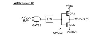
[書き込み駆動線ドライバ12の構成]
図4及び図7に示されるように、書き込み駆動線ドライバ12には、ロウ電源線VRow及びアドレス信号線が接続されている。ここで、書き込み駆動線ドライバ12も、プリデコーダである。
[Configuration of Write Drive Line Driver 12]
As shown in FIGS. 4 and 7, the row power supply line VRow and the address signal line are connected to the write
書き込み駆動線ドライバ12に接続されたアドレス信号線は、論理ゲートGATE2に接続される。論理ゲートGATE2の出力信号はレベルシフタL/Sを介してPMOSトランジスタQP3及びNMOSトランジスタQN5からなるCMOSインバータCMOS3の入力端子に供給される。トランジスタQP3のソースには、後述するように電圧VSETが印加されているロウ電源線VRowが接続され、トランジスタQN5のソースは接地されている。そして、トランジスタQP3及びQN5のドレインはともに書き込み駆動線WDRV<7:0>に接続される。
The address signal line connected to the write
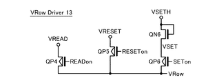
[ロウ電源線ドライバ13の構成]
図4及び図8に示されるように、ロウ電源線ドライバ13には、ロウ電源線VRow及び制御信号線が接続されている。ロウ電源線ドライバ13において、電源VREADがPMOSトランジスタQP4を介して、電源VRESETがPMOSトランジスタQP5を介してそれぞれロウ電源線VRowに接続されている。トランジスタQP4のゲートには制御信号READonが供給され、トランジスタQP5のゲートには制御信号RESETonが供給される。制御信号READon、RESETonは、それぞれデータ読み出し時、リセット動作時に“H”状態から“L”状態となる。
[Configuration of Row Power Line Driver 13]
As shown in FIGS. 4 and 8, the row power
また、ロウ電源線ドライバ13には、電源VSETHが接続されている。電源VSETHはNMOSトランジスタQN6のドレイン及びゲートに接続される。トランジスタQN6のソースがPMOSトランジスタQP6を介してロウ電源線VRowに接続されている。トランジスタQP6のゲートには制御信号SETonが供給される。
Further, a power supply VSETH is connected to the row power
次に、図9〜図12を参照して、カラム制御回路の構成を詳細に説明する。図9〜図12は抵抗変化メモリ装置のカラム制御回路の構成例を示す回路図である。 Next, the configuration of the column control circuit will be described in detail with reference to FIGS. 9 to 12 are circuit diagrams showing configuration examples of the column control circuit of the resistance change memory device.
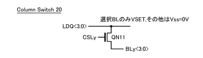
[カラムスイッチ20の構成]
図4及び図9に示されるように、カラムスイッチ20には128本のカラム選択線CSLy(y=<127:0>)のいずれか一本及びローカルデータ線LDQ<3:0>が接続されている。また、カラムスイッチ20には、ビット線群BLy<3:0>が接続されており、このビット線BLは一列に並んで設けられた複数のメモリセルMCに接続されている。前述のように、1つのカラムスイッチ20に接続されるビット線群BLy<3:0>はビット線BLy0〜ビット線BLy3までの4本の配線からなる。同様に、ローカルデータ線LDQ<3:0>は、LDQ0〜LDQ3までの4本の配線からなる配線である。
[Configuration of column switch 20]
As shown in FIGS. 4 and 9, one of 128 column selection lines CSLy (y = <127: 0>) and the local data line LDQ <3: 0> are connected to the
図9に示すように、カラムスイッチ20は、1つのNMOSトランジスタQN11から構成され、1つのカラムスイッチ20は、このトランジスタQN11からなる構成を4つ備える。トランジスタQN11のゲートにカラム選択線CSLyが、ドレインにローカルデータ線LDQ<3:0>のいずれか1本が接続されている。そして、トランジスタQN11のソースはビット線群BLy<3:0>のいずれか1本に接続されている。
As shown in FIG. 9, the
[カラムデコーダ21の構成]
図4及び図10に示されるように、カラムデコーダ21には128本のカラム選択線CSLy(y=<127:0>)及びアドレス信号線が接続されている。本実施の形態に係る抵抗変化メモリ装置において、一本のカラム選択線CSLyは1つのカラムスイッチ20内の4つのトランジスタ(図9のQN11)にそれぞれ接続され、1つのカラムスイッチ20は4本のビット線群BLy<3:0>のいずれか1本を選択することができる。カラムデコーダ21は、図10に示すような回路を、一本のカラム選択線CSLy毎に有している。
[Configuration of the column decoder 21]
As shown in FIGS. 4 and 10, the
図10に示すように、1つのカラムデコーダ21において、カラムデコーダ21に接続されたアドレス信号線は、論理ゲートGATE3に接続される。論理ゲートGATE3の出力信号はレベルシフタL/Sを介してPMOSトランジスタQP11及びNMOSトランジスタQN13からなるCMOSインバータCMOS11の入力端子に供給される。トランジスタQP11のソースに電源VSETHが接続され、トランジスタQN13のソースは接地されている。そして、トランジスタQP11及びQN13のドレインはともにカラム選択線CSLyに接続されている。
As shown in FIG. 10, in one
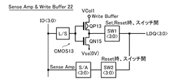
[センスアンプ/書き込みバッファ22の構成]
図4及び図11に示されるように、センスアンプ/書き込みバッファ22には、カラム電源線VCol1、ローカルデータ線LDQ<3:0>及びデータ入出力線IO<3:0>が接続されている。まず、書き込みバッファ部分について、その構成を説明する。センスアンプ/書き込みバッファ22に接続されたデータ入出力線IO<3:0>は、レベルシフタL/Sを介してPMOSトランジスタQP13及びNMOSトランジスタQN15からなるCMOSインバータCMOS13に接続される。トランジスタQP13のソースにはカラム電源線VCol1が接続されている。カラム電源線VCol1には後述するように電圧VSETが印加されている。また、トランジスタQN15のソースは接地されている。そして、トランジスタQP13及びQN15のドレインはともにスイッチSW1を介してローカルデータ線LDQ<3:0>に接続されている。
[Configuration of Sense Amplifier / Write Buffer 22]
As shown in FIGS. 4 and 11, to the sense amplifier /
次にセンスアンプ部分について、その構成を説明する。センスアンプ/書き込みバッファ22に接続されたデータ入出力線IO<3:0>は、センスアンプS/Aに接続される。センスアンプS/Aとしては、シングルエンド型、参照セルを用いた差動型等、種々のタイプを用いるとこができる。センスアンプS/Aの出力端子はスイッチSW2を介してローカルデータ線LDQ<3:0>に接続されている。
Next, the configuration of the sense amplifier portion will be described. The data input / output lines IO <3: 0> connected to the sense amplifier /
[カラム電源線ドライバ23の構成]
図4及び図12に示されるように、カラム電源線ドライバ23には、カラム電源線VCol1及び制御信号線が接続されている。カラム電源線ドライバ23において、電源VRESETがPMOSトランジスタQP15を介してカラム電源線VCol1に接続されている。トランジスタQP15のゲートには制御信号RESETonが供給される。また、電源VSETHがNMOSトランジスタQN16のドレイン及びゲートに接続され、トランジスタQN16のソースはPMOSトランジスタQP14を介してカラム電源線VCol1に接続されている。トランジスタQP14のゲートには制御信号SETonが供給される。
[Configuration of Column Power Line Driver 23]
As shown in FIGS. 4 and 12, the column power
次に、このように構成された抵抗変化メモリ装置のセット動作について説明する。まず、セット動作時における抵抗変化メモリ装置のロウ制御回路の動作について、図4〜図8を参照して説明する。図4に示すようにワード線WLは階層化構造を有している。メインロウデコーダ11及びロウデコーダ10により選択駆動されるワード線群WLx<7:0>には、書き込み駆動線WDRV<7:0>又はロウ電源線VRowに印加されている電圧が印加される。まず、ロウデコーダ10に接続された書き込み駆動線WDRV<7:0>及びロウ電源線VRowに対する電圧の印加動作について説明する。
Next, a setting operation of the resistance change memory device configured as described above will be described. First, the operation of the row control circuit of the resistance change memory device during the set operation will be described with reference to FIGS. As shown in FIG. 4, the word line WL has a hierarchical structure. A voltage applied to the write drive line WDRV <7: 0> or the row power supply line VRow is applied to the word line group WLx <7: 0> that is selectively driven by the
[ロウ電源線ドライバ13の動作]
セット動作時には、ロウ電源線ドライバ13において、トランジスタQP6のゲートに供給されていた制御信号(SETon信号)が“L”状態になり導通する。電源VSETHの電圧VSETHはNMOSトランジスタQN6により転送されて電圧VSETとなる。セット動作時に、ロウ電源線ドライバ13はロウ電源線VRowを電圧VSETに駆動する。
[Operation of Row Power Line Driver 13]
At the time of the set operation, in the row power
[書き込み駆動線ドライバ12の動作]
書き込み駆動線ドライバ12の論理ゲートGATE2には、アドレス信号が入力される。このアドレス信号に基づき、論理ゲートGATE2は、アドレス信号に対応する一の書き込み駆動線(例えばWDRV1)について、“H”信号を、対応しない他の書き込み駆動線について“L”信号をCMOSインバータCMOS3の入力端子に供給する。アドレス信号に対応する書き込み駆動線(例えばWDRV1)の場合、CMOSインバータCMOS3の入力端子には“H”信号が供給され、導通したトランジスタQN5を介して接地電圧Vss(例えば0V)が書き込み駆動線WDRV1に印加される。アドレス信号に対応しない書き込み駆動線の場合、CMOSインバータCMOS3の入力端子には“L”信号が供給され、導通したトランジスタQP3を介してロウ電源線VRowの電圧(VSET)が書き込み駆動線WDRVに印加される。
[Operation of Write Drive Line Driver 12]
An address signal is input to the
次に、メインロウデコーダ11及びロウデコーダ10によるメインワード線MWLx、MWLbxとワード線WLx<7:0>の選択駆動動作について説明する。
Next, the selection drive operation of the main word lines MWLx and MWLbx and the word lines WLx <7: 0> by the
[メインロウデコーダ11の動作]
メインロウデコーダ11の論理ゲートGATE1の入力端子にも、アドレス信号が供給される。このアドレス信号に基づき、論理ゲートGATE1は、x=<255:0>のうち選択されたx(例えばx=0)について“L”信号を、選択されていないxについて“H”信号をCMOSインバータCMOS1の入力端子に供給する。まず、選択されたx(例えばx=0)について説明する。選択されたx(例えばx=0)の場合、CMOSインバータCMOS1の入力端子には“L”信号が供給され、導通したトランジスタQP1を介して電源VSETHの“H”信号がメインワード線MWL0に供給される。また、メインワード線MWL0の“H”信号は、CMOSインバータCMOS2の入力端子に供給され、導通したトランジスタQN4を介して接地電圧Vssの“L”信号がメインワード線MWLb0に供給される。すなわち、選択されたx(例えばx=0)の場合、メインワード線MWL0には、“H”信号、メインワード線MWLb0には“L”信号が供給される。
[Operation of Main Row Decoder 11]
An address signal is also supplied to the input terminal of the
次に、選択されていないxについて説明する。選択されていないxの場合、CMOSインバータCMOS1の入力端子には“H”信号が供給され、導通したトランジスタQN3を介して接地電圧Vssの“L”信号がメインワード線MWLxに供給される。また、メインワード線MWLxの“L”信号は、CMOSインバータCMOS2の入力端子に供給され、導通したトランジスタQP2を介して電源VSETHの“H”信号がメインワード線MWLbxに供給される。すなわち、選択されていないxの場合、メインワード線MWLxには、“L”信号、メインワード線MWLbxには“H”信号が供給される。 Next, x that has not been selected will be described. In the case of x that is not selected, the “H” signal is supplied to the input terminal of the CMOS inverter CMOS1, and the “L” signal of the ground voltage Vss is supplied to the main word line MWLx via the transistor QN3 that has become conductive. Further, the “L” signal of the main word line MWLx is supplied to the input terminal of the CMOS inverter CMOS2, and the “H” signal of the power supply VSETH is supplied to the main word line MWLbx via the transistor QP2 that has become conductive. That is, in the case of x that is not selected, the “L” signal is supplied to the main word line MWLx, and the “H” signal is supplied to the main word line MWLbx.
[ロウデコーダ10の動作]
ロウデコーダ10は、メインワード線MWLx及びMWLbxに供給された信号に基づき、ロウ電源線VRow又は書き込み駆動線WDRVの電圧をワード線WLに対して印加する。選択されたx(例えばx=0)の場合、メインワード線MWL0には、“H”信号、メインワード線MWLb0には“L”信号が供給されている。ロウデコーダ10のトランジスタQN1のゲートに“L”信号が供給され、トランジスタQN2のゲートに“H”信号が供給されるため、ワード線群WL0<7:0>には導通したトランジスタQN2を介して書き込み駆動線WDRV<7:0>の電圧が印加される。ここで、アドレス信号に対応する書き込み駆動線(例えばWDRV1)には、接地電圧(例えば0V)が印加され、アドレス信号に対応しないその他の書き込み駆動線には、ロウ電源線VRowの電圧(例えばVSET)が印加されている。ワード線群WL0<7:0>のうち、アドレス信号に対応するワード線WL01の1本のみに接地電圧(例えば0V)が印加され、その他のワード線WLには電圧VSETが印加される。
[Operation of Row Decoder 10]
The
また、選択されていないxの場合、メインワード線MWLxには、“L”信号、メインワード線MWLbxには“H”信号が供給されている。ロウデコーダ10のトランジスタQN1のゲートに“H”信号が供給され、トランジスタQN2のゲートに“L”信号が供給されるため、ワード群線WLx<7:0>には導通したトランジスタQN1を介してロウ電源線VRowの電圧(VSET)が印加される。これにより、セット動作時にはアドレス信号により選択された1本のワード線WL01のみに接地電圧(0V)が印加され、その他の全てのワード線WLにはロウ電源線VRowの電圧(VSET)が印加される。
In the case of x not selected, an “L” signal is supplied to the main word line MWLx, and an “H” signal is supplied to the main word line MWLbx. Since the “H” signal is supplied to the gate of the transistor QN1 of the
次に、セット動作時における抵抗変化メモリ装置のカラム制御回路の動作について、図4及び図9〜図12を参照して説明する。カラムデコーダ21及びカラムスイッチ20により選択駆動されるビット線群BLy<3:0>には、ローカルデータ線LDQ<3:0>に印加されている電圧が印加される。まず、カラムスイッチ20に接続されたローカルデータ線LDQ<3:0>及びカラム電源線VCol1に対する電圧の印加動作について説明する。
Next, the operation of the column control circuit of the resistance change memory device during the set operation will be described with reference to FIGS. 4 and 9 to 12. The voltage applied to the local data lines LDQ <3: 0> is applied to the bit line group BLy <3: 0> that is selectively driven by the
[カラム電源線ドライバ23の動作]
セット動作時には、カラム電源線ドライバ23において、トランジスタQP14のゲートに供給されていた制御信号(SETon信号)が“L”状態になり導通する。電源VSETHの電圧VSETHはNMOSトランジスタQN16により転送されて電圧VSETとなり、電圧VSETでカラム電源線VCol1を駆動する。
[Operation of the column power line driver 23]
At the time of the set operation, in the column
[センスアンプ/書き込みバッファ22の動作]
センスアンプ/書き込みバッファ22において、セット動作時に書き込みバッファ部のスイッチSW1がオンとなり導通状態になるとともに、センスアンプ部のスイッチSW2がオフとなり非導通状態になる。センスアンプ/書き込みバッファ22には、データ入出力線IO<3:0>より書き込みデータが供給される。この書き込みデータがレベルシフタL/Sを介してCMOSインバータCMOS13の入力端子に供給される。このデータに応じてローカルデータ線LDQ<3:0>には電圧VSET又は接地電圧(Vss=0V)が印加される。
[Operation of Sense Amplifier / Write Buffer 22]
In the sense amplifier /
次に、カラムデコーダ21及びカラムスイッチ20によるカラム選択線CSLyとビット線群BLy<3:0>の選択駆動動作について説明する。
Next, the selection driving operation of the column selection line CSLy and the bit line group BLy <3: 0> by the
[カラムデコーダ21の動作]
カラムデコーダ21の論理ゲートGATE3の入力端子には、アドレス信号が供給される。このアドレス信号に基づき、論理ゲートGATE3は、y=<127:0>のうち選択されたy(例えばy=0)について“L”信号を、選択されていないyについて“H”信号をCMOSインバータCMOS11の入力端子に供給する。まず、選択されたy(例えばy=0)について説明する。選択されたy(例えばy=0)の場合、CMOSインバータCMOS11の入力端子には“L”信号が供給され、導通したトランジスタQP11を介して電源VSETHの“H”信号がカラム選択線CSL0に供給される。次に、選択されていないyについて説明する。選択されていないyの場合、CMOSインバータCMOS11の入力端子には“H”信号が供給され、導通したトランジスタQN13を介して接地電圧Vssの“L”信号がカラム選択線CSLyに供給される。
[Operation of the column decoder 21]
An address signal is supplied to the input terminal of the
[カラムスイッチ20の動作]
カラムスイッチ20は、カラム選択線CSLyに供給された信号に基づき、ローカルデータ線LDQの電圧をビット線BLに対して印加する。選択されたy(例えばy=0)の場合、カラム選択線CSL0には、“H”信号が供給されている。カラムスイッチ20のトランジスタQN11のゲートに“H”信号が供給されるため、ビット線群BL0<3:0>には導通したトランジスタQN12を介してローカルデータ線LDQ<3:0>の電圧が印加される。ここで、アドレス信号に対応するローカルデータ線(例えばLDQ1)には、カラム電源線VCol1の電圧(VSET)が印加され、アドレス信号に対応しないその他のローカルデータ線には、接地電圧Vss(=0V)が印加されている。ビット線群BL0<3:0>のうち、アドレス信号に対応するビット線BL01の1本のみにカラム電源線VCol1の電圧(VSET)が印加され、その他のビット線BLには接地電圧Vss(=0V)が印加される。
[Operation of column switch 20]
The
一方、選択されていないyの場合、カラム選択線CSLyには、“L”信号が供給されている。カラムスイッチ20のトランジスタQN11のゲートに“L”信号が供給されるため導通せず、ビット線群BLy<3:0>には電圧が印加されない。そのため、ビット線群BLy<3:0>はフローティング状態になる。これにより、セット動作時には、アドレス信号により選択された1本のビット線BL01に電圧VSETが、非選択ビット線BLに接地電圧Vssが印加されるとともに、その他のビット線群BLy<3:0>はフローティング状態にされる。
On the other hand, when y is not selected, an “L” signal is supplied to the column selection line CSLy. Since the “L” signal is supplied to the gate of the transistor QN11 of the
このように、本実施の形態のカラム制御回路によれば、セット動作時にアドレス信号により選択された1本のビット線BL01のみにカラム電源線VCol1の電圧(VSET)が印加される。また、非選択のビット線BL00、BL02、BL03には接地電圧Vssが印加される。そして、その他のビット線群BLy<3:0>はフローティング状態にされる。 Thus, according to the column control circuit of the present embodiment, the voltage (VSET) of the column power supply line VCol1 is applied only to one bit line BL01 selected by the address signal during the set operation. The ground voltage Vss is applied to the non-selected bit lines BL00, BL02, BL03. The other bit line groups BLy <3: 0> are brought into a floating state.
本実施の形態において、階層化構造を有するビット線群BLy<3:0>のうち、選択メモリセルMCに接続された選択ビット線BL01を含まないビット線群BLy<3:0>には、セット動作時に電圧を印加せず、フローティング状態のままとしている。カラム制御回路はセット動作時に選択されないビット線群BLy<3:0>は制御する必要がない。そのため、ビット線群BLy<3:0>を非選択状態(例えばVss=0V)に駆動する構成を省略して、より簡易な構成としたカラム制御回路でメモリセルアレイMAに対するセット動作を実行することができる。 In the present embodiment, among the bit line groups BLy <3: 0> having a hierarchical structure, the bit line group BLy <3: 0> that does not include the selected bit line BL01 connected to the selected memory cell MC includes No voltage is applied during the set operation, and the floating state is maintained. The column control circuit does not need to control the bit line group BLy <3: 0> that is not selected during the set operation. Therefore, the configuration for driving the bit line group BLy <3: 0> to a non-selected state (for example, Vss = 0V) is omitted, and the set operation for the memory cell array MA is executed with a simpler column control circuit. Can do.
具体的には、カラムスイッチ20の構成を1つのトランジスタQN11からなる構成とすることができる。この構成によれば、カラム選択線CSLyにより選択されたカラムスイッチ20は、ビット線群BL0<3:0>を駆動させることができる。これとともに、カラム選択線CSLyにより選択されていないカラムスイッチ20は、ビット線群BLy<3:0>をフローティング状態に保つことが可能となる。特許文献2に記載された配線駆動回路のように、トランジスタを2つ直列接続し、これを切り替えることにより配線に駆動電圧又は接地電圧のいずれかを印加する構成とする必要がない。本実施の形態のカラムスイッチ20によれば、トランジスタの数を低減することができる。本実施の形態では、ワード線方向に2Kbit、ビット線方向に512bitのメモリセルMCを配列して1MbitのメモリセルアレイMAを構成している。カラムスイッチ20はカラム制御回路内にビット線BLの本数と同数(本実施の形態においては512個)設けられる。そのため、カラムスイッチ20内のトランジスタを削減することにより、カラム制御回路をより簡易な構成とすることができる。
Specifically, the configuration of the
[第3の実施の形態]
次に、本発明に係る抵抗変化メモリ装置の第3の実施の形態について図13を参照して説明する。図13は、抵抗変化メモリ装置のカラム/ロウ制御回路の動作タイミングを示すタイミングチャートである。ここで、第3の実施形態に係る抵抗変化メモリ装置の制御回路の構成は第1及び第2の実施形態に係る抵抗変化メモリ装置と同様である。第3の実施の形態に係る抵抗変化メモリ装置において、第1及び第2の実施の形態と同一の構成を有する箇所には、同一の符号を付すことによりその説明を省略する。本実施の形態に係る抵抗変化メモリ装置は、セット動作を実行する際にワード線WL及びビット線BLに電圧を印加するタイミングを異ならせる点において、第1及び第2の実施の形態と異なる。
[Third Embodiment]
Next, a third embodiment of the resistance change memory device according to the present invention will be described with reference to FIG. FIG. 13 is a timing chart showing the operation timing of the column / row control circuit of the resistance change memory device. Here, the configuration of the control circuit of the resistance change memory device according to the third embodiment is the same as that of the resistance change memory device according to the first and second embodiments. In the resistance change memory device according to the third embodiment, portions having the same configurations as those of the first and second embodiments are denoted by the same reference numerals, and the description thereof is omitted. The resistance change memory device according to the present embodiment is different from the first and second embodiments in that the timing of applying a voltage to the word line WL and the bit line BL is different when executing the set operation.
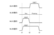
図13に示すように、選択メモリセルMCにセット動作を実行する場合に、まず、選択ワード線WL01及び非選択ワード線WLを含む全てのワード線WLに対して電圧VSETを印加する(時間t1)。ここで、全てのワード線WLに電圧VSETを印加する間、選択ビット線BL01及び非選択ビット線BLは、接地電圧Vssに保持されている。その後、選択メモリセルMCに接続された選択ワード線WL01のみに接地電圧Vssを印加する(時間t2)。時間t2において、選択ワード線WL01が電位Vssに下がった後、選択ビット線BL01に電圧VSETを印加するとともに、非選択ビット線BLをフローティング状態(≒0V)にする。 As shown in FIG. 13, when the set operation is performed on the selected memory cell MC, first, the voltage VSET is applied to all the word lines WL including the selected word line WL01 and the unselected word line WL (time t1). ). Here, while the voltage VSET is applied to all the word lines WL, the selected bit line BL01 and the non-selected bit line BL are held at the ground voltage Vss. Thereafter, the ground voltage Vss is applied only to the selected word line WL01 connected to the selected memory cell MC (time t2). At time t2, after the selected word line WL01 falls to the potential Vss, the voltage VSET is applied to the selected bit line BL01, and the non-selected bit line BL is set in a floating state (≈0V).
この結果、選択ビット線BL01と選択ワード線WL01とに接続された選択メモリセルMCのダイオードDiが順方向バイアス状態となり電流が流れ、選択メモリセルMCの可変抵抗素子VRが高抵抗状態から低抵抗状態へと変化し、セット動作が完了する。一方、選択ビット線BL01と非選択ワード線WLとに接続された非選択メモリセルMCの両端には共に電圧VSETが印加されるので、電流は流れない。また、非選択ビット線BLと選択ワード線WL01とに接続された非選択メモリセルMCの両端には0Vが印加されるため、こちらも電流が流れない。その後、時間t3において選択ビット線BL01及び非選択ワード線WLを電位Vssまで下げてセット動作を終了する。 As a result, the diode Di of the selected memory cell MC connected to the selected bit line BL01 and the selected word line WL01 is in a forward bias state and current flows, and the variable resistance element VR of the selected memory cell MC changes from the high resistance state to the low resistance state. It changes to the state and the set operation is completed. On the other hand, since the voltage VSET is applied to both ends of the non-selected memory cell MC connected to the selected bit line BL01 and the non-selected word line WL, no current flows. Further, since 0 V is applied to both ends of the non-selected memory cell MC connected to the non-selected bit line BL and the selected word line WL01, no current flows here either. Thereafter, at time t3, the selected bit line BL01 and the unselected word line WL are lowered to the potential Vss, and the set operation is completed.
ここで、図13に示す時間t1から時間t2の間、選択ビット線BL01及び非選択ビット線BLを電位Vssに保持するためには、図11に示す書き込みバッファ22においてローカルデータ線LDQ<3:0>を全て接地電圧Vssにする。これとともに、図10に示すカラムデコーダ21においてカラム選択線CSLyを全て“H”状態にする。これにより、図9に示す全てのカラムスイッチ20において、NMOSトランジスタQN11が導通し、ビット線群BLy<3:0>に、ローカルデータ線LDQ<3:0>の接地電圧Vssが印加される。このようにして、図13に示す時間t1から時間t2の間、選択ビット線BL01及び非選択ビット線BLの双方を電位Vssに保持することができる。
Here, in order to hold the selected bit line BL01 and the non-selected bit line BL at the potential Vss from the time t1 to the time t2 shown in FIG. 13, the local data line LDQ <3: in the
第2の実施の形態におけるセット動作の際、非選択のビット線BLをフローティング状態として、非選択のワード線WLに電圧VSETを印加すると、カップリングによりフローティング状態の非選択ビット線BLの電位が上昇する場合がある。この場合、非選択ビット線BLに接続された非選択メモリセルMCに対し、誤ってセット動作が実行されてしまうおそれがある。 During the set operation in the second embodiment, when the unselected bit line BL is in a floating state and the voltage VSET is applied to the unselected word line WL, the potential of the unselected bit line BL in the floating state is coupled due to coupling. May rise. In this case, there is a possibility that the set operation is erroneously performed on the non-selected memory cell MC connected to the non-selected bit line BL.
しかし、本実施の形態における抵抗変化メモリ装置においては、ワード線WL及びビット線BLに電圧を印加するタイミングをずらしている。そのため、ワード線WLを電圧VSETに立ち上げている間は、非選択ビット線BLは接地電圧Vssに保持されている。その後、セット動作時に非選択ビット線BLをフローティング状態としても、非選択ビット線BLの電位は接地電圧Vssからほとんど上がることがない。本実施の形態における抵抗変化メモリ装置によれば、非選択メモリセルMCに対して誤ってセット動作が実行されることがない。 However, in the resistance change memory device according to the present embodiment, the timing for applying the voltage to the word line WL and the bit line BL is shifted. Therefore, while the word line WL is raised to the voltage VSET, the unselected bit line BL is held at the ground voltage Vss. Thereafter, even if the non-selected bit line BL is in a floating state during the set operation, the potential of the non-selected bit line BL hardly rises from the ground voltage Vss. According to the resistance change memory device in the present embodiment, the set operation is not erroneously performed on the unselected memory cells MC.
本実施の形態に係る抵抗変化メモリ装置も、カラムスイッチ20の構成を1つのトランジスタQN11からなる構成とすることができる。この構成によれば、カラム選択線CSLyにより選択されたカラムスイッチ20は、ビット線群BL0<3:0>を駆動させることができる。これとともに、カラム選択線CSLyにより選択されていないカラムスイッチ20は、ビット線群BLy<3:0>をフローティング状態に保つことが可能となる。本実施の形態のカラムスイッチ20によれば、トランジスタの数を低減することができ、カラム制御回路をより簡易な構成とすることができる。
Also in the resistance change memory device according to the present embodiment, the configuration of the
[第4の実施の形態]
次に、本発明に係る抵抗変化メモリ装置の第4の実施の形態について図14〜図16を参照して説明する。図14は抵抗変化メモリ装置のカラム/ロウ制御回路の配置例を示すブロック図である。そして、図15〜図16は抵抗変化メモリ装置のカラム制御回路の構成例を示す回路図である。図14〜図16に示す本実施の形態に係る抵抗変化メモリ装置において、第1〜第3の実施の形態と同一の構成を有する箇所には、同一符号を付すことによりその説明を省略する。
[Fourth Embodiment]
Next, a fourth embodiment of the resistance change memory device according to the present invention will be described with reference to FIGS. FIG. 14 is a block diagram showing an arrangement example of the column / row control circuit of the resistance change memory device. 15 to 16 are circuit diagrams showing configuration examples of the column control circuit of the resistance change memory device. In the resistance change memory device according to the present embodiment shown in FIGS. 14 to 16, portions having the same configurations as those of the first to third embodiments are denoted by the same reference numerals, and the description thereof is omitted.
本実施の形態に係る抵抗変化メモリ装置は、センスアンプ/書き込みバッファ22とカラムスイッチ20とを接続するローカルデータ線LDQ<3:0>が、ローカルデータ線LDQodd<3:0>及びLDQeven<3:0>の2つに分割されている点において、第1〜第3の実施の形態と異なる。以下、図14〜図16を参照して、カラム制御回路の構成を説明する。
In the resistance change memory device according to the present embodiment, the local data lines LDQ <3: 0> connecting the sense amplifier /
図15に示されるように、カラムスイッチ20には128本のカラム選択線CSLy(y=<127:0>)のいずれか一本が接続されている。また、カラムスイッチ20には、ローカルデータ線LDQeven<3:0>又はLDQodd<3:0>のいずれかが接続されている。複数個並ぶカラムスイッチ20には、ローカルデータ線LDQeven<3:0>又はLDQodd<3:0>が交互に接続されている。
As shown in FIG. 15, any one of 128 column selection lines CSLy (y = <127: 0>) is connected to the
また、カラムスイッチ20には、ビット線群BLy<3:0>が接続されており、このビット線BLは一列に並んで設けられた複数のメモリセルMCに接続されている。前述のように、1つのカラムスイッチ20に接続されるビット線群BLy<3:0>はビット線BLy0〜ビット線BLy3までの4本の配線からなる。同様に、ローカルデータ線LDQeven<3:0>及びLDQodd<3:0>は、LDQeven0〜LDQeven3、LDQodd0〜LDQodd3までの4本の配線からなる配線である。カラムスイッチ20の構成は図9に示す第2の実施の形態と同様である。
Further, bit line groups BLy <3: 0> are connected to the
図16には、カラムスイッチ20及びローカルデータ線LDQeven<3:0>及びLDQodd<3:0>のさらに詳細な構成が示されている。1つのカラムスイッチ20は、4つのNMOSトランジスタQN11を備える。この4つのトランジスタQN11のゲートにはカラム選択線CSLy(y=<127:0>)がそれぞれ接続されている。ここで、カラムスイッチ20nは128個設けられたカラムスイッチ20のうちn番目のものを示している。
FIG. 16 shows a more detailed configuration of the
カラムスイッチ20内の4つのトランジスタQN11のうち、ドレインにローカルデータ線LDQodd<0>が接続されたトランジスタのソースにはビット線BLn<0>が接続されている。同様にドレインにローカルデータ線LDQodd<1>、<2>、<3>が接続されたトランジスタのソースにはビット線BLn<1>、<2>、<3>がそれぞれ接続されている。また、カラムスイッチ20nに隣接するカラムスイッチ20n+1、20n−1内の4つのトランジスタQN11のドレインにローカルデータ線LDQeven<3:0>が、ソースにビット線BLn+1、BLn−1がそれぞれ接続されている。これにより、上述したようにローカルデータ線LDQeven<3:0>が接続されるカラムスイッチ20と、LDQodd<3:0>が接続されるカラムスイッチ20とが交互に設けられる。
Of the four transistors QN11 in the
図14〜図16に示す抵抗変化メモリ装置におけるセット動作について説明する。ここで、セット動作が実行されるメモリセルMCはビット線BLn<0>、<3>が接続されたメモリセルMCであるとして説明する。 A set operation in the resistance change memory device shown in FIGS. 14 to 16 will be described. Here, it is assumed that the memory cell MC on which the set operation is executed is the memory cell MC to which the bit lines BLn <0> and <3> are connected.
図16に示すように、セット動作を実行する際に、センスアンプ/書き込みバッファ22により、ローカルデータ線LDQodd<0>、<3>には電圧VSETが印加される。また、ローカルデータ線LDQodd<1>、<2>には接地電圧Vssが印加される。そして、ローカルデータ線LDQeven<3:0>には全て接地電圧Vssが印加される。次に、カラムデコーダ21により、カラム選択線CSLyのうち、セット動作が実行されるメモリセルMCを選択駆動するカラムスイッチ20nに接続されたカラム選択線CSLnがオン状態にされる。また、カラムスイッチ20nに隣接しているカラムスイッチ20n+1、20n−1に接続されたカラム選択線CSLn+1、CSLn−1もオン状態にされる。これにより、カラムスイッチ20n及びカラムスイッチ20n+1、20n−1のトランジスタQN11が導通する。そして、カラムスイッチ20n、20n+1、20n−1以外のカラムスイッチ20に接続されたカラム選択線CSLyはオフ状態にされる。
As shown in FIG. 16, when the set operation is performed, the sense amplifier /
カラムスイッチ20nのうち、ローカルデータ線LDQodd<0>、<3>に接続されたビット線BLn<0>、<3>には、導通したトランジスタQN11を介して電圧VSETが印加される。また、ローカルデータ線LDQodd<1>、<2>に接続されたビット線BLn<1>、<2>には接地電圧Vssが印加される。また、カラムスイッチ20nに隣接しているカラムスイッチ20n+1、20n−1では、ローカルデータ線LDQeven<3:0>に接続されたビット線BLn<3:0>に、導通したトランジスタQN11を介して接地電圧Vssが印加される。そして、カラムスイッチ20n、20n+1、20n−1以外のカラムスイッチ20に接続されたカラム選択線CSLyはオフ状態であるため、電圧が印加されずフローティング状態となる。
The voltage VSET is applied to the bit lines BLn <0> and <3> connected to the local data lines LDQodd <0> and <3> in the
一方、選択メモリセルMCに接続されたワード線WL01が接地電圧Vssに選択駆動される。これにより選択メモリセルMCのダイオードDiが順方向バイアス状態となり電流が流れ、選択メモリセルMCの可変抵抗素子VRが高抵抗状態から低抵抗状態へと変化し、セット動作が完了する。 On the other hand, the word line WL01 connected to the selected memory cell MC is selectively driven to the ground voltage Vss. As a result, the diode Di of the selected memory cell MC becomes in the forward bias state, current flows, the variable resistance element VR of the selected memory cell MC changes from the high resistance state to the low resistance state, and the setting operation is completed.
ビット線BLの選択駆動を行う場合、選択ビット線BL01に電圧VSETを印加する際に、カップリングにより隣接するフローティング状態の非選択ビット線BLの電位が上昇する場合がある。この場合、非選択ビット線BLに接続された非選択メモリセルMCに対し、誤ってセット動作が実行されてしまうおそれがある。 In the case of selectively driving the bit line BL, when applying the voltage VSET to the selected bit line BL01, the potential of the adjacent unselected bit line BL in the floating state may rise due to coupling. In this case, there is a possibility that the set operation is erroneously performed on the non-selected memory cell MC connected to the non-selected bit line BL.
しかし、本実施の形態に係る抵抗変化メモリ装置においては、カラムスイッチ20nに隣接しているカラムスイッチ20n+1、20n−1に接続されたビット線群BLn+1<3:0>、BLn−1<3:0>に接地電圧Vssが印加されている。そのため、セット動作時に選択ビット線BL01に隣接するビット線BLの電圧を確実に接地電圧Vssに保持することができる。選択ビット線BL01に隣接するビット線BLのシールド効果により、その他の非選択ビット線BLをフローティング状態としても、非選択ビット線BLの電位は接地電圧Vssからほとんど上がることがない。本実施の形態における抵抗変化メモリ装置によれば、非選択メモリセルMCに対して誤ってセット動作が実行されることがない。
However, in the resistance change memory device according to the present embodiment, bit line groups BLn + 1 <3: 0> and BLn−1 <3: connected to the column switches 20n + 1 and 20n−1 adjacent to the
本実施の形態に係る抵抗変化メモリ装置も、カラムスイッチ20の構成を1つのトランジスタQN11からなる構成とすることができる。この構成によれば、カラム選択線CSLyにより選択されたカラムスイッチ20は、ビット線群BL0<3:0>を駆動させることができる。これとともに、カラム選択線CSLyにより選択されていないカラムスイッチ20は、ビット線群BLy<3:0>をフローティング状態に保つことが可能となる。本実施の形態のカラムスイッチ20によれば、トランジスタの数を低減することができ、カラム制御回路をより簡易な構成とすることができる。
Also in the resistance change memory device according to the present embodiment, the configuration of the
以上、本発明の実施の形態を説明したが、本発明はこれらに限定されるものではなく、発明の趣旨を逸脱しない範囲内において種々の変更、追加、組み合わせ等が可能である。例えば、実施の形態においてセット動作として抵抗変化メモリ装置の動作を説明したが、これはメモリセルMCに印加する電圧や電流、電圧の印加時間等を調整することにより選択メモリセルMCが低抵抗状態から高抵抗状態へと変化するリセット動作またはリード動作とすることができる。また、実施の形態において、ビット線群BLy<3:0>は4本の配線からなり、ワード線群WLx<7:0>は8本の配線からなっていた。このビット線群及びワード線群に含まれるビット線BLの本数及びワード線WLの本数は、抵抗変化メモリ装置の設計により、変更することが可能である。 As mentioned above, although embodiment of this invention was described, this invention is not limited to these, A various change, addition, a combination, etc. are possible within the range which does not deviate from the meaning of invention. For example, the operation of the resistance change memory device has been described as the set operation in the embodiment. This is because the selected memory cell MC is in a low resistance state by adjusting the voltage, current, voltage application time, and the like applied to the memory cell MC. The reset operation or the read operation can be changed from the high resistance state to the high resistance state. In the embodiment, the bit line group BLy <3: 0> is composed of four wirings, and the word line group WLx <7: 0> is composed of eight wirings. The number of bit lines BL and the number of word lines WL included in the bit line group and the word line group can be changed depending on the design of the resistance change memory device.
1・・・半導体基板、 2・・・メモリブロック、 3・・・配線領域、 4・・・ビット線コンタクト領域、 5・・・ワード線コンタクト領域、 6・・・ビット線コンタクト、 7・・・ワード線コンタクト、 10・・・ロウデコーダ、 11・・・メインロウデコーダ、 12・・・書き込み駆動線ドライバ、 13・・・ロウ電源線ドライバ、 14・・・ロウ系周辺回路、 20・・・カラムスイッチ、 21・・・カラムデコーダ、 22・・・センスアンプ/書き込みバッファ、 23・・・カラム電源線ドライバ、 24・・・カラム系周辺回路、 MA・・・メモリセルアレイ、 MC・・・メモリセル、 VR・・・可変抵抗素子、 Di・・・ダイオード、 BL・・・ビット線、 WL・・・ワード線、 MWL・・・メインワード線 CSL・・・カラム選択線。
DESCRIPTION OF
Claims (5)
前記第1配線及び前記第2配線を選択駆動する制御回路と
を備え、
前記制御回路は、
選択された前記第1配線及び選択された前記第2配線の交差部に配置された選択メモリセルに所定の電位差がかかるよう、選択された前記第1配線に第1の電圧を印加し、選択された前記第2配線に第2の電圧を印加するとともに、
非選択の前記第1配線の少なくとも1本をフローティング状態にする
ことを特徴とする半導体記憶装置。 A memory cell array in which memory cells formed by connecting rectifying elements and variable resistance elements in series are arranged at intersections of a plurality of first wirings and a plurality of second wirings;
A control circuit for selectively driving the first wiring and the second wiring;
The control circuit includes:
A first voltage is applied to the selected first wiring so that a predetermined potential difference is applied to the selected memory cell arranged at the intersection of the selected first wiring and the selected second wiring. Applying a second voltage to the second wiring formed,
A semiconductor memory device, wherein at least one of the unselected first wirings is in a floating state.
選択された前記第2配線に第2の電圧を印加した後に、
選択された前記第1配線に第1の電圧を印加し、非選択の前記第1配線をフローティング状態にする
ことを特徴とする請求項1記載の半導体記憶装置。 The control circuit includes:
After applying the second voltage to the selected second wiring,
The semiconductor memory device according to claim 1, wherein a first voltage is applied to the selected first wiring, and the unselected first wiring is brought into a floating state.
前記第1配線に接続され、前記第1配線が選択されるときに導通して前記第1配線に第1の電圧を印加するとともに、前記第1配線が非選択のときは非導通状態になり前記第1配線をフローティング状態にする1つのトランジスタからなる第1配線選択部を有する
ことを特徴とする請求項1又は2記載の半導体記憶装置。 The control circuit includes:
It is connected to the first wiring, is conductive when the first wiring is selected, applies a first voltage to the first wiring, and is non-conductive when the first wiring is not selected. 3. The semiconductor memory device according to claim 1, further comprising: a first wiring selection unit including one transistor that brings the first wiring into a floating state.
前記制御回路は、
選択された前記第1配線を含む前記第1配線群内の選択された前記第1配線に第1の電圧を、非選択の前記第1配線に第2の電圧を印加し、
選択された前記第1配線を含まない前記第1配線群のうち、
選択された前記第1配線を含む前記第1配線群に隣接する前記第1配線群内の前記第1配線に第2の電圧を印加し、
選択された前記第1配線を含む前記第1配線群に隣接しない前記第1配線群内の前記第1配線をフローティング状態にする
ことを特徴とする請求項1乃至3のいずれか記載の半導体記憶装置。 A plurality of first wiring groups comprising a predetermined number of the first wirings;
The control circuit includes:
Applying a first voltage to the selected first wiring in the first wiring group including the selected first wiring, and applying a second voltage to the unselected first wiring;
Of the first wiring group not including the selected first wiring,
Applying a second voltage to the first wiring in the first wiring group adjacent to the first wiring group including the selected first wiring;
4. The semiconductor memory according to claim 1, wherein the first wiring in the first wiring group that is not adjacent to the first wiring group including the selected first wiring is in a floating state. 5. apparatus.
非選択の前記第2配線に前記第1の電圧を印加する
ことを特徴とする請求項1乃至4のいずれか記載の半導体記憶装置。 The control circuit includes:
The semiconductor memory device according to claim 1, wherein the first voltage is applied to the non-selected second wiring.
Priority Applications (5)
| Application Number | Priority Date | Filing Date | Title |
|---|---|---|---|
| JP2008196366A JP5100555B2 (en) | 2008-07-30 | 2008-07-30 | Semiconductor memory device |
| TW098120891A TWI451419B (en) | 2008-07-30 | 2009-06-22 | Semiconductor memory device |
| US12/510,798 US8094477B2 (en) | 2008-07-30 | 2009-07-28 | Resistance change semiconductor storage device |
| KR1020090069284A KR101087408B1 (en) | 2008-07-30 | 2009-07-29 | Semiconductor memory device |
| US13/309,334 US8451681B2 (en) | 2008-07-30 | 2011-12-01 | Semiconductor storage device including memory cells each having a variable resistance element |
Applications Claiming Priority (1)
| Application Number | Priority Date | Filing Date | Title |
|---|---|---|---|
| JP2008196366A JP5100555B2 (en) | 2008-07-30 | 2008-07-30 | Semiconductor memory device |
Publications (2)
| Publication Number | Publication Date |
|---|---|
| JP2010033675A true JP2010033675A (en) | 2010-02-12 |
| JP5100555B2 JP5100555B2 (en) | 2012-12-19 |
Family
ID=41608191
Family Applications (1)
| Application Number | Title | Priority Date | Filing Date |
|---|---|---|---|
| JP2008196366A Active JP5100555B2 (en) | 2008-07-30 | 2008-07-30 | Semiconductor memory device |
Country Status (4)
| Country | Link |
|---|---|
| US (2) | US8094477B2 (en) |
| JP (1) | JP5100555B2 (en) |
| KR (1) | KR101087408B1 (en) |
| TW (1) | TWI451419B (en) |
Cited By (8)
| Publication number | Priority date | Publication date | Assignee | Title |
|---|---|---|---|---|
| WO2012160863A1 (en) | 2011-05-26 | 2012-11-29 | Kabushiki Kaisha Toshiba | Semiconductor memory device |
| JP2013137850A (en) * | 2011-12-28 | 2013-07-11 | Toshiba Corp | Semiconductor storage device |
| US8605485B2 (en) | 2011-03-02 | 2013-12-10 | Kabushiki Kaisha Toshiba | Non-volatile semiconductor storage device and forming method |
| US8687406B2 (en) | 2012-03-26 | 2014-04-01 | Kabushiki Kaisha Toshiba | Semiconductor memory device and method of controlling the same |
| US8804402B2 (en) | 2012-08-31 | 2014-08-12 | Kabushiki Kaisha Toshiba | Nonvolatile semiconductor memory device |
| US9190146B2 (en) | 2013-02-28 | 2015-11-17 | Kabushiki Kaisha Toshiba | Variable resistance memory system with redundancy lines and shielded bit lines |
| US9214226B2 (en) | 2011-03-24 | 2015-12-15 | Kabushiki Kaisha Toshiba | Semiconductor memory device |
| CN110021324A (en) * | 2018-01-10 | 2019-07-16 | 爱思开海力士有限公司 | Variable resistance memory device |
Families Citing this family (29)
| Publication number | Priority date | Publication date | Assignee | Title |
|---|---|---|---|---|
| US7768812B2 (en) | 2008-01-15 | 2010-08-03 | Micron Technology, Inc. | Memory cells, memory cell programming methods, memory cell reading methods, memory cell operating methods, and memory devices |
| JP5049814B2 (en) | 2008-02-14 | 2012-10-17 | 株式会社東芝 | Data writing method for nonvolatile semiconductor memory device |
| US8034655B2 (en) | 2008-04-08 | 2011-10-11 | Micron Technology, Inc. | Non-volatile resistive oxide memory cells, non-volatile resistive oxide memory arrays, and methods of forming non-volatile resistive oxide memory cells and memory arrays |
| US8211743B2 (en) | 2008-05-02 | 2012-07-03 | Micron Technology, Inc. | Methods of forming non-volatile memory cells having multi-resistive state material between conductive electrodes |
| US8134137B2 (en) | 2008-06-18 | 2012-03-13 | Micron Technology, Inc. | Memory device constructions, memory cell forming methods, and semiconductor construction forming methods |
| US9343665B2 (en) * | 2008-07-02 | 2016-05-17 | Micron Technology, Inc. | Methods of forming a non-volatile resistive oxide memory cell and methods of forming a non-volatile resistive oxide memory array |
| JP5100555B2 (en) | 2008-07-30 | 2012-12-19 | 株式会社東芝 | Semiconductor memory device |
| US8411477B2 (en) | 2010-04-22 | 2013-04-02 | Micron Technology, Inc. | Arrays of vertically stacked tiers of non-volatile cross point memory cells, methods of forming arrays of vertically stacked tiers of non-volatile cross point memory cells, and methods of reading a data value stored by an array of vertically stacked tiers of non-volatile cross point memory cells |
| US8427859B2 (en) | 2010-04-22 | 2013-04-23 | Micron Technology, Inc. | Arrays of vertically stacked tiers of non-volatile cross point memory cells, methods of forming arrays of vertically stacked tiers of non-volatile cross point memory cells, and methods of reading a data value stored by an array of vertically stacked tiers of non-volatile cross point memory cells |
| US8289763B2 (en) | 2010-06-07 | 2012-10-16 | Micron Technology, Inc. | Memory arrays |
| US8351242B2 (en) | 2010-09-29 | 2013-01-08 | Micron Technology, Inc. | Electronic devices, memory devices and memory arrays |
| US8759809B2 (en) | 2010-10-21 | 2014-06-24 | Micron Technology, Inc. | Integrated circuitry comprising nonvolatile memory cells having platelike electrode and ion conductive material layer |
| US8526213B2 (en) | 2010-11-01 | 2013-09-03 | Micron Technology, Inc. | Memory cells, methods of programming memory cells, and methods of forming memory cells |
| US8796661B2 (en) | 2010-11-01 | 2014-08-05 | Micron Technology, Inc. | Nonvolatile memory cells and methods of forming nonvolatile memory cell |
| US9454997B2 (en) | 2010-12-02 | 2016-09-27 | Micron Technology, Inc. | Array of nonvolatile memory cells having at least five memory cells per unit cell, having a plurality of the unit cells which individually comprise three elevational regions of programmable material, and/or having a continuous volume having a combination of a plurality of vertically oriented memory cells and a plurality of horizontally oriented memory cells; array of vertically stacked tiers of nonvolatile memory cells |
| US8431458B2 (en) | 2010-12-27 | 2013-04-30 | Micron Technology, Inc. | Methods of forming a nonvolatile memory cell and methods of forming an array of nonvolatile memory cells |
| US8791447B2 (en) | 2011-01-20 | 2014-07-29 | Micron Technology, Inc. | Arrays of nonvolatile memory cells and methods of forming arrays of nonvolatile memory cells |
| US8488365B2 (en) | 2011-02-24 | 2013-07-16 | Micron Technology, Inc. | Memory cells |
| US8537592B2 (en) | 2011-04-15 | 2013-09-17 | Micron Technology, Inc. | Arrays of nonvolatile memory cells and methods of forming arrays of nonvolatile memory cells |
| JP2014522602A (en) * | 2011-06-01 | 2014-09-04 | 株式会社Nttドコモ | Extended local access in mobile communications using small node devices |
| JP2013122985A (en) * | 2011-12-12 | 2013-06-20 | Toshiba Corp | Semiconductor memory device |
| US9230641B2 (en) * | 2013-03-15 | 2016-01-05 | Rambus Inc. | Fast read speed memory device |
| US9123410B2 (en) * | 2013-08-27 | 2015-09-01 | Intel Corporation | Memory controller for reducing capacitive coupling in a cross-point memory |
| KR102261813B1 (en) | 2014-11-26 | 2021-06-07 | 삼성전자주식회사 | Resistive Memory Device and Operating Method thereof |
| TWI560714B (en) * | 2014-12-24 | 2016-12-01 | Winbond Electronics Corp | Resistance random access memory |
| IT201600088225A1 (en) * | 2016-08-30 | 2018-03-02 | St Microelectronics Srl | LEVEL TRAVEL CIRCUIT, IN PARTICULAR FOR USE IN A MEMORY DEVICE, AND RELATIVE MEMORY DEVICE |
| JP2020047317A (en) * | 2018-09-14 | 2020-03-26 | キオクシア株式会社 | Nonvolatile storage device |
| JP2020087493A (en) * | 2018-11-26 | 2020-06-04 | キオクシア株式会社 | Semiconductor storage device |
| JP2021144771A (en) * | 2020-03-12 | 2021-09-24 | キオクシア株式会社 | Semiconductor storage device and memory system |
Citations (2)
| Publication number | Priority date | Publication date | Assignee | Title |
|---|---|---|---|---|
| JP2006127583A (en) * | 2004-10-26 | 2006-05-18 | Elpida Memory Inc | Nonvolatile semiconductor memory device and phase changing memory |
| JP2007073176A (en) * | 2005-09-08 | 2007-03-22 | Samsung Electronics Co Ltd | Phase change memory device |
Family Cites Families (5)
| Publication number | Priority date | Publication date | Assignee | Title |
|---|---|---|---|---|
| US7767993B2 (en) * | 2002-04-04 | 2010-08-03 | Kabushiki Kaisha Toshiba | Resistance change memory device |
| AU2003201760A1 (en) | 2002-04-04 | 2003-10-20 | Kabushiki Kaisha Toshiba | Phase-change memory device |
| JP2008077697A (en) * | 2006-09-19 | 2008-04-03 | Toshiba Corp | Semiconductor memory |
| KR100827697B1 (en) * | 2006-11-10 | 2008-05-07 | 삼성전자주식회사 | Semiconductor memory device having three dimension structure and cell array structure |
| JP5100555B2 (en) | 2008-07-30 | 2012-12-19 | 株式会社東芝 | Semiconductor memory device |
-
2008
- 2008-07-30 JP JP2008196366A patent/JP5100555B2/en active Active
-
2009
- 2009-06-22 TW TW098120891A patent/TWI451419B/en active
- 2009-07-28 US US12/510,798 patent/US8094477B2/en active Active
- 2009-07-29 KR KR1020090069284A patent/KR101087408B1/en active IP Right Grant
-
2011
- 2011-12-01 US US13/309,334 patent/US8451681B2/en active Active
Patent Citations (2)
| Publication number | Priority date | Publication date | Assignee | Title |
|---|---|---|---|---|
| JP2006127583A (en) * | 2004-10-26 | 2006-05-18 | Elpida Memory Inc | Nonvolatile semiconductor memory device and phase changing memory |
| JP2007073176A (en) * | 2005-09-08 | 2007-03-22 | Samsung Electronics Co Ltd | Phase change memory device |
Cited By (16)
| Publication number | Priority date | Publication date | Assignee | Title |
|---|---|---|---|---|
| US8605485B2 (en) | 2011-03-02 | 2013-12-10 | Kabushiki Kaisha Toshiba | Non-volatile semiconductor storage device and forming method |
| US9520188B2 (en) | 2011-03-24 | 2016-12-13 | Kabushiki Kaisha Toshiba | Semiconductor memory device |
| US9214226B2 (en) | 2011-03-24 | 2015-12-15 | Kabushiki Kaisha Toshiba | Semiconductor memory device |
| TWI471860B (en) * | 2011-05-26 | 2015-02-01 | Toshiba Kk | Semiconductor memory device |
| KR20140012178A (en) | 2011-05-26 | 2014-01-29 | 가부시끼가이샤 도시바 | Semiconductor memory device |
| WO2012160863A1 (en) | 2011-05-26 | 2012-11-29 | Kabushiki Kaisha Toshiba | Semiconductor memory device |
| US9245621B2 (en) | 2011-05-26 | 2016-01-26 | Kabushiki Kaisha Toshiba | Semiconductor memory device executing a write operation with first and second voltage applications |
| JP2012248242A (en) * | 2011-05-26 | 2012-12-13 | Toshiba Corp | Semiconductor memory |
| US8665632B2 (en) | 2011-12-28 | 2014-03-04 | Kabushiki Kaisha Toshiba | Semiconductor memory device |
| US9135991B2 (en) | 2011-12-28 | 2015-09-15 | Kabushiki Kaisha Toshiba | Semiconductor memory device |
| JP2013137850A (en) * | 2011-12-28 | 2013-07-11 | Toshiba Corp | Semiconductor storage device |
| US8687406B2 (en) | 2012-03-26 | 2014-04-01 | Kabushiki Kaisha Toshiba | Semiconductor memory device and method of controlling the same |
| US8804402B2 (en) | 2012-08-31 | 2014-08-12 | Kabushiki Kaisha Toshiba | Nonvolatile semiconductor memory device |
| US9190146B2 (en) | 2013-02-28 | 2015-11-17 | Kabushiki Kaisha Toshiba | Variable resistance memory system with redundancy lines and shielded bit lines |
| CN110021324A (en) * | 2018-01-10 | 2019-07-16 | 爱思开海力士有限公司 | Variable resistance memory device |
| CN110021324B (en) * | 2018-01-10 | 2023-05-05 | 爱思开海力士有限公司 | Variable resistance memory device |
Also Published As
| Publication number | Publication date |
|---|---|
| US8451681B2 (en) | 2013-05-28 |
| US20100027308A1 (en) | 2010-02-04 |
| US20120075915A1 (en) | 2012-03-29 |
| TW201013678A (en) | 2010-04-01 |
| US8094477B2 (en) | 2012-01-10 |
| TWI451419B (en) | 2014-09-01 |
| KR20100013269A (en) | 2010-02-09 |
| KR101087408B1 (en) | 2011-11-25 |
| JP5100555B2 (en) | 2012-12-19 |
Similar Documents
| Publication | Publication Date | Title |
|---|---|---|
| JP5100555B2 (en) | Semiconductor memory device | |
| JP5106297B2 (en) | Semiconductor memory device | |
| JP5178472B2 (en) | Semiconductor memory device | |
| JP5127665B2 (en) | Semiconductor memory device | |
| JP4856202B2 (en) | Semiconductor memory device | |
| JP4806046B2 (en) | Semiconductor memory device | |
| JP4846813B2 (en) | Nonvolatile semiconductor memory device | |
| JP5161981B2 (en) | Semiconductor device | |
| JP2009266312A (en) | Semiconductor storage apparatus | |
| JP5175769B2 (en) | Semiconductor memory device | |
| JP5214693B2 (en) | Nonvolatile semiconductor memory device | |
| JP2010020811A (en) | Semiconductor memory device | |
| JP2010218615A (en) | Method for forming variable resistance element | |
| JP5086919B2 (en) | Semiconductor memory device | |
| JP2012069217A (en) | Nonvolatile semiconductor memory device | |
| JP5630742B2 (en) | Semiconductor memory device | |
| JP2010123820A (en) | Semiconductor memory |
Legal Events
| Date | Code | Title | Description |
|---|---|---|---|
| A621 | Written request for application examination |
Free format text: JAPANESE INTERMEDIATE CODE: A621 Effective date: 20100802 |
|
| A131 | Notification of reasons for refusal |
Free format text: JAPANESE INTERMEDIATE CODE: A131 Effective date: 20120605 |
|
| A521 | Written amendment |
Free format text: JAPANESE INTERMEDIATE CODE: A523 Effective date: 20120806 |
|
| TRDD | Decision of grant or rejection written | ||
| A01 | Written decision to grant a patent or to grant a registration (utility model) |
Free format text: JAPANESE INTERMEDIATE CODE: A01 Effective date: 20120828 |
|
| A01 | Written decision to grant a patent or to grant a registration (utility model) |
Free format text: JAPANESE INTERMEDIATE CODE: A01 |
|
| A61 | First payment of annual fees (during grant procedure) |
Free format text: JAPANESE INTERMEDIATE CODE: A61 Effective date: 20120925 |
|
| FPAY | Renewal fee payment (event date is renewal date of database) |
Free format text: PAYMENT UNTIL: 20151005 Year of fee payment: 3 |
|
| R151 | Written notification of patent or utility model registration |
Ref document number: 5100555 Country of ref document: JP Free format text: JAPANESE INTERMEDIATE CODE: R151 |
|
| FPAY | Renewal fee payment (event date is renewal date of database) |
Free format text: PAYMENT UNTIL: 20151005 Year of fee payment: 3 |
|
| S111 | Request for change of ownership or part of ownership |
Free format text: JAPANESE INTERMEDIATE CODE: R313111 |
|
| R350 | Written notification of registration of transfer |
Free format text: JAPANESE INTERMEDIATE CODE: R350 |
|
| S111 | Request for change of ownership or part of ownership |
Free format text: JAPANESE INTERMEDIATE CODE: R313111 |
|
| R350 | Written notification of registration of transfer |
Free format text: JAPANESE INTERMEDIATE CODE: R350 |