JP2010031201A - Fluorescent substance and light emission device using the same - Google Patents
Fluorescent substance and light emission device using the same Download PDFInfo
- Publication number
- JP2010031201A JP2010031201A JP2008197685A JP2008197685A JP2010031201A JP 2010031201 A JP2010031201 A JP 2010031201A JP 2008197685 A JP2008197685 A JP 2008197685A JP 2008197685 A JP2008197685 A JP 2008197685A JP 2010031201 A JP2010031201 A JP 2010031201A
- Authority
- JP
- Japan
- Prior art keywords
- phosphor
- group
- light
- elements
- light emitting
- Prior art date
- Legal status (The legal status is an assumption and is not a legal conclusion. Google has not performed a legal analysis and makes no representation as to the accuracy of the status listed.)
- Granted
Links
Images


Classifications
-
- C—CHEMISTRY; METALLURGY
- C09—DYES; PAINTS; POLISHES; NATURAL RESINS; ADHESIVES; COMPOSITIONS NOT OTHERWISE PROVIDED FOR; APPLICATIONS OF MATERIALS NOT OTHERWISE PROVIDED FOR
- C09K—MATERIALS FOR MISCELLANEOUS APPLICATIONS, NOT PROVIDED FOR ELSEWHERE
- C09K11/00—Luminescent, e.g. electroluminescent, chemiluminescent materials
- C09K11/08—Luminescent, e.g. electroluminescent, chemiluminescent materials containing inorganic luminescent materials
- C09K11/77—Luminescent, e.g. electroluminescent, chemiluminescent materials containing inorganic luminescent materials containing rare earth metals
- C09K11/7728—Luminescent, e.g. electroluminescent, chemiluminescent materials containing inorganic luminescent materials containing rare earth metals containing europium
-
- C—CHEMISTRY; METALLURGY
- C04—CEMENTS; CONCRETE; ARTIFICIAL STONE; CERAMICS; REFRACTORIES
- C04B—LIME, MAGNESIA; SLAG; CEMENTS; COMPOSITIONS THEREOF, e.g. MORTARS, CONCRETE OR LIKE BUILDING MATERIALS; ARTIFICIAL STONE; CERAMICS; REFRACTORIES; TREATMENT OF NATURAL STONE
- C04B35/00—Shaped ceramic products characterised by their composition; Ceramics compositions; Processing powders of inorganic compounds preparatory to the manufacturing of ceramic products
- C04B35/515—Shaped ceramic products characterised by their composition; Ceramics compositions; Processing powders of inorganic compounds preparatory to the manufacturing of ceramic products based on non-oxide ceramics
- C04B35/58—Shaped ceramic products characterised by their composition; Ceramics compositions; Processing powders of inorganic compounds preparatory to the manufacturing of ceramic products based on non-oxide ceramics based on borides, nitrides, i.e. nitrides, oxynitrides, carbonitrides or oxycarbonitrides or silicides
- C04B35/597—Shaped ceramic products characterised by their composition; Ceramics compositions; Processing powders of inorganic compounds preparatory to the manufacturing of ceramic products based on non-oxide ceramics based on borides, nitrides, i.e. nitrides, oxynitrides, carbonitrides or oxycarbonitrides or silicides based on silicon oxynitride, e.g. SIALONS
-
- C—CHEMISTRY; METALLURGY
- C09—DYES; PAINTS; POLISHES; NATURAL RESINS; ADHESIVES; COMPOSITIONS NOT OTHERWISE PROVIDED FOR; APPLICATIONS OF MATERIALS NOT OTHERWISE PROVIDED FOR
- C09K—MATERIALS FOR MISCELLANEOUS APPLICATIONS, NOT PROVIDED FOR ELSEWHERE
- C09K11/00—Luminescent, e.g. electroluminescent, chemiluminescent materials
- C09K11/08—Luminescent, e.g. electroluminescent, chemiluminescent materials containing inorganic luminescent materials
- C09K11/0883—Arsenides; Nitrides; Phosphides
-
- C—CHEMISTRY; METALLURGY
- C09—DYES; PAINTS; POLISHES; NATURAL RESINS; ADHESIVES; COMPOSITIONS NOT OTHERWISE PROVIDED FOR; APPLICATIONS OF MATERIALS NOT OTHERWISE PROVIDED FOR
- C09K—MATERIALS FOR MISCELLANEOUS APPLICATIONS, NOT PROVIDED FOR ELSEWHERE
- C09K11/00—Luminescent, e.g. electroluminescent, chemiluminescent materials
- C09K11/08—Luminescent, e.g. electroluminescent, chemiluminescent materials containing inorganic luminescent materials
- C09K11/77—Luminescent, e.g. electroluminescent, chemiluminescent materials containing inorganic luminescent materials containing rare earth metals
- C09K11/7728—Luminescent, e.g. electroluminescent, chemiluminescent materials containing inorganic luminescent materials containing rare earth metals containing europium
- C09K11/77342—Silicates
-
- C—CHEMISTRY; METALLURGY
- C09—DYES; PAINTS; POLISHES; NATURAL RESINS; ADHESIVES; COMPOSITIONS NOT OTHERWISE PROVIDED FOR; APPLICATIONS OF MATERIALS NOT OTHERWISE PROVIDED FOR
- C09K—MATERIALS FOR MISCELLANEOUS APPLICATIONS, NOT PROVIDED FOR ELSEWHERE
- C09K11/00—Luminescent, e.g. electroluminescent, chemiluminescent materials
- C09K11/08—Luminescent, e.g. electroluminescent, chemiluminescent materials containing inorganic luminescent materials
- C09K11/77—Luminescent, e.g. electroluminescent, chemiluminescent materials containing inorganic luminescent materials containing rare earth metals
- C09K11/7728—Luminescent, e.g. electroluminescent, chemiluminescent materials containing inorganic luminescent materials containing rare earth metals containing europium
- C09K11/77348—Silicon Aluminium Nitrides or Silicon Aluminium Oxynitrides
-
- H—ELECTRICITY
- H01—ELECTRIC ELEMENTS
- H01L—SEMICONDUCTOR DEVICES NOT COVERED BY CLASS H10
- H01L33/00—Semiconductor devices with at least one potential-jump barrier or surface barrier specially adapted for light emission; Processes or apparatus specially adapted for the manufacture or treatment thereof or of parts thereof; Details thereof
- H01L33/48—Semiconductor devices with at least one potential-jump barrier or surface barrier specially adapted for light emission; Processes or apparatus specially adapted for the manufacture or treatment thereof or of parts thereof; Details thereof characterised by the semiconductor body packages
- H01L33/50—Wavelength conversion elements
- H01L33/501—Wavelength conversion elements characterised by the materials, e.g. binder
- H01L33/502—Wavelength conversion materials
- H01L33/504—Elements with two or more wavelength conversion materials
-
- C—CHEMISTRY; METALLURGY
- C04—CEMENTS; CONCRETE; ARTIFICIAL STONE; CERAMICS; REFRACTORIES
- C04B—LIME, MAGNESIA; SLAG; CEMENTS; COMPOSITIONS THEREOF, e.g. MORTARS, CONCRETE OR LIKE BUILDING MATERIALS; ARTIFICIAL STONE; CERAMICS; REFRACTORIES; TREATMENT OF NATURAL STONE
- C04B2235/00—Aspects relating to ceramic starting mixtures or sintered ceramic products
- C04B2235/02—Composition of constituents of the starting material or of secondary phases of the final product
- C04B2235/30—Constituents and secondary phases not being of a fibrous nature
- C04B2235/32—Metal oxides, mixed metal oxides, or oxide-forming salts thereof, e.g. carbonates, nitrates, (oxy)hydroxides, chlorides
- C04B2235/3217—Aluminum oxide or oxide forming salts thereof, e.g. bauxite, alpha-alumina
-
- C—CHEMISTRY; METALLURGY
- C04—CEMENTS; CONCRETE; ARTIFICIAL STONE; CERAMICS; REFRACTORIES
- C04B—LIME, MAGNESIA; SLAG; CEMENTS; COMPOSITIONS THEREOF, e.g. MORTARS, CONCRETE OR LIKE BUILDING MATERIALS; ARTIFICIAL STONE; CERAMICS; REFRACTORIES; TREATMENT OF NATURAL STONE
- C04B2235/00—Aspects relating to ceramic starting mixtures or sintered ceramic products
- C04B2235/02—Composition of constituents of the starting material or of secondary phases of the final product
- C04B2235/30—Constituents and secondary phases not being of a fibrous nature
- C04B2235/38—Non-oxide ceramic constituents or additives
- C04B2235/3852—Nitrides, e.g. oxynitrides, carbonitrides, oxycarbonitrides, lithium nitride, magnesium nitride
- C04B2235/3865—Aluminium nitrides
-
- C—CHEMISTRY; METALLURGY
- C04—CEMENTS; CONCRETE; ARTIFICIAL STONE; CERAMICS; REFRACTORIES
- C04B—LIME, MAGNESIA; SLAG; CEMENTS; COMPOSITIONS THEREOF, e.g. MORTARS, CONCRETE OR LIKE BUILDING MATERIALS; ARTIFICIAL STONE; CERAMICS; REFRACTORIES; TREATMENT OF NATURAL STONE
- C04B2235/00—Aspects relating to ceramic starting mixtures or sintered ceramic products
- C04B2235/02—Composition of constituents of the starting material or of secondary phases of the final product
- C04B2235/30—Constituents and secondary phases not being of a fibrous nature
- C04B2235/38—Non-oxide ceramic constituents or additives
- C04B2235/3852—Nitrides, e.g. oxynitrides, carbonitrides, oxycarbonitrides, lithium nitride, magnesium nitride
- C04B2235/3873—Silicon nitrides, e.g. silicon carbonitride, silicon oxynitride
-
- H—ELECTRICITY
- H01—ELECTRIC ELEMENTS
- H01L—SEMICONDUCTOR DEVICES NOT COVERED BY CLASS H10
- H01L2224/00—Indexing scheme for arrangements for connecting or disconnecting semiconductor or solid-state bodies and methods related thereto as covered by H01L24/00
- H01L2224/01—Means for bonding being attached to, or being formed on, the surface to be connected, e.g. chip-to-package, die-attach, "first-level" interconnects; Manufacturing methods related thereto
- H01L2224/42—Wire connectors; Manufacturing methods related thereto
- H01L2224/44—Structure, shape, material or disposition of the wire connectors prior to the connecting process
- H01L2224/45—Structure, shape, material or disposition of the wire connectors prior to the connecting process of an individual wire connector
- H01L2224/45001—Core members of the connector
- H01L2224/45099—Material
- H01L2224/451—Material with a principal constituent of the material being a metal or a metalloid, e.g. boron (B), silicon (Si), germanium (Ge), arsenic (As), antimony (Sb), tellurium (Te) and polonium (Po), and alloys thereof
- H01L2224/45138—Material with a principal constituent of the material being a metal or a metalloid, e.g. boron (B), silicon (Si), germanium (Ge), arsenic (As), antimony (Sb), tellurium (Te) and polonium (Po), and alloys thereof the principal constituent melting at a temperature of greater than or equal to 950°C and less than 1550°C
- H01L2224/45144—Gold (Au) as principal constituent
-
- H—ELECTRICITY
- H01—ELECTRIC ELEMENTS
- H01L—SEMICONDUCTOR DEVICES NOT COVERED BY CLASS H10
- H01L2224/00—Indexing scheme for arrangements for connecting or disconnecting semiconductor or solid-state bodies and methods related thereto as covered by H01L24/00
- H01L2224/01—Means for bonding being attached to, or being formed on, the surface to be connected, e.g. chip-to-package, die-attach, "first-level" interconnects; Manufacturing methods related thereto
- H01L2224/42—Wire connectors; Manufacturing methods related thereto
- H01L2224/47—Structure, shape, material or disposition of the wire connectors after the connecting process
- H01L2224/48—Structure, shape, material or disposition of the wire connectors after the connecting process of an individual wire connector
- H01L2224/4805—Shape
- H01L2224/4809—Loop shape
- H01L2224/48091—Arched
-
- H—ELECTRICITY
- H01—ELECTRIC ELEMENTS
- H01L—SEMICONDUCTOR DEVICES NOT COVERED BY CLASS H10
- H01L2224/00—Indexing scheme for arrangements for connecting or disconnecting semiconductor or solid-state bodies and methods related thereto as covered by H01L24/00
- H01L2224/01—Means for bonding being attached to, or being formed on, the surface to be connected, e.g. chip-to-package, die-attach, "first-level" interconnects; Manufacturing methods related thereto
- H01L2224/42—Wire connectors; Manufacturing methods related thereto
- H01L2224/47—Structure, shape, material or disposition of the wire connectors after the connecting process
- H01L2224/48—Structure, shape, material or disposition of the wire connectors after the connecting process of an individual wire connector
- H01L2224/481—Disposition
- H01L2224/48151—Connecting between a semiconductor or solid-state body and an item not being a semiconductor or solid-state body, e.g. chip-to-substrate, chip-to-passive
- H01L2224/48221—Connecting between a semiconductor or solid-state body and an item not being a semiconductor or solid-state body, e.g. chip-to-substrate, chip-to-passive the body and the item being stacked
- H01L2224/48245—Connecting between a semiconductor or solid-state body and an item not being a semiconductor or solid-state body, e.g. chip-to-substrate, chip-to-passive the body and the item being stacked the item being metallic
- H01L2224/48247—Connecting between a semiconductor or solid-state body and an item not being a semiconductor or solid-state body, e.g. chip-to-substrate, chip-to-passive the body and the item being stacked the item being metallic connecting the wire to a bond pad of the item
-
- H—ELECTRICITY
- H01—ELECTRIC ELEMENTS
- H01L—SEMICONDUCTOR DEVICES NOT COVERED BY CLASS H10
- H01L2224/00—Indexing scheme for arrangements for connecting or disconnecting semiconductor or solid-state bodies and methods related thereto as covered by H01L24/00
- H01L2224/80—Methods for connecting semiconductor or other solid state bodies using means for bonding being attached to, or being formed on, the surface to be connected
- H01L2224/85—Methods for connecting semiconductor or other solid state bodies using means for bonding being attached to, or being formed on, the surface to be connected using a wire connector
- H01L2224/85909—Post-treatment of the connector or wire bonding area
- H01L2224/8592—Applying permanent coating, e.g. protective coating
-
- H—ELECTRICITY
- H01—ELECTRIC ELEMENTS
- H01L—SEMICONDUCTOR DEVICES NOT COVERED BY CLASS H10
- H01L2924/00—Indexing scheme for arrangements or methods for connecting or disconnecting semiconductor or solid-state bodies as covered by H01L24/00
- H01L2924/15—Details of package parts other than the semiconductor or other solid state devices to be connected
- H01L2924/181—Encapsulation
-
- H—ELECTRICITY
- H01—ELECTRIC ELEMENTS
- H01L—SEMICONDUCTOR DEVICES NOT COVERED BY CLASS H10
- H01L33/00—Semiconductor devices with at least one potential-jump barrier or surface barrier specially adapted for light emission; Processes or apparatus specially adapted for the manufacture or treatment thereof or of parts thereof; Details thereof
- H01L33/48—Semiconductor devices with at least one potential-jump barrier or surface barrier specially adapted for light emission; Processes or apparatus specially adapted for the manufacture or treatment thereof or of parts thereof; Details thereof characterised by the semiconductor body packages
- H01L33/50—Wavelength conversion elements
- H01L33/507—Wavelength conversion elements the elements being in intimate contact with parts other than the semiconductor body or integrated with parts other than the semiconductor body
Abstract
Description
本発明は、発光装置に使用される蛍光体に関するものである。特に、電界放出型ディスプレイ等のディスプレイ、および青色発光ダイオードまたは紫外発光ダイオードを光源とする発光装置に使用することができる蛍光体に関するものである。 The present invention relates to a phosphor used in a light emitting device. In particular, the present invention relates to a phosphor that can be used for a display such as a field emission display and a light emitting device using a blue light emitting diode or an ultraviolet light emitting diode as a light source.
発光ダイオードを用いたLEDランプは、携帯機器、PC周辺機器、OA機器、各種スイッチ、バックライト用光源、および表示板などの各種表示装置に用いられている。これらLEDランプは高効率化が強く望まれており、加えて一般照明用途には高演色化、バックライト用途には高色域化の要請がある。高効率化には、蛍光体の高効率化が必要であり、高演色化あるいは高色域化には青色光で励起された場合に緑色の発光を示す蛍光体が有用である。 LED lamps using light emitting diodes are used in various display devices such as portable devices, PC peripheral devices, OA devices, various switches, backlight light sources, and display boards. These LED lamps are strongly desired to be highly efficient. In addition, there is a demand for higher color rendering for general lighting applications and higher color gamut for backlight applications. For high efficiency, it is necessary to increase the efficiency of the phosphor. For high color rendering or high color gamut, a phosphor that emits green light when excited with blue light is useful.
また、高負荷LEDは駆動により発熱し、蛍光体の温度が100〜200℃程度まで上昇することが一般的である。、このような温度上昇が起こると蛍光体の発光強度は一般に低下する。このため蛍光体は、温度が上昇した場合であっても発光強度の低下が少ないことが望まれている。 Moreover, it is common that high load LED generate | occur | produces heat | fever by driving and the temperature of fluorescent substance rises to about 100-200 degreeC. When such a temperature rise occurs, the emission intensity of the phosphor generally decreases. For this reason, the phosphor is desired to have a small decrease in emission intensity even when the temperature rises.
かかるLEDランプに用いるのに適当な、青色光で励起された場合に緑色の発光を示す蛍光体の例としてEu付活βサイアロン蛍光体が挙げられる。この蛍光体は450nm励起で効率がよいとされ、450nm励起では、吸収率65%、内部量子効率53%、発光効率35%程度の性能を有するものである。 An example of a phosphor that emits green light when excited with blue light and is suitable for use in such an LED lamp is Eu-activated β sialon phosphor. This phosphor is considered to be efficient at 450 nm excitation, and has a performance of about 65% absorption, 53% internal quantum efficiency, and 35% light emission efficiency at 450 nm excitation.
また、昨今、フラットパネルディスプレイ装置に関する開発はが精力的に行われ、その開発はPDP(プラズマディスプレイ)やLCD(液晶ディスプレイ)に重点が置かれている。しかしながら、より鮮明な画像を提供するという点でPDPやLCDを凌駕するものとして、電界放出型ディスプレイが期待されている。 Recently, development relating to flat panel display devices has been energetically performed, and the development is focused on PDP (plasma display) and LCD (liquid crystal display). However, field emission displays are expected to surpass PDPs and LCDs in providing clearer images.
電界放出型ディスプレイは、赤色、緑色、および青色の蛍光体が配列されたスクリーンと、このスクリーンに対してCRTよりも狭い間隔で対向するカソードを備えている。カソードには電子源がエミッタ素子として複数配置され、その近傍に配置されたゲート電極との電位差に応じて電子を放出する。放出された電子は蛍光体側のアノード電圧(加速電圧)により加速されて蛍光体に衝突して、これにより蛍光体が発光し、鮮明な画像を表示することができる。 The field emission display includes a screen on which red, green, and blue phosphors are arranged, and a cathode that is opposed to the screen at a smaller interval than the CRT. A plurality of electron sources are arranged as emitter elements on the cathode, and electrons are emitted according to a potential difference with a gate electrode arranged in the vicinity thereof. The emitted electrons are accelerated by the anode voltage (acceleration voltage) on the phosphor side and collide with the phosphor, whereby the phosphor emits light and a clear image can be displayed.
かかる構成の電界放出型ディスプレイに使用される蛍光体としては、十分に高い発光効率を有し、高電流密度の励起において飽和に至った際にも、十分に高い発光効率を示すことが要求される。このような点のみに着目すれば、これまでCRT用蛍光体に用いられてきた硫化物系蛍光体(ZnS:Cu、ZnS:Agなど)も、この候補と考えられる。しかしながら、低エネルギー陰極線ディスプレイスクリーンの励起条件下では、ZnSのような硫化物系蛍光体は分解することが報告されている。この分解物は電子線を放出する熱フィラメントを著しく劣化させてしまうという問題点がある。特に、従来用いられているZnS系青色蛍光体は、赤色蛍光体および緑色蛍光体に比して輝度劣化が著しい傾向があるため、カラー画面の表示色が経時変化してしまうという問題が生じている。
本発明は、前記したような従来の問題点に鑑みて、量子効率が高く、かつ温度特性の良好な蛍光体、およびそれを用いた発光装置を提供することを目的とするものである。 An object of the present invention is to provide a phosphor having high quantum efficiency and good temperature characteristics, and a light emitting device using the same, in view of the conventional problems as described above.
本発明の一態様にかかる蛍光体は、金属元素Mと、前記金属元素Mとは異なる3価の元素群から選ばれる元素M1と、前記金属元素Mとは異なる4価の元素群から選ばれる元素M2と、OおよびNの一方または両方を含む組成を有し、前記金属元素Mの一部が発光中心元素Rにより置換された無機化合物を含む蛍光体であって、前記蛍光体の結晶構造における格子定数および原子座標から計算されたM1−NおよびM2−Nの化学結合の長さが、Sr3Al3Si13O2N21の格子定数と原子座標から計算されたAl−NおよびSi−Nの化学結合の長さに比べて、それぞれ±15%以内であることを特徴とするものである。 The phosphor according to one aspect of the present invention is selected from a metal element M, an element M 1 selected from a trivalent element group different from the metal element M, and a tetravalent element group different from the metal element M. A phosphor including an inorganic compound in which a part of the metal element M is substituted with a luminescent center element R, the composition including the element M 2 and one or both of O and N. The lengths of chemical bonds of M 1 -N and M 2 -N calculated from the lattice constant and atomic coordinates in the crystal structure are calculated from the lattice constant and atomic coordinates of Sr 3 Al 3 Si 13 O 2 N 21. It is characterized by being within ± 15% of the chemical bond length of —N and Si—N, respectively.
本発明の他の態様にかかる蛍光体は、下記一般式(1):
(M1−xRx)3−yAl3+zSi13−zO2+uN21−w (1)
(式中、MはIA族元素、IIA族元素、IIIA族元素、IIIB族元素、希土類元素、およびIVA族元素から選択される元素であり、RはEu、Ce、Mn、Tb、Yb、Dy、Sm、Tm、Pr、Nd、Pm、Ho、Er、Cr、Sn、Cu、Zn、As、Ag、Cd、Sb、Au、Hg、Tl、Pb、Bi、およびFeから選ばれる元素であり、
0<x≦1、
−0.1≦y≦0.15、
−1≦z≦1、
−1<u−w≦1
の関係を満たす)
で表わされる組成を有し、波長250〜500nmの光で励起した際に波長490〜580nmの間にピークを有する発光を示すことを特徴とするものである。
The phosphor according to another embodiment of the present invention has the following general formula (1):
(M 1-x R x ) 3-y Al 3 + z Si 13-z O 2 + u N 21-w (1)
Wherein M is an element selected from Group IA elements, Group IIA elements, Group IIIA elements, Group IIIB elements, rare earth elements, and Group IVA elements, and R is Eu, Ce, Mn, Tb, Yb, Dy , Sm, Tm, Pr, Nd, Pm, Ho, Er, Cr, Sn, Cu, Zn, As, Ag, Cd, Sb, Au, Hg, Tl, Pb, Bi, and Fe,
0 <x ≦ 1,
−0.1 ≦ y ≦ 0.15,
−1 ≦ z ≦ 1,
−1 <u−w ≦ 1
Satisfy the relationship)
And exhibits light emission having a peak between wavelengths of 490 and 580 nm when excited with light having a wavelength of 250 to 500 nm.
また、本発明による蛍光体の製造方法は、前記の蛍光体を製造する方法であって、元素Mの窒化物または炭化物、元素M1の窒化物、酸化物、または炭化物、元素M2の窒化物、酸化物、または炭化物、および発光中心元素Rの酸化物、窒化物、または炭酸塩を原料として用い、これらを混合してから焼成することを特徴とするものである。 The manufacturing method of the phosphor according to the present invention is a method for producing the phosphor of the nitride or carbide, nitride of the element M 1 element M, oxides, or carbides, nitrides of elements M 2 A material, an oxide, or a carbide, and an oxide, nitride, or carbonate of a luminescent center element R as raw materials, and these are mixed and fired.
また、本発明による発光装置は、
250nm〜500nmの波長の光を発光する発光素子と、
前記発光素子上に配置された、前記の蛍光体を含む蛍光体層と
を具備することを特徴とするものである。
Moreover, the light emitting device according to the present invention includes:
A light emitting element that emits light having a wavelength of 250 nm to 500 nm;
And a phosphor layer including the phosphor disposed on the light emitting element.
本発明によれば、量子効率が高く、発光強度の高い蛍光体が提供される。この蛍光体は、温度が上昇した場合であっても発光強度の低下が抑制されており、実用性がきわめて高いものである。 According to the present invention, a phosphor having high quantum efficiency and high emission intensity is provided. This phosphor is extremely practical because the decrease in emission intensity is suppressed even when the temperature rises.
本発明者らは、結晶構造および組成を限定した酸窒化物化合物に発光中心元素を添加することによって、量子効率が高く温度特性の良好な蛍光体が得られることを見出した。本発明における蛍光体は、金属元素Mと、3価の元素群から選ばれる元素M1と、4価の元素群から選ばれる元素M2と、OおよびNの一方または両方を含む組成を有し、Sr3Al3Si13O2N21と同一の結晶構造を有する無機化合物を基本とする。そして、本発明による蛍光体は、その無機化合物を基本とし、その結晶構造を構成する元素Mの一部が、発光中心元素Rにより置換されている。 The present inventors have found that a phosphor having high quantum efficiency and good temperature characteristics can be obtained by adding an emission center element to an oxynitride compound having a limited crystal structure and composition. Phosphor in the present invention, organic and metallic element M, the element M 1 selected from trivalent element group, and the element M 2 selected from the group of tetravalent elements, the composition comprising one or both of O and N And based on an inorganic compound having the same crystal structure as Sr 3 Al 3 Si 13 O 2 N 21 . The phosphor according to the present invention is based on the inorganic compound, and a part of the element M constituting the crystal structure is substituted with the emission center element R.
金属元素Mは、Li、Na、およびK等のIA族(アルカリ金属)元素、Mg、Ca、Sr、およびBa等のIIA族(アルカリ土類金属)元素、B、Ga、およびIn等のIIIA族元素、Y、およびSc等のIIIB族元素、Gd、La、およびLu等の希土類元素、ならびにGe等のIVA族元素から選ばれるものが好ましい。金属元素Mは、一種類の元素であっても、または2種類以上の元素が組み合わされていてもよい。 The metal element M is a group IA (alkali metal) element such as Li, Na, and K, a group IIA (alkaline earth metal) element such as Mg, Ca, Sr, and Ba, and a group IIIA such as B, Ga, and In. Those selected from Group III elements, Group IIIB elements such as Y and Sc, rare earth elements such as Gd, La and Lu, and Group IVA elements such as Ge are preferred. The metal element M may be a single element or a combination of two or more elements.
元素M1は、元素Mとは異なるものであり、3価の元素群から選択される。3価の元素は、IIIA族およびIIIB族から選ばれるものが好ましく、具体的には、Al、B、Ga、In、Sc、Y、La、Gd、およびLu等が挙げられる。元素M1は、一種類の元素であっても、または2種類以上の元素が組み合わされていてもよい。 Element M 1 is different from the element M, selected from trivalent element group. The trivalent element is preferably selected from Group IIIA and Group IIIB, and specific examples include Al, B, Ga, In, Sc, Y, La, Gd, and Lu. Elements M 1 may be a single element or two or more elements may be combined.
元素M2は、元素Mとは異なるものであり、4価の元素群から選択される。4価の元素は、IVA族およびIVB族から選ばれるものが好ましく、具体的には、Si、Ge、Sn、Ti、Zr、およびHf等が挙げられる。元素M2は、一種類の元素であっても、または2種類以上の元素が組み合わされていてもよい。 Elements M 2 is different from the element M, is selected from the group of tetravalent elements. The tetravalent element is preferably selected from Group IVA and Group IVB, and specific examples include Si, Ge, Sn, Ti, Zr, and Hf. Elements M 2, even a single element or two or more elements may be combined.
ここで、金属元素Mと元素M1またはM2には、同一の元素が包含されているが、本発明における蛍光体においては、M1およびM2は、Mとは異なる元素が選択される。 Here, the metal element M and the element M 1 or M 2 include the same element, but in the phosphor according to the present invention, elements different from M are selected for M 1 and M 2. .
本発明における蛍光体は、これらの元素M、M1、M2、ならびにO、および/またはNを基本とする結晶構造を有するが、Mの一部が発光中心元素Rに置換されていることが必要である。 The phosphor in the present invention has a crystal structure based on these elements M, M 1 , M 2 , and O and / or N, but a part of M is substituted with the luminescent center element R. is required.
発光中心元素Rとしては、例えば、Eu、Ce、Mn、Tb、Yb、Dy、Sm、Tm、Pr、Nd、Pm、Ho、Er、Cr、Sn、Cu、Zn、As、Ag、Cd、Sb、Au、Hg、Tl、Pb、Bi、およびFeなどが挙げられる。発光波長の可変性等を考慮すると、これらのうち、EuおよびMnの少なくとも1種を用いることが好ましい。 Examples of the luminescent center element R include Eu, Ce, Mn, Tb, Yb, Dy, Sm, Tm, Pr, Nd, Pm, Ho, Er, Cr, Sn, Cu, Zn, As, Ag, Cd, and Sb. , Au, Hg, Tl, Pb, Bi, and Fe. Of these, it is preferable to use at least one of Eu and Mn in consideration of the variability of the emission wavelength.
発光中心元素Rは、元素Mの少なくとも0.1モル%を置換することが望まれる。置換量が0.1モル%未満の場合には、十分な発光効果を得ることが困難となる。発光中心元素Rは、元素Mの全量を置き換えてもよいが、置換量が50モル%未満の場合には、発光確率の低下(濃度消光)を極力抑制することができる。そして、本発明による蛍光体は、この発光中心元素の存在によって、波長250〜500nmの光で励起した際、青緑色から黄緑色にわたる領域の発光、すなわち波長490〜580nmの間にピークを有する発光を示すものである。 It is desirable that the luminescent center element R replaces at least 0.1 mol% of the element M. When the substitution amount is less than 0.1 mol%, it is difficult to obtain a sufficient light emitting effect. The luminescence center element R may replace the entire amount of the element M, but when the substitution amount is less than 50 mol%, a decrease in the light emission probability (concentration quenching) can be suppressed as much as possible. The phosphor according to the present invention emits light in a blue-green to yellow-green region, that is, light having a peak between wavelengths of 490 to 580 nm when excited with light having a wavelength of 250 to 500 nm due to the presence of the emission center element. Is shown.
本発明による蛍光体は、Sr3Al3Si13O2N21をベースとして、その構成元素であるSr、Si、Al、O、またはNが他の元素で置き換わったり、Euなどのほかの金属元素が固溶したものであるということもできる。このような置き換え等によって、格子定数は変化し、結晶構造が若干変化することがある。しかし、結晶構造と原子が占めるサイトとその座標によって与えられる原子位置は、骨格原子間の化学結合が切れるほどには大きく変わることは少ない。本発明の蛍光体は、基本的な結晶構造が変化しない範囲で本発明の効果を奏することができる、このような基本的な結晶構造が変化しない範囲は以下のように定義することができる。すなわち、本発明においては、X線回折や中性子線回折により求めた格子定数および原子座標から計算されたM1−NおよびM2−Nの化学結合の長さ(近接原子間距離)が、表1に示すSr3Al3Si13O2N21の格子定数と原子座標から計算されたAl−NおよびSi−Nの化学結合の長さに比べて、それぞれ±15%以内であるときに結晶構造が変化していないと定義する。本発明による蛍光体はこのような結晶構造を有することを必須とする。この範囲を超えて化学結合の長さが変化すると、その化学結合が切れて別の結晶となり、本発明による効果を得ることができなくなる。 The phosphor according to the present invention is based on Sr 3 Al 3 Si 13 O 2 N 21 , and its constituent elements Sr, Si, Al, O, or N are replaced with other elements, or other metals such as Eu. It can also be said that the element is a solid solution. By such replacement, the lattice constant changes, and the crystal structure may change slightly. However, the atomic position given by the crystal structure, the site occupied by the atoms, and the coordinates of the sites does not change so much that the chemical bond between the skeletal atoms is broken. The phosphor of the present invention can exhibit the effects of the present invention as long as the basic crystal structure does not change. The range in which such a basic crystal structure does not change can be defined as follows. That is, in the present invention, the length of the chemical bond of M 1 -N and M 2 -N (distance between adjacent atoms) calculated from the lattice constant and atomic coordinates obtained by X-ray diffraction or neutron beam diffraction is expressed as: When the length of the chemical bond of Al—N and Si—N calculated from the lattice constant and atomic coordinates of Sr 3 Al 3 Si 13 O 2 N 21 shown in FIG. Define that the structure has not changed. The phosphor according to the present invention must have such a crystal structure. If the length of the chemical bond is changed beyond this range, the chemical bond is broken to form another crystal, and the effect of the present invention cannot be obtained.

このような、本発明による蛍光体のひとつは、下記組成式(1)で示されるものである。
(M1−xRx)3−yAl3+zSi13−zO2+uN21−w (1)
式中、MおよびRは前記したとおりであり、
0<x≦1、好ましくは0.001≦x≦0.5、
−0.1≦y≦0.15、好ましくは−0.09≦y≦0.07、
−1≦z≦1、好ましくは0.2≦z≦1、
−1<u−w≦1、好ましくは−0.1≦u−w≦0.3、である。
One of such phosphors according to the present invention is represented by the following composition formula (1).
(M 1-x R x ) 3-y Al 3 + z Si 13-z O 2 + u N 21-w (1)
In the formula, M and R are as described above,
0 <x ≦ 1, preferably 0.001 ≦ x ≦ 0.5,
−0.1 ≦ y ≦ 0.15, preferably −0.09 ≦ y ≦ 0.07,
−1 ≦ z ≦ 1, preferably 0.2 ≦ z ≦ 1,
−1 <u−w ≦ 1, preferably −0.1 ≦ u−w ≦ 0.3.
本発明による蛍光体は、Sr3Al3Si13O2N21と実質的に同一の結晶構造を有する無機化合物を基本とし、その構成元素の一部が発光元素に置換されたものであり、各元素の組成が所定の範囲内に規定されていることによって、良好な量子効率を示す。 The phosphor according to the present invention is based on an inorganic compound having substantially the same crystal structure as Sr 3 Al 3 Si 13 O 2 N 21, and a part of the constituent elements is substituted with a light emitting element. Good quantum efficiency is exhibited by the composition of each element being defined within a predetermined range.
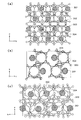
Sr3Al3Si13O2N21結晶は斜方晶系で、格子定数は、a=9.037(6)Å、b=14.734(9)Å、c=14.928(10)Åであり、図2に示すXRDプロファイルを呈する。この結晶は空間群P212121(非特許文献1に示された空間群のうちの19番目)に属する。なお、結晶の空間群は単結晶XRDにより決定することができる。Sr3Al3Si13O2N21結晶の結晶構造は図3に示す通りである。 The Sr 3 Al 3 Si 13 O 2 N 21 crystal is orthorhombic and the lattice constants are a = 9.037 (6) Å, b = 14.734 (9) Å, c = 14.928 (10). It is a spider and exhibits the XRD profile shown in FIG. This crystal belongs to the space group P2 1 2 1 2 1 (the 19th among the space groups shown in Non-Patent Document 1). Note that the crystal space group can be determined by single crystal XRD. The crystal structure of the Sr 3 Al 3 Si 13 O 2 N 21 crystal is as shown in FIG.
本発明による蛍光体は、X線回折や中性子回折により同定することができる。すなわち、ここで示されるSr3Al3Si13O2N21のXRDプロファイルと同一のプロファイルを示す物質の他に、構成元素が他の元素と入れ替わることにより格子定数が一定範囲で変化したものも、本発明による蛍光体に包含されるものである。ここで、構成元素が他の元素で置き換わるものとは、Sr3Al3Si13O2N21結晶中のSrが元素Mおよび/または発光中心元素Rで、元素Siの位置が4価の元素からなる群、例えばGe、Sn、Ti、Zr、Hfからなる群から選ばれる1種または2種以上の元素で、Alの位置が3価の元素からなる群、例えばB、Ga、In、Sc、Y、La、Gd、Luからなる群から選ばれる1種または2種以上の元素で、OまたはNの位置がO、N、Cからなる群から選ばれる1種または2種以上の元素で置換された結晶のことである。また、AlがSiに互いに置き換わると同時に、OとNが置き換わった、例えばSr3Al2Si14ON22、Sr3AlSi15N23、Sr3Al4Si12O3N20、Sr3Al5Si11O4N19、Sr3Al6Si10O5N18等もSr3Al3Si13O2N21属結晶である。
The phosphor according to the present invention can be identified by X-ray diffraction or neutron diffraction. That is, in addition to the material showing the same profile as the XRD profile of Sr 3 Al 3 Si 13 O 2 N 21 shown here, there is also a material whose lattice constant is changed within a certain range by replacing the constituent elements with other elements. These are included in the phosphor according to the present invention. Here, the constituent element is replaced with another element when Sr in the Sr 3 Al 3 Si 13 O 2 N 21 crystal is the element M and / or the luminescent center element R, and the position of the element Si is a tetravalent element. A group consisting of, for example, one or more elements selected from the group consisting of Ge, Sn, Ti, Zr, and Hf, and a group in which the position of Al is a trivalent element, such as B, Ga, In, Sc One or more elements selected from the group consisting of Y, La, Gd, and Lu, and one or more elements selected from the group consisting of O, N, and C at the position of O or N It is a substituted crystal. At the same time when the Al is replaced with one another on Si, O and N are replaced, for example, Sr 3 Al 2 Si 14 ON 22 , Sr 3 AlSi 15 N 23, Sr 3 Al 4 Si 12 O 3
さらに、固溶量が小さい場合には、Sr3Al3Si13O2N21属結晶の簡便な判定方法として次の方法がある。新たな物質について測定したXRDプロファイルの回折ピーク位置が主要ピークについて一致した時に、当該結晶構造が同じものと特定することができる。主要ピークとしては、回折強度の強い10本程度で判断すると良い。 Furthermore, when the amount of solid solution is small, there is the following method as a simple determination method for Sr 3 Al 3 Si 13 O 2 N 21 group crystals. When the diffraction peak position of the XRD profile measured for a new substance coincides with the main peak, the crystal structure can be identified as the same. As the main peak, it is good to judge by about 10 having strong diffraction intensity.
実施形態にかかる蛍光体は、例えば、元素Mの窒化物、またはその他シアナミド等の炭化物、Alなどの元素M1やSiなどの元素M2の、窒化物、酸化物、または炭化物、および発光中心元素Rの酸化物、窒化物、または炭酸塩を出発原料として用いて、合成することができる。より具体的には、元素MとしてSrを含有し、発光中心元素RとしてEuを含有する蛍光体を目的とする場合には、Sr3N2、AlN、Si3N4、Al2O3およびEuNを出発原料として用いることができる。Sr3N2の代わりにCa3N2、Ba3N2、Sr2NあるいはSrN等、もしくはこれらの混合物を用いてもよい。これらを所望の組成になるように秤量混合し、得られた混合粉末を焼成することによって、目的の蛍光体が得られる。混合に当たっては、例えば、グローブボックス中で乳鉢混合するといった手法が挙げられる。また、るつぼの材質は、窒化ホウ素、窒化ケイ素、炭化ケイ素、カーボン、窒化アルミニウム、サイアロン、酸化アルミ、モリブデンあるいはタングステン等としてもよい。 The phosphor according to the embodiment includes, for example, a nitride of an element M, a carbide such as cyanamide, a nitride such as an element M 1 such as Al, or an element M 2 such as Si, and an emission center. It can be synthesized using an oxide, nitride, or carbonate of element R as a starting material. More specifically, when a phosphor containing Sr as the element M and Eu as the emission center element R is intended, Sr 3 N 2 , AlN, Si 3 N 4 , Al 2 O 3 and EuN can be used as a starting material. Instead of Sr 3 N 2 , Ca 3 N 2 , Ba 3 N 2 , Sr 2 N, SrN, or the like, or a mixture thereof may be used. These are weighed and mixed so as to have a desired composition, and the obtained mixed powder is fired to obtain the target phosphor. In mixing, for example, a technique of mixing a mortar in a glove box can be mentioned. The material of the crucible may be boron nitride, silicon nitride, silicon carbide, carbon, aluminum nitride, sialon, aluminum oxide, molybdenum, tungsten, or the like.
これらの出発原料の混合物を所定時間焼成して、目的の組成を有する蛍光体を得ることができる。焼成は、大気圧以上の圧力で行なうことが望ましい。窒化ケイ素の高温での分解を抑制するためには、5気圧以上がより好ましい。焼成温度は1500〜2000℃の範囲が好ましく、より好ましくは1800〜2000℃である。焼成温度が1500℃未満の場合には、目的とする蛍光体の形成が困難となることがある。一方、2000℃を越えると、材料あるいは生成物の昇華のおそれがある。また、原料のAlNが酸化されやすいことから、N2雰囲気中で焼成することが望まれるが、窒素および水素の混合雰囲気でもよい。 A phosphor having a target composition can be obtained by firing a mixture of these starting materials for a predetermined time. The firing is desirably performed at a pressure of atmospheric pressure or higher. In order to suppress decomposition of silicon nitride at a high temperature, 5 atmospheres or more is more preferable. The firing temperature is preferably in the range of 1500 to 2000 ° C, more preferably 1800 to 2000 ° C. If the firing temperature is less than 1500 ° C., it may be difficult to form the target phosphor. On the other hand, if it exceeds 2000 ° C., there is a risk of sublimation of the material or product. In addition, since the raw material AlN is easily oxidized, it is desired to fire in an N 2 atmosphere, but a mixed atmosphere of nitrogen and hydrogen may be used.
焼成後の粉体に洗浄等の後処理を必要に応じて施して、実施形態にかかる蛍光体が得られる。洗浄を行う場合には、例えば純水洗浄、酸洗浄により行なうことができる。 The phosphor according to the embodiment can be obtained by subjecting the fired powder to post-treatment such as washing as necessary. When washing is performed, for example, pure water washing or acid washing can be performed.
実施形態にかかる蛍光体は、緑色の発光を示すLEDだけではなく、白色LEDにも適用することができる。具体的には、前記した蛍光体に、ほかの波長の光を発光する複数種の蛍光体を組み合わせて用いることにより、白色光を得ることができる。例えば、紫外光によりそれぞれ赤色、黄色(または緑色)、青色に発光する複数種の蛍光体を組み合わせて用いることができる。あるいは、青色光により黄色に発光する蛍光体と、必要に応じて赤色に発光する蛍光体を組み合わせ、励起光である青色光と組み合わせることで白色発光を得ることもできる。 The phosphor according to the embodiment can be applied not only to an LED that emits green light but also to a white LED. Specifically, white light can be obtained by using a combination of a plurality of types of phosphors that emit light of other wavelengths in the aforementioned phosphor. For example, a plurality of phosphors that emit red, yellow (or green), and blue light by ultraviolet light can be used in combination. Alternatively, it is also possible to obtain white light emission by combining a phosphor that emits yellow light with blue light and a phosphor that emits red light as necessary and combining it with blue light that is excitation light.
本発明による蛍光体は、従来知られている任意の発光装置に用いることができる。図1は、本発明の一実施形態にかかる発光装置の断面を示すものである。 The phosphor according to the present invention can be used in any conventionally known light-emitting device. FIG. 1 shows a cross section of a light emitting device according to an embodiment of the present invention.
図1に示された発光装置においては、樹脂ステム200はリードフレームを成形してなるリード201およびリード202と、これに一体成形されてなる樹脂部203とを有する。樹脂部203は、上部開口部が底面部より広い凹部205を有しており、この凹部の側面には反射面204が設けられる。
In the light emitting device shown in FIG. 1, the
凹部205の略円形底面中央部には、発光チップ206がAgペースト等によりマウントされている。発光チップ206としては、例えば発光ダイオード、レーザダイオード等を用いることができる。さらには、紫外光を放射するものを用いることができ、特に限定されるものではない。紫外光以外にも、青色や青紫、近紫外光などの波長の光を発光可能なチップも使用可能である。例えば、GaN系等の半導体発光素子等を用いることができる。発光チップ206の電極(図示せず)は、Auなどからなるボンディングワイヤー207および208によって、リード201およびリード202にそれぞれ接続されている。なお、リード201および202の配置は、適宜変更することができる。
A
樹脂部203の凹部205内には、蛍光層209が配置される。この蛍光層209は、本発明の実施形態にかかる蛍光体210を、例えばシリコーン樹脂からなる樹脂層211中に5重量%から50重量%の割合で分散、もしくは沈降させることによって形成することができる。実施形態にかかる蛍光体には、共有結合性の高い酸窒化物が母体として用いられている。このため、本発明による蛍光体は一般に疎水性であり、樹脂との相容性が極めて良好である。したがって、樹脂と蛍光体との界面での散乱が著しく抑制されて、光取出し効率が向上する。
A
発光チップ206としては、n型電極とp型電極とを同一面上に有するフリップチップ型のものを用いることも可能である。この場合には、ワイヤーの断線や剥離、ワイヤーによる光吸収等のワイヤーに起因した問題を解消して、信頼性の高い高輝度な半導体発光装置が得られる。また、発光チップ206にn型基板を用いて、次のような構成とすることもできる。具体的には、n型基板の裏面にn型電極を形成し、基板上の半導体層上面にはp型電極を形成して、n型電極またはp型電極をリードにマウントする。p型電極またはn型電極は、ワイヤーにより他方のリードに接続することができる。発光チップ206のサイズ、凹部205の寸法および形状は、適宜変更することができる。
As the
本発明の実施形態にかかる発光装置は、図1に示したようなパッケージカップ型に限定されず、適宜変更することができる。具体的には、砲弾型LEDや表面実装型LEDの場合も、実施形態の蛍光体を適用して同様の効果を得ることができる。 The light emitting device according to the embodiment of the present invention is not limited to the package cup type as shown in FIG. 1, and can be appropriately changed. Specifically, in the case of a bullet-type LED or a surface-mounted LED, the same effect can be obtained by applying the phosphor of the embodiment.
以下、諸例により本発明をさらに詳細に説明するが、本発明はこれらの例のみに限定されるものではない。 Hereinafter, the present invention will be described in more detail with reference to various examples, but the present invention is not limited to only these examples.
実施例1
出発原料としてSr3N2、EuN、Si3N4、Al2O3およびAlNを用意した。これら各々2.676g、0.398g、6.080g、0.680g、0.683gをバキュームグローブボックス中で秤量後、めのう乳鉢内で乾式混合したものを、BNるつぼに充填し、7.5気圧のN2雰囲気中、1850℃で4時間焼成して、設計組成が(Sr0.92Eu0.08)3Al3Si13O2N21である蛍光体を合成した。
Example 1
Sr 3 N 2 , EuN, Si 3 N 4 , Al 2 O 3 and AlN were prepared as starting materials. Each of these 2.676 g, 0.398 g, 6.080 g, 0.680 g, and 0.683 g were weighed in a vacuum glove box and then dry mixed in an agate mortar, and filled in a BN crucible, and 7.5 atm. in N 2 atmosphere, and then calcined 4 hours at 1850 ° C., was synthesized design composition (Sr 0.92 Eu 0.08) phosphor is 3 Al 3 Si 13 O 2 N 21.
焼成後の蛍光体は、体色が黄緑色の粉体であり、ブラックライトで励起した結果、緑色発光が観察された。 The fired phosphor was a yellowish green powder, and as a result of excitation with black light, green light emission was observed.
実施例2
出発原料としてSr3N2、Ca3N2、EuN、Si3N4、Al2O3およびAlNを用意した。これら各々2.408g、0.136g、0.398g、6.080g、0.680g、0.683gをバキュームグローブボックス中で秤量後、めのう乳鉢内で乾式混合したものを、BNるつぼに充填し、7.5気圧のN2雰囲気中、1850℃で4時間焼成して、設計組成が(Sr0.828Ca0.092Eu0.08)3Al3Si13O2N21である蛍光体を合成した。
Example 2
Sr 3 N 2 , Ca 3 N 2 , EuN, Si 3 N 4 , Al 2 O 3 and AlN were prepared as starting materials. Each of these 2.408 g, 0.136 g, 0.398 g, 6.080 g, 0.680 g, and 0.683 g were weighed in a vacuum glove box and then dry mixed in an agate mortar, and filled in a BN crucible. N 2 atmosphere for 7.5 atm, and then calcined 4 hours at 1850 ° C., designing composition of (Sr 0.828 Ca 0.092 Eu 0.08) phosphor is 3 Al 3 Si 13 O 2 N 21 Synthesized.
焼成後の蛍光体は、体色が黄緑色の粉体であり、ブラックライトで励起した結果、緑色発光が観察された。 The fired phosphor was a yellowish green powder, and as a result of excitation with black light, green light emission was observed.
実施例3
出発原料としてSr3N2、Ca3N2、EuN、Si3N4、Al2O3およびAlNを用意した。これら各々2.141g、0.273g、0.398g、6.080g、0.680g、0.683gをバキュームグローブボックス中で秤量後、めのう乳鉢内で乾式混合したものを、BNるつぼに充填し、7.5気圧のN2雰囲気中、1850℃で4時間焼成して、設計組成が(Sr0.736Ca0.184Eu0.08)3Al3Si13O2N21である蛍光体を合成した。
Example 3
Sr 3 N 2 , Ca 3 N 2 , EuN, Si 3 N 4 , Al 2 O 3 and AlN were prepared as starting materials. Each of these 2.141 g, 0.273 g, 0.398 g, 6.080 g, 0.680 g, and 0.683 g was weighed in a vacuum glove box and then dry mixed in an agate mortar, and filled into a BN crucible. A phosphor having a design composition of (Sr 0.736 Ca 0.184 Eu 0.08 ) 3 A 13 Si 13 O 2 N 21 baked at 1850 ° C. for 4 hours in a N 2 atmosphere at 7.5 atm. Synthesized.
焼成後の蛍光体は、体色が黄緑色の粉体であり、ブラックライトで励起した結果、緑色発光が観察された。 The fired phosphor was a yellowish green powder, and as a result of excitation with black light, green light emission was observed.
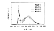
実施例1乃至3の黄緑色粉体について、解砕した後に458nmのピーク波長を有する発光ダイオードを光源に用いて励起した。得られた発光スペクトルは、図3に示す通りであった。図3において、458nmにピークを示すバンドは、励起光の反射によるものである。いずれの黄緑色粉体からも、515乃至530nmにピーク波長を有する単一バンドの発光が得られた。 The yellow-green powders of Examples 1 to 3 were excited using a light emitting diode having a peak wavelength of 458 nm as a light source after crushing. The obtained emission spectrum was as shown in FIG. In FIG. 3, a band having a peak at 458 nm is due to reflection of excitation light. From any of the yellowish green powders, single band emission having a peak wavelength at 515 to 530 nm was obtained.
実施例4
出発原料としてSr3N2、EuN、Si3N4、Al2O3およびAlNを用意した。これら各々2.408g、0.358g、5.893g、0.306g、0.492gをバキュームグローブボックス中で秤量後、めのう乳鉢内で乾式混合したものを、BNるつぼに充填し、7.5気圧のN2雰囲気中、1850℃で2時間焼成して、設計組成が(Sr0.92Eu0.08)3Al2Si14ON22である蛍光体を合成した。焼成後の蛍光体は、体色が黄緑色の粉体であり、ブラックライトで励起した結果、緑色発光が観察された。
Example 4
Sr 3 N 2 , EuN, Si 3 N 4 , Al 2 O 3 and AlN were prepared as starting materials. Each of these 2.408 g, 0.358 g, 5.893 g, 0.306 g, and 0.492 g was weighed in a vacuum glove box, and then dry mixed in an agate mortar, and filled in a BN crucible, and 7.5 atm. in N 2 atmosphere, and fired for two hours at 1850 ° C., it was synthesized design composition (Sr 0.92 Eu 0.08) phosphor is 3 Al 2 Si 14 ON 22. The fired phosphor was a yellowish green powder, and as a result of excitation with black light, green light emission was observed.
実施例5
出発原料としてSr3N2、EuN、Si3N4、Al2O3およびAlNを用意した。これら各々2.408g、0.358g、5.683g、0.459g、0.553gをバキュームグローブボックス中で秤量後、めのう乳鉢内で乾式混合したものを、BNるつぼに充填し、7.5気圧のN2雰囲気中、1850℃で4時間焼成して、設計組成が(Sr0.92Eu0.08)3Al2.5Si13.5O1.5N21.5である蛍光体を合成した。焼成後の蛍光体は、体色が黄緑色の粉体であり、ブラックライトで励起した結果、緑色発光が観察された。
Example 5
Sr 3 N 2 , EuN, Si 3 N 4 , Al 2 O 3 and AlN were prepared as starting materials. Each of these 2.408 g, 0.358 g, 5.683 g, 0.459 g, and 0.553 g was weighed in a vacuum glove box, and then dry mixed in an agate mortar, and filled in a BN crucible, and 7.5 atm. A phosphor having a design composition of (Sr 0.92 Eu 0.08 ) 3 Al 2.5 Si 13.5 O 1.5 N 21.5 is fired at 1850 ° C. for 4 hours in an N 2 atmosphere of Synthesized. The fired phosphor was a yellowish green powder, and as a result of excitation with black light, green light emission was observed.
実施例6
出発原料としてSr3N2、EuN、Si3N4、Al2O3およびAlNを用意した。これら各々2.408g、0.358g、5.262g、0.765g、0.676gをバキュームグローブボックス中で秤量後、めのう乳鉢内で乾式混合したものを、BNるつぼに充填し、7.5気圧のN2雰囲気中、1850℃で4時間焼成して、設計組成が(Sr0.92Eu0.08)3Al3.5Si12.5O2.5N20.5である蛍光体を合成した。焼成後の蛍光体は、体色が黄緑色の粉体であり、ブラックライトで励起した結果、緑色発光が観察された。
Example 6
Sr 3 N 2 , EuN, Si 3 N 4 , Al 2 O 3 and AlN were prepared as starting materials. Each of these 2.408 g, 0.358 g, 5.262 g, 0.765 g, and 0.676 g were weighed in a vacuum glove box and then dry mixed in an agate mortar, and filled in a BN crucible, and 7.5 atm. A phosphor having a designed composition of (Sr 0.92 Eu 0.08 ) 3 Al 3.5 Si 12.5 O 2.5 N 20.5 was fired at 1850 ° C. for 4 hours in an N 2 atmosphere of Synthesized. The fired phosphor was a yellowish green powder, and as a result of excitation with black light, green light emission was observed.
実施例7
出発原料としてSr3N2、EuN、Si3N4、Al2O3およびAlNを用意した。これら各々2.408g、0.358g、5.388g、0.673g、0.639gをバキュームグローブボックス中で秤量後、めのう乳鉢内で乾式混合したものを、BNるつぼに充填し、7.5気圧のN2雰囲気中、1850℃で4時間焼成して、設計組成が(Sr0.92Eu0.08)3Al3.2Si12.8O2.2N20.8である蛍光体を合成した。焼成後の蛍光体は、体色が黄緑色の粉体であり、ブラックライトで励起した結果、緑色発光が観察された。
Example 7
Sr 3 N 2 , EuN, Si 3 N 4 , Al 2 O 3 and AlN were prepared as starting materials. Each of these 2.408 g, 0.358 g, 5.388 g, 0.673 g, and 0.639 g was weighed in a vacuum glove box and then dry mixed in an agate mortar, and filled in a BN crucible, and 7.5 atm. A phosphor having a design composition of (Sr 0.92 Eu 0.08 ) 3 Al 3.2 Si 12.8 O 2.2 N 20.8 is fired at 1850 ° C. for 4 hours in an N 2 atmosphere of Synthesized. The fired phosphor was a yellowish green powder, and as a result of excitation with black light, green light emission was observed.
実施例8
出発原料としてSr3N2、EuN、Si3N4、Al2O3およびAlNを用意した。これら各々2.356g、0.448g、5.472g、0.612g、0.615gをバキュームグローブボックス中で秤量後、めのう乳鉢内で乾式混合したものを、BNるつぼに充填し、7.5気圧のN2雰囲気中、1850℃で4時間焼成して、設計組成が(Sr0.9Eu0.1)3Al3Si13O2N21である蛍光体を合成した。焼成後の蛍光体は、体色が黄緑色の粉体であり、ブラックライトで励起した結果、緑色発光が観察された。
Example 8
Sr 3 N 2 , EuN, Si 3 N 4 , Al 2 O 3 and AlN were prepared as starting materials. Each of these 2.356 g, 0.448 g, 5.472 g, 0.612 g, and 0.615 g was weighed in a vacuum glove box, and then dry mixed in an agate mortar, and filled in a BN crucible and 7.5 atm. Was fired at 1850 ° C. for 4 hours in a N 2 atmosphere, and a phosphor having a design composition of (Sr 0.9 Eu 0.1 ) 3 Al 3 Si 13 O 2 N 21 was synthesized. The fired phosphor was a yellowish green powder, and as a result of excitation with black light, green light emission was observed.
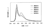
実施例4乃至8の黄緑色粉体について、解砕した後に460nmのピーク波長を有する発光ダイオードを光源に用いて励起した。得られた発光スペクトルは図4に示す通りであった。図4において、460nmにピークを示すバンドは、励起光の反射によるものである。いずれの黄緑色粉体からも、515乃至525nmにピーク波長を有する単一バンドの発光が得られた。 The yellow-green powders of Examples 4 to 8 were excited using a light-emitting diode having a peak wavelength of 460 nm as a light source after crushing. The obtained emission spectrum was as shown in FIG. In FIG. 4, the band having a peak at 460 nm is due to reflection of excitation light. From any of the yellowish green powders, single band emission having a peak wavelength at 515 to 525 nm was obtained.
実施例9
出発原料としてSr2N、EuN、Si3N4、Al2O3およびAlNを用意した。これら各々2.350g、0.358g、5.472g、0.612g、0.615gをバキュームグローブボックス中で秤量後、めのう乳鉢内で乾式混合したものを、BNるつぼに充填し、7.5気圧のN2雰囲気中、1850℃で4時間焼成して、設計組成が(Sr0.92Eu0.08)3Al3Si13O2N21である蛍光体を合成した。焼成後の蛍光体は、体色が黄緑色の粉体であり、ブラックライトで励起した結果、緑色発光が観察された。
Example 9
Sr 2 N, EuN, Si 3 N 4 , Al 2 O 3 and AlN were prepared as starting materials. Each of these 2.350 g, 0.358 g, 5.472 g, 0.612 g, and 0.615 g was weighed in a vacuum glove box and then dry mixed in an agate mortar, and filled in a BN crucible, and 7.5 atm. Was fired at 1850 ° C. for 4 hours in a N 2 atmosphere, to synthesize a phosphor having a design composition of (Sr 0.92 Eu 0.08 ) 3 Al 3 Si 13 O 2 N 21 . The fired phosphor was a yellowish green powder, and as a result of excitation with black light, green light emission was observed.
実施例10
出発原料としてSr2NとSr3N2が1:1の混合物、EuN、Si3N4、Al2O3およびAlNを用意した。これら各々2.379g、0.358g、5.472g、0.612g、0.615gをバキュームグローブボックス中で秤量後、めのう乳鉢内で乾式混合したものを、BNるつぼに充填し、7.5気圧のN2雰囲気中、1850℃で4時間焼成して、設計組成が(Sr0.92Eu0.08)3Al3Si13O2N21である蛍光体を合成した。焼成後の蛍光体は、体色が黄緑色の粉体であり、ブラックライトで励起した結果、緑色発光が観察された。
Example 10
As a starting material, a 1: 1 mixture of Sr 2 N and Sr 3 N 2 , EuN, Si 3 N 4 , Al 2 O 3 and AlN were prepared. Each of these 2.379 g, 0.358 g, 5.472 g, 0.612 g, and 0.615 g were weighed in a vacuum glove box and then dry mixed in an agate mortar, and filled in a BN crucible, and 7.5 atm. Was fired at 1850 ° C. for 4 hours in a N 2 atmosphere, to synthesize a phosphor having a design composition of (Sr 0.92 Eu 0.08 ) 3 Al 3 Si 13 O 2 N 21 . The fired phosphor was a yellowish green powder, and as a result of excitation with black light, green light emission was observed.
実施例11
出発原料としてSr2N、EuN、Si3N4、Al2O3およびAlNを用意した。これら各々2.325g、0.403g、5.472g、0.612g、0.615gをバキュームグローブボックス中で秤量後、めのう乳鉢内で乾式混合したものを、BNるつぼに充填し、7.5気圧のN2雰囲気中、1850℃で4時間焼成して、設計組成が(Sr0.91Eu0.09)3Al3Si13O2N21である蛍光体を合成した。焼成後の蛍光体は、体色が黄緑色の粉体であり、ブラックライトで励起した結果、緑色発光が観察された。
Example 11
Sr 2 N, EuN, Si 3 N 4 , Al 2 O 3 and AlN were prepared as starting materials. Each of these 2.325 g, 0.403 g, 5.472 g, 0.612 g, and 0.615 g were weighed in a vacuum glove box, and then dry mixed in an agate mortar, and filled in a BN crucible, and 7.5 atm. Was fired at 1850 ° C. for 4 hours in a N 2 atmosphere of No. 2 to synthesize a phosphor having a design composition of (Sr 0.91 Eu 0.09 ) 3 Al 3 Si 13 O 2 N 21 . The fired phosphor was a yellowish green powder, and as a result of excitation with black light, green light emission was observed.
実施例12
出発原料としてSr2N、EuN、Si3N4、Al2O3およびAlNを用意した。これら各々2.299g、0.448g、5.472g、0.612g、0.615gをバキュームグローブボックス中で秤量後、めのう乳鉢内で乾式混合したものを、BNるつぼに充填し、7.5気圧のN2雰囲気中、1850℃で4時間焼成して、設計組成が(Sr0.9Eu0.1)3Al3Si13O2N21である蛍光体を合成した。
Example 12
Sr 2 N as a starting material, EuN, was prepared Si 3 N 4, Al 2 O 3 , and AlN. Each of these 2.299 g, 0.448 g, 5.472 g, 0.612 g, and 0.615 g were weighed in a vacuum glove box and then dry mixed in an agate mortar, and filled in a BN crucible, and 7.5 atm. Was fired at 1850 ° C. for 4 hours in a N 2 atmosphere, and a phosphor having a design composition of (Sr 0.9 Eu 0.1 ) 3 Al 3 Si 13 O 2 N 21 was synthesized.
実施例9乃至12の黄緑色粉体について、解砕した後に460nmのピーク波長を有する発光ダイオードを光源に用いて励起した。得られた発光スペクトルは図5に示す通りであった。図5において、460nmにピークを示すバンドは、励起光の反射によるものである。いずれの黄緑色粉体からも、515乃至525nmにピーク波長を有する単一バンドの発光が得られた。 The yellow-green powders of Examples 9 to 12 were excited using a light emitting diode having a peak wavelength of 460 nm as a light source after crushing. The obtained emission spectrum was as shown in FIG. In FIG. 5, the band having a peak at 460 nm is due to reflection of excitation light. From any of the yellowish green powders, single band emission having a peak wavelength at 515 to 525 nm was obtained.
実施例1、5および7の黄緑色粉体の化学分析を行なった結果は下記表2に示す通りであった。下記表2には、前記一般式(B)におけるx、y、z、u、wおよびu−wの値を示した。 The results of chemical analysis of the yellow-green powders of Examples 1, 5 and 7 are as shown in Table 2 below. Table 2 below shows the values of x, y, z, u, w, and u−w in the general formula (B).
実施例1乃至12の黄緑色粉体の458nmもしくは460nm励起における吸収率、量子効率、および発光効率の値を、下記表3にまとめて示す。表2および3より本発明の蛍光体は高い量子効率を示すことが判る。特にzが0.2以上の場合には高い吸収率も同時に得られ、より好ましいことが判る。 The values of the absorptance, quantum efficiency, and light emission efficiency of the yellow-green powders of Examples 1 to 12 when excited at 458 nm or 460 nm are summarized in Table 3 below. Tables 2 and 3 show that the phosphor of the present invention exhibits high quantum efficiency. In particular, when z is 0.2 or more, a high absorption rate can be obtained at the same time, which is more preferable.
上記表3に示されるように、実施例1乃至12の黄緑色粉体は、いずれも波長250〜500nmの光で励起した際、490〜580nmの間に発光波長を有する蛍光体である。これらの蛍光体の吸収率、量子効率、および発光効率は、例えば(Ba、Sr)2SiO4:Eu等の従来の黄緑色蛍光体と同等以上である。 As shown in Table 3, the yellow-green powders of Examples 1 to 12 are phosphors having an emission wavelength of 490 to 580 nm when excited with light having a wavelength of 250 to 500 nm. The absorption rate, quantum efficiency, and light emission efficiency of these phosphors are equal to or higher than those of conventional yellow-green phosphors such as (Ba, Sr) 2 SiO 4 : Eu.
なお、特許文献1には、Eu付活βサイアロンの発光効率は、450nm励起で吸収率65%、内部量子効率53%、発光効率35%であることが記載されている。非特許文献2にも、同様の記載がある。こうした従来の蛍光体の発光効率と本実施形態の蛍光体の発光効率とを同一条件の励起波長で比較すると、本実施形態の緑色蛍光体の方が優れた特性を示すことがわかる。 Patent Document 1 describes that the luminous efficiency of Eu-activated β sialon has an absorption rate of 65%, an internal quantum efficiency of 53%, and a luminous efficiency of 35% when excited at 450 nm. Non-Patent Document 2 also has a similar description. When the luminous efficiency of such a conventional phosphor and the luminous efficiency of the phosphor of the present embodiment are compared at the excitation wavelength under the same conditions, it can be seen that the green phosphor of the present embodiment exhibits superior characteristics.
励起波長を254nm、365nm、および390nm、および460nmに変更した場合も、同様の波長範囲にピークを有する発光が確認された。励起波長が短すぎるとストークスシフトによる損失が大きくなり、励気波長が長過ぎると励起効率が低下することから、本発明による蛍光体を発光素子に用いる場合には励起波長は、380nm以上460nm以下であることが好ましい。また、発光のピーク波長は560nm以下であることが望まれる。 Even when the excitation wavelength was changed to 254 nm, 365 nm, 390 nm, and 460 nm, light emission having a peak in the same wavelength range was confirmed. If the excitation wavelength is too short, loss due to the Stokes shift increases, and if the excitation wavelength is too long, the excitation efficiency decreases. Therefore, when the phosphor according to the present invention is used in a light emitting device, the excitation wavelength is 380 nm or more and 460 nm or less. It is preferable that The peak wavelength of light emission is desirably 560 nm or less.
比較例1
出発原料としてSrCO3、AlN、Si3N4およびEu2O3を準備した。これらを各々16.298g、4.919g、26.659gおよび1.689g秤量し、脱水イソプロパノール(以下、IPAという)中で2hボールミル混合した。マントルヒーターで乾燥を行なうことにより、IPAを揮発・除去させた。その後、目開き300μmの篩を通して、原料粉を作製した。得られた原料粉を、目開き500〜1000μmの篩より自然落下させて、窒化ホウ素るつぼに充填した。るつぼに充填された原料粉は、7気圧のN2雰囲気中、1850℃で6時間焼成して蛍光体を合成した。
Comparative Example 1
SrCO 3, AlN as a starting material, was prepared Si 3 N 4 and Eu 2 O 3. These were weighed 16.298 g, 4.919 g, 26.659 g, and 1.689 g, respectively, and mixed in dehydrated isopropanol (hereinafter referred to as IPA) for 2 h by ball milling. IPA was volatilized and removed by drying with a mantle heater. Thereafter, raw material powder was produced through a sieve having an opening of 300 μm. The obtained raw material powder was naturally dropped from a sieve having an opening of 500 to 1000 μm and filled into a boron nitride crucible. The raw material powder filled in the crucible was baked at 1850 ° C. for 6 hours in a 7 atmosphere N 2 atmosphere to synthesize a phosphor.
焼成後の蛍光体は、体色の異なる2種類の焼結粉体の混合物であり、白色の焼結粉体と黄緑色の焼結粉体とが確認された。ブラックライトで励起した結果、白色粉体からは青色発光が観察され、黄緑色粉体からは緑色発光が観察された。 The phosphor after firing was a mixture of two types of sintered powders having different body colors, and a white sintered powder and a yellow-green sintered powder were confirmed. As a result of excitation with black light, blue light emission was observed from the white powder, and green light emission was observed from the yellow-green powder.
比較例2
出発原料としてSrCO3、AlN、Si3N4およびEu2O3を準備した。これらを各々14.940g、4.509g、28.296gおよび1.548g秤量し、脱水IPA中で2hボールミル混合した。マントルヒーターで乾燥を行なうことにより、IPAを揮発・除去させた。その後、目開き300μmの篩を通して、原料粉を作製した。得られた原料粉を、目開き500〜1000μmの篩より自然落下させて、窒化ホウ素るつぼに充填した。るつぼに充填された原料粉は、7気圧のN2雰囲気中、1800℃で16時間焼成して蛍光体を合成した。
Comparative Example 2
SrCO 3 , AlN, Si 3 N 4 and Eu 2 O 3 were prepared as starting materials. These were weighed 14.940 g, 4.509 g, 28.296 g and 1.548 g, respectively, and mixed for 2 h in a dehydrated IPA. IPA was volatilized and removed by drying with a mantle heater. Thereafter, raw material powder was produced through a sieve having an opening of 300 μm. The obtained raw material powder was naturally dropped from a sieve having an opening of 500 to 1000 μm and filled into a boron nitride crucible. The raw material powder filled in the crucible was baked at 1800 ° C. for 16 hours in a 7 atmosphere N 2 atmosphere to synthesize a phosphor.
焼成後の蛍光体は、体色の異なる2種類の焼結粉体の混合物であり、白色の焼結粉体と黄緑色の焼結粉体とが確認された。ブラックライトで励起した結果、白色粉体からは青色発光が観察され、黄緑色粉体からは緑色発光が観察された。 The phosphor after firing was a mixture of two types of sintered powders having different body colors, and a white sintered powder and a yellow-green sintered powder were confirmed. As a result of excitation with black light, blue light emission was observed from the white powder, and green light emission was observed from the yellow-green powder.
比較例3
出発原料としてSrCO3、AlN、Si3N4およびEu2O3を準備した。これらを各々25.097g、8.198g、46.77gおよび5.279g秤量し、脱水IPA中で2hボールミル混合した。マントルヒーターで乾燥を行なうことにより、IPAを揮発・除去させ、得られた原料粉を、カーボンるつぼに充填した。るつぼに充填された原料粉は、7気圧のN2雰囲気中、1750℃で36時間焼成して蛍光体を合成した。
Comparative Example 3
S r CO 3, AlN as a starting material, was prepared Si 3 N 4 and Eu 2 O3. These were weighed 25.097 g, 8.198 g, 46.77 g and 5.279 g, respectively, and mixed in a dehydrated IPA for 2 h in a ball mill. IPA was volatilized and removed by drying with a mantle heater, and the obtained raw material powder was filled in a carbon crucible. The raw material powder filled in the crucible was baked at 1750 ° C. for 36 hours in a 7 atmosphere N 2 atmosphere to synthesize a phosphor.
焼成後の蛍光体は、体色の異なる3種類の焼結粉体の混合物であり、白色の焼結粉体、赤色の焼結粉体、および黄緑色の焼結粉体が観察された。ブラックライトで励起した結果、白色粉体、赤色粉体、および黄緑色粉体からは、それぞれ青色発光、赤色発光、および緑色発光が観察された。 The phosphor after firing was a mixture of three types of sintered powders having different body colors, and a white sintered powder, a red sintered powder, and a yellow-green sintered powder were observed. As a result of excitation with black light, blue light emission, red light emission, and green light emission were observed from the white powder, red powder, and yellow-green powder, respectively.
比較例4
出発原料としてSrCO3、AlN、Si3N4およびEu2O3を準備した。これらを各々25.097g、8.198g、46.77gおよび5.279g秤量し、脱水IPA中で2hボールミル混合した。マントルヒーターで乾燥を行なうことにより、IPAを揮発・除去させ、得られた原料粉を、カーボンるつぼに充填した。るつぼに充填された原料粉は、7気圧のN2雰囲気中、1750℃で48時間焼成して蛍光体を合成した。
Comparative Example 4
SrCO 3 , AlN, Si 3 N 4 and Eu 2 O 3 were prepared as starting materials. These were weighed 25.097 g, 8.198 g, 46.77 g and 5.279 g, respectively, and mixed in a dehydrated IPA for 2 h in a ball mill. IPA was volatilized and removed by drying with a mantle heater, and the obtained raw material powder was filled in a carbon crucible. The raw material powder filled in the crucible was baked at 1750 ° C. for 48 hours in an N 2 atmosphere of 7 atm to synthesize a phosphor.
焼成後の蛍光体は、体色の異なる3種類の焼結粉体の混合物であり、白色の焼結粉体、赤色の焼結粉体、および黄緑色の焼結粉体が観察された。ブラックライトで励起した結果、白色粉体、赤色粉体、および黄緑色粉体からは、それぞれ青色発光、赤色発光、および緑色発光が観察された。 The phosphor after firing was a mixture of three types of sintered powders having different body colors, and a white sintered powder, a red sintered powder, and a yellow-green sintered powder were observed. As a result of excitation with black light, blue light emission, red light emission, and green light emission were observed from the white powder, red powder, and yellow-green powder, respectively.
比較例1乃至4の黄緑色粉体の化学分析を行なった結果は下記表4に示す通りであった。下記表4には、前記一般式(B)におけるx、y、zおよびuの値を示した。いずれも本発明において特定された組成範囲を逸脱していることが判る。 The results of chemical analysis of the yellow-green powders of Comparative Examples 1 to 4 are as shown in Table 4 below. Table 4 below shows the values of x, y, z, and u in the general formula (B). It turns out that all deviate from the composition range specified in the present invention.
比較例1乃至4の黄緑色粉体の457nm励起における吸収率、量子効率、および発光効率の値は下記表5に示す通りであった。いずれも本発明の量子効率を下回っており、本発明が量子効率の向上に顕著な効果があることが判る。 The values of absorptance, quantum efficiency, and luminous efficiency in 457 nm excitation of the yellow-green powders of Comparative Examples 1 to 4 are as shown in Table 5 below. Both are lower than the quantum efficiency of the present invention, and it can be seen that the present invention has a remarkable effect in improving the quantum efficiency.
実施例1および比較例1の蛍光体を、室温から200℃までヒーターにより試料温度を上昇させながら励起して、発光スペクトル変化を測定した。励起には、457nmのピーク波長を有する発光ダイオードを用いた。各温度における発光スペクトルのピーク強度の温度依存性は図7に示すとおりであった。 The phosphors of Example 1 and Comparative Example 1 were excited while increasing the sample temperature from room temperature to 200 ° C. with a heater, and the change in emission spectrum was measured. For excitation, a light emitting diode having a peak wavelength of 457 nm was used. The temperature dependence of the peak intensity of the emission spectrum at each temperature is as shown in FIG.
実施例1の蛍光体は比較例1の蛍光体に比べ、200℃の高温条件下でも、発光強度の低下が小さいことが図7のグラフに示されている。この結果から、本発明の実施形態にかかる蛍光体は、温度特性が顕著に改良されたものであることがわかる。図7のグラフには、実施例1の蛍光体についての結果を示したが、他の実施例にかかる蛍光体においても、同様に比較例を上回る良好な温度特性が得られた。 The graph of FIG. 7 shows that the phosphor of Example 1 has a smaller decrease in emission intensity than the phosphor of Comparative Example 1 even at a high temperature of 200 ° C. From this result, it can be seen that the phosphor according to the embodiment of the present invention has significantly improved temperature characteristics. The graph of FIG. 7 shows the results for the phosphor of Example 1. Also in the phosphors of other Examples, good temperature characteristics exceeding the comparative example were obtained.
また、実施例1の蛍光体を用いて、図1に示した発光装置を製造した。得られた発光装置を、室温から150℃の温度範囲で動作させ、効率の温度変化を測定したところ、この温度範囲で効率の低下が殆ど起こらなかった。このことから、実施形態にかかる蛍光体を用いた発光装置は、良好な温度特性を有することが確認された。 Further, using the phosphor of Example 1, the light emitting device shown in FIG. 1 was manufactured. The obtained light emitting device was operated in a temperature range from room temperature to 150 ° C., and the temperature change in efficiency was measured. As a result, there was almost no decrease in efficiency in this temperature range. From this, it was confirmed that the light-emitting device using the phosphor according to the embodiment has good temperature characteristics.
実施例13
発光ピーク波長449nmの発光ダイオードを、8mm角のAlNパッケージ上に半田を用いて接合し、金ワイヤーを介して電極に接続した。この発光ダイオード上にドーム状に透明樹脂を塗布し、その上にピーク波長585nmの赤色発光蛍光体(Ba0.1Sr0.8Ca0.1)2SiO4:Eu2+を40重量%混入させた透明樹脂を層状に塗布し、その上に実施例1の蛍光体を30重量%混入させた透明樹脂を層状に塗布して、図8に示された構造を有する発光装置を製造した。この発光装置を積分球内に設置し、20mA、3.1Vで駆動させたところ、色度(0.333,0.334)、色温度5450K、光束効率63.4lm/W、Ra=83であった。
Example 13
A light emitting diode having an emission peak wavelength of 449 nm was bonded onto an 8 mm square AlN package using solder and connected to an electrode via a gold wire. A transparent resin is applied on the light emitting diode in a dome shape, and 40% by weight of red light emitting phosphor (Ba 0.1 Sr 0.8 Ca 0.1 ) 2 SiO 4 : Eu 2+ having a peak wavelength of 585 nm is mixed thereon. The light-emitting device having the structure shown in FIG. 8 was manufactured by applying the transparent resin applied in a layered manner and applying the transparent resin mixed with 30% by weight of the phosphor of Example 1 in a layered manner. When this light emitting device was installed in an integrating sphere and driven at 20 mA, 3.1 V, chromaticity (0.333, 0.334), color temperature 5450K, luminous efficiency 63.4 lm / W, and Ra = 83. there were.
実施例14
発光ピーク波長449nmの発光ダイオードを、8mm角のAlNパッケージ上に半田を用いて接合し、金ワイヤーを介して電極に接続した。この発光ダイオード上にドーム状に透明樹脂を塗布し、その上にピーク波長585nmの赤色発光蛍光体(Ba0.1Sr0.8Ca0.1)2SiO4:Eu2+を60重量%混入させた透明樹脂を層状に塗布し、その上に実施例1の蛍光体を30重量%混入させた透明樹脂を層状に塗布して、発光装置を製造した。この発光装置を積分球内に設置し、20mA、3.1Vで駆動させたところ、色度(0.423,0.399)、色温度3200K、光束効率60.0lm/W、Ra=70であった。
Example 14
A light emitting diode having an emission peak wavelength of 449 nm was bonded onto an 8 mm square AlN package using solder and connected to an electrode via a gold wire. A transparent resin is applied on the light emitting diode in a dome shape, and 60% by weight of red light emitting phosphor (Ba 0.1 Sr 0.8 Ca 0.1 ) 2 SiO 4 : Eu 2+ having a peak wavelength of 585 nm is mixed thereon. The light-emitting device was manufactured by applying the transparent resin applied in layers and applying the transparent resin mixed with 30% by weight of the phosphor of Example 1 in layers. When this light emitting device was installed in an integrating sphere and driven at 20 mA, 3.1 V, chromaticity (0.423, 0.399), color temperature 3200 K, luminous efficiency 60.0 lm / W, and Ra = 70. there were.
実施例15
発光ピーク波長449nmの発光ダイオードを、8mm角のAlNパッケージ上に半田を用いて接合し、金ワイヤーを介して電極に接続した。この発光ダイオード上にドーム状に透明樹脂を塗布し、その上にピーク波長585nmの赤色発光蛍光体(Ba0.1Sr0.8Ca0.1)2SiO4:Eu2+を40重量%混入させた透明樹脂を層状に塗布し、その上に実施例1の蛍光体を20重量%混入させた透明樹脂を層状に塗布して、発光装置を製造した。この発光装置を積分球内に設置し、20mA、3.1Vで駆動させたところ、色度(0.354,0.329)、色温度4520K、光束効率61.6lm/W、Ra=81であった。
Example 15
A light emitting diode having an emission peak wavelength of 449 nm was bonded onto an 8 mm square AlN package using solder and connected to an electrode via a gold wire. A transparent resin is applied on the light emitting diode in a dome shape, and 40% by weight of red light emitting phosphor (Ba 0.1 Sr 0.8 Ca 0.1 ) 2 SiO 4 : Eu 2+ having a peak wavelength of 585 nm is mixed thereon. The light-emitting device was manufactured by applying the transparent resin thus applied in layers, and applying the transparent resin mixed with 20% by weight of the phosphor of Example 1 in layers. When this light-emitting device was installed in an integrating sphere and driven at 20 mA and 3.1 V, chromaticity (0.354, 0.329), color temperature 4520K, luminous efficiency 61.6 lm / W, and Ra = 81. there were.
実施例16
発光ピーク波長449nmの発光ダイオードを、8mm角のAlNパッケージ上に半田を用いて接合し、金ワイヤーを介して電極に接続した。この発光ダイオード上にドーム状に透明樹脂を塗布し、その上にピーク波長585nmの赤色発光蛍光体(Ba0.1Sr0.8Ca0.1)2SiO4:Eu2+を30重量%混入させた透明樹脂を層状に塗布し、その上に実施例1の蛍光体を30重量%混入させた透明樹脂を層状に塗布して、発光装置を製造した。この発光装置を積分球内に設置し、20mA、3.1Vで駆動させたところ、色度(0.298,0.305)、色温度7800K、光束効率62.2lm/W、Ra=86であった。
Example 16
A light emitting diode having an emission peak wavelength of 449 nm was bonded onto an 8 mm square AlN package using solder and connected to an electrode via a gold wire. A transparent resin is applied on the light emitting diode in the form of a dome, and a red light emitting phosphor (Ba 0.1 Sr 0.8 Ca 0.1 ) 2 SiO 4 : Eu 2+ having a peak wavelength of 585 nm is mixed on the light emitting diode. The light-emitting device was manufactured by applying the transparent resin applied in layers and applying the transparent resin mixed with 30% by weight of the phosphor of Example 1 in layers. When this light emitting device was installed in an integrating sphere and driven at 20 mA, 3.1 V, chromaticity (0.298, 0.305), color temperature 7800 K, luminous efficiency 62.2 lm / W, and Ra = 86. there were.
実施例17
発光ピーク波長449nmの発光ダイオードを、8mm角のAlNパッケージ上に半田を用いて接合し、金ワイヤーを介して電極に接続した。この発光ダイオード上にドーム状に透明樹脂を塗布し、その上にピーク波長600nmの赤色発光蛍光体(Sr0.7Ca0.3)2SiO4:Eu2+を40重量%混入させた透明樹脂を層状に塗布し、その上に透明樹脂を層状に塗布し、その上に、実施例1の蛍光体を40重量%混入させた透明樹脂を層状に塗布して、図9に示される構造を有する発光装置を製造した。この発光装置を積分球内に設置し、20mA、3.1Vで駆動させたところ、色度(0.337,0.372)、色温度5330K、光束効率62.2lm/W、Ra=87であった。
Example 17
A light emitting diode having an emission peak wavelength of 449 nm was bonded onto an 8 mm square AlN package using solder and connected to an electrode via a gold wire. A transparent resin in which a transparent resin is coated on the light emitting diode in a dome shape, and 40% by weight of red light emitting phosphor (Sr 0.7 Ca 0.3 ) 2 SiO 4 : Eu 2+ having a peak wavelength of 600 nm is mixed thereon. Is applied in layers, and a transparent resin is applied in layers thereon, and a transparent resin mixed with 40% by weight of the phosphor of Example 1 is applied in layers, and the structure shown in FIG. 9 is obtained. A light emitting device having the above was manufactured. When this light emitting device was installed in an integrating sphere and driven at 20 mA, 3.1 V, chromaticity (0.337, 0.372), color temperature 5330K, luminous efficiency 62.2 lm / W, Ra = 87. there were.
200 樹脂システム
201 リード
202 リード
203 樹脂部
204 反射面
205 凹部
206 発光チップ
207 ボンディングワイヤー
208 ボンディングワイヤー
209 蛍光層
210 蛍光体
211 樹脂層
301 Sr
302 SiまたはAl
303 OまたはN
304 SiまたはAlの占有率0.5のサイト
1701 AlNパッケージ
1702 発光ダイオード
1703 ボンディングワイヤー
1704 透明樹脂層
1705 赤色蛍光体層
1706 中間透明樹脂層
1707 緑色蛍光体層
200
302 Si or Al
303 O or N
304 Si or Al Occupation Site 0.5 1701
Claims (9)
前記元素M1が、IIIA族およびIIIB族から選ばれるものであり、
前記元素M2が、IVA族およびIVB族から選ばれるものである、請求項1に記載の蛍光体。 The metal element M is selected from a group IA element, a group IIA element, a group IIIA element, a group IIIB element, a rare earth element, and a group IVA element;
The element M 1 is selected from group IIIA and group IIIB;
The element M 2 is what is selected from Group IVA and IVB group, phosphor according to claim 1.
前記元素M1が、Al、B、Ga、In、Sc、Y、La、Gd、およびLuから選ばれるものであり、
前記元素M2が、Si、Ge、Sn、Ti、Zr、およびHfから選ばれるものである、請求項1または2に記載の蛍光体。 The metal element M is selected from Li, Na, K, Mg, Ca, Sr, Ba, B, Ga, In, Y, Sc, Gd, La, Lu, and Ge;
The element M 1 is, those selected Al, B, Ga, In, Sc, Y, La, Gd, and from Lu,
The element M 2 is, Si, Ge, Sn, Ti , Zr, and those selected from Hf, phosphor according to claim 1 or 2.
(M1−xRx)3−yAl3+zSi13−zO2+uN21−w (1)
(式中、MはIA族元素、IIA族元素、IIIA族元素、IIIB族元素、希土類元素、およびIVA族元素から選択される元素であり、
Rは、Eu、Ce、Mn、Tb、Yb、Dy、Sm、Tm、Pr、Nd、Pm、Ho、Er、Cr、Sn、Cu、Zn、As、Ag、Cd、Sb、Au、Hg、Tl、Pb、Bi、およびFeから選ばれる元素であり、
0<x≦1、
−0.1≦y≦0.15、
−1≦z≦1、
−1<u−w≦1)
で表わされる組成を有し、波長250〜500nmの光で励起した際に波長490〜580nmの間にピークを有する発光を示すことを特徴とする、請求項1に記載の蛍光体。 The following general formula (1):
(M 1-x R x ) 3-y Al 3 + z Si 13-z O 2 + u N 21-w (1)
(Wherein M is an element selected from Group IA elements, Group IIA elements, Group IIIA elements, Group IIIB elements, rare earth elements, and Group IVA elements;
R is Eu, Ce, Mn, Tb, Yb, Dy, Sm, Tm, Pr, Nd, Pm, Ho, Er, Cr, Sn, Cu, Zn, As, Ag, Cd, Sb, Au, Hg, Tl , Pb, Bi, and Fe,
0 <x ≦ 1,
−0.1 ≦ y ≦ 0.15,
−1 ≦ z ≦ 1,
−1 <u−w ≦ 1)
2. The phosphor according to claim 1, wherein the phosphor exhibits a light emission having a peak between wavelengths of 490 and 580 nm when excited by light having a wavelength of 250 to 500 nm.
前記発光素子上に配置された、請求項1〜6のいずれか1項に記載の蛍光体を含む蛍光体層と
を具備することを特徴とする発光装置。 A light emitting element that emits light having a wavelength of 250 nm to 500 nm;
A phosphor layer comprising the phosphor layer according to any one of claims 1 to 6 disposed on the light emitting element.
Priority Applications (4)
| Application Number | Priority Date | Filing Date | Title |
|---|---|---|---|
| JP2008197685A JP5592602B2 (en) | 2008-07-31 | 2008-07-31 | Phosphor and light emitting device using the same |
| US12/504,180 US8685277B2 (en) | 2008-07-31 | 2009-07-16 | Fluorescent substance and light-emitting device employing the same |
| US13/471,864 US8603361B2 (en) | 2008-07-31 | 2012-05-15 | Fluorescent substance and light-emitting device employing the same |
| US14/162,383 US20140138583A1 (en) | 2008-07-31 | 2014-01-23 | Fluorescent substance and light-emitting device employing the same |
Applications Claiming Priority (1)
| Application Number | Priority Date | Filing Date | Title |
|---|---|---|---|
| JP2008197685A JP5592602B2 (en) | 2008-07-31 | 2008-07-31 | Phosphor and light emitting device using the same |
Related Child Applications (2)
| Application Number | Title | Priority Date | Filing Date |
|---|---|---|---|
| JP2010183191A Division JP5592729B2 (en) | 2010-08-18 | 2010-08-18 | Phosphor and light emitting device using the same |
| JP2011103135A Division JP5398778B2 (en) | 2011-05-02 | 2011-05-02 | Method for manufacturing phosphor |
Publications (3)
| Publication Number | Publication Date |
|---|---|
| JP2010031201A true JP2010031201A (en) | 2010-02-12 |
| JP2010031201A5 JP2010031201A5 (en) | 2010-10-07 |
| JP5592602B2 JP5592602B2 (en) | 2014-09-17 |
Family
ID=41607385
Family Applications (1)
| Application Number | Title | Priority Date | Filing Date |
|---|---|---|---|
| JP2008197685A Active JP5592602B2 (en) | 2008-07-31 | 2008-07-31 | Phosphor and light emitting device using the same |
Country Status (2)
| Country | Link |
|---|---|
| US (3) | US8685277B2 (en) |
| JP (1) | JP5592602B2 (en) |
Cited By (28)
| Publication number | Priority date | Publication date | Assignee | Title |
|---|---|---|---|---|
| WO2010061597A1 (en) * | 2008-11-28 | 2010-06-03 | 昭和電工株式会社 | Illumination device for display devices and display device |
| WO2011016486A1 (en) * | 2009-08-06 | 2011-02-10 | 昭和電工株式会社 | Fluorescent substance, process for producing same, and luminescent device including same |
| WO2011102339A1 (en) * | 2010-02-16 | 2011-08-25 | 株式会社東芝 | White led for backlight of full-color liquid crystal display device, backlight for full-color liquid crystal display device, and full-color liquid crystal display device |
| JP2011168708A (en) * | 2010-02-19 | 2011-09-01 | Toshiba Corp | Fluorescent material and light-emitting device employing the same |
| WO2012023414A1 (en) * | 2010-08-19 | 2012-02-23 | 宇部興産株式会社 | Silicon nitride powder for siliconitride fluorescent material, sr3al3si13o2n21 fluorescent material and β-sialon fluorescent material both obtained using same, and processes for producing these |
| EP2423293A2 (en) | 2010-08-31 | 2012-02-29 | Kabushiki Kaisha Toshiba | Process for production of SiAlON oxynitride phosphors |
| WO2012036016A1 (en) * | 2010-09-17 | 2012-03-22 | 株式会社東芝 | Phosphor and light-emitting device |
| JP2012062440A (en) * | 2010-09-17 | 2012-03-29 | Toshiba Corp | Phosphor, method of manufacturing the same, and light-emitting device |
| CN102403438A (en) * | 2010-09-07 | 2012-04-04 | 株式会社东芝 | Light emitting device |
| JP2012077290A (en) * | 2010-09-07 | 2012-04-19 | Toshiba Corp | Light emitting device |
| JP2012099381A (en) * | 2010-11-04 | 2012-05-24 | Denki Kagaku Kogyo Kk | High intensity discharge lamp |
| JP2012162633A (en) * | 2011-02-06 | 2012-08-30 | National Institute For Materials Science | Phosphor, production method for same, and light-emitting device |
| JP2012197412A (en) * | 2011-03-09 | 2012-10-18 | Toshiba Corp | Phosphor, and light emitting device using the same |
| JP2012235145A (en) * | 2010-09-08 | 2012-11-29 | Toshiba Corp | Light-emitting device |
| WO2013054901A1 (en) * | 2011-10-12 | 2013-04-18 | 宇部興産株式会社 | Oxynitride fluorescent substance powder, silicon nitride powder for manufacturing same, and method for manufacturing same |
| US8471277B2 (en) | 2010-09-08 | 2013-06-25 | Kabushiki Kaisha Toshiba | Light emitting device |
| WO2013137434A1 (en) * | 2012-03-16 | 2013-09-19 | 株式会社東芝 | Phosphor, phosphor production method, and light-emitting device |
| JP2013538253A (en) * | 2010-07-22 | 2013-10-10 | ゼネラル・エレクトリック・カンパニイ | Oxynitride phosphor, manufacturing method, and light emitting device |
| US8558251B2 (en) | 2010-09-06 | 2013-10-15 | Kabushiki Kaisha Toshiba | Light emitting device |
| JP2013227587A (en) * | 2011-03-09 | 2013-11-07 | Toshiba Corp | Phosphor and light-emitting device using the same |
| US8608980B2 (en) | 2007-09-03 | 2013-12-17 | National Institute For Materials Science | Phosphor, method for producing the same and light-emitting device using the same |
| JP2014015597A (en) * | 2012-06-13 | 2014-01-30 | Toshiba Corp | Luminescent material and light-emitting device |
| KR101429345B1 (en) * | 2011-11-16 | 2014-08-11 | 가부시끼가이샤 도시바 | Luminescent material |
| US8937328B2 (en) | 2010-08-23 | 2015-01-20 | Kabushiki Kaisha Toshiba | Light emitting device and manufacturing method thereof |
| KR101487592B1 (en) | 2012-09-25 | 2015-01-29 | 가부시끼가이샤 도시바 | Fluorescent substance, light-emitting device and method for producing fluorescent substance |
| WO2017030030A1 (en) * | 2015-08-19 | 2017-02-23 | 宇部興産株式会社 | Fluorescent body, production method therefor and light-emitting device |
| JP2017125857A (en) * | 2012-06-13 | 2017-07-20 | 株式会社東芝 | Characteristic evaluation method for fluophor |
| JP2018095783A (en) * | 2016-12-15 | 2018-06-21 | 国立研究開発法人物質・材料研究機構 | Phosphor and light emitting device |
Families Citing this family (19)
| Publication number | Priority date | Publication date | Assignee | Title |
|---|---|---|---|---|
| JP5592602B2 (en) * | 2008-07-31 | 2014-09-17 | 株式会社東芝 | Phosphor and light emitting device using the same |
| KR101172143B1 (en) * | 2009-08-10 | 2012-08-07 | 엘지이노텍 주식회사 | OXYNITRIDE-BASED PHOSPHORS COMPOSING OF SiON ELEMENT FOR WHITE LEDs, MANUFACTURING METHOD THEREOF AND LEDs USING THE SAME |
| WO2011024296A1 (en) * | 2009-08-28 | 2011-03-03 | 株式会社 東芝 | Process for producing fluorescent substance and fluorescent substance produced thereby |
| US9909058B2 (en) * | 2009-09-02 | 2018-03-06 | Lg Innotek Co., Ltd. | Phosphor, phosphor manufacturing method, and white light emitting device |
| JP2011199193A (en) * | 2010-03-23 | 2011-10-06 | Toshiba Corp | Light emitting device and method of manufacturing the same |
| JP5101650B2 (en) * | 2010-03-25 | 2012-12-19 | 株式会社東芝 | Semiconductor light emitting device and manufacturing method thereof |
| JP5127965B2 (en) * | 2010-09-02 | 2013-01-23 | 株式会社東芝 | Phosphor and light emitting device using the same |
| JP5127964B2 (en) | 2010-09-06 | 2013-01-23 | 株式会社東芝 | Light emitting device |
| US8414145B2 (en) | 2010-09-06 | 2013-04-09 | Kabushiki Kaisha Toshiba | Light emitting device |
| JP5172915B2 (en) * | 2010-09-07 | 2013-03-27 | 株式会社東芝 | Light emitting device |
| JP5787343B2 (en) * | 2011-02-06 | 2015-09-30 | 国立研究開発法人物質・材料研究機構 | Phosphor and light emitting device |
| JP5690159B2 (en) * | 2011-02-06 | 2015-03-25 | 独立行政法人物質・材料研究機構 | Phosphor, method for manufacturing the same, and light emitting device |
| JP5634352B2 (en) * | 2011-08-24 | 2014-12-03 | 株式会社東芝 | Phosphor, light emitting device, and method of manufacturing phosphor |
| JP6010638B2 (en) * | 2013-01-23 | 2016-10-19 | シャープ株式会社 | Light emitting device |
| JP2014181260A (en) * | 2013-03-18 | 2014-09-29 | Toshiba Corp | Phosphor, light-emitting device and method for producing phosphor |
| JP2014224182A (en) * | 2013-05-15 | 2014-12-04 | 株式会社東芝 | Phosphor, light-emitting device, and production method of phosphor |
| JP2015157919A (en) * | 2014-02-25 | 2015-09-03 | 株式会社東芝 | Phosphor, light-emitting device and method for producing phosphor |
| JP6645429B2 (en) * | 2014-08-07 | 2020-02-14 | 三菱ケミカル株式会社 | Phosphor, light emitting device, image display device and lighting device |
| CN111925532B (en) * | 2020-08-21 | 2021-08-13 | 河南理工大学 | Adjustable dual-mode composite fluorescent material and preparation method and anti-counterfeiting application thereof |
Citations (1)
| Publication number | Priority date | Publication date | Assignee | Title |
|---|---|---|---|---|
| WO2006093298A1 (en) * | 2005-03-04 | 2006-09-08 | Dowa Electronics Materials Co., Ltd. | Fluorescent substance and process for producing the same, and light emitting device using said fluorescent substance |
Family Cites Families (17)
| Publication number | Priority date | Publication date | Assignee | Title |
|---|---|---|---|---|
| JP3020652B2 (en) * | 1991-06-11 | 2000-03-15 | 三菱レイヨン株式会社 | Fresnel lens for multi-projector and manufacturing method thereof |
| JP4362625B2 (en) * | 2004-02-18 | 2009-11-11 | 独立行政法人物質・材料研究機構 | Method for manufacturing phosphor |
| JP3921545B2 (en) | 2004-03-12 | 2007-05-30 | 独立行政法人物質・材料研究機構 | Phosphor and production method thereof |
| WO2007105631A1 (en) * | 2006-03-10 | 2007-09-20 | Kabushiki Kaisha Toshiba | Phosphor and light-emitting device |
| JP5578597B2 (en) | 2007-09-03 | 2014-08-27 | 独立行政法人物質・材料研究機構 | Phosphor, method for manufacturing the same, and light emitting device using the same |
| JP5592602B2 (en) * | 2008-07-31 | 2014-09-17 | 株式会社東芝 | Phosphor and light emitting device using the same |
| JP5190475B2 (en) * | 2010-02-19 | 2013-04-24 | 株式会社東芝 | Phosphor and light emitting device using the same |
| JP5398657B2 (en) * | 2010-07-06 | 2014-01-29 | 株式会社東芝 | Light emitting device |
| JP5076017B2 (en) * | 2010-08-23 | 2012-11-21 | 株式会社東芝 | Light emitting device |
| JP4991958B2 (en) * | 2010-09-06 | 2012-08-08 | 株式会社東芝 | Light emitting device |
| US8414145B2 (en) * | 2010-09-06 | 2013-04-09 | Kabushiki Kaisha Toshiba | Light emitting device |
| US8436527B2 (en) * | 2010-09-07 | 2013-05-07 | Kabushiki Kaisha Toshiba | Light emitting device |
| JP4929413B2 (en) * | 2010-09-07 | 2012-05-09 | 株式会社東芝 | Light emitting device |
| JP5172915B2 (en) * | 2010-09-07 | 2013-03-27 | 株式会社東芝 | Light emitting device |
| EP2428543B1 (en) * | 2010-09-08 | 2013-05-08 | Kabushiki Kaisha Toshiba | Light emitting device |
| JP5319743B2 (en) * | 2010-09-08 | 2013-10-16 | 株式会社東芝 | Light emitting device |
| JP6285100B2 (en) * | 2012-06-13 | 2018-02-28 | アルパッド株式会社 | Phosphor and light emitting device |
-
2008
- 2008-07-31 JP JP2008197685A patent/JP5592602B2/en active Active
-
2009
- 2009-07-16 US US12/504,180 patent/US8685277B2/en active Active
-
2012
- 2012-05-15 US US13/471,864 patent/US8603361B2/en active Active
-
2014
- 2014-01-23 US US14/162,383 patent/US20140138583A1/en not_active Abandoned
Patent Citations (1)
| Publication number | Priority date | Publication date | Assignee | Title |
|---|---|---|---|---|
| WO2006093298A1 (en) * | 2005-03-04 | 2006-09-08 | Dowa Electronics Materials Co., Ltd. | Fluorescent substance and process for producing the same, and light emitting device using said fluorescent substance |
Cited By (52)
| Publication number | Priority date | Publication date | Assignee | Title |
|---|---|---|---|---|
| US8608980B2 (en) | 2007-09-03 | 2013-12-17 | National Institute For Materials Science | Phosphor, method for producing the same and light-emitting device using the same |
| US8550645B2 (en) | 2008-11-28 | 2013-10-08 | Showa Denko K.K. | Illumination device for display device, and display device |
| JP2010129906A (en) * | 2008-11-28 | 2010-06-10 | Showa Denko Kk | Illumination device for display device and display device |
| WO2010061597A1 (en) * | 2008-11-28 | 2010-06-03 | 昭和電工株式会社 | Illumination device for display devices and display device |
| WO2011016486A1 (en) * | 2009-08-06 | 2011-02-10 | 昭和電工株式会社 | Fluorescent substance, process for producing same, and luminescent device including same |
| JP2011037913A (en) * | 2009-08-06 | 2011-02-24 | Showa Denko Kk | Phosphor, manufacturing method therefor, and light emitting device using the same |
| US8674388B2 (en) | 2009-08-06 | 2014-03-18 | National Institute For Materials Science | Phosphor, method of manufacturing the same, and light-emitting device |
| JP5732038B2 (en) * | 2010-02-16 | 2015-06-10 | 株式会社東芝 | White LED for backlight of full-color liquid crystal display device, backlight for full-color liquid crystal display device, and full-color liquid crystal display device |
| JPWO2011102339A1 (en) * | 2010-02-16 | 2013-06-17 | 株式会社東芝 | White LED for backlight of full-color liquid crystal display device, backlight for full-color liquid crystal display device, and full-color liquid crystal display device |
| WO2011102339A1 (en) * | 2010-02-16 | 2011-08-25 | 株式会社東芝 | White led for backlight of full-color liquid crystal display device, backlight for full-color liquid crystal display device, and full-color liquid crystal display device |
| KR101434713B1 (en) * | 2010-02-19 | 2014-08-26 | 가부시끼가이샤 도시바 | Fluorescent material and light-emitting device empolying the same |
| TWI502051B (en) * | 2010-02-19 | 2015-10-01 | Toshiba Kk | Fluorescent material and light-emitting device empolying the same |
| US8501039B2 (en) | 2010-02-19 | 2013-08-06 | Kabushiki Kaisha Toshiba | Fluorescent material and light-emitting device employing the same |
| JP2011168708A (en) * | 2010-02-19 | 2011-09-01 | Toshiba Corp | Fluorescent material and light-emitting device employing the same |
| JP2013538253A (en) * | 2010-07-22 | 2013-10-10 | ゼネラル・エレクトリック・カンパニイ | Oxynitride phosphor, manufacturing method, and light emitting device |
| WO2012023414A1 (en) * | 2010-08-19 | 2012-02-23 | 宇部興産株式会社 | Silicon nitride powder for siliconitride fluorescent material, sr3al3si13o2n21 fluorescent material and β-sialon fluorescent material both obtained using same, and processes for producing these |
| US9023241B2 (en) | 2010-08-19 | 2015-05-05 | Ube Industries, Ltd | Silicon nitride powder for siliconnitride phosphor, Sr3Al3Si13O2N21 phosphor and β-sialon phosphor both obtained using same, and processes for producing these |
| EP2615060A4 (en) * | 2010-08-19 | 2016-02-24 | Ube Industries | Silicon nitride powder for siliconitride fluorescent material, sr3al3si13o2n21 fluorescent material and beta-sialon fluorescent material both obtained using same, and processes for producing these |
| JP5874635B2 (en) * | 2010-08-19 | 2016-03-02 | 宇部興産株式会社 | Silicon nitride powder for silicon nitride phosphor, Sr3Al3Si13O2N21 phosphor using the same, β-sialon phosphor and method for producing the same |
| KR101762473B1 (en) * | 2010-08-19 | 2017-07-27 | 우베 고산 가부시키가이샤 | SILICON NITRIDE POWDER FOR SILICONITRIDE FLUORESCENT MATERIAL, SR3AL3SI13O2N21 FLUORESCENT MATERIAL AND β-SIALON FLUORESCENT MATERIAL BOTH OBTAINED USING SAME, AND PROCESSES FOR PRODUCING THESE |
| US8937328B2 (en) | 2010-08-23 | 2015-01-20 | Kabushiki Kaisha Toshiba | Light emitting device and manufacturing method thereof |
| US8628686B2 (en) | 2010-08-31 | 2014-01-14 | Kabushiki Kaisha Toshiba | Process for production of fluorescent substance |
| JP2012072346A (en) * | 2010-08-31 | 2012-04-12 | Toshiba Corp | Process for production of fluorescent substance |
| US8877095B2 (en) | 2010-08-31 | 2014-11-04 | Kabushiki Kaisha Toshiba | Process for production of fluorescent substance |
| EP2423293A2 (en) | 2010-08-31 | 2012-02-29 | Kabushiki Kaisha Toshiba | Process for production of SiAlON oxynitride phosphors |
| US8558251B2 (en) | 2010-09-06 | 2013-10-15 | Kabushiki Kaisha Toshiba | Light emitting device |
| US8436527B2 (en) | 2010-09-07 | 2013-05-07 | Kabushiki Kaisha Toshiba | Light emitting device |
| US8921878B2 (en) | 2010-09-07 | 2014-12-30 | Kabushiki Kaisha Toshiba | Light emitting device |
| JP2012077290A (en) * | 2010-09-07 | 2012-04-19 | Toshiba Corp | Light emitting device |
| CN102403438A (en) * | 2010-09-07 | 2012-04-04 | 株式会社东芝 | Light emitting device |
| US8471277B2 (en) | 2010-09-08 | 2013-06-25 | Kabushiki Kaisha Toshiba | Light emitting device |
| JP2012235145A (en) * | 2010-09-08 | 2012-11-29 | Toshiba Corp | Light-emitting device |
| JPWO2012036016A1 (en) * | 2010-09-17 | 2014-02-03 | 株式会社東芝 | Phosphor and light emitting device |
| JP2012062440A (en) * | 2010-09-17 | 2012-03-29 | Toshiba Corp | Phosphor, method of manufacturing the same, and light-emitting device |
| WO2012036016A1 (en) * | 2010-09-17 | 2012-03-22 | 株式会社東芝 | Phosphor and light-emitting device |
| KR101476561B1 (en) * | 2010-09-17 | 2014-12-24 | 가부시끼가이샤 도시바 | Phosphor and light-emitting device |
| JP2012099381A (en) * | 2010-11-04 | 2012-05-24 | Denki Kagaku Kogyo Kk | High intensity discharge lamp |
| JP2012162633A (en) * | 2011-02-06 | 2012-08-30 | National Institute For Materials Science | Phosphor, production method for same, and light-emitting device |
| JP2013227587A (en) * | 2011-03-09 | 2013-11-07 | Toshiba Corp | Phosphor and light-emitting device using the same |
| JP2012197412A (en) * | 2011-03-09 | 2012-10-18 | Toshiba Corp | Phosphor, and light emitting device using the same |
| WO2013054901A1 (en) * | 2011-10-12 | 2013-04-18 | 宇部興産株式会社 | Oxynitride fluorescent substance powder, silicon nitride powder for manufacturing same, and method for manufacturing same |
| US9758720B2 (en) | 2011-10-12 | 2017-09-12 | Ube Industries, Ltd. | Oxynitride phosphor powder, silicon nitride powder for production of oxynitride phosphor powder, and production method of oxynitride phosphor powder |
| JPWO2013054901A1 (en) * | 2011-10-12 | 2015-03-30 | 宇部興産株式会社 | Oxynitride phosphor powder, silicon nitride powder for producing oxynitride phosphor powder, and method for producing oxynitride phosphor powder |
| KR101429345B1 (en) * | 2011-11-16 | 2014-08-11 | 가부시끼가이샤 도시바 | Luminescent material |
| US9512359B2 (en) | 2012-03-16 | 2016-12-06 | Kabushiki Kaisha Toshiba | Phosphor, method for producing phosphor and light emitting device |
| WO2013137434A1 (en) * | 2012-03-16 | 2013-09-19 | 株式会社東芝 | Phosphor, phosphor production method, and light-emitting device |
| JPWO2013137434A1 (en) * | 2012-03-16 | 2015-08-03 | 株式会社東芝 | Phosphor, phosphor manufacturing method and light emitting device |
| JP2017125857A (en) * | 2012-06-13 | 2017-07-20 | 株式会社東芝 | Characteristic evaluation method for fluophor |
| JP2014015597A (en) * | 2012-06-13 | 2014-01-30 | Toshiba Corp | Luminescent material and light-emitting device |
| KR101487592B1 (en) | 2012-09-25 | 2015-01-29 | 가부시끼가이샤 도시바 | Fluorescent substance, light-emitting device and method for producing fluorescent substance |
| WO2017030030A1 (en) * | 2015-08-19 | 2017-02-23 | 宇部興産株式会社 | Fluorescent body, production method therefor and light-emitting device |
| JP2018095783A (en) * | 2016-12-15 | 2018-06-21 | 国立研究開発法人物質・材料研究機構 | Phosphor and light emitting device |
Also Published As
| Publication number | Publication date |
|---|---|
| US20100025632A1 (en) | 2010-02-04 |
| JP5592602B2 (en) | 2014-09-17 |
| US20140138583A1 (en) | 2014-05-22 |
| US8603361B2 (en) | 2013-12-10 |
| US20120229016A1 (en) | 2012-09-13 |
| US8685277B2 (en) | 2014-04-01 |
Similar Documents
| Publication | Publication Date | Title |
|---|---|---|
| JP5592602B2 (en) | Phosphor and light emitting device using the same | |
| JP5190475B2 (en) | Phosphor and light emitting device using the same | |
| JP4869317B2 (en) | Red phosphor and light emitting device using the same | |
| JP4762248B2 (en) | Phosphor | |
| TWI535825B (en) | Fluorescent substance and light-emitting device employing the same | |
| JP5129392B2 (en) | Method for producing phosphor and phosphor produced thereby | |
| JP4825923B2 (en) | Red phosphor and light emitting device using the same | |
| JP5592729B2 (en) | Phosphor and light emitting device using the same | |
| JP2013104041A (en) | Luminescent material, light-emitting device, and method for producing luminescent material | |
| JP5325959B2 (en) | Phosphor and light emitting device using the same | |
| JP5259770B2 (en) | Method for producing red phosphor | |
| JP5398778B2 (en) | Method for manufacturing phosphor | |
| JP2013216909A (en) | Phosphor | |
| JP2014224184A (en) | Phosphor and light-emitting device | |
| JP2013047347A (en) | Phosphor and light-emitting device using the same | |
| JP2013227587A (en) | Phosphor and light-emitting device using the same |
Legal Events
| Date | Code | Title | Description |
|---|---|---|---|
| A521 | Request for written amendment filed |
Free format text: JAPANESE INTERMEDIATE CODE: A523 Effective date: 20100818 |
|
| A621 | Written request for application examination |
Free format text: JAPANESE INTERMEDIATE CODE: A621 Effective date: 20100818 |
|
| A871 | Explanation of circumstances concerning accelerated examination |
Free format text: JAPANESE INTERMEDIATE CODE: A871 Effective date: 20100818 |
|
| A975 | Report on accelerated examination |
Free format text: JAPANESE INTERMEDIATE CODE: A971005 Effective date: 20100907 |
|
| A131 | Notification of reasons for refusal |
Free format text: JAPANESE INTERMEDIATE CODE: A131 Effective date: 20100928 |
|
| A521 | Request for written amendment filed |
Free format text: JAPANESE INTERMEDIATE CODE: A523 Effective date: 20101129 |
|
| A02 | Decision of refusal |
Free format text: JAPANESE INTERMEDIATE CODE: A02 Effective date: 20110204 |
|
| A521 | Request for written amendment filed |
Free format text: JAPANESE INTERMEDIATE CODE: A523 Effective date: 20110502 |
|
| A521 | Request for written amendment filed |
Free format text: JAPANESE INTERMEDIATE CODE: A821 Effective date: 20110531 |
|
| A911 | Transfer to examiner for re-examination before appeal (zenchi) |
Free format text: JAPANESE INTERMEDIATE CODE: A911 Effective date: 20110621 |
|
| A912 | Re-examination (zenchi) completed and case transferred to appeal board |
Free format text: JAPANESE INTERMEDIATE CODE: A912 Effective date: 20111021 |
|
| RD03 | Notification of appointment of power of attorney |
Free format text: JAPANESE INTERMEDIATE CODE: A7423 Effective date: 20140407 |
|
| A521 | Request for written amendment filed |
Free format text: JAPANESE INTERMEDIATE CODE: A821 Effective date: 20140407 |
|
| RD04 | Notification of resignation of power of attorney |
Free format text: JAPANESE INTERMEDIATE CODE: A7424 Effective date: 20140409 |
|
| A521 | Request for written amendment filed |
Free format text: JAPANESE INTERMEDIATE CODE: A523 Effective date: 20140613 |
|
| A61 | First payment of annual fees (during grant procedure) |
Free format text: JAPANESE INTERMEDIATE CODE: A61 Effective date: 20140801 |
|
| R151 | Written notification of patent or utility model registration |
Ref document number: 5592602 Country of ref document: JP Free format text: JAPANESE INTERMEDIATE CODE: R151 |