JP2010025989A - Optical scanner and image forming apparatus including the same - Google Patents
Optical scanner and image forming apparatus including the same Download PDFInfo
- Publication number
- JP2010025989A JP2010025989A JP2008183902A JP2008183902A JP2010025989A JP 2010025989 A JP2010025989 A JP 2010025989A JP 2008183902 A JP2008183902 A JP 2008183902A JP 2008183902 A JP2008183902 A JP 2008183902A JP 2010025989 A JP2010025989 A JP 2010025989A
- Authority
- JP
- Japan
- Prior art keywords
- plate member
- scanning device
- optical scanning
- beams
- deflecting
- Prior art date
- Legal status (The legal status is an assumption and is not a legal conclusion. Google has not performed a legal analysis and makes no representation as to the accuracy of the status listed.)
- Granted
Links
Images


Landscapes
- Facsimile Scanning Arrangements (AREA)
- Mechanical Optical Scanning Systems (AREA)
Abstract
Description
本発明は、LBP、デジタル複写機、またはデジタルFAX等の画像形成装置において、レーザービームを用いて光書き込みを行う光学走査装置、及びそれを備える画像形成装置に関する。 The present invention relates to an optical scanning apparatus that performs optical writing using a laser beam in an image forming apparatus such as an LBP, a digital copying machine, or a digital FAX, and an image forming apparatus including the optical scanning apparatus.
近年、画像形成装置のカラー化が進んでおり、特にモノクロと同じスピードで高速印刷が可能な、所謂タンデム方式の画像形成装置が広く知られている。タンデム方式とは、各トナー色ごとに光学走査系を設け、各々の光学走査系において形成されたトナー画像を重ね合わせて所望の画像を得る画像形成方式である。 In recent years, colorization of image forming apparatuses has progressed, and so-called tandem image forming apparatuses that can perform high-speed printing at the same speed as monochrome are widely known. The tandem method is an image forming method in which an optical scanning system is provided for each toner color and a desired image is obtained by superimposing toner images formed in the respective optical scanning systems.
このようなタンデム方式を有する画像形成装置として、複数の光学走査系に対して共通の回転多面鏡を備えるタイプのものが数多く提案されている。 Many types of image forming apparatuses having such a tandem method have been proposed which include a common rotary polygon mirror for a plurality of optical scanning systems.
その中でも回転多面鏡を、正弦波振動する1枚のミラーに置き換えたものが提案されている(特許文献1、特許文献2)。
Among them, the one in which the rotating polygon mirror is replaced with one mirror that vibrates sinusoidally has been proposed (
特許文献1には、4色分のビームを振動する1枚のミラーの片側面で偏向走査し、走査されたビームを色毎に分離して、各々の感光体の表面に導光する構成が開示されている。 Japanese Patent Application Laid-Open No. H10-260260 has a configuration in which a beam for four colors is deflected and scanned on one side of a single vibrating mirror, and the scanned beam is separated for each color and guided to the surface of each photoconductor. It is disclosed.
また、特許文献2には、振動する1枚の両面ミラーの両面を使ってビームを偏向走査し、偏向走査されたビームを色毎に分離して、各々のビームに対応して設けられた感光体の表面に導光する構成が開示されている。
In
さらに特許文献2には、両面ミラーを用いるタイプだけでなく、各々独立した片側鏡面のミラーを別々な揺動軸で軸支し、反鏡面側が向き合うように並べ、両面ミラーに近い形でビームの偏向走査を行う構成も開示されている。
しかしながら、上記従来の光学走査装置及びそれを備える画像形成装置では、以下に示す問題を生じる。 However, the conventional optical scanning device and the image forming apparatus including the same cause the following problems.
上記従来の光学走査装置では、揺動軸上に設けられたミラーは1枚(或いは2枚貼合せの一体もののミラー)である。 In the above-described conventional optical scanning device, the mirror provided on the swing shaft is a single sheet (or a two-piece laminated mirror).
よって、複数の光源から1枚のミラーにビームを精度よく入射させるためには、狭いスペースにミラー、レンズ等の入射系の部材を高精度に配置する必要があり、製造コストの増大を招く可能性がある。 Therefore, in order to make a beam accurately incident on a single mirror from a plurality of light sources, it is necessary to place incident members such as mirrors and lenses in a narrow space with high precision, which may increase manufacturing costs. There is sex.
一方で特許文献1、特許文献2には、複数の光源から射出されたビームをハーフミラー等を用いて合成し、合成して得られたビームを振動する1枚のミラーに入射させる構成が開示されている。
On the other hand,
しかし一般的にハーフミラーは高価であり、さらにハーフミラーの組付誤差によって生
じるミラー傾き角の2倍の角度でビームが傾いてしまうので、ハーフミラーは光路上に高精度に位置決めされる必要がある。その結果、ハーフミラーを用いる場合は製造コストが増大してしまう。
However, in general, the half mirror is expensive, and the beam is tilted at an angle twice the mirror tilt angle caused by the assembly error of the half mirror. Therefore, the half mirror needs to be positioned with high accuracy on the optical path. is there. As a result, when a half mirror is used, the manufacturing cost increases.
また、入射系の部材を傾けて配置することで、振動する1枚のミラー面上における偏向点を揃える構成も知られている。入射系の部材を傾ける方向としては、主走査方向に傾ける場合と、副走査方向に傾ける場合とが挙げられる。 A configuration is also known in which the deflection points on one mirror surface that vibrates are aligned by inclining and arranging the members of the incident system. As the direction in which the incident system member is tilted, there are a case of tilting in the main scanning direction and a case of tilting in the sub-scanning direction.
しかし、入射系の部材を主走査方向に傾けて並べて配置する場合は、揺動するミラーが静止状態になった際に、複数の光源から射出されるビームが全て異なる方向に偏向されてしまい、各々のビームの走査中心が異なってしまう。 However, when the incident members are arranged side by side in the main scanning direction, the beams emitted from the plurality of light sources are all deflected in different directions when the oscillating mirror is stationary. The scanning center of each beam is different.
また、正弦振動する1枚のミラーを用いて、偏向走査されるビームの速度が感光体上で等速度になるようにすると、走査レンズに、例えばf・arcsinθ特性を持たせる必要がある。 Further, if the speed of the beam to be deflected and scanned is made constant on the photosensitive member by using a single sine-vibrating mirror, the scanning lens needs to have, for example, f · arcsin θ characteristics.
しかし、4色全ての正弦波の位相が異なるので、4色全てのビームを感光体上で等速度にすることは困難である。 However, since the phases of the sine waves of all four colors are different, it is difficult to make the beams of all four colors have the same speed on the photosensitive member.
また、振動する1枚のミラーによってビームを偏向走査する際に、ミラーサイズを主走査方向に大きくしない場合は、ミラーの走査端で入射ビームの光束がミラー面上から外れてしまうといった、所謂ケラレが発生する。ケラレが発生すると、感光体上でスポットが肥大し、画像不良が生じる可能性がある。 Further, when the beam is deflected and scanned by a single vibrating mirror, if the mirror size is not increased in the main scanning direction, the so-called vignetting that the light beam of the incident beam deviates from the mirror surface at the scanning end of the mirror. Occurs. When vignetting occurs, the spots on the photoreceptor are enlarged, and image defects may occur.
一方で、入射系の部材を副走査方向に傾けて並べて配置する場合は、ミラーによって走査されたビームをそのまま感光体上まで導光すると、振動するミラーの揺動軸に直交した平面に対して傾いているビームほど、大きな走査線曲がりを有することになる。 On the other hand, when the incident members are arranged side by side in the sub-scanning direction, if the beam scanned by the mirror is directly guided onto the photoconductor, it is relative to a plane perpendicular to the oscillation axis of the vibrating mirror. A tilted beam will have a larger scan line bend.
つまり、それぞれの色に応じて大きな走査線曲がりを持つことになり、画像上では色毎に印字位置が異なってしまうので色ずれが生じてしまう。 That is, a large scanning line bend is caused according to each color, and the printing position is different for each color on the image, so that color misregistration occurs.
このような色ずれの発生を防ぐために、走査線曲がりを走査レンズで補正する方法があるが、あまりに補正量が多いと結像性能が劣化し、画像不良が生じる可能性がある。 In order to prevent the occurrence of such color misregistration, there is a method of correcting the scanning line curve with the scanning lens. However, if the correction amount is too large, the imaging performance may be deteriorated and an image defect may occur.
また、特許文献2のように走査ミラーの両面を用いてビームを偏向走査すると、走査ミラーの片面で偏向走査する入射系ビームは2色分で済むので、その分色ずれの発生は少なくなるが、それでも影響が無くなる訳ではない。
Further, when the beam is deflected and scanned using both sides of the scanning mirror as in
また、この影響を少なくするために副走査方向の傾け角を狭くすると、光源装置が並ぶピッチが狭くなり、互いのビームピッチが狭くなるので、ビーム同士が干渉する恐れがある。 Further, if the tilt angle in the sub-scanning direction is narrowed to reduce this influence, the pitch of the light source devices is narrowed and the beam pitch is narrowed, so that the beams may interfere with each other.
また、傾け角を狭くしすぎると、ビームピッチが狭すぎてビームの分離が困難になる。なお、入射系のビームピッチを狭めるためには、複数発光点を有する半導体レーザを用いる方法もあるが、ビームの分離はさらに困難なものとなる。 On the other hand, if the tilt angle is too narrow, the beam pitch is too narrow and beam separation becomes difficult. In order to narrow the beam pitch of the incident system, there is a method using a semiconductor laser having a plurality of light emitting points, but the beam separation becomes more difficult.
また、各ビームごとのミラー偏向点を副走査方向(振動するミラーの揺動軸方向)にずらすことで入射系の副走査ピッチを広げる方法もあるが、その方法によると、走査に用いるミラーサイズが大きくなってしまう。 In addition, there is a method of widening the sub-scanning pitch of the incident system by shifting the mirror deflection point for each beam in the sub-scanning direction (the oscillating axis direction of the oscillating mirror). Will become bigger.
ここで、ミラーサイズが大きくなった場合に生じる問題について説明する。 Here, a problem that occurs when the mirror size increases will be described.
ミラーの共振周波数は以下の式で表される。

上式において、fは共振周波数、Kはミラーを支持する梁(ねじりバネ)のバネ定数、Iはミラーの慣性モーメントである。ミラーサイズが大きくなると、慣性モーメントIが大きくなるので、上式より共振周波数fが小さくなる。 In the above equation, f is the resonance frequency, K is the spring constant of the beam (torsion spring) that supports the mirror, and I is the moment of inertia of the mirror. As the mirror size increases, the moment of inertia I increases, so the resonance frequency f decreases from the above equation.
共振周波数fが小さくなると、画像形成装置の書き込みスピードが低下し、スループットが落ちる、或いは解像度が低下し所望のスペックを満たさなくなるので、共振周波数fを元の値に維持するためには、バネ定数Kを上げる必要がある。 When the resonance frequency f is decreased, the writing speed of the image forming apparatus is decreased, the throughput is decreased, or the resolution is decreased and the desired specification is not satisfied. Therefore, in order to maintain the resonance frequency f at the original value, the spring constant It is necessary to raise K.
バネ定数Kを上げるためには、走査ミラーを支持するねじりバネの断面積を大きくすればよいが、ねじりバネの断面積を大きくすると、最大ねじれ角の時にバネにかかる応力が大きくなり、ねじりバネが破断する可能性がある。 In order to increase the spring constant K, it is only necessary to increase the cross-sectional area of the torsion spring that supports the scanning mirror. However, if the cross-sectional area of the torsion spring is increased, the stress applied to the spring at the maximum helix angle increases. May break.
従って、最大ねじれ時にバネにかかる応力を上げずにバネ定数を上げるには、ねじりバネを長くすることが考えられるが、ねじりバネを長くすると、光学走査装置が揺動軸方向に大型化してしまうという問題を生じる。 Therefore, in order to increase the spring constant without increasing the stress applied to the spring at the maximum torsion, it is conceivable to lengthen the torsion spring. However, if the torsion spring is lengthened, the optical scanning device becomes larger in the swing axis direction. This causes a problem.
この現状に鑑みて本発明は、ミラーサイズを大きくせずに入射系ピッチを広げることが可能な構成で、製造コストを低減しつつ、複数のビームを精度よく偏向走査することが可能な光学走査装置及びそれを備える画像形成装置を提供することを目的とする。 In view of this situation, the present invention is an optical scanning capable of widening the incident system pitch without increasing the mirror size, and capable of accurately deflecting and scanning a plurality of beams while reducing the manufacturing cost. It is an object to provide an apparatus and an image forming apparatus including the apparatus.
上記目的を達成するために本発明にあっては、
ビームを射出する複数の光源と、
前記複数の光源から射出されたビームをそれぞれのビームに対応して設けられた感光体の表面に偏向する光偏向ユニットと、
前記光偏向ユニットにおいて偏向されたビームを前記感光体の表面に結像する結像部材と、
を備える光学走査装置において、
前記光偏向ユニットは、
ビームの偏向を行うプレート部材と、
前記プレート部材を保持する保持部材と、
を有し、
前記プレート部材は、
ビームの偏向面が形成された偏向子と、
駆動力を受けて揺動する駆動子と、
前記プレート部材を前記保持部材に対して固定する固定部と、
を有し、
前記偏向子、前記駆動子、及び前記固定部がねじりバネによって直列に連結され、前記駆動子が駆動力を受けて揺動することに伴って前記偏向子が揺動する構成であって、
前記偏向子と前記駆動子は、
前記固定部を挟んで両側に前記固定部に対して対称となる配列でかつ、それぞれの揺動軸が一直線上にくるように設けられていることを特徴とする。
In order to achieve the above object, the present invention provides:
A plurality of light sources for emitting beams;
A light deflection unit that deflects the beams emitted from the plurality of light sources to the surface of the photoreceptor provided corresponding to each beam;
An imaging member for imaging the beam deflected in the light deflection unit on the surface of the photosensitive member;
In an optical scanning device comprising:
The light deflection unit is
A plate member for deflecting the beam;
A holding member for holding the plate member;
Have
The plate member is
A deflector formed with a deflection surface of the beam;
A driver that swings in response to a driving force;
A fixing portion for fixing the plate member to the holding member;
Have
The deflector, the driving element, and the fixed portion are connected in series by a torsion spring, and the deflecting element swings as the driving element swings by receiving a driving force,
The deflector and the driver are
It is characterized in that it is arranged on both sides of the fixed part so as to be symmetrical with respect to the fixed part, and the respective swing shafts are arranged in a straight line.
また、本発明に係る画像形成装置は、
上記の光学走査装置と、
前記光学走査装置から偏向されたビームが表面に結像される感光体と、
前記感光体に形成された画像をシート材上に転写する転写手段と、
を備えることを特徴とする。
An image forming apparatus according to the present invention is
The above optical scanning device;
A photoreceptor on which a beam deflected from the optical scanning device is imaged;
Transfer means for transferring an image formed on the photoreceptor onto a sheet material;
It is characterized by providing.
本発明によれば、ミラーサイズを大きくせずに入射系ピッチを広げることが可能な構成で、製造コストを低減しつつ、複数のビームを精度よく偏向走査することが可能な光学走査装置及びそれを備える画像形成装置を提供することができる。 According to the present invention, an optical scanning device capable of accurately deflecting and scanning a plurality of beams while reducing the manufacturing cost with a configuration capable of widening the incident system pitch without increasing the mirror size, and the same It is possible to provide an image forming apparatus including the above.
以下に図面を参照して、この発明を実施するための最良の形態を、実施の形態に基づいて例示的に詳しく説明する。ただし、この実施の形態に記載されている構成部品の寸法、材質、形状、その相対配置などは、特に特定的な記載がない限りは、この発明の範囲をそれらのみに限定する趣旨のものではない。 The best mode for carrying out the present invention will be exemplarily described in detail below based on the embodiments with reference to the drawings. However, the dimensions, materials, shapes, relative arrangements, and the like of the components described in this embodiment are not intended to limit the scope of the present invention only to those unless otherwise specified. Absent.
[第1の実施の形態]
図1〜図6を参照して、本発明の第1の実施の形態に係る光学走査装置及びそれを備える画像形成装置について説明する。
[First Embodiment]
With reference to FIGS. 1 to 6, an optical scanning device and an image forming apparatus including the same according to a first embodiment of the present invention will be described.
(画像形成装置の全体構成)
まず、本実施の形態に係る画像形成装置の全体構成について説明する。図6に本実施の形態に係る画像形成装置の概略構成を示す。
(Overall configuration of image forming apparatus)
First, the overall configuration of the image forming apparatus according to the present embodiment will be described. FIG. 6 shows a schematic configuration of the image forming apparatus according to the present embodiment.
画像形成を行う際は、画像情報に基づいて各々光変調されたビームLc、Lm、Ly、Lkが光学箱31から射出され、射出されたビームが、各々のビームに対応して設けられた感光ドラム(感光体)32c、32m、32y、32kの表面上に照射される。
When performing image formation, beams Lc, Lm, Ly, and Lk that are each light-modulated based on image information are emitted from the
各々の感光ドラムの表面は、一次帯電器33c、33m、33y、33kによって予め一様に帯電されており、帯電した表面にビームLc、Lm、Ly、Lkが照射されることで各々の感光ドラムの表面には静電潜像が形成される。
The surface of each photosensitive drum is uniformly charged in advance by
その後、感光ドラム32c、32m、32y、32kの表面に形成された静電潜像に対して現像器34c、34m、34y、34kからシアン、マゼンタ、イエロー、ブラックのトナーが供給され、静電潜像はトナー像として可視像化される。
Thereafter, cyan, magenta, yellow, and black toners are supplied from the developing
トナー像は感光ドラム32の回転とともに転写ベルト39(転写手段)上の位置まで搬送される。転写ベルト39は、各々の感光ドラム32の表面に形成されたトナー像が所定のタイミングでシート材36上に転写されるようにシート材36を搬送する。
The toner image is conveyed to a position on the transfer belt 39 (transfer means) as the
かかる画像形成プロセスによって、シート材36上にはシアン、マゼンタ、イエロー、ブラックのトナー像が順に重ね合わされて転写され、シート材上に所望のカラー画像が形成される。なお、転写ベルト39を駆動する駆動ローラ40は、転写ベルト39の送りを精度よく行うために、回転ムラの小さな駆動モータ(不図示)に接続されている。
By such an image forming process, cyan, magenta, yellow, and black toner images are sequentially superimposed and transferred onto the
所望のカラー画像が形成されたシート材36は定着器37に通紙され、定着器37においてカラー画像がシート材36上に熱定着される。その後、カラー画像が熱定着されたシート材36は排出ローラ38によって搬送され、画像形成装置の外部に出力される。
The
(光学走査装置の全体構成)
図5を参照して、本実施の形態に係る光学走査装置の全体構成について説明を行う。図5は、本実施の形態に係る光学走査装置の全体構成を示す斜視図である。
(Overall configuration of optical scanning device)
With reference to FIG. 5, the overall configuration of the optical scanning device according to the present embodiment will be described. FIG. 5 is a perspective view showing the overall configuration of the optical scanning device according to the present embodiment.
図5に示すように本実施の形態に係る光学走査装置は、ビームを射出する光源としての複数の半導体レーザ41c、41m、41y、41kと、射出された複数のビームを偏向走査する光偏向ユニット1とを備えている。
As shown in FIG. 5, the optical scanning device according to the present embodiment includes a plurality of
また上記構成に加え、光偏向ユニット1において偏向走査されたビームが透過するfθレンズ44cm、44ykと、ビームを反射する第1〜第3反射ミラーとを備えている。
Further, in addition to the above configuration,
なお、fθレンズ、第1〜第3反射ミラーは、感光ドラム32の表面にビームを結像する結像部材として設けられたものである。また、これらの結像部材と光偏向ユニット1は、不図示の光学箱に一体に収容されている。
The fθ lens and the first to third reflection mirrors are provided as image forming members for forming an image of the beam on the surface of the
上記構成によって、各々のビームに対応して設けられた感光ドラム32c、32m、32y、32kの表面にビームを結像する際は、まず、画像情報に基づいて半導体レーザ41c、41m、41y、41kからビームが射出される。
With the above configuration, when a beam is imaged on the surface of the
射出された計4本のビームは、光偏向ユニット1によって2本ずつ互いに異なる方向へ偏向走査される。偏向走査されたビームはそれぞれfθレンズ44cm、44ykを透過する。
A total of four emitted beams are deflected and scanned by the
例えば、fθレンズ44cmを透過した2本のビームのうち、半導体レーザ41cから射出されたビームは、第1反射ミラー45cで反射され、ビームLcとして感光ドラム32c上に結像する。
For example, of the two beams transmitted through the
一方、半導体レーザ41mから射出されたビームは、第2反射ミラー46m、第3反射ミラー47mで順次反射され、ビームLmとして感光ドラム32m上に結像する。
On the other hand, the beam emitted from the
同様に、fθレンズ44ykを透過した2本のビームのうち、半導体レーザ41kから射出されたビームは、第1反射ミラー45kで反射され、ビームLkとして感光ドラム32k上に結像する。
Similarly, of the two beams transmitted through the fθ lens 44yk, the beam emitted from the
また、半導体レーザ41yから射出されたビームは、第2反射ミラー46y、第3反射ミラー47yで順次反射され、ビームLyとして感光ドラム32y上に結像する。
The beam emitted from the
これら4本のビームが、半導体レーザ41から射出されてからそれぞれに対応して設けられた感光ドラム32上に結像するまで光路についてさらに詳細に説明する。
The optical path will be described in more detail after these four beams are emitted from the
半導体レーザ41c、41m、41y、41kから射出されたビームは、コリメータレンズ42c、42m、42y、42kによって平行光(コリメート光)化される。その後、これらのコリメート光はシリンドリカルレンズ43c、43m、43y、43kで副走査方向に圧縮され、光偏向ユニット1へ入射する。
Beams emitted from the
光偏向ユニット1の詳細な構成については後述するが、本実施の形態における光偏向ユニット1には、プレート部材2が備えられており、プレート部材2にはビームの偏向面が形成され揺動可能に構成された偏向子3u、3dが上下方向に1つずつ設けられている。
Although the detailed configuration of the
この偏向子にビームが入射すると、偏向子3u、3dに形成された偏向面には副走査方
向に圧縮されたビームが結像し、偏向面には線像が形成される。なお、本実施の形態における偏向子3u、3dには、表裏の両面に偏向面が形成されている。
When a beam is incident on the deflector, a beam compressed in the sub-scanning direction is formed on the deflecting surfaces formed on the
なお、これらの偏向子の表裏の偏向面と、各々の偏向面に対応して設けられた感光ドラム32c、32m、32y、32kの表面上は、副走査方向では互いに共役関係となるように構成されている。よって、偏向面の倒れ誤差に起因する感光ドラム32の表面上での副走査方向ビームの位置ズレ、いわゆる面倒れを低減させることが可能である。
The deflection surfaces on the front and back sides of these deflectors and the surfaces of the
また、半導体レーザ41から射出された4本のビームは、各々対応した感光ドラム32c、32m、32y、32k上に、最適に絞り込こまれたビームとして走査されるように、fθレンズ44cm、44ykにより調整されている。
Also, the four beams emitted from the
さらに、本実施の形態では、偏向子3uで偏向されたビームを2つのBDセンサ48mにより光検知し、偏向子3dで偏向されたビームを2つのBDセンサ48kにより光検知可能な構成とした。
Furthermore, in the present embodiment, the beam deflected by the
この構成によれば、BDセンサ48m、48kからの出力信号を基準に、4つのビームの走査回毎の書き込み信号を同期させ、ビームの書き込み位置を合わせることが可能になる。
According to this configuration, it is possible to synchronize the writing signals for the scanning times of the four beams and match the writing positions of the beams with reference to the output signals from the
また、BDセンサ48m、48kからの出力信号を用いて、偏向子3u、3dの走査振幅や走査周期を制御することも可能である。
It is also possible to control the scanning amplitude and scanning period of the
(光偏向ユニットの構成)
図1〜図4を参照して、本実施の形態に係る光学走査装置に備えられている光偏向ユニット1の構成、及びその作用について説明を行う。
(Configuration of light deflection unit)
With reference to FIGS. 1-4, the structure of the optical deflection |
図3、図4に示すように光偏向ユニット1は、ビームの偏向を行うプレート部材2と、単一のアクチュエータ9(駆動手段)と、これらを保持するホルダ8(保持部材)とを有している。
As shown in FIGS. 3 and 4, the
さらに、プレート部材2はビームの偏向面が形成された偏向子3u、3dと、駆動力を受ける駆動子4u、4dと、プレート部材2をホルダ8に対して固定する固定部12と、これらを直列に連結するねじりバネ5u、6u、6d、5dとを有している(図1)。なお、プレート部材2の構成については後述する。
Further, the
かかる構成を有する光偏向ユニット1は、ホルダ8に形成されたビス穴13を介して光学箱31にビス固定されている。
The
アクチュエータ9には、鉄心(コア)10に巻線(コイル)11を周回させたものが用いられている。このアクチュエータ9は、プレート部材2に設けられた駆動子4u、4dに駆動力を与え、駆動子4u、4dを揺動軸O周りに揺動させるためのものである。
As the actuator 9, an iron core (core) 10 around a winding (coil) 11 is used. The actuator 9 applies driving force to the
また、アクチュエータ9は、ホルダ8の略中央部に設けられた切欠き部14に挿入され、鉄心(コア)10の先端がこの切欠き部14に圧入されることで、ホルダ8に対して強固に固定されている。 In addition, the actuator 9 is inserted into a notch 14 provided at a substantially central portion of the holder 8, and the tip of the iron core (core) 10 is press-fitted into the notch 14, so that the holder 9 is firmly attached to the holder 8. It is fixed to.
すなわちアクチュエータ9は、プレート部材2の揺動軸O方向の略中央部に対向した位置に設けられている。なお、切欠き部14にアクチュエータ9を挿入する際は、アクチュエータ9がホルダ8の突当面15が当接するまで挿入される。
That is, the actuator 9 is provided at a position facing the substantially central portion of the
そして、このようにしてアクチュエータ9をホルダ8に組み付けた後、プレート部材2がホルダ8を挟んでアクチュエータ9に対して反対側(表側)からホルダ8に組み付けられる。プレート部材2を組み付ける際は、プレート部材2の固定部12を、ホルダ8に設けられた固定面14に対し接着固定することで組み付け作業が行われる。
After the actuator 9 is assembled to the holder 8 in this way, the
(プレート部材の構成)
図1を参照して、プレート部材2の構成について説明する。図1は、本実施の形態におけるプレート部材2の全体構成を示す斜視図である。
(Configuration of plate member)
The configuration of the
プレート部材2(素子)は、Si単結晶のウェハをエッチング加工して製作されるものである。上記でも説明したように、プレート部材2には偏向子3u、3dと駆動子4u、4dが備えられており、これらがねじりバネ6u、5u、5d、6dによって直列に連結されている。さらにプレート部材2の略中央部には固定部12が設けられている。
The plate member 2 (element) is manufactured by etching a Si single crystal wafer. As described above, the
なお、駆動子4u、4dには、棒状の永久磁石(マグネット)7が一体に固定されており、偏向子3u、3dには、表裏の両面にアルミ等が蒸着されている。このように偏向子の表面においてアルミ等が蒸着された表面は、ビームを反射するのに好適な偏向面となる。
In addition, rod-shaped permanent magnets (magnets) 7 are integrally fixed to the
また、本実施の形態では、固定部12を挟んで両側に固定部12に対して対称な配列となるように偏向子3u、3d、駆動子4u、4dを配列している点が特徴である。
In addition, the present embodiment is characterized in that the
すなわち、固定部12の上側には、固定部12に近いほうから順に駆動子4u、偏向子3uを配列させ、固定部12の下側には、固定部12に近いほうから順に駆動子4d、偏向子3dを配列させている。
That is, on the upper side of the fixed
また、偏向子3u、駆動子4u、固定部12、駆動子4d、偏向子3dが、ねじりバネ5u、6u、6d、5dによってこの順に直列に連結されており、さらに各々のねじりバネの揺動軸が一直線上にくるように設けられている。
Further, the
これにより固定部12を挟んで上下に設けられた偏向子、駆動子は、揺動軸O周りに同じ挙動を示すことになる。つまり、アクチュエータ9によって駆動子4u、4dが揺動されると、それに伴って上下の偏向子3u、3dも同様に揺動することが可能である。
Thereby, the deflector and the driver provided above and below the fixed
かかる構成を有するプレート部材2によってビームを偏向走査する場合について説明する。
A case where the beam is deflected and scanned by the
図1に示すように光源からのビームL1u、L2u、L1d、L2dは、それぞれプレート部材2の表裏側から偏向面に入射し、ビームL1u、L2uは偏向子3uで偏向され、ビームL1d、L2dは偏向子3dで偏向されている。
As shown in FIG. 1, the beams L1u, L2u, L1d, and L2d from the light source are incident on the deflecting surfaces from the front and back sides of the
また偏向子3u、3dは、駆動子4u、4dがアクチュエータ9から駆動力(ローレンツ力)を受けることで揺動軸O周りに、ねじりバネ6u、5u、5d、6dによってねじり振動(揺動)することが可能である。このように偏向子3u、3dが揺動軸O周りに揺動することで、ビームL1u、L2u、L1d、L2dを偏向走査することが可能である。
Further, the
なお、駆動子4u、4dは不図示の電源がアクチュエータ9の巻線(コイル)11を通電することで生じる駆動力(ローレンツ力)を受けて、揺動軸O周りに揺動する構成であ
るが、巻線11に通電される電流を振動モードに合わせて変調させることも可能である。
The
これにより、駆動子4u、4d及び偏向子3u、3dを、ねじりバネ5u、6u、5d、6dの揺動軸O周りに共振振動させることが可能になり、より精度良くビームを偏向走査することが可能になる。
As a result, the
図2を参照して、本実施の形態における偏向子3u、3dの挙動について説明する。図2は、縦軸を偏向子の振幅角度θ、横軸を時間tとした場合の、偏向子3u、3dの挙動の経時変化を示すものである。
With reference to FIG. 2, the behavior of the
光偏向ユニット1は、プレート部材2が有する複数の固有振動数(基本周波数ωと、基本周波数の2倍の周波数2ω)を重ね合わせた振動数で駆動される。すなわち、ビームの偏向に用いられる2つの偏向子3u、3dの挙動は以下の式で表される。なお、図2ではφ=0、A3=0としている。
The
θ(t)=A1sin(ωt)+A2sin(2ωt+φ)+A3
A1:基本周波数(基本波)成分における振幅
A2:基本周波数の2倍の周波数(倍波)成分における振幅
ω:基本周波数
φ:基本波と倍波の位相差
A3:静的な角度誤差、例えば初期の組付誤差などによる設計値からの誤差分
θ (t) = A 1 sin (ωt) + A 2 sin (2ωt + φ) + A 3
A 1 : Amplitude in fundamental frequency (fundamental wave) component A 2 : Amplitude in frequency (double wave) component twice the fundamental frequency ω: Fundamental frequency φ: Phase difference between fundamental wave and harmonic wave A 3 : Static angle Error, for example, error from design value due to initial assembly error
上式及び図2によれば、偏向子3u、3d、駆動子4u、4dの挙動が、基本周波数で同位相で振れるモードと、基本周波数の2倍の周波数での逆位相で振れるモードとを重ね合わせることで得られることを示している。
According to the above equation and FIG. 2, the behavior of the
また、各パラメータを適切に設定することにより、各周期内のある特定の範囲において、θ(t)≒kt+α(K、α:定数)と近似することが可能である。 Further, by appropriately setting each parameter, it is possible to approximate θ (t) ≈kt + α (K, α: constant) in a specific range within each cycle.
この範囲では、略等角速度(dθ/dt=k)で偏向子3u、3dが揺動することになり、図1におけるビームL1u、L1d、L2u、L2dはそれぞれある時間範囲で略等角速度で偏向走査されることになる。
In this range, the
(本実施の形態の作用効果)
本実施の形態では、固定部12を挟んで固定部12の両側に、固定部12に対して対称な配列となるように偏向子と駆動子とを設けた。また、それぞれの揺動軸を揺動軸Oとして一直線上にくるように設けた。この構成によると以下のような効果を奏する。
(Operational effect of the present embodiment)
In the present embodiment, the deflector and the driver are provided on both sides of the fixed
まず偏向子3u、3dが固定部12を挟んで十分に離間した状態になる。よって、ミラー面サイズを大きくすることなく、揺動軸O方向に各ビームの偏向点をずらすことが可能になる。また、アクチュエータ9が偏向子3u、3dに偏向されたビームを遮光する虞もない。
First, the
これにより、半導体レーザ41、コリメータレンズ42、シリンドリカルレンズ43からなる入射系の副走査方向のピッチを広げて入射系の部材を配置することが可能になる。
As a result, it is possible to dispose the incident system member by increasing the pitch in the sub-scanning direction of the incident system including the
また、入射系を副走査方向に傾ければ、さらに各入射系間のピッチを離して配置することができるので、プレート部材2のサイズをより小さくすることができる。この時、本実施の形態によると、入射系の副走査方向の傾け角は必要最小限にとどめることが可能になり、結像性能への影響を最小にとどめることができる。
Further, if the incident system is tilted in the sub-scanning direction, the pitch between the incident systems can be further increased, so that the size of the
また、偏向子3u、3dは固定部12を挟んで両側に十分に離間しているので、ねじりバネ5u、6u、6d、5dの長さも必要最小限の長さで済み、光学走査装置全体の揺動軸O方向、所謂副走査方向への大型化を防ぐことが出来る。
Further, since the
また、プレート部材2は1枚のSi単結晶ウェハから多数個取りで製作されるので、固定部12を挟んだ上下の偏向子3u、3d、駆動子4u、4dを同一の製造プロセスで製作することができる。
In addition, since the
よって、製造プロセスのばらつきに起因するウェハロット差が生じないので、上下の偏向子、駆動子間で形状誤差による相対差は生じにくい。その結果、固定部12を挟んだ両側の固有振動数が揃い、鏡面精度も揃い、走査特性も揃う。これにより、偏向走査されるビーム間にビーム特性上の差が生じにくく、良好な画像品質を実現することができる。
Therefore, since there is no wafer lot difference due to manufacturing process variations, relative differences due to shape errors are unlikely to occur between the upper and lower deflectors and drivers. As a result, the natural frequencies on both sides of the fixed
一方、固定部12を挟んだ上下の偏向子3u、3dを別体としてしまうと組付誤差や半導体の製造ばらつきによってそれぞれの偏向子の走査特性に差が生じる可能性があるが、本実施の形態では偏向子3u、3dが一体物であるので差が生じにくい。また、一体物であるので製造コストも低減可能である。
On the other hand, if the upper and
また、固定部12を挟んだ上下の偏向子3u、3d、駆動子4u、4dのそれぞれの揺動軸が同一直線上(揺動軸O)にあることで、上下の光学特性を揃えることも可能になっている。
Further, since the swing axes of the upper and
すなわち、それぞれの揺動軸が同一直線上でない場合は、不要なモーメントが生じて不要な振動モードを誘発したり、固定部12に不要応力が発生する虞もあるが、本実施の形態における構成によればこれらの不具合が低減される。
That is, if the respective swing axes are not on the same straight line, an unnecessary moment may be generated to induce an unnecessary vibration mode, or unnecessary stress may be generated in the fixed
また、プレート部材2を固定部12を挟んで上下で対称な配列とすることで、プレート部材2を揺動軸O方向の略中央部の一点で固定することが可能である。なお、固定部12の形状は本実施の形態における形状に限られるものではない。
Further, by arranging the
また、プレート部材2に設けられている全ての駆動子4u、4dを単一のアクチュエータ9によって駆動し、アクチュエータ9を揺動軸O方向の略中央部に配置しているので、部品数が削減され、光偏向ユニット1のサイズを最小限にすることも可能である。
Further, since all the
また、固定部12が揺動軸O方向の略中央部に設けられているので、プレート部材2全体のサイズを最小限にすることが可能である。
Further, since the fixed
また、ホルダ8の略中央部でプレート部材2の保持部がアクチュエータ9の保持部を兼ねていることで、プレート部材2とアクチュエータ9間の位置決め精度を向上させることができる。
Further, since the holding portion of the
また、偏向子3u、3dは略等角速度駆動となっているので、従来の回転多面鏡を用いた光学走査装置とほぼ同じ光学系を使用することが可能である。
Further, since the
また、本実施の形態では固定部12を挟んで上下に偏向子と駆動子を対称的に配列し、基本波と倍波の重ね合わせによる等角速度駆動としたが、正弦波駆動としてもよい。正弦波駆動の場合は、プレート部材2は基本波のみでの駆動となる。
Further, in the present embodiment, the deflector and the driver are arranged symmetrically up and down with the fixed
また、正弦波駆動の場合には、走査レンズには従来のfθレンズではなく、F・arc
sinθレンズを用いることで感光ドラム32の表面上でビームを等速走査することができる。
In the case of sine wave drive, the scanning lens is not a conventional fθ lens but F · arc.
By using the sin θ lens, the beam can be scanned at a constant speed on the surface of the
但し、F・arcsinθレンズを用いて等速化すると、左右の走査端ではビームスポット径が肥大してしまうので、別な方法としてF・arcsinθレンズを用いずに走査速度の変化に応じて画像書き込みクロックを滑らかに変化させる方法も挙げられる。 However, if the F. arcsin θ lens is used to make the speed constant, the beam spot diameter will be enlarged at the left and right scanning ends. As an alternative method, image writing can be performed according to changes in the scanning speed without using the F • arcsin θ lens. A method of smoothly changing the clock is also mentioned.
または、F・arcsinθに近いレンズでおおよそ等速走査とし、走査速度が若干変化してしまう分を画像書き込みタイミングで補正する、などという組合せ手段を採用することも可能である。 Alternatively, it is also possible to adopt a combination means such that a lens close to F · arcsin θ is set to scan at approximately constant speed, and the amount by which the scanning speed slightly changes is corrected at the image writing timing.
以上より本実施の形態によれば、ミラーサイズを大きくしてねじりバネを長くし、光学走査装置が揺動軸方向に分厚くなってしまうことを防ぎつつ、効率的に入射ピッチを広げながら光学部品をレイアウトすることが可能になる。また、走査ミラー間の動作中の特性相互差も最小限に抑えることが可能になる。 As described above, according to this embodiment, the mirror size is increased and the torsion spring is lengthened to prevent the optical scanning device from becoming thicker in the direction of the swing axis, while effectively increasing the incident pitch, and the optical component. Can be laid out. Also, it is possible to minimize the characteristic difference during operation between the scanning mirrors.
従って、本実施の形態によれば、ミラーサイズを大きくせずに入射系ピッチを広げることが可能な構成で、製造コストを低減しつつ、複数のビームを精度よく偏向走査することが可能な光学走査装置及びそれを備える画像形成装置を提供することが可能になる。 Therefore, according to this embodiment, an optical system capable of accurately deflecting and scanning a plurality of beams while reducing the manufacturing cost with a configuration capable of widening the incident system pitch without increasing the mirror size. It becomes possible to provide a scanning device and an image forming apparatus including the same.
[第2の実施の形態]
図7、図8を参照して本発明の第2の実施の形態に係る光学走査装置及びそれを備える画像形成装置について説明する。図7は、本実施の形態におけるプレート部材の全体構成を示す斜視図である。また、図8は、本実施の形態に係る光学走査装置の全体構成を示す斜視図である。なお、上記第1の実施の形態と同一の構成である部分については説明を省略する。
[Second Embodiment]
An optical scanning apparatus according to a second embodiment of the present invention and an image forming apparatus including the same will be described with reference to FIGS. FIG. 7 is a perspective view showing the overall configuration of the plate member in the present embodiment. FIG. 8 is a perspective view showing the overall configuration of the optical scanning device according to the present embodiment. Note that description of portions having the same configuration as in the first embodiment is omitted.
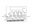
図7に示すように、本実施の形態は、偏向子の片面にのみ偏向面が形成されていることが特徴である。そして偏向子1つにつき、その片面にのみ偏向面が形成されているので、4本のビームを偏向走査するためにプレート部材2には4つの偏向子3c、3m、3y、3kが設けられている。また、第1の実施の形態と同様に、駆動子は固定部12の両側に1つずつ計2つ設けられている。
As shown in FIG. 7, the present embodiment is characterized in that a deflecting surface is formed only on one surface of the deflector. Since each deflector has a deflecting surface formed only on one surface thereof, the
そして偏向子3c、3m、3y、3kと駆動子4u、4dは、固定部12を挟んで両側に固定部12に対して対称となるように配列されており、偏向子3c、3m、3y、3kによって、ビームは二点鎖線Lc、Lm、Ly、Lkに偏向走査されている。また、各々の揺動軸が同一直線上にくるように配列されている点も第1の実施の形態と同様である。
The deflectors 3c, 3m, 3y, and 3k and the
図8に示すように、半導体レーザ41c、41m、41y、41kから射出されたビームは、コリメータレンズ42c、42m、42y、42kを透過し、その後、シリンドリカルレンズ43c、43m、43y、43kへと順次透過する。
As shown in FIG. 8, the beams emitted from the
その後、第1の実施の形態と異なり、各々のビームはプレート部材2の片側から各偏向面に対して入射し、偏向子3c、3m、3y、3kによって偏向走査される。その後、偏向面で偏向されたビームは走査レンズ44cm、44ykを透過し、第1折り返しミラー45c、45m、45y、45k、第2折り返しミラー46c、46m、46y、46kで順次折り返される。
Thereafter, unlike the first embodiment, each beam is incident on each deflection surface from one side of the
その後、ビームLc、Lm、Ly、Lkとなって、これらのビームが感光ドラム32c、32m、32y、32kの表面に照射される。なお、半導体レーザ41cから射出され
たビームは光書き込み領域外でBDセンサ48cに入射し、その出力信号は書き込み信号を同期させ、書き込み開始タイミングの検知に用いられている。また、偏向子3c、3m、3y、3kの振幅・周期の制御用検知に用いられてもよい。
Thereafter, beams Lc, Lm, Ly, and Lk are formed, and these beams are irradiated on the surfaces of the
本実施の形態によれば、偏向子の数が4つになるので、上記第1の実施の形態と比較すると光学走査装置の揺動軸O方向のサイズが大きくなるが、偏向子の片面のみを用いて偏向するので、偏向面の表裏の差が走査特性に影響を及ぼす虞がない。 According to this embodiment, since the number of deflectors is four, the size of the optical scanning device in the direction of the swing axis O is larger than that of the first embodiment, but only one side of the deflector. Therefore, there is no possibility that the difference between the front and back surfaces of the deflection surface will affect the scanning characteristics.
例えば、偏向子3c、3m、3y、3kの鏡面には、非常に高精度な平面性が求められる。しかし、素材のSi単結晶ウェハに反りがあったり、その後の半導体プロセスによって反りや歪みが発生すると、感光ドラム32c、32m、32y、32kの表面上でスポット形状が崩れる等の可能性がある。
For example, the mirror surfaces of the deflectors 3c, 3m, 3y, and 3k are required to have very high precision flatness. However, if the material Si single crystal wafer is warped or warped or distorted by the subsequent semiconductor process, the spot shape may collapse on the surfaces of the
また、偏向子の表裏両面を用いて偏向走査する場合は、表と裏で反りの方向が逆となるので、表面でのスポット形状と裏面でのスポット形状との間に相対差が生じ、それが画像品質に影響する場合がある。 Also, when deflecting scanning is performed using both the front and back sides of the deflector, the direction of warping is reversed between the front and back sides, so a relative difference occurs between the spot shape on the front surface and the spot shape on the back surface. May affect image quality.
これに対し本実施の形態では、偏向子の片面のみで偏向走査するので、各偏向面の反りの方向を揃えることができる。よって、走査レンズ44cm、44ykに設計上の補正を盛込む等の対応が可能になる。
In contrast, in the present embodiment, since deflection scanning is performed only on one side of the deflector, the direction of warping of each deflection surface can be made uniform. Therefore, it is possible to take measures such as incorporating design corrections into the
このように偏向面の反りの方向が揃うことによって、結像性能が各色で揃い、画像品質を向上させることが可能になる。また、偏向面に対する表面加工(偏向膜の形成など)が片面で済むので製造コストの低減にもつながる。 By aligning the warping directions of the deflection surfaces in this way, the imaging performance is uniform for each color, and the image quality can be improved. Further, since the surface processing (formation of a deflection film, etc.) on the deflection surface is completed on one side, the manufacturing cost can be reduced.
以上より、本実施の形態によれば、ミラーサイズを大きくしてねじりバネを長くし、光学走査装置が揺動軸方向に分厚くなってしまうことを防ぎつつ、効率的に入射ピッチを広げながら光学部品をレイアウトすることが可能になる。また、走査ミラー間の動作中の特性相互差も最小限に抑えることが可能になる。 As described above, according to the present embodiment, the mirror size is increased and the torsion spring is lengthened, and the optical scanning device is prevented from becoming thicker in the direction of the swing axis, and the optical pitch is efficiently increased while increasing the incident pitch. It becomes possible to lay out parts. Also, it is possible to minimize the characteristic difference during operation between the scanning mirrors.
従って、本実施の形態によれば、ミラーサイズを大きくせずに入射系ピッチを広げることが可能な構成で、製造コストを低減しつつ、複数のビームを精度よく偏向走査することが可能な光学走査装置及びそれを備える画像形成装置を提供することが可能になる。 Therefore, according to this embodiment, an optical system capable of accurately deflecting and scanning a plurality of beams while reducing the manufacturing cost with a configuration capable of widening the incident system pitch without increasing the mirror size. It becomes possible to provide a scanning device and an image forming apparatus including the same.
1 光偏向ユニット
2 プレート部材
3 偏向子
4 駆動子
5 ねじりバネ
6 ねじりバネ
7 永久磁石
8 ホルダ
9 アクチュエータ
12固定部
O 揺動軸
DESCRIPTION OF
Claims (4)
前記複数の光源から射出されたビームをそれぞれのビームに対応して設けられた感光体の表面に偏向する光偏向ユニットと、
前記光偏向ユニットにおいて偏向されたビームを前記感光体の表面に結像する結像部材と、
を備える光学走査装置において、
前記光偏向ユニットは、
ビームの偏向を行うプレート部材と、
前記プレート部材を保持する保持部材と、
を有し、
前記プレート部材は、
ビームの偏向面が形成された偏向子と、
駆動力を受けて揺動する駆動子と、
前記プレート部材を前記保持部材に対して固定する固定部と、
を有し、
前記偏向子、前記駆動子、及び前記固定部がねじりバネによって直列に連結され、前記駆動子が駆動力を受けて揺動することに伴って前記偏向子が揺動する構成であって、
前記偏向子と前記駆動子は、
前記固定部を挟んで両側に前記固定部に対して対称となる配列でかつ、それぞれの揺動軸が一直線上にくるように設けられていることを特徴とする光学走査装置。 A plurality of light sources for emitting beams;
A light deflection unit that deflects the beams emitted from the plurality of light sources to the surface of the photoreceptor provided corresponding to each of the beams;
An imaging member for imaging the beam deflected in the light deflection unit on the surface of the photosensitive member;
In an optical scanning device comprising:
The light deflection unit is
A plate member for deflecting the beam;
A holding member for holding the plate member;
Have
The plate member is
A deflector formed with a deflection surface of the beam;
A driver that swings in response to a driving force;
A fixing portion for fixing the plate member to the holding member;
Have
The deflector, the driving element, and the fixed portion are connected in series by a torsion spring, and the deflecting element swings as the driving element swings by receiving a driving force,
The deflector and the driver are
An optical scanning device, characterized in that it is arranged on both sides of the fixed portion so as to be symmetric with respect to the fixed portion, and the respective swing axes are aligned.
前記駆動手段は、
前記プレート部材の前記揺動軸方向の略中央部に対向した位置に設けられていることを特徴とする請求項1に記載の光学走査装置。 All the driving elements provided in the plate member are driven by a single driving means provided in the light deflection unit,
The driving means includes
The optical scanning device according to claim 1, wherein the optical scanning device is provided at a position facing a substantially central portion of the plate member in the swing axis direction.
前記保持部材を挟んで前記固定部の反対側に設けられていることを特徴とする請求項1または2に記載の光学走査装置。 The driving means includes
The optical scanning device according to claim 1, wherein the optical scanning device is provided on an opposite side of the fixing portion with the holding member interposed therebetween.
前記光学走査装置から偏向されたビームが表面に結像される感光体と、
前記感光体に形成された画像をシート材上に転写する転写手段と、
を備えることを特徴とする画像形成装置。 The optical scanning device according to any one of claims 1 to 3,
A photoreceptor on which a beam deflected from the optical scanning device is imaged;
Transfer means for transferring an image formed on the photoreceptor onto a sheet material;
An image forming apparatus comprising:
Priority Applications (1)
| Application Number | Priority Date | Filing Date | Title |
|---|---|---|---|
| JP2008183902A JP5264337B2 (en) | 2008-07-15 | 2008-07-15 | Optical scanning apparatus and image forming apparatus having the same |
Applications Claiming Priority (1)
| Application Number | Priority Date | Filing Date | Title |
|---|---|---|---|
| JP2008183902A JP5264337B2 (en) | 2008-07-15 | 2008-07-15 | Optical scanning apparatus and image forming apparatus having the same |
Publications (2)
| Publication Number | Publication Date |
|---|---|
| JP2010025989A true JP2010025989A (en) | 2010-02-04 |
| JP5264337B2 JP5264337B2 (en) | 2013-08-14 |
Family
ID=41731920
Family Applications (1)
| Application Number | Title | Priority Date | Filing Date |
|---|---|---|---|
| JP2008183902A Expired - Fee Related JP5264337B2 (en) | 2008-07-15 | 2008-07-15 | Optical scanning apparatus and image forming apparatus having the same |
Country Status (1)
| Country | Link |
|---|---|
| JP (1) | JP5264337B2 (en) |
Citations (3)
| Publication number | Priority date | Publication date | Assignee | Title |
|---|---|---|---|---|
| JP2006072292A (en) * | 2004-08-06 | 2006-03-16 | Ricoh Co Ltd | Optical scanning unit/image forming apparatus |
| JP2006292891A (en) * | 2005-04-07 | 2006-10-26 | Ricoh Co Ltd | Optical scanner and image forming apparatus using the same |
| JP2008040460A (en) * | 2006-02-13 | 2008-02-21 | Canon Inc | Oscillator device and optical deflecting device |
-
2008
- 2008-07-15 JP JP2008183902A patent/JP5264337B2/en not_active Expired - Fee Related
Patent Citations (3)
| Publication number | Priority date | Publication date | Assignee | Title |
|---|---|---|---|---|
| JP2006072292A (en) * | 2004-08-06 | 2006-03-16 | Ricoh Co Ltd | Optical scanning unit/image forming apparatus |
| JP2006292891A (en) * | 2005-04-07 | 2006-10-26 | Ricoh Co Ltd | Optical scanner and image forming apparatus using the same |
| JP2008040460A (en) * | 2006-02-13 | 2008-02-21 | Canon Inc | Oscillator device and optical deflecting device |
Also Published As
| Publication number | Publication date |
|---|---|
| JP5264337B2 (en) | 2013-08-14 |
Similar Documents
| Publication | Publication Date | Title |
|---|---|---|
| JP4963399B2 (en) | Image forming apparatus | |
| JP2010049259A (en) | Micro electro-mechanical system mirror, mirror scanner, optical scanning unit and image forming device using optical scanning unit | |
| JP4830470B2 (en) | Optical scanning device and image forming apparatus | |
| JP2006243034A (en) | Optical scanner and image forming apparatus | |
| JP4974846B2 (en) | Optical scanning apparatus and image forming apparatus having the same | |
| KR101474755B1 (en) | Image forming apparatus caparable of compensating for color registration error and method of compensating for color registration error | |
| JP2005017607A (en) | Light beam scanner and image forming device furnished with the same | |
| JP5264337B2 (en) | Optical scanning apparatus and image forming apparatus having the same | |
| KR101329745B1 (en) | Color registration corrected image forming apparatus and method | |
| JP6157128B2 (en) | Optical scanning apparatus and image forming apparatus | |
| JP4496747B2 (en) | Optical scanning apparatus and image forming apparatus | |
| JP4701593B2 (en) | Optical scanning apparatus and image forming apparatus | |
| JP2007178817A (en) | Method of adjusting optical scanner | |
| JP4572540B2 (en) | Optical scanning apparatus and image forming apparatus | |
| JP2011095458A (en) | Optical scanner and image forming apparatus equipped with the same | |
| JP2008282021A (en) | Optical scanner and image forming apparatus | |
| JP6614419B2 (en) | Optical scanning device and image forming apparatus including the optical scanning device | |
| JP4576816B2 (en) | Optical scanning apparatus and image forming apparatus | |
| JP4792960B2 (en) | Optical scanning device | |
| JP2005070708A (en) | Optical scanner and image forming apparatus | |
| JP2007196606A (en) | Image formation apparatus | |
| JP6669991B2 (en) | Optical scanning device and image forming apparatus provided with the optical scanning device | |
| JP2005115211A (en) | Optical scanner and image forming apparatus | |
| JP4774986B2 (en) | Method for adjusting optical scanning device | |
| JP2004287214A (en) | Exposure device and image forming apparatus |
Legal Events
| Date | Code | Title | Description |
|---|---|---|---|
| A621 | Written request for application examination |
Free format text: JAPANESE INTERMEDIATE CODE: A621 Effective date: 20110715 |
|
| A977 | Report on retrieval |
Free format text: JAPANESE INTERMEDIATE CODE: A971007 Effective date: 20120613 |
|
| A131 | Notification of reasons for refusal |
Free format text: JAPANESE INTERMEDIATE CODE: A131 Effective date: 20120619 |
|
| A521 | Written amendment |
Free format text: JAPANESE INTERMEDIATE CODE: A523 Effective date: 20120820 |
|
| A02 | Decision of refusal |
Free format text: JAPANESE INTERMEDIATE CODE: A02 Effective date: 20120904 |
|
| A521 | Written amendment |
Free format text: JAPANESE INTERMEDIATE CODE: A523 Effective date: 20121204 |
|
| A911 | Transfer of reconsideration by examiner before appeal (zenchi) |
Free format text: JAPANESE INTERMEDIATE CODE: A911 Effective date: 20130122 |
|
| TRDD | Decision of grant or rejection written | ||
| A01 | Written decision to grant a patent or to grant a registration (utility model) |
Free format text: JAPANESE INTERMEDIATE CODE: A01 Effective date: 20130402 |
|
| A61 | First payment of annual fees (during grant procedure) |
Free format text: JAPANESE INTERMEDIATE CODE: A61 Effective date: 20130430 |
|
| R151 | Written notification of patent or utility model registration |
Ref document number: 5264337 Country of ref document: JP Free format text: JAPANESE INTERMEDIATE CODE: R151 |
|
| LAPS | Cancellation because of no payment of annual fees |