JP2010023480A - Inkjet print head substrate, method for manufacturing inkjet print head substrate, inkjet print head, and inkjet recording apparatus - Google Patents
Inkjet print head substrate, method for manufacturing inkjet print head substrate, inkjet print head, and inkjet recording apparatus Download PDFInfo
- Publication number
- JP2010023480A JP2010023480A JP2009030896A JP2009030896A JP2010023480A JP 2010023480 A JP2010023480 A JP 2010023480A JP 2009030896 A JP2009030896 A JP 2009030896A JP 2009030896 A JP2009030896 A JP 2009030896A JP 2010023480 A JP2010023480 A JP 2010023480A
- Authority
- JP
- Japan
- Prior art keywords
- recording head
- ink
- ink jet
- electrode
- metal wiring
- Prior art date
- Legal status (The legal status is an assumption and is not a legal conclusion. Google has not performed a legal analysis and makes no representation as to the accuracy of the status listed.)
- Granted
Links
- 239000000758 substrate Substances 0.000 title claims abstract description 51
- 238000000034 method Methods 0.000 title claims description 15
- 238000004519 manufacturing process Methods 0.000 title claims description 4
- 238000001514 detection method Methods 0.000 claims abstract description 65
- 229910052751 metal Inorganic materials 0.000 claims abstract description 48
- 239000002184 metal Substances 0.000 claims abstract description 48
- 238000007789 sealing Methods 0.000 claims abstract description 19
- 239000011347 resin Substances 0.000 claims abstract description 18
- 229920005989 resin Polymers 0.000 claims abstract description 18
- 230000001681 protective effect Effects 0.000 claims description 33
- 238000009429 electrical wiring Methods 0.000 claims description 24
- 239000000463 material Substances 0.000 claims description 21
- 229910052782 aluminium Inorganic materials 0.000 claims description 11
- XAGFODPZIPBFFR-UHFFFAOYSA-N aluminium Chemical compound [Al] XAGFODPZIPBFFR-UHFFFAOYSA-N 0.000 claims description 11
- 238000010438 heat treatment Methods 0.000 claims description 10
- 238000005530 etching Methods 0.000 claims description 6
- 239000000203 mixture Substances 0.000 claims description 4
- 230000035945 sensitivity Effects 0.000 abstract description 6
- 230000009545 invasion Effects 0.000 abstract 1
- 239000010410 layer Substances 0.000 description 30
- 239000007788 liquid Substances 0.000 description 4
- 238000000206 photolithography Methods 0.000 description 4
- 229910004200 TaSiN Inorganic materials 0.000 description 3
- 230000007797 corrosion Effects 0.000 description 3
- 238000005260 corrosion Methods 0.000 description 3
- 238000007599 discharging Methods 0.000 description 3
- 238000007639 printing Methods 0.000 description 3
- RYGMFSIKBFXOCR-UHFFFAOYSA-N Copper Chemical compound [Cu] RYGMFSIKBFXOCR-UHFFFAOYSA-N 0.000 description 2
- 229910052802 copper Inorganic materials 0.000 description 2
- 239000010949 copper Substances 0.000 description 2
- 230000002950 deficient Effects 0.000 description 2
- 238000005516 engineering process Methods 0.000 description 2
- 239000011229 interlayer Substances 0.000 description 2
- 230000007257 malfunction Effects 0.000 description 2
- 229910052710 silicon Inorganic materials 0.000 description 2
- 239000010703 silicon Substances 0.000 description 2
- 239000000919 ceramic Substances 0.000 description 1
- 238000004040 coloring Methods 0.000 description 1
- 238000001312 dry etching Methods 0.000 description 1
- 239000004744 fabric Substances 0.000 description 1
- 239000011521 glass Substances 0.000 description 1
- 239000010985 leather Substances 0.000 description 1
- 239000002985 plastic film Substances 0.000 description 1
- 229920006255 plastic film Polymers 0.000 description 1
- 238000002360 preparation method Methods 0.000 description 1
- 230000008054 signal transmission Effects 0.000 description 1
- 238000007711 solidification Methods 0.000 description 1
- 230000008023 solidification Effects 0.000 description 1
- 238000004544 sputter deposition Methods 0.000 description 1
- 239000002023 wood Substances 0.000 description 1
Images


Classifications
-
- B—PERFORMING OPERATIONS; TRANSPORTING
- B41—PRINTING; LINING MACHINES; TYPEWRITERS; STAMPS
- B41J—TYPEWRITERS; SELECTIVE PRINTING MECHANISMS, i.e. MECHANISMS PRINTING OTHERWISE THAN FROM A FORME; CORRECTION OF TYPOGRAPHICAL ERRORS
- B41J2/00—Typewriters or selective printing mechanisms characterised by the printing or marking process for which they are designed
- B41J2/005—Typewriters or selective printing mechanisms characterised by the printing or marking process for which they are designed characterised by bringing liquid or particles selectively into contact with a printing material
- B41J2/01—Ink jet
- B41J2/135—Nozzles
- B41J2/16—Production of nozzles
- B41J2/1601—Production of bubble jet print heads
-
- B—PERFORMING OPERATIONS; TRANSPORTING
- B41—PRINTING; LINING MACHINES; TYPEWRITERS; STAMPS
- B41J—TYPEWRITERS; SELECTIVE PRINTING MECHANISMS, i.e. MECHANISMS PRINTING OTHERWISE THAN FROM A FORME; CORRECTION OF TYPOGRAPHICAL ERRORS
- B41J2/00—Typewriters or selective printing mechanisms characterised by the printing or marking process for which they are designed
- B41J2/005—Typewriters or selective printing mechanisms characterised by the printing or marking process for which they are designed characterised by bringing liquid or particles selectively into contact with a printing material
- B41J2/01—Ink jet
- B41J2/135—Nozzles
- B41J2/14—Structure thereof only for on-demand ink jet heads
- B41J2/14016—Structure of bubble jet print heads
- B41J2/14072—Electrical connections, e.g. details on electrodes, connecting the chip to the outside...
-
- B—PERFORMING OPERATIONS; TRANSPORTING
- B41—PRINTING; LINING MACHINES; TYPEWRITERS; STAMPS
- B41J—TYPEWRITERS; SELECTIVE PRINTING MECHANISMS, i.e. MECHANISMS PRINTING OTHERWISE THAN FROM A FORME; CORRECTION OF TYPOGRAPHICAL ERRORS
- B41J2/00—Typewriters or selective printing mechanisms characterised by the printing or marking process for which they are designed
- B41J2/005—Typewriters or selective printing mechanisms characterised by the printing or marking process for which they are designed characterised by bringing liquid or particles selectively into contact with a printing material
- B41J2/01—Ink jet
- B41J2/135—Nozzles
- B41J2/14—Structure thereof only for on-demand ink jet heads
- B41J2/14016—Structure of bubble jet print heads
- B41J2/14088—Structure of heating means
- B41J2/14112—Resistive element
-
- B—PERFORMING OPERATIONS; TRANSPORTING
- B41—PRINTING; LINING MACHINES; TYPEWRITERS; STAMPS
- B41J—TYPEWRITERS; SELECTIVE PRINTING MECHANISMS, i.e. MECHANISMS PRINTING OTHERWISE THAN FROM A FORME; CORRECTION OF TYPOGRAPHICAL ERRORS
- B41J2/00—Typewriters or selective printing mechanisms characterised by the printing or marking process for which they are designed
- B41J2/005—Typewriters or selective printing mechanisms characterised by the printing or marking process for which they are designed characterised by bringing liquid or particles selectively into contact with a printing material
- B41J2/01—Ink jet
- B41J2/135—Nozzles
- B41J2/16—Production of nozzles
- B41J2/1621—Manufacturing processes
- B41J2/1626—Manufacturing processes etching
-
- B—PERFORMING OPERATIONS; TRANSPORTING
- B41—PRINTING; LINING MACHINES; TYPEWRITERS; STAMPS
- B41J—TYPEWRITERS; SELECTIVE PRINTING MECHANISMS, i.e. MECHANISMS PRINTING OTHERWISE THAN FROM A FORME; CORRECTION OF TYPOGRAPHICAL ERRORS
- B41J2/00—Typewriters or selective printing mechanisms characterised by the printing or marking process for which they are designed
- B41J2/005—Typewriters or selective printing mechanisms characterised by the printing or marking process for which they are designed characterised by bringing liquid or particles selectively into contact with a printing material
- B41J2/01—Ink jet
- B41J2/135—Nozzles
- B41J2/16—Production of nozzles
- B41J2/1621—Manufacturing processes
- B41J2/1631—Manufacturing processes photolithography
-
- B—PERFORMING OPERATIONS; TRANSPORTING
- B41—PRINTING; LINING MACHINES; TYPEWRITERS; STAMPS
- B41J—TYPEWRITERS; SELECTIVE PRINTING MECHANISMS, i.e. MECHANISMS PRINTING OTHERWISE THAN FROM A FORME; CORRECTION OF TYPOGRAPHICAL ERRORS
- B41J2/00—Typewriters or selective printing mechanisms characterised by the printing or marking process for which they are designed
- B41J2/005—Typewriters or selective printing mechanisms characterised by the printing or marking process for which they are designed characterised by bringing liquid or particles selectively into contact with a printing material
- B41J2/01—Ink jet
- B41J2/135—Nozzles
- B41J2/16—Production of nozzles
- B41J2/1621—Manufacturing processes
- B41J2/164—Manufacturing processes thin film formation
- B41J2/1642—Manufacturing processes thin film formation thin film formation by CVD [chemical vapor deposition]
Abstract
Description
本発明は、吐出口よりインク液滴を吐出させることにより記録を行うインクジェット記録ヘッドに用いられるインクジェット記録ヘッド用基板、および該インクジェット記録ヘッド用基板の製造方法に関する。さらに、このようなインクジェット記録ヘッド用基板を有するインクジェット記録ヘッドと、このようなインクジェット記録ヘッドを備えたインクジェット記録装置に関する。 The present invention relates to an ink jet recording head substrate used for an ink jet recording head that performs recording by discharging ink droplets from an ejection port, and a method for manufacturing the ink jet recording head substrate. Furthermore, the present invention relates to an ink jet recording head having such an ink jet recording head substrate and an ink jet recording apparatus including such an ink jet recording head.
インクジェット記録ヘッドの一例としては、図8に示すようなインクジェット記録チップが組み込まれている。 As an example of the ink jet recording head, an ink jet recording chip as shown in FIG. 8 is incorporated.
図8において(a)はその平面図、(b)は底面図、(c)は側面図である。インクジェット記録チップ61にはその裏面からインクを供給するための貫通穴(インク供給口)62が形成されている。
8A is a plan view, FIG. 8B is a bottom view, and FIG. 8C is a side view. A through hole (ink supply port) 62 for supplying ink from the back surface is formed in the ink
インクジェット記録ヘッド用基板11の表面にはインクに吐出エネルギーを付与するための発熱素子(不図示)が貫通穴62の両側にそれぞれ複数配列されている。
A plurality of heating elements (not shown) for applying ejection energy to the ink are arranged on both sides of the through-
またインクジェット記録ヘッド用基板11上には吐出口プレート12が設けられ、この吐出口プレート12には、複数の発熱素子にそれぞれ対向するように複数の吐出口13が形成されている。
An
そして、インクジェット記録ヘッド用基板11の表面の両端部には複数の発熱素子にそれぞれ電気的に接続された複数の電極パッド14が配置されている。
A plurality of
図9に示すように、インクジェット記録ヘッド用基板11に設けられた複数の電極パッド14と、フレキシブルフィルム配線基板71に設けられた複数の電極リード72とが、例えばTAB技術等によって電気的に接続される。これによりインクジェット記録素子ユニット73が出来る。
As shown in FIG. 9, the plurality of
インクジェット記録素子ユニット73は、記録装置との接続に用いられるコンタクトパッド74を有する。また、図9中に符号15で示される点線部は、電極パッド14と電極リード72とが接続された後に封止樹脂によって被覆保護される領域である。
The ink jet
その後、図10に示すように、インクタンク81上に記録素子ユニット73が貼り付けられる。そして、記録素子ユニット73内の電極パッドと電極リードとの電気的接続部を、インクによる腐食や外部からの力による断線から保護するために、接続部全体を封止樹脂82によって被覆保護しインクジェット記録ヘッド83が完成する。コンタクトパッド74はインクジェット記録ヘッド83とインクジェット記録装置との接続に用いられる。
Thereafter, as shown in FIG. 10, the
このようなインクジェット記録ヘッドにおいては、吐出口からのインクの漏れにより問題が発生することがあり、特許文献1においてフレキシブル基板上にインク漏れ検知センサを配置する技術が開示されている。
In such an ink jet recording head, a problem may occur due to ink leakage from the ejection port, and
しかしながら、インクジェット記録ヘッドが駆動されたとき、記録ヘッド自身が昇温し非駆動時には冷却される。そのため、この熱の影響により、インクジェット記録ヘッドを構成する各要素は、それぞれが僅かに膨張、収縮を繰り返す。 However, when the ink jet recording head is driven, the temperature of the recording head itself is raised and is cooled when not driven. Therefore, due to the influence of heat, each element constituting the ink jet recording head repeatedly expands and contracts slightly.
したがって、前記電気接続部においては、インクジェット記録ヘッド用基板と封止樹脂との線膨張係数が異なるため、まれにインクジェット記録ヘッド用基板と封止樹脂との界面に剥がれが生じる場合があった。 Therefore, in the electrical connection portion, since the linear expansion coefficients of the inkjet recording head substrate and the sealing resin are different, in some rare cases, the interface between the inkjet recording head substrate and the sealing resin may be peeled off.
また、このようなインクジェット記録ヘッドを例えば高温高湿環境において長期使用する場合においては、封止樹脂が徐々に劣化し、インクジェット記録ヘッド用基板と封止樹脂との界面で剥がれが生じる場合があった。 In addition, when such an ink jet recording head is used for a long period of time in a high temperature and high humidity environment, for example, the sealing resin may gradually deteriorate, and peeling may occur at the interface between the ink jet recording head substrate and the sealing resin. It was.
その結果、インクジェット記録ヘッド用基板に設けられた複数の電極パッドと、フレキシブルフィルム配線基板に設けられた複数の電極リードとの電気接合部にインクが浸入し、印字不良などの誤動作を起こすことがあった。そのため、連続印字を行っていた場合などでインクや用紙を無駄に使用してしまうという問題があった。 As a result, ink may enter the electrical joints between the plurality of electrode pads provided on the ink jet recording head substrate and the plurality of electrode leads provided on the flexible film wiring substrate, causing malfunctions such as defective printing. there were. For this reason, there has been a problem that ink or paper is wasted when continuous printing is performed.
本発明の目的は、上記のような問題点の少なくとも一つを解決するインクジェット記録ヘッド用基板を提供することにある。その目的の一例は、電極パッド部周辺へのインク侵入の検知感度を高め、印字不良などの誤動作を防止することにある。 An object of the present invention is to provide an ink jet recording head substrate that solves at least one of the above problems. An example of the purpose is to increase the detection sensitivity of ink intrusion to the periphery of the electrode pad portion and prevent malfunction such as defective printing.
上記目的を達成するために、本発明の一態様のインクジェット記録ヘッド用基板は、インクを吐出するためのエネルギーを発生する素子と、フレキシブル配線基板に設けられた電極リードと素子とを電気的に接続する電気配線と、電気配線を保護する保護膜と、電極リードを接合するため電気配線の上の保護膜を開口してなる電極パッドと、電極パッドと電極リードとの電気接合部を保護するための封止樹脂が塗布される領域と、を有する。 In order to achieve the above object, an ink jet recording head substrate of one embodiment of the present invention electrically connects an element that generates energy for discharging ink, an electrode lead provided on a flexible wiring board, and the element. The electrical wiring to be connected, the protective film for protecting the electrical wiring, the electrode pad formed by opening the protective film on the electrical wiring to join the electrode lead, and the electrical junction between the electrode pad and the electrode lead are protected And a region to which a sealing resin for application is applied.
封止樹脂が塗布される領域には、インクを検知するための検知電極が設けられている。検知電極は、保護膜から露出される金属配線で形成されている。さらに、保護膜の、金属配線を露出するための開口の幅よりも、金属配線の幅が狭くなっている。このような構成により、上記問題点が解決される。 A detection electrode for detecting ink is provided in a region to which the sealing resin is applied. The detection electrode is formed of a metal wiring exposed from the protective film. Furthermore, the width of the metal wiring is narrower than the width of the opening for exposing the metal wiring in the protective film. With such a configuration, the above problem is solved.
本発明によれば、仮に電極パッド部周辺へインクが浸入した場合に、浸入したインクの検知感度を高めることが出来る。 According to the present invention, if ink enters the periphery of the electrode pad portion, the detection sensitivity of the ink that has entered can be increased.
本明細書において、「記録」とは、文字、図形等の有意の情報を形成する場合に限られない。要するに、有意無意を問わず、また人間が視覚で知覚し得るように顕在化したものであるか否かを問わず、広く記録媒体上に画像、模様、パターン等を形成する、又は媒体の加工を行う場合を含む。 In this specification, “recording” is not limited to forming significant information such as characters and graphics. In short, regardless of whether it is significant involuntary, or whether it has been made obvious so that humans can perceive it visually, it forms a wide range of images, patterns, patterns, etc. on recording media, or media processing Including the case where
ここで、「記録媒体もしくは被記録媒体」とは、一般的な記録装置で用いられる紙のみならず、広く、布、プラスチック・フィルム、金属板等、ガラス、セラミックス、木材、皮革等、インクを受容可能な物も言うものとする。 Here, “recording medium or recording medium” refers not only to paper used in general recording apparatuses, but also widely includes cloth, plastic film, metal plate, glass, ceramics, wood, leather, etc. Say what is acceptable.
さらに、「インク」(「液体」という場合もある)とは、上記「記録」の定義と同様広く解釈されるべきものである。すなわち、記録媒体上に付与され、画像、模様、パターン等の形成又は記録媒体の加工、或いはインクの処理(例えば記録媒体に付与されるインク中の色材の凝固又は不溶化)に供され得る液体を言うものとする。 Further, “ink” (sometimes referred to as “liquid”) should be interpreted widely as in the definition of “recording”. That is, a liquid that is applied on a recording medium and can be used for forming an image, pattern, pattern, or the like, processing the recording medium, or processing an ink (for example, solidification or insolubilization of a coloring material in the ink applied to the recording medium). Shall be said.
以下、本発明の実施の形態について図面を参照して説明する。ここでは、背景技術の欄で図8を基に説明した構成と同一の部位については同一符号を用いて説明する。 Hereinafter, embodiments of the present invention will be described with reference to the drawings. Here, the same parts as those described in the background art section with reference to FIG. 8 will be described using the same reference numerals.
(実施例1)
図1は、本発明の実施例1によるインクジェット記録ヘッド用基板の電極パッド部周辺の拡大図である。
Example 1
FIG. 1 is an enlarged view around an electrode pad portion of an ink jet recording head substrate according to
図1において、インクジェット記録ヘッド用基板11上には、液体を吐出するために利用されるエネルギーを発生するエネルギー発生素子および吐出口プレート12が設けられている。本実施例において、エネルギー発生素子は電気熱変換体(ヒータ)からなる発熱素子である。この吐出口プレート12には、複数の発熱素子(不図示)にそれぞれ対向するように複数の吐出口13が形成されている。
In FIG. 1, an energy generating element that generates energy used for discharging a liquid and a
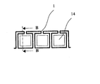
そして、インクジェット記録ヘッド用基板11の表面の端部には複数の発熱素子にそれぞれ電気的に接続された複数の電極パッド14が配置されている。この電極パッド14の近くに、インクを検知するための検知電極1としての金属配線が設けられている。
A plurality of
ここで、インクを検知するための検知電極1は上層を保護膜で被覆されていない金属配線である。また、図中の符号15で示す点線部は、電極パッド14と電極リードとが接続された後に封止樹脂によって被覆保護される領域である。
Here, the
図2は図1のA−A断面図である。この図に示すように、インクジェット記録ヘッド用基板11の基材であるSi基板31上に発熱素子(不図示)が外部の配線と電気的に接続するための電気配線32が作製されている。そして、この電気配線32と同層に、インクを検知するための検知電極1である金属配線が、成膜フォトリソグラフィ工程によって電気配線32と同工程で作製される。
2 is a cross-sectional view taken along the line AA in FIG. As shown in this figure, an
さらに、電気配線32および検知電極1を覆うようにSi基板31上に保護膜33が積層される。そして、電気配線32の上の保護膜を開口して電極パッド14を形成すると共に、インクを検知するための検知電極1としての金属配線上の保護膜を開口して露出させることにより、インクジェット記録ヘッド用基板11が完成する。
Further, a
このように、検知電極1としての金属配線は電気配線32と同工程で作り込まれている。
Thus, the metal wiring as the
検知電極1としての金属配線の材質としては、電気配線32と同一の材料を使用することが好ましい。その材料の一例としてはアルミニウム単体、アルミニウムにシリコンを添加したもの、またはアルミニウムに銅を添加したものなどがあり、アルミニウムを含んだ材料が適時使用できる。これらの材料はインクに対して比較的腐食しやすい性質であるため、後述するようにインクの検知電極として適している。
As the material of the metal wiring as the
また、検知電極1としての金属配線としては、侵入してきたインクにより早期に腐食および断線させるために、配線幅は細く、また、配線膜厚は薄くすることが望ましい。配線幅としては例えば1μm〜10μm、配線膜厚としては発熱素子用の電気配線の配線抵抗などを考慮して例えば50nm〜500nmの範囲において、要求される仕様やプロセスの条件などにより適時選択することが出来る。
In addition, it is desirable that the metal wiring as the
ここで、インクを検知するための検知電極1としての金属配線と、保護膜33の開口とについて更に詳しく述べる。
Here, the metal wiring as the
一般に、電極パッド部の開口サイズの場合は、図3に示されるように電気配線32の幅(Wd1)よりも電極パッド14の保護膜33の開口部の幅(Wh1)を小さくする(Wd1>Wh1)ことが知られている。これは保護膜33により、電極パッド部をインク等の液体から確実に保護するためである。
In general, in the case of the opening size of the electrode pad portion, as shown in FIG. 3, the width (Wh1) of the opening portion of the
これに対し、インクを検知するための検知電極1を露出する開口は図4の様になっている。すなわち、検知電極1である金属配線の幅(Wd2)より保護膜33の開口部の幅(Wh2)が大きくなる(Wd2<Wh2)ように、寸法が設定されている。
On the other hand, the opening for exposing the
このように形成することにより、インクを検知するための金属配線が保護膜33より完全にむき出し状態になっている。
By forming in this way, the metal wiring for detecting the ink is completely exposed from the
これは、インクが侵入してきたときの腐食および断線を起こりやすくするためでありインク侵入の検知感度を高めている構造である。 This is a structure that increases the sensitivity of ink intrusion detection in order to easily cause corrosion and disconnection when ink enters.
また検知電極1と保護膜33との間に隙間が形成されている。これにより、仮にインクが流れ出たときにこの隙間の毛管力によりインクが保持されることで、検知電極が腐食し易くなり、その結果断線が起こり易くなり検知精度が高まる。
A gap is formed between the
このように、インクを検知するための検知電極1の金属配線に対する開口寸法は、通常の電極パッドなどの開口寸法を決める際の考え方とは根本的に異なるものである。
As described above, the opening size of the
この金属配線の接続回路の一例を図5に示す。電極パッド14の周辺に金属配線からなる検知電極1が配置され、その金属配線の一方の端部は論理回路21に接続されている。さらに、その金属配線の他方の端部は吐出エネルギー発生用発熱素子を駆動するためのロジック回路22及びロジック回路用電源23に分岐接続されている。
An example of this metal wiring connection circuit is shown in FIG. The
このように構成することにより、電源供給用の電極パッドを追加することなく金属配線の検知電極1への電源供給が可能であり、ひいてはインクジェット記録ヘッド用基板を大きくする必要が無い。
With this configuration, it is possible to supply power to the
本実施例において論理回路21は、論理積を演算するAND回路であり、2系統の金属配線からの入力が入っている。しかしこれに限定するものではなく適時3系統、4系統など選択できる。
In this embodiment, the
正常時には論理回路21には電源からの電位供給によりハイレベルの信号が入力され、その結果ハイレベル信号が出力される。これに対し、金属配線の検知電極1にインクが侵入してくると、検知電極1の上層が保護膜により被覆されていないためにインクにより金属配線の検知電極1が腐食および断線する。
When the circuit is normal, a high level signal is input to the
そのため、論理回路21には電源からの電位供給が無くなり、プルダウン抵抗によりGND電位に落とされ、ローレベルの信号が入力し、その結果ローレベルの信号が出力されることになる。
For this reason, the
このように構成することにより、電極パッド部周辺のインク侵入を検知することが可能となる。 With this configuration, it is possible to detect ink intrusion around the electrode pad portion.
インクの侵入を検知した信号をインクジェット記録装置に知らせる方法としては色々あるが、専用の出力用の電極パッドを設ける方法が最も簡単な方法である。 There are various methods for notifying the ink jet recording apparatus of a signal that detects the intrusion of ink, but the simplest method is to provide a dedicated electrode pad for output.
なお、図9に示すように、本実施例のインクジェット記録ヘッド用基板11の複数の電極パッド14と、フレキシブルフィルム配線基板71に設けられた複数の電極リード72とが、例えばTAB技術等によって電気的に接続される。これによりインクジェット記録素子ユニット73が出来る。
As shown in FIG. 9, the plurality of
インクジェット記録素子ユニット73は、記録装置との接続に用いられるコンタクトパッド74を有する。また、図9中に符号15で示される点線部は、電極パッド14と電極リード72とが接続された後に封止樹脂の塗布によって被覆保護される領域である。
The ink jet
その後、図10に示すように、インクタンク81上に記録素子ユニット73が貼り付けられる。そして、記録素子ユニット73内の電極パッドと電極リードとの電気的接続部を、インクによる腐食や外部からの力による断線から保護するために、接続部全体を封止樹脂82によって被覆保護しインクジェット記録ヘッド83が完成する。コンタクトパッド74はインクジェット記録ヘッド83とインクジェット記録装置との接続に用いられる。
Thereafter, as shown in FIG. 10, the
さらに、本実施例のインクジェット記録ヘッド83を用いたインクジェット記録装置は、図11に示されるように構成される。すなわち、紙などの記録媒体の搬送を行う紙送り機構が記録装置本体のメインフレーム92に設けられている。さらに、メインフレーム92には、インクジェット記録ヘッド83を搭載し紙の搬送方向と交差する(好ましくは直交する)方向に往復移動するキャリッジ93が備えられている。
Furthermore, the ink jet recording apparatus using the ink
ここでは、キャリッジ93上に搭載されるインクジェット記録ヘッド83の形態が、記録ヘッドとインクカートリッジを一体化したインクジェット記録ヘッドの一例を示している。
Here, the form of the ink
しかし、インクジェット記録ヘッドとインクカートリッジが分離型の場合には、インクカートリッジは交換可能な構成とされ、インクジェット記録ヘッドはキャリッジ上に固定される構成あるいはキャリッジに対して着脱可能な構成のいずれかを適時採用される。 However, when the ink jet recording head and the ink cartridge are separated, the ink cartridge is replaceable, and the ink jet recording head is either fixed on the carriage or removable from the carriage. Adopted in a timely manner.
(実施例2)
インクを検知するための検知電極として他の実施例を図12を用いて述べる。図12では、インクを検知するための検知電極の断面構造として2層構成となっており、検知電極の上層部2の幅と下層部3との幅を比較して下層部3の幅の方が小さいことが特徴である。このような断面構造にすることにより侵入してきたインクが検知電極の上層部2に対して上面、側面、下面の3方向から腐食が進行させることができ、より検知感度を高められる点で好ましい。
(Example 2)
Another embodiment of the detection electrode for detecting ink will be described with reference to FIG. In FIG. 12, the cross-sectional structure of the detection electrode for detecting ink has a two-layer structure, and the width of the
検知電極の上層部2としては、上述した実施例で説明した電気配線32と同一の材料を使用することができる。その材料の一例としてはアルミニウム単体、アルミニウムにシリコンを添加したもの、またはアルミニウムに銅を添加したものなどがあり、アルミニウムを含んだ材料が適時使用できる。これらの材料はインクに対して腐食しやすい性質であることが知られておりインクの検知電極として適している。
As the
また、検知電極の上層部2がさらに多層(複数層)になっていても良く、例えば、アルミニウムを含んだ材料と密着向上のための材料であるTi、Crなどからなる多層構成とすることができる。また、検知電極の下層部3としては、発熱素子と同一の材料を使用することができ、TaSiNやTaNなどを適時使用できる。
Further, the
このように検知電極の上層部2を電気配線と同一の材料で構成し、下層部3を発熱素子と同一材料により構成することにより、上層部のシート抵抗を下層部のシート抵抗よりも低くすることができる。これによりシート抵抗が低い上層部がよりインクに対して腐食しやすくなり、腐食した時の抵抗値変化量が大きくなり検知感度を高められる点で好ましい。
In this way, the
次に、この検知電極の断面構造を作製する工程について図13を用いて説明する。簡略化のため、検知電極の周辺部に特化して説明を行う。 Next, a process for producing a cross-sectional structure of the detection electrode will be described with reference to FIG. For the sake of simplification, description will be made with a special focus on the periphery of the detection electrode.
まず図13(a)に示すように、Si基板31上に検知電極の下層部3としてTaSiN、および上層部2として銅添加アルミニウムをスパッタリング法により順次積層する。
First, as shown in FIG. 13A, TaSiN as the
次に、図13(b)のように、フォトリソ技術により検知電極の上層部2と下層部3を所定のパターンにパターニングする。
Next, as shown in FIG. 13B, the
その後、図13(c)のように、保護膜33としてSiNをパターニングされた検知電極を覆うようにCVD法により成膜する。
Thereafter, as shown in FIG. 13C, a
最後に図13(d)に示すように、検知電極が開口するような位置にフォトリソ技術によりレジスト(不図示)をパターニングし、ドライエッチング技術により保護膜33をエッチングし開口させる。ここで、保護膜33をエッチングする時のオーバーエッチング時に検知電極の下層部3を同時にエッチングする。
Finally, as shown in FIG. 13D, a resist (not shown) is patterned by a photolithography technique at a position where the detection electrode is opened, and the
このように検知電極の下層部としてTaSiNを、保護膜としてSiNを用いることにより、下層部の組成は、保護膜の組成の少なくとも1元素以上同じものを含んでいる。こうすることにより、保護膜のエッチング時における検知電極の上層部の材料のエッチング速度よりも下層部の材料のエッチング速度を速くすることが可能となり、上層部の幅よりも下層部の幅の方を狭く作製できる。 Thus, by using TaSiN as the lower layer portion of the detection electrode and SiN as the protective film, the composition of the lower layer portion includes at least one element that is the same as the composition of the protective film. In this way, the etching rate of the lower layer material can be made faster than the etching rate of the upper layer material of the detection electrode during etching of the protective film, and the lower layer width is larger than the upper layer width. Can be made narrow.
(実施例3)
電極パッド部周辺のインクの侵入を検知した信号をインクジェット記録装置に知らせる方法としての他の実施例を述べる。
(Example 3)
Another embodiment will be described as a method for notifying an ink jet recording apparatus of a signal that detects the intrusion of ink around the electrode pad portion.
インクジェット記録装置にインクジェット記録ヘッドを搭載するときの電気接続部の接続状態を確認するための接続状態出力回路が設けられている場合などは、この回路を利用することにより、新たな出力用電極パッドを設ける必要が無くて済む。この結果、インクジェット記録ヘッド用基板を大きくする必要が無い。 When a connection state output circuit for confirming the connection state of the electrical connection portion when mounting the ink jet recording head on the ink jet recording apparatus is provided, a new output electrode pad can be obtained by using this circuit. Need not be provided. As a result, there is no need to enlarge the inkjet recording head substrate.
このような構成では、論理回路からの出力信号を接続状態出力回路の入力側に接続して入力することにより、インク侵入の検知信号により、接続状態出力回路からの出力信号を変化させることが出来、インクジェット記録装置側への信号伝達が可能となる。 In such a configuration, by connecting the output signal from the logic circuit to the input side of the connection status output circuit and inputting it, the output signal from the connection status output circuit can be changed by the detection signal of ink intrusion. Thus, signal transmission to the ink jet recording apparatus side becomes possible.
(実施例4)
インクを検知するための検知電極の配置について他の実施例を図6を用いて述べる。
Example 4
Another embodiment of the arrangement of the detection electrodes for detecting ink will be described with reference to FIG.
本実施例では図6に示すように、電極パッド14の各々の周囲(例えば四方)を囲むように、検知電極1である金属配線が配されている。このように配置することにより、電極パッド14に対してインクがあらゆる方向から侵入してきても、インクの侵入を検知することが可能となる。
In the present embodiment, as shown in FIG. 6, metal wiring that is the
図7は図6のB−B断面図である。 7 is a cross-sectional view taken along line BB in FIG.
発熱素子を外部の配線と電気的に接続するための電気配線が、第1の電気配線51と第2の電気配線53に多層配線化されている。
The electrical wiring for electrically connecting the heat generating element to the external wiring is formed into a multilayer wiring in the first
インクジェット記録ヘッド用基板11の基材であるSi基板31上に第1の電気配線51が積層され、第1の電気配線51上に層間絶縁膜52が積層されている。さらに、この上層に、第2の電気配線53と、インクを検知するための検知電極1である金属配線とが、成膜フォトリソグラフィ工程によって同時に作製される。
A first
第1の電気配線51と第2の電気配線53とは層間絶縁膜52の開口部を通して電気的に接続されている。
The first
さらに、第2の電気配線53および検知電極1を覆うようにSi基板31上に保護膜33が積層される。そして、第2の電気配線53の上の保護膜を開口して電極パッド14を形成すると共に、インクを検知するための検知電極1としての金属配線上の保護膜を開口して露出させる。これにより、インクジェット記録ヘッド用基板11が完成する。
Further, a
以上の各実施例のような本発明は、電極パッド封止部にインクが侵入してきたときに、保護膜で被覆されていない金属配線からなる検知電極1がインクにより腐食および断線することにより、インクの侵入を検知することが出来る。そして、当該インク侵入をインクジェット記録装置へ知らせることにより、即座に印字信号および発熱素子への電力供給を停止することが出来る。
The present invention as in each of the above embodiments, when the ink has entered the electrode pad sealing portion, the
1 インクを検知するための検知電極としての金属配線
2 インクを検知するための検知電極としての金属配線の上層部
3 インクを検知するための検知電極としての金属配線の下層部
11 インクジェット記録ヘッド用基板
14 電極パッド
15 封止樹脂によって被覆保護される領域
32 電気配線
33 保護膜
71 フレキシブルフィルム配線基板
72 電極リード
82 封止樹脂
DESCRIPTION OF
Claims (13)
フレキシブルフィルム配線基板に設けられた電極リードと前記素子とを電気的に接続する電気配線と、
前記電気配線を保護する保護膜と、
前記電極リードを接合するため前記電気配線の上の前記保護膜を開口してなる電極パッドと、
前記電極パッドと前記電極リードとの電気接合部を保護するための封止樹脂が塗布される領域と、を有するインクジェット記録ヘッド用基板において、
前記封止樹脂が塗布される領域に、インクを検知するための検知電極が設けられており、
前記検知電極は、前記保護膜から露出される金属配線で形成されており、
前記保護膜の、前記金属配線を露出するための開口の幅よりも、前記金属配線の幅が狭いことを特徴とするインクジェット記録ヘッド用基板。 An element that generates energy for ejecting ink;
An electrical wiring electrically connecting the electrode lead and the element provided on the flexible film wiring board;
A protective film for protecting the electrical wiring;
An electrode pad formed by opening the protective film on the electrical wiring to join the electrode lead;
In a substrate for an ink jet recording head having a region to which a sealing resin for protecting an electrical joint portion between the electrode pad and the electrode lead is applied,
A detection electrode for detecting ink is provided in the region where the sealing resin is applied,
The detection electrode is formed of a metal wiring exposed from the protective film,
A substrate for an ink jet recording head, wherein the width of the metal wiring is narrower than the width of the opening for exposing the metal wiring in the protective film.
前記電極パッドと前記電極リードとの電気接合部を保護するための封止樹脂が塗布される領域に、上層部と下層部との複数層からなる金属配線を形成する工程と、
前記金属配線をエッチングすることにより前記上層部の幅より前記下層部の幅の方が小さい金属配線を形成工程と、を含むことを特徴とするインクジェット記録ヘッド用基板の製造方法。 An element that generates energy for ejecting ink; an electrode lead that is provided on a flexible film wiring board; and an electrical wiring that electrically connects the element; a protective film that protects the electrical wiring; and the electrode lead In the manufacturing method of a substrate for an ink jet recording head, comprising: an electrode pad formed by opening the protective film on the electrical wiring for bonding; and a detection electrode formed of a metal wiring for detecting ink.
Forming a metal wiring composed of a plurality of layers of an upper layer portion and a lower layer portion in a region where a sealing resin for protecting an electrical joint portion between the electrode pad and the electrode lead is applied;
Etching the metal wiring to form a metal wiring in which the width of the lower layer portion is smaller than the width of the upper layer portion.
Priority Applications (2)
| Application Number | Priority Date | Filing Date | Title |
|---|---|---|---|
| JP2009030896A JP5202373B2 (en) | 2008-06-16 | 2009-02-13 | Inkjet recording head substrate, inkjet recording head substrate manufacturing method, inkjet recording head, and inkjet recording apparatus |
| US12/484,649 US8246147B2 (en) | 2008-06-16 | 2009-06-15 | Inkjet printhead substrate, method for manufacturing inkjet printhead substrate, inkjet print head, and inkjet recording apparatus |
Applications Claiming Priority (3)
| Application Number | Priority Date | Filing Date | Title |
|---|---|---|---|
| JP2008156635 | 2008-06-16 | ||
| JP2008156635 | 2008-06-16 | ||
| JP2009030896A JP5202373B2 (en) | 2008-06-16 | 2009-02-13 | Inkjet recording head substrate, inkjet recording head substrate manufacturing method, inkjet recording head, and inkjet recording apparatus |
Publications (3)
| Publication Number | Publication Date |
|---|---|
| JP2010023480A true JP2010023480A (en) | 2010-02-04 |
| JP2010023480A5 JP2010023480A5 (en) | 2012-03-15 |
| JP5202373B2 JP5202373B2 (en) | 2013-06-05 |
Family
ID=41414350
Family Applications (1)
| Application Number | Title | Priority Date | Filing Date |
|---|---|---|---|
| JP2009030896A Active JP5202373B2 (en) | 2008-06-16 | 2009-02-13 | Inkjet recording head substrate, inkjet recording head substrate manufacturing method, inkjet recording head, and inkjet recording apparatus |
Country Status (2)
| Country | Link |
|---|---|
| US (1) | US8246147B2 (en) |
| JP (1) | JP5202373B2 (en) |
Cited By (4)
| Publication number | Priority date | Publication date | Assignee | Title |
|---|---|---|---|---|
| JP2011167976A (en) * | 2010-02-19 | 2011-09-01 | Brother Industries Ltd | Piezoelectric actuator, and liquid droplet discharging head |
| JP2012000921A (en) * | 2010-06-18 | 2012-01-05 | Canon Inc | Substrate for liquid discharge head and liquid discharge head |
| US8927874B2 (en) | 2011-03-28 | 2015-01-06 | Brother Kogyo Kabushiki Kaisha | Flexible wiring substrate, method for assembling flexible wiring substrate, and method for manufacturing liquid jetting apparatus |
| US11820141B2 (en) | 2020-12-14 | 2023-11-21 | Canon Kabushiki Kaisha | Element substrate, liquid ejection head, liquid ejection apparatus, and manufacturing method |
Families Citing this family (3)
| Publication number | Priority date | Publication date | Assignee | Title |
|---|---|---|---|---|
| JP5300697B2 (en) * | 2008-12-17 | 2013-09-25 | キヤノン株式会社 | Substrate for liquid discharge head and liquid discharge head |
| JP5817445B2 (en) * | 2010-11-19 | 2015-11-18 | セイコーエプソン株式会社 | Circuit board |
| US10173420B2 (en) | 2015-07-30 | 2019-01-08 | Hewlett-Packard Development Company, L.P. | Printhead assembly |
Citations (6)
| Publication number | Priority date | Publication date | Assignee | Title |
|---|---|---|---|---|
| JPH10193588A (en) * | 1997-01-10 | 1998-07-28 | Canon Inc | Ink jet recording head, recorder using the head and ink leakage sensing method |
| JP2001301132A (en) * | 2000-04-20 | 2001-10-30 | Seiko Epson Corp | Ink container, ink jet recorder using it, and ink jet recording system comprising them |
| US20020003551A1 (en) * | 1998-09-01 | 2002-01-10 | Hewlett-Packard Company | Ink leakage detecting apparatus |
| JP2006159831A (en) * | 2004-12-10 | 2006-06-22 | Canon Inc | Flexible wiring board and its production process, and ink jet recording head |
| JP2008149573A (en) * | 2006-12-18 | 2008-07-03 | Canon Inc | Ink-jet recording head and ink-jet recording device |
| JP4822353B2 (en) * | 2006-03-09 | 2011-11-24 | キヤノン株式会社 | Liquid discharge head and manufacturing method thereof |
Family Cites Families (2)
| Publication number | Priority date | Publication date | Assignee | Title |
|---|---|---|---|---|
| JPH0760954A (en) | 1993-08-30 | 1995-03-07 | Canon Inc | Ink jet recorder |
| US8438729B2 (en) * | 2006-03-09 | 2013-05-14 | Canon Kabushiki Kaisha | Method of producing liquid discharge head |
-
2009
- 2009-02-13 JP JP2009030896A patent/JP5202373B2/en active Active
- 2009-06-15 US US12/484,649 patent/US8246147B2/en active Active
Patent Citations (6)
| Publication number | Priority date | Publication date | Assignee | Title |
|---|---|---|---|---|
| JPH10193588A (en) * | 1997-01-10 | 1998-07-28 | Canon Inc | Ink jet recording head, recorder using the head and ink leakage sensing method |
| US20020003551A1 (en) * | 1998-09-01 | 2002-01-10 | Hewlett-Packard Company | Ink leakage detecting apparatus |
| JP2001301132A (en) * | 2000-04-20 | 2001-10-30 | Seiko Epson Corp | Ink container, ink jet recorder using it, and ink jet recording system comprising them |
| JP2006159831A (en) * | 2004-12-10 | 2006-06-22 | Canon Inc | Flexible wiring board and its production process, and ink jet recording head |
| JP4822353B2 (en) * | 2006-03-09 | 2011-11-24 | キヤノン株式会社 | Liquid discharge head and manufacturing method thereof |
| JP2008149573A (en) * | 2006-12-18 | 2008-07-03 | Canon Inc | Ink-jet recording head and ink-jet recording device |
Cited By (4)
| Publication number | Priority date | Publication date | Assignee | Title |
|---|---|---|---|---|
| JP2011167976A (en) * | 2010-02-19 | 2011-09-01 | Brother Industries Ltd | Piezoelectric actuator, and liquid droplet discharging head |
| JP2012000921A (en) * | 2010-06-18 | 2012-01-05 | Canon Inc | Substrate for liquid discharge head and liquid discharge head |
| US8927874B2 (en) | 2011-03-28 | 2015-01-06 | Brother Kogyo Kabushiki Kaisha | Flexible wiring substrate, method for assembling flexible wiring substrate, and method for manufacturing liquid jetting apparatus |
| US11820141B2 (en) | 2020-12-14 | 2023-11-21 | Canon Kabushiki Kaisha | Element substrate, liquid ejection head, liquid ejection apparatus, and manufacturing method |
Also Published As
| Publication number | Publication date |
|---|---|
| US8246147B2 (en) | 2012-08-21 |
| US20090309930A1 (en) | 2009-12-17 |
| JP5202373B2 (en) | 2013-06-05 |
Similar Documents
| Publication | Publication Date | Title |
|---|---|---|
| JP5202373B2 (en) | Inkjet recording head substrate, inkjet recording head substrate manufacturing method, inkjet recording head, and inkjet recording apparatus | |
| TWI551470B (en) | Printhead, print cartridge and print bar | |
| US7137685B2 (en) | Print head | |
| JP5393596B2 (en) | Inkjet recording device | |
| JP5106601B2 (en) | Method for manufacturing liquid discharge head substrate, method for manufacturing liquid discharge head, and method for inspecting liquid discharge head substrate | |
| JP4861684B2 (en) | Droplet ejector and droplet ejector forming method | |
| JP5677109B2 (en) | Inkjet recording head substrate, inkjet recording head, and recording apparatus | |
| JP2006326972A (en) | Substrate for inkjet recording head and inkjet recording head having the same | |
| JP2005161710A (en) | Inkjet recording head | |
| KR20100026998A (en) | Liquid-discharge-head substrate, method of manufacturing the same, and liquid discharge head | |
| JP5208247B2 (en) | Inkjet recording head | |
| JP2008074045A (en) | Inkjet recording head and its manufacturing method | |
| JP7112287B2 (en) | ELEMENT SUBSTRATE, PRINT HEAD, PRINTING APPARATUS, AND METHOD FOR MANUFACTURING ELEMENT SUBSTRATE | |
| JP4274554B2 (en) | Element substrate and method for forming liquid ejection element | |
| US11820141B2 (en) | Element substrate, liquid ejection head, liquid ejection apparatus, and manufacturing method | |
| JP5171377B2 (en) | Circuit board and liquid ejection device | |
| JP7465096B2 (en) | Element substrate, liquid ejection head, and recording apparatus | |
| JP2007320116A (en) | Inkjet recording head, and recording device using it | |
| JP2007062259A (en) | Head module, liquid delivering head, liquid delivering apparatus and method for manufacturing head module | |
| US10994532B2 (en) | Liquid discharge apparatus and control method thereof | |
| US10322578B2 (en) | Liquid ejection head and liquid ejection apparatus | |
| JP5317671B2 (en) | Substrate for liquid discharge head, liquid discharge head, and liquid discharge apparatus | |
| JP2021187121A (en) | Element substrate, liquid discharge head, and recording device | |
| JP2021187064A (en) | Recording element substrate, recording head, and recording device | |
| JP2022160188A (en) | Liquid discharge head substrate and recording apparatus |
Legal Events
| Date | Code | Title | Description |
|---|---|---|---|
| A521 | Request for written amendment filed |
Free format text: JAPANESE INTERMEDIATE CODE: A523 Effective date: 20120130 |
|
| A621 | Written request for application examination |
Free format text: JAPANESE INTERMEDIATE CODE: A621 Effective date: 20120130 |
|
| A977 | Report on retrieval |
Free format text: JAPANESE INTERMEDIATE CODE: A971007 Effective date: 20121228 |
|
| TRDD | Decision of grant or rejection written | ||
| A01 | Written decision to grant a patent or to grant a registration (utility model) |
Free format text: JAPANESE INTERMEDIATE CODE: A01 Effective date: 20130115 |
|
| A61 | First payment of annual fees (during grant procedure) |
Free format text: JAPANESE INTERMEDIATE CODE: A61 Effective date: 20130212 |
|
| R151 | Written notification of patent or utility model registration |
Ref document number: 5202373 Country of ref document: JP Free format text: JAPANESE INTERMEDIATE CODE: R151 |
|
| FPAY | Renewal fee payment (event date is renewal date of database) |
Free format text: PAYMENT UNTIL: 20160222 Year of fee payment: 3 |