JP2010020198A - Image display apparatus - Google Patents
Image display apparatus Download PDFInfo
- Publication number
- JP2010020198A JP2010020198A JP2008182229A JP2008182229A JP2010020198A JP 2010020198 A JP2010020198 A JP 2010020198A JP 2008182229 A JP2008182229 A JP 2008182229A JP 2008182229 A JP2008182229 A JP 2008182229A JP 2010020198 A JP2010020198 A JP 2010020198A
- Authority
- JP
- Japan
- Prior art keywords
- display device
- image display
- pdp
- cooling liquid
- groove
- Prior art date
- Legal status (The legal status is an assumption and is not a legal conclusion. Google has not performed a legal analysis and makes no representation as to the accuracy of the status listed.)
- Pending
Links
Images


Classifications
-
- H—ELECTRICITY
- H01—ELECTRIC ELEMENTS
- H01J—ELECTRIC DISCHARGE TUBES OR DISCHARGE LAMPS
- H01J11/00—Gas-filled discharge tubes with alternating current induction of the discharge, e.g. alternating current plasma display panels [AC-PDP]; Gas-filled discharge tubes without any main electrode inside the vessel; Gas-filled discharge tubes with at least one main electrode outside the vessel
- H01J11/10—AC-PDPs with at least one main electrode being out of contact with the plasma
-
- H—ELECTRICITY
- H05—ELECTRIC TECHNIQUES NOT OTHERWISE PROVIDED FOR
- H05K—PRINTED CIRCUITS; CASINGS OR CONSTRUCTIONAL DETAILS OF ELECTRIC APPARATUS; MANUFACTURE OF ASSEMBLAGES OF ELECTRICAL COMPONENTS
- H05K7/00—Constructional details common to different types of electric apparatus
- H05K7/20—Modifications to facilitate cooling, ventilating, or heating
- H05K7/20954—Modifications to facilitate cooling, ventilating, or heating for display panels
- H05K7/2099—Liquid coolant with phase change
-
- H—ELECTRICITY
- H01—ELECTRIC ELEMENTS
- H01J—ELECTRIC DISCHARGE TUBES OR DISCHARGE LAMPS
- H01J2211/00—Plasma display panels with alternate current induction of the discharge, e.g. AC-PDPs
- H01J2211/20—Constructional details
- H01J2211/66—Cooling arrangements
Abstract
Description
本発明は、テレビ映像等を表示する画像表示装置、特にその表示デバイスの放熱構造に関するものである。 The present invention relates to an image display device that displays a television image or the like, and more particularly to a heat dissipation structure of the display device.
従来の画像表示装置において、表示デバイスであるプラズマディスプレイパネルとシャーシの間に、冷却ファンを使って空気を流し、表示デバイスの温度を低減する構造が提案されている(例えば特許文献1)。
しかしながら、従来の画像表示装置においては、表示デバイスから空気への熱伝達が不十分なため、表示デバイスの温度が高くなるという課題があった。 However, the conventional image display apparatus has a problem that the temperature of the display device becomes high because heat transfer from the display device to the air is insufficient.
本発明は、表示デバイスからの熱の放出を増大することができ、表示デバイスの温度を効果的に低減可能な画像表示装置を提供することを目的とする。 It is an object of the present invention to provide an image display apparatus that can increase the release of heat from a display device and can effectively reduce the temperature of the display device.
上記目的は以下の画像表示装置により達成できる。当該課題を達成するための画像表示装置は、画像を表示する表示デバイスを備えた画像表示装置であって、前記表示デバイスの背面に複数の溝部が設けられていることを特徴とする。 The above object can be achieved by the following image display apparatus. An image display device for achieving the object is an image display device including a display device for displaying an image, and is characterized in that a plurality of grooves are provided on the back surface of the display device.
本発明による画像表示装置によれば、表示デバイスの熱の放出を増大することができ、効果的に表示デバイスの温度を低減可能である。 According to the image display apparatus of the present invention, the heat release of the display device can be increased, and the temperature of the display device can be effectively reduced.
以下、画像表示装置等の実施形態について図面を参照して説明する。なお、実施の形態において同様の動作を行う構成要素に同じ符号を付し、再度の説明を省略する場合がある。 Hereinafter, embodiments of an image display device and the like will be described with reference to the drawings. In the embodiment, components that perform the same operation may be denoted by the same reference numerals and the description thereof may be omitted.
(実施の形態1)
(1−1)構成
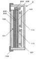
図1、2、3を用いて、実施の形態1に係る画像表示装置1の説明を行う。図1は、画像表示装置の水平方向中央位置における縦断面図である。図2は、画像表示装置の鉛直方向中央位置における横断面図である。図3は、伝熱シート、シャーシ、回路基板およびバックカバーを取除いた状態での画像表示装置の背面図である。
(Embodiment 1)
(1-1) Configuration The
なお、水平方向とは、画像表示装置の通常の設置状態における水平方向を意味する。通常は、画像表示装置の画像表示領域の長辺方向と水平方向とは平行である。また、鉛直方向とは、画像表示装置の通常の設置状態における垂直方向を意味する。通常は、画像表示装置の画像表示領域の短辺方向と垂直方向とは平行である。また、水平方向を横方向ともいい、鉛直方向を縦方向ともいう。さらに、画像表示装置の画像を表示する方向を前方といい、その反対側を後方という。また、各構成の前方の面を前面といい、後方の面を背面という。 The horizontal direction means a horizontal direction in a normal installation state of the image display device. Usually, the long side direction and the horizontal direction of the image display area of the image display apparatus are parallel to each other. The vertical direction means a vertical direction in a normal installation state of the image display device. Usually, the short side direction and the vertical direction of the image display area of the image display device are parallel to each other. The horizontal direction is also referred to as the horizontal direction, and the vertical direction is also referred to as the vertical direction. Furthermore, the direction in which the image of the image display device is displayed is referred to as the front, and the opposite side is referred to as the rear. The front surface of each component is referred to as the front surface, and the rear surface is referred to as the back surface.
画像表示装置1は、プラズマディスプレイパネル(以下、PDPともいう。)101、シャーシ105、フロントカバー106、バックカバー107、前面フィルター108、空冷ファン109、伝熱シート113、回路基板114を具備する。PDP101は表示デバイスの一例である。
The
PDP101は、前面ガラス基板111と、背面ガラス基板112とを有する。前面ガラス基板111は、第1の方向と平行な走査電極と維持電極とからなる表示電極対が多数形成されている。背面ガラス基板112は、第1の方向と交差する第2の方向と平行なアドレス電極が多数形成されている。表示電極対は誘電体層で覆われている。誘電体層は、MgO等で形成された保護で覆われている。また、背面ガラス基板112は、赤・青・緑の蛍光体が塗布されている。前面ガラス基板111と背面ガラス基板112とは貼り合わされている。前面ガラス基板111および背面ガラス基板112の最も広い面は長方形である。第1の方向は長方形の長辺方向であり、一般に水平方向になるようにして設置される。第2の方向は長方形の短辺方向であり、一般に鉛直方向になるようにして設置される。前面ガラス基板111および背面ガラス基板112はそれぞれおよそ1.5mm〜3mmの厚さである。
The PDP 101 includes a
前面から見て表示電極対とアドレス電極とが交わる位置であって、表示電極対とアドレス電極とに挟まれた部分を放電セルという。放電セルには赤・青・緑のいずれかの蛍光体が塗布されている。放電セルにはヘリウム(He)、ネオン(Ne)、キセノン(Xe)等の希ガスを含む放電ガスが封入されている。そして表示電極対およびアドレス電極に電圧を印加して放電セルに放電を起こし、紫外線を発生させる。そして、発生した紫外線で蛍光体を刺激して発光させ画像を表示する。 A portion where the display electrode pair and the address electrode intersect when viewed from the front surface and is sandwiched between the display electrode pair and the address electrode is called a discharge cell. One of red, blue, and green phosphors is applied to the discharge cell. A discharge gas containing a rare gas such as helium (He), neon (Ne), or xenon (Xe) is sealed in the discharge cell. A voltage is applied to the display electrode pair and the address electrode to cause a discharge in the discharge cell, thereby generating ultraviolet rays. Then, the phosphor is stimulated with the generated ultraviolet light to emit light and an image is displayed.
具体的には、まず、走査電極の全ラインに電圧を印加して全部の放電セルで放電を起こす初期化放電を行う。次に、走査電極に順次電圧を印加するとともに、電圧が印加された走査電極上で発光させたい放電セルと交わるアドレス電極にも電圧を印加する。これをアドレス放電といい、電圧が印加された走査電極とアドレス電極とが交わる位置の放電セルが発光し、該放電セルが発光セルとして選択される。その後、走査電極と維持電極との間に交流電圧を印加する維持放電を行う。維持放電により、先程選択された発光セルのみが発光し、PDP101は画像を表示する。
Specifically, first, an initializing discharge is performed in which a voltage is applied to all lines of the scan electrode to cause discharge in all the discharge cells. Next, a voltage is sequentially applied to the scan electrodes, and a voltage is also applied to the address electrodes that intersect the discharge cells that are desired to emit light on the scan electrodes to which the voltages have been applied. This is called address discharge, and a discharge cell at a position where a scan electrode to which a voltage is applied intersects with the address electrode emits light, and the discharge cell is selected as a light emitting cell. Thereafter, a sustain discharge is performed in which an AC voltage is applied between the scan electrode and the sustain electrode. Due to the sustain discharge, only the light emitting cell selected previously emits light, and the
PDP101は、放電セルの内部で放電を発生させて画像を表示する際、PDP101自体が高温になりやすい。PDP101が高温になると、放電特性が変化して、発光すべき放電セルが発光しない、または発光すべきでない放電セルが発光する等の誤放電が発生しやすくなり、画像表示品質を低下させる問題が生じる。また、PDP101が高温になると、前面ガラス基板111または背面ガラス基板112の割れといった問題が生じる。従って、PDP101で発生する熱を効率よく逃がし、PDP101を低い温度、例えば70〜80℃に抑えることが重要である。
When the PDP 101 displays an image by generating a discharge inside the discharge cell, the
PDP101は、溝部102を具備する。具体的には、溝部102は、PDP101を構成する背面ガラス基板112のシャーシ105に対向する面に、複数形成されている。溝部102は、略鉛直方向に略平行に形成されている。溝部102は、背面ガラス基板112の下端から上端まで形成されている。また、溝部102の内壁は、サンドブラスト工法などによって粗面が形成されている。具体的には、溝部102の内壁は表面粗さが算術平均粗さ(Ra)で表すと2μmから20μm程度である。
The PDP 101 includes a
シャーシ105は、PDP101をその一方の面に保持する。
The
シャーシ105は、熱伝導率および電気伝導率の高いアルミニウム、銅等の金属板で構成されている。シャーシ105の最も広い面の大きさが前面ガラス基板111および背面ガラス基板112の最も広い面とほぼ等しく、厚みは1.5〜4mm程度である。また必要に応じて補強のための折り曲げ加工あるいは補強リブが設けられている。シャーシ105の一方の面(前面)には伝熱シート113を介してPDP101が取り付けられる。シャーシ105の他方の面(背面)には、回路基板114がシャーシ105と平行になるように取り付けられている。
The
シャーシ105は、PDP101や回路基板114が発生した熱を吸収し、空気中や他の部材に熱を逃がす放熱部材として機能する。また、シャーシ105は、PDP101や回路基板114を支持しこれらの強度を保つ強度部材としても機能する。さらに、シャーシ105は、PDP101や回路基板114等の電気的なグラウンドとしても機能する。
The
フロントカバー106は、例えば樹脂などで形成されている。フロントカバー106は、前方から見て中央部が開口した矩形状の枠体である。フロントカバー106は、前面フィルター108の周縁部を前方から覆うように構成されている。
The
バックカバー107は、金属板をプレス成形することにより形成される。バックカバー107は、PDP101の背面を覆うようにシャーシ105に固定される。バックカバー107は、回路基板114を覆うように構成される。バックカバー107は、鉛直方向下側の面に通風孔を有しており、バックカバー107の外部と内部とを空気の入れ替えが可能となっている。バックカバー107は、導電性を有し、PDP101、回路基板114等から放射される電磁波を遮蔽する。
The
前面フィルター108は、PDP101の前方に配置される。前面フィルター108は、ガラスまたはアクリルなどの樹脂で構成された矩形状の透明基板と、透明基板上に形成された種々の機能フィルムとを有する。具体的には、機能フィルムは、反射防止フィルム、着色フィルム、ネオンカットフィルム、近赤外カットフィルム、導電性フィルム等である。
The
空冷ファン109は、バックカバー107に固定して設けられる。空冷ファン109は、バックカバー107の内部から空気を強制的に排出し、バックカバー107の通風孔からバックカバー107の内部への空気の流入の効率を向上させる。なお、空冷ファン109は、バックカバーの外部から内部へ空気を強制的に流入し、バックカバーの内部から外部への空気の排出の効率を向上させるようにしてもよい。
The
空冷ファン109としては、軸流ファン、もしくは遠心ファン等を用いる。本実施の形態では空冷ファン109として遠心ファンを用いている。本実施の形態で用いた遠心ファンは、空気をファンの両側面から吸込み、ファンの上端に排出するタイプのものである。空冷ファン109は、シャーシ105に対して鉛直方向上側に設けられている。また、シャーシ105の背面よりも前方に設けられている。さらに、溝部102よりも後方に設けられている。
As the
空気は、バックカバー107の鉛直方向下側の面の通風孔からバックカバー107の内部に流入する。そして、空気は、シャーシ105と回路基板114の間を流れる(矢印A1)。また、空気は、PDP101とシャーシ105前面の間を流れる(矢印A2)。具体的には、空気は、溝部102を流れる(矢印A2)。最後に、空気は、空冷ファン109の前面および背面から吸込まれ、空冷ファン109の鉛直方向上側の面から排出される(矢印A3)。
Air flows into the
伝熱シート113は、PDP101の背面とシャーシ105の前面の間に渡って設けられている。伝熱シート113は、PDP101の背面をほぼ全面に渡って覆っている。伝熱シート113は、シリコンゴム等、熱伝導率が比較的高く、柔軟性を有する材料が一般的に用いられる。また、伝熱シート113の両面は粘着性を有しており、伝熱シート113とシャーシ105とは接着されており、伝熱シート113とPDP101とは接着されている。こうすることによって、シャーシ105はPDP101を保持する。
The
回路基板114は、画像表示をコントロールするための、SUS基板、SCAN基板、データコントロール基板、映像を受信するためのチューナー基板、映像を処理するためのデジタル信号処理基板、各部に電力を供給するための電源回路基板、等々である。SUS基板は、維持電極に対し電圧を印加する。SCAN基板は、走査電極に対し電圧を印加する。データコントロール基板は、アドレス電極に対し電圧を印加する。
The
(1−2)作用
次に、画像表示装置1の作用について説明する。
(1-2) Operation Next, the operation of the
PDP101は自発光デバイスであり、PDP101自身が発熱する。すなわち、PDP101は発熱体である。PDP101の放電によって発生した熱は、PDP101の背面ガラス基板112に伝導される。
The
背面ガラス基板112が溝部102を有していない場合、背面ガラス基板112の背面の多くの部分は空気と接触しない。そして、背面ガラス基板112の熱の大部分は伝熱シート113に伝達され、伝熱シート113からシャーシ105に伝達される。そして、シャーシ105から空気中に熱が放出される。
If the
一方、本実施の形態によれば、背面ガラス基板112が溝部102を有している。そして、溝部102の内壁は空気と接している。従って、溝部102の内壁から直接空気中に熱を放出することが可能である。従って、背面ガラス基板112が溝部102を有していない場合と比べ、PDP101の放熱効率が高い。
On the other hand, according to the present embodiment, the
また、溝部102を設けることにより、背面ガラス基板112と空気との接触面積が大きくなっており、さらに放熱効率が高い。さらには、溝部102の内部に粗面が形成されているため、背面ガラス基板112と空気との接触面積がさらに大きくなっており、さらに放熱効率が高い。
Further, the provision of the
溝部102は、略鉛直方向に略平行に形成されているため、溝部102の内部の空気は自然対流によって効率よく流れ、さらに放熱効率が高い。さらには、空冷ファン109によって強制的に溝部102の内部に空気を流しているため(矢印A2)、さらに放熱効率が高い。
Since the
また、溝部102の底面、すなわち、溝部102の最も前方に配置される面においては、より発熱源である放電部の近くから熱を奪うため、効率的な空気への熱伝達が可能となる。
Further, since heat is taken away from the vicinity of the discharge part, which is a heat generation source, on the bottom surface of the
なお、PDP101からの熱の一部は、背面ガラス基板112から伝熱シート113に伝達され、伝熱シート113からシャーシ105に伝達される。そして、シャーシ105から空気中に熱が放出される。
Part of the heat from the
回路基板114から発生した熱は、回路基板114の下側から流れてくる空気(矢印A1)に伝達される。回路基板114及びシャーシ105から熱を吸収した空気(矢印A1)は、溝部102から熱を吸収した空気(矢印A2)と空冷ファン109で合流し、バックカバー107の上面の放熱孔(図省略)から画像表示装置外部に排出される(矢印A3)。
The heat generated from the
上記構成においては、PDP101の主な放熱経路と、回路基板114の主な放熱経路を分離することによって、お互いの熱干渉を低減し、効率的なPDP101および回路基板114の放熱が可能となっている。
In the above configuration, by separating the main heat dissipation path of the
(実施の形態2)
(2−1)構成
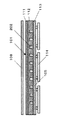
図4、5、6を用いて、実施の形態2に係る画像表示装置2を説明する。図4は、画像表示装置の水平方向中央位置における縦断面図である。図5は、画像表示装置の鉛直方向中央位置における横断面図である。図6は、画像表示装置の伝熱シート、シャーシ、回路基板およびバックカバーを取除いた状態での背面図である。
(Embodiment 2)
(2-1) Configuration The
画像表示装置2は、PDP101、冷却用液体203、ポンプ204、シャーシ105、フロントカバー106、バックカバー107、前面フィルター108、空冷ファン209、輸送管210、伝熱シート113、回路基板114を具備する。
The
PDP101は、溝部202、を具備する。具体的には、溝部202は、PDP101を構成する背面ガラス基板112のシャーシ105に対向する面に、形成されている。また、溝部202は、連続しており、屈曲した形状である。溝部202の両端は背面ガラス基板112の上端に至っている。また、溝部202の内壁は、サンドブラスト工法などによって粗面が形成されている。具体的には、溝部202の内壁は表面粗さが算術平均粗さ(Ra)で表すと2μmから20μm程度である。
The
PDP101と、シャーシ105との間には、伝熱シート113が設けられる。伝熱シート113が背面ガラス基板112の溝部202が形成された面に圧着されることによって、溝部202と伝熱シート113とで一続きの流路が形成される。そして、連続した流路の両端を除いては、機密性が保たれる。流路の内部には冷却用液体203が満たされている。
A
冷却用液体203は、エチレングリコールなどの凍結防止剤を混合した冷却用の液体である。 The cooling liquid 203 is a cooling liquid in which an antifreezing agent such as ethylene glycol is mixed.
輸送管210は、内部に冷却用液体203が満たされた管である。輸送管210は、溝部202の両端、すなわち、流路の両端に連結している。輸送管210は、ポンプ204にも連結している。流路、輸送管210、及び、ポンプ204によって、冷却用液体203の循環経路が形成される。
The
ポンプ204は、冷却用液体203を溝部202及び輸送管210の内部で循環させる。
The
空冷ファン209は、バックカバー107に固定して設けられる。空冷ファン209は、バックカバー107の外部から空気を強制的に吸入し、風を輸送管210に当てる。輸送管210に当てた風はバックカバー107の通風孔からバックカバー107の外部へ排出される。空冷ファン209としては、軸流ファン、もしくは遠心ファン等を用いる。本実施の形態では空冷ファン209として軸流ファンを用いている。
The
(2−2)作用
次に、画像表示装置2の作用について説明する。
(2-2) Operation Next, the operation of the
PDP101の放電によって発生した熱は、PDP101の背面ガラス基板112に伝導される。そして、その熱は、背面ガラス基板112から溝部202と伝熱シート113とによって構成される流路に充填された冷却用液体203に伝達される。冷却用液体203は、PDP101の背面においては、PDP101から吸熱しながら溝部202を通過する。PDP101の背面で熱を吸収した冷却用液体203は、ポンプ204によって、PDP101の外側の輸送管210に送られる。空冷ファン209が輸送管210に風、すなわち空気を当てることによって、輸送管210の表面から冷却用液体203の熱を吸収する。この結果として、冷却用液体203が冷却される。冷却された冷却用液体203は、ポンプ204によって、PDP101の背面の流路に戻る。このように冷却用液体203を循環してPDP101の熱を効率的に放熱することが可能となる。
Heat generated by the discharge of the
さらには、溝部202の内部に粗面が形成されているため、背面ガラス基板112と冷却用液体203との接触面積がさらに大きくなっており、さらに放熱効率が高い。
Furthermore, since the rough surface is formed inside the
また、PDP101の背面の流路を溝部202と伝熱シート113とによって形成しており、流路の形成が容易である。
Moreover, the flow path on the back surface of the
(実施の形態3)
(3−1)構成
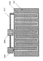
図7、8、9を用いて、実施の形態3に係る画像表示装置3について説明する。図7は、画像表示装置の水平方向中央位置における縦断面図である。図8は、画像表示装置の鉛直方向中央位置における横断面図である。図9は、画像表示装置の伝熱シート、アルミシャーシ、回路基板およびバックカバーを取除いた状態での背面図である。
(Embodiment 3)
(3-1) Configuration The
画像表示装置1は、PDP101、冷却用液体303、シャーシ105、フロントカバー106、バックカバー107、前面フィルター108、空冷ファン309、伝熱シート113、回路基板114を具備する。
The
PDP101は、溝部302を具備する。具体的には、溝部302は、PDP101を構成する背面ガラス基板112のシャーシ105に対向する面に、複数形成されている。溝部302は、略鉛直方向に略平行に配置される。溝部302は、背面ガラス基板112の上端には至っていない。また、溝部302は、背面ガラス基板112の下端には至っていない。溝部302の内壁は、サンドブラスト工法などによって粗面が形成されている。具体的には、溝部302の内壁は表面粗さが算術平均粗さ(Ra)で表すと2μmから20μm程度である。
The
PDP101と、シャーシ105との間には、伝熱シート113が設けられる。伝熱シート113が背面ガラス基板112の溝部302が形成された面に圧着されることによって、複数の管状の閉空間を形成されている。管状の閉空間は機密性が保たれている。管状の閉空間の内部には冷却用液体303と空気が減圧状態で封入されている。すなわち、閉空間の内部は大気圧よりも低い圧力となっている。
A
冷却用液体303としては、純水を用いている。他にも、フロン系のHCHC、HFC、もしくは炭化水素系のメチルアルコール、アセトン等を用いることができる。
Pure water is used as the cooling
空冷ファン309は、バックカバー107に固定して設けられる。空冷ファン309は、バックカバー107の外部から空気を強制的に吸入し、風をシャーシ105の上部に当てる。シャーシ105に当てた風はバックカバー107の通風孔からバックカバー107の外部へ排出される。空冷ファン309としては、軸流ファン、もしくは遠心ファン等を用いる。本実施の形態では空冷ファン309として軸流ファンを用いている。
The
(3−2)動作
次に、画像表示装置3の動作について説明する。
(3-2) Operation Next, the operation of the
PDP101の放電によって発生した熱は、PDP101の背面ガラス基板112に伝導される。そして、その熱は、溝部302と伝熱シート113とによって構成される閉空間に封入された冷却用液体303を蒸発させる。冷却用液体303は、液体から気体への相変化に伴う潜熱として、PDP101から熱を吸収し、PDP101の温度を低減する。蒸発した冷却用液体303は閉空間を上昇し、PDP101の上端部に到達する。PDP101の上端部には空冷ファン309が配置され、気化し上昇した高温の冷却用液体303から熱を冷却する。具体的には、気化し上昇した高温の冷却用液体303から伝熱シート113を介してシャーシ105に熱が伝わり、シャーシ105から空気中に放熱される。その結果、冷却用液体303は温度が下がって気体から液体へ相変化する。液化した冷却用液体303は、重力によって閉空間の壁面を伝って落下する。壁面を伝う冷却用液体303の一部は、閉空間の下部に到達する。また、壁面を伝う冷却用液体303の一部は、閉空間の下部に到達するまでにPDP101からの熱を吸収して気化し、再び上昇する。
Heat generated by the discharge of the
さらには、溝部302の内部に粗面が形成されているため、背面ガラス基板112と冷却用液体303との接触面積がさらに大きくなっており、さらに放熱効率が高い。また、粗面によって、重力に加え、毛細管力も使った冷却用液体303の輸送が可能となるため、更に熱輸送量を増大することが可能となる。なお、溝部302の内面に閉空間に沿った鉛直方向の溝を設けるようにしても同様の効果が得られる。また、細線ワイヤを編み合せたものを閉空間の壁面に沿って配置しても、毛細管力を利用することが可能であって、同様の効果が得られる。
Furthermore, since the rough surface is formed inside the
また、PDP101の背面の閉空間を溝部302と伝熱シート113とによって形成しており、閉空間の形成が容易である。
In addition, the closed space on the back surface of the
(実施の形態4)
(4−1)構成
図10、11、12を用いて、実施の形態4に係る画像表示装置4について説明する。図10は、画像表示装置の水平方向中央位置における縦断面図である。図11は、画像表示装置の鉛直方向中央位置における横断面図である。図12は、画像表示装置の伝熱シート、アルミシャーシ、回路基板およびバックカバーを取除いた状態での背面図である。
(Embodiment 4)
(4-1) Configuration The image display device 4 according to the fourth embodiment will be described with reference to FIGS. FIG. 10 is a vertical cross-sectional view at the horizontal center position of the image display device. FIG. 11 is a cross-sectional view of the image display device at the center position in the vertical direction. FIG. 12 is a rear view of the image display device with a heat transfer sheet, an aluminum chassis, a circuit board, and a back cover removed.
画像表示装置4は、PDP101、ポンプ204、シャーシ105、フロントカバー106、バックカバー107、前面フィルター108、空冷ファン209、輸送管210、伝熱シート113、回路基板114を具備する。
The image display device 4 includes a
PDP101は、内部に流路402を具備する。さらに、流路402に冷却用液体203を有する。具体的には、実施の形態2は、溝部202と伝熱シート113とにより流路を形成していたのに対し、本実施の形態は、PDP101を構成する背面ガラス基板112の内部に面内に沿って流路402が形成されている。また、流路402の内壁は、サンドブラスト工法などによって粗面が形成されている。具体的には、流路402の内壁は表面粗さが算術平均粗さ(Ra)で表すと2μmから20μm程度である。
The
その他の構成は、実施の形態2と実質的に同様である。すなわち、輸送管210は、流路402の両端に連結している。流路402、輸送管210、及び、ポンプ204によって、冷却用液体203の循環経路が形成される。ポンプ204は、冷却用液体203を流路402及び輸送管210の内部で循環させる。
Other configurations are substantially the same as those of the second embodiment. That is, the
(4−2)作用
次に、画像表示装置4の作用について説明する。
(4-2) Operation Next, the operation of the image display device 4 will be described.
PDP101の放電によって発生した熱は、PDP101の背面ガラス基板112に伝導される。そして、その熱は、背面ガラス基板112から流路402に充填された冷却用液体203に伝達される。冷却用液体203は、PDP101の背面においては、PDP101から吸熱しながら流路402を通過する。PDP101の背面で熱を吸収した冷却用液体203は、ポンプ204によって、PDP101の外側の輸送管210に送られる。空冷ファン209が輸送管210に風、すなわち空気を当てることによって、輸送管210の表面から冷却用液体203の熱を吸収する。この結果として、冷却用液体203が冷却される。冷却された冷却用液体203は、ポンプ204によって、PDP101の背面の流路402に戻る。このように冷却用液体203を循環してPDP101の熱を効率的に放熱することが可能となる。
Heat generated by the discharge of the
さらには、流路402の内部に粗面が形成されているため、背面ガラス基板112と冷却用液体203との接触面積がさらに大きくなっており、さらに放熱効率が高い。
Furthermore, since a rough surface is formed inside the
(実施の形態5)
(5−1)構成
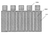
図13、14、15を用いて、実施の形態5に係る画像表示装置の説明図である。図13は、画像表示装置の水平方向中央位置における縦断面図である。図14は、画像表示装置の鉛直方向中央位置における横断面図である。図15は、画像表示装置の伝熱シート、アルミシャーシ、回路基板およびバックカバーを取除いた状態での背面図である。
(Embodiment 5)
(5-1) Configuration FIG. 13, FIG. 14, and FIG. 15 are explanatory diagrams of an image display device according to a fifth embodiment. FIG. 13 is a vertical cross-sectional view at the horizontal center position of the image display device. FIG. 14 is a cross-sectional view of the image display device at the center position in the vertical direction. FIG. 15 is a rear view of the image display device with a heat transfer sheet, an aluminum chassis, a circuit board, and a back cover removed.
画像表示装置5は、PDP101、シャーシ105、フロントカバー106、バックカバー107、前面フィルター108、空冷ファン309、伝熱シート113、回路基板114を具備する。
The image display device 5 includes a
PDP101は、流路502、を具備する。さらに、流路502に冷却用液体303を有する。冷却用液体303は減圧状態で流路502に封入されている。具体的には、流路502は、PDP101を構成する背面ガラス基板112の内部に、複数形成されている。流路502は、略鉛直方向に略平行に配置される。流路502は、背面ガラス基板112の上端には至っていない。また、流路502は、背面ガラス基板112の下端には至っていない。流路502の内壁は、粗面が形成されている。具体的には、流路502の内壁は表面粗さが算術平均粗さ(Ra)で表すと2μmから20μm程度である。
The
流路502は、複数の管状の閉空間を形成している。管状の閉空間は機密性が保たれている。管状の閉空間の内部には冷却用液体303と空気が減圧状態で封入されている。すなわち、閉空間の内部は大気圧よりも低い圧力となっている。
The
実施の形態3は、溝部302と伝熱シート113とよって、閉空間を形成しているのに対し、本実施の形態は、PDP101を構成する背面ガラス基板112の内部に面内に沿って形成した流路502が閉空間である点が異なる。
In the third embodiment, a closed space is formed by the
(5−2)作用
次に、画像表示装置の作用について説明する。
(5-2) Operation Next, the operation of the image display device will be described.
PDP101の放電によって発生した熱は、PDP101の背面ガラス基板112に伝導される。そして、その熱は、流路502に封入された冷却用液体303を蒸発させる。冷却用液体303は、液体から気体への相変化に伴う潜熱として、PDP101から熱を吸収し、PDP101の温度を低減する。蒸発した冷却用液体303は流路502を上昇し、PDP101の上端部に到達する。PDP101の上端部には空冷ファン309が配置され、気化し上昇した高温の冷却用液体303から熱を冷却する。具体的には、気化し上昇した高温の冷却用液体303から伝熱シート113を介してシャーシ105に熱が伝わり、シャーシ105から空気中に放熱される。その結果、冷却用液体303は温度が下がって気体から液体へ相変化する。液化した冷却用液体303は、重力によって流路502の壁面を伝って落下する。壁面を伝う冷却用液体303の一部は、流路502の下部に到達する。また、壁面を伝う冷却用液体303の一部は、流路502の下部に到達するまでにPDP101からの熱を吸収して気化し、再び上昇する。
Heat generated by the discharge of the
さらには、流路502の内部に粗面が形成されているため、背面ガラス基板112と冷却用液体303との接触面積がさらに大きくなっており、さらに放熱効率が高い。また、粗面によって、重力に加え、毛細管力も使った冷却用液体303の輸送が可能となるため、更に熱輸送量を増大することが可能となる。なお、流路502の内面に閉空間に沿った鉛直方向の溝を設けるようにしても同様の効果が得られる。また、細線ワイヤを編み合せたものを流路502の壁面に沿って配置しても、毛細管力を利用することが可能であって、同様の効果が得られる。
Furthermore, since a rough surface is formed in the
(その他の実施形態)
なお、上述の実施の形態では、PDP101とシャーシ105の間に、伝熱シート113を介在させているが、伝熱シートは無くても良い。実施の形態2では溝部202と他の部材、例えば、シャーシ105とによって流路を形成してもよい。また、実施の形態3では、溝部302と他の部材、例えば、シャーシ105とによって閉空間を形成してもよい。
(Other embodiments)
In the above-described embodiment, the
また、実施の形態2、4では、流路を略垂直方向に設け、PDP101の熱をPDP101の上端部に移動し、空冷ファンによって放熱しているが、流路を水平方向に設けても良い。
In the second and fourth embodiments, the flow path is provided in a substantially vertical direction and the heat of the
また、実施の形態3、5では、流路を略鉛直方向に設け、PDP101の熱をPDP101の上端部に移動し、空冷ファンによって放熱しているが、流路を水平方向に設けた場合は、PDP101の中央部の熱を左右周辺部に移動し、空冷ファンによって放熱しても良い。
In the third and fifth embodiments, the flow path is provided in a substantially vertical direction, and the heat of the
上記の各実施形態の説明においては、ファンを用いてバックカバーの内部の空気を排出する構造について説明したが、本発明はこれに限定されるものではなく、ファンを用いることなく、通風孔を通して自然対流のみで画像表示装置の内部を冷却させる構造であってもよい。 In the description of each of the above embodiments, the structure in which the air inside the back cover is discharged using a fan has been described. However, the present invention is not limited to this, and the fan is not used and the air vent is passed through. A structure in which the inside of the image display device is cooled only by natural convection may be used.
上記の各実施形態の説明においては、表示デバイスとしてプラズマディスプレイパネルを例に説明したが、液晶ディスプレイやELディスプレイ等にも適用できる。 In the description of each of the above embodiments, the plasma display panel has been described as an example of the display device, but the present invention can also be applied to a liquid crystal display, an EL display, or the like.
また、上記の各実施形態において用いた具体的な数値等は、単に一例を挙げたに過ぎず、表示デバイスの特性や画像表示装置の仕様等に合わせて、適宜最適な値に設定することが可能である。 In addition, the specific numerical values used in each of the above embodiments are merely examples, and can be appropriately set to optimum values according to the characteristics of the display device, the specifications of the image display apparatus, and the like. Is possible.
(実施の形態の特徴)
上述の実施の形態に係る画像表示装置は、画像を表示する表示デバイスを備えた画像表示装置であって、前記表示デバイスの背面に複数の溝部が設けられることを特徴とする。これにより、効果的に表示デバイス温度を低減可能である。
(Features of the embodiment)
The image display device according to the above-described embodiment is an image display device including a display device that displays an image, and is characterized in that a plurality of grooves are provided on the back surface of the display device. Thereby, the display device temperature can be effectively reduced.
上述の実施の形態に係る画像表示装置は、さらに、前記溝部は、略鉛直方向に配置されていることを特徴とする。これにより、溝内部の気流または液体の浮力による上昇を利用することができ、また、液化した冷却用液体の重力による循環を促進することができ、効果的に表示デバイス温度を低減可能である。 The image display device according to the above-described embodiment is further characterized in that the groove is arranged in a substantially vertical direction. As a result, it is possible to use the air flow inside the groove or the rise due to the buoyancy of the liquid, and it is possible to promote the circulation of the liquefied cooling liquid by the gravity, thereby effectively reducing the display device temperature.
上述の実施の形態に係る画像表示装置は、さらに、前記溝部の内部に冷却用液体を有することを特徴とする。これにより、表示デバイスからの吸熱量を増大することが可能となり、効果的に表示デバイス温度を低減可能である。 The image display device according to the above-described embodiment further includes a cooling liquid inside the groove. As a result, the amount of heat absorbed from the display device can be increased, and the display device temperature can be effectively reduced.
上述の実施の形態に係る画像表示装置は、さらに、前記冷却用液体を前記溝部の内部で循環させるポンプをさらに備える。これにより、効果的に表示デバイス温度を低減可能である。 The image display device according to the above-described embodiment further includes a pump that circulates the cooling liquid inside the groove. Thereby, the display device temperature can be effectively reduced.
上述の実施の形態に係る画像表示装置は、さらに、前記冷却用液体は前記溝部に減圧状態で封入されていることを特徴とする。これにより、表示デバイスの発熱を表示デバイス上端に輸送することができ、効果的に表示デバイス温度を低減可能である。 The image display device according to the above-described embodiment is further characterized in that the cooling liquid is sealed in the groove portion in a reduced pressure state. Thereby, the heat generated by the display device can be transported to the upper end of the display device, and the display device temperature can be effectively reduced.
上述の実施の形態に係る画像表示装置は、さらに、画像を表示する表示デバイスを備えた画像表示装置であって、前記表示デバイスの内部に流路を有し、前記流路に冷却用液体を有することを特徴とする。これによって、効果的に表示デバイス温度を低減可能である。 The image display device according to the above-described embodiment is an image display device further including a display device that displays an image, and has a flow channel inside the display device, and a cooling liquid is supplied to the flow channel. It is characterized by having. Thereby, the display device temperature can be effectively reduced.
上述の実施の形態に係る画像表示装置は、さらに、前記冷却用液体を前記流路の内部で循環させるポンプをさらに備える。これにより、表示デバイスの発熱を表示デバイスの背面から外部に輸送することができ、効果的に表示デバイス温度を低減可能である。 The image display device according to the above-described embodiment further includes a pump that circulates the cooling liquid inside the flow path. Accordingly, the heat generated by the display device can be transported from the back surface of the display device to the outside, and the display device temperature can be effectively reduced.
上述の実施の形態に係る画像表示装置は、さらに、前記冷却用液体は前記流路に減圧状態で封入されていることを特徴とする。これにより、表示デバイスの発熱を表示デバイス上端に輸送することができ、効果的に表示デバイス温度を低減可能である。 The image display device according to the above-described embodiment is further characterized in that the cooling liquid is sealed in the flow path in a reduced pressure state. Thereby, the heat generated by the display device can be transported to the upper end of the display device, and the display device temperature can be effectively reduced.
上述の実施の形態に係る画像表示装置は、さらに、前記溝部は、略鉛直方向に配置されることを特徴とする。溝内部の気流または液体の浮力による上昇を利用することができ、また、液化した冷却用液体の重力による循環を促進することができ、効果的に表示デバイス温度を低減可能である。 The image display device according to the above-described embodiment is further characterized in that the groove is arranged in a substantially vertical direction. The rise by the air flow inside the groove or the buoyancy of the liquid can be used, and the circulation of the liquefied cooling liquid by the gravity can be promoted, and the display device temperature can be effectively reduced.
(その他)
上述の実施の形態は本発明の一例である。本発明は、以上の実施の形態に限定されることなく、種々の変更が可能であり、それらも本発明の範囲内に包含されるものであることは言うまでもない。
(Other)
The above-described embodiment is an example of the present invention. The present invention is not limited to the above-described embodiments, and various modifications are possible, and it goes without saying that these are also included in the scope of the present invention.
以上のように、本発明にかかる画像表示装置は、効果的に表示デバイスの温度を低減可能であるという効果を有し、薄型大画面の画像表示装置等として有用である。 As described above, the image display device according to the present invention has an effect that the temperature of the display device can be effectively reduced, and is useful as a thin and large screen image display device.
1 画像表示装置
101 表示デバイス(PDP)
102、202、302 溝部
105 シャーシ
106 フロントカバー
107 バックカバー
108 前面フィルター
109、209、309 空冷ファン
113 伝熱シート
114 回路基板
203、303 冷却用液体
204 ポンプ
402、502 流路
DESCRIPTION OF
102, 202, 302
Claims (10)
前記表示デバイスの背面に複数の溝部が設けられていることを特徴とする画像表示装置。 An image display device including a display device for displaying an image,
An image display device, wherein a plurality of grooves are provided on the back surface of the display device.
前記表示デバイスの内部に流路を有し、前記流路に冷却用液体を有することを特徴とする画像表示装置。 An image display device including a display device for displaying an image,
An image display device comprising: a flow channel inside the display device; and a cooling liquid in the flow channel.
Priority Applications (2)
| Application Number | Priority Date | Filing Date | Title |
|---|---|---|---|
| JP2008182229A JP2010020198A (en) | 2008-07-14 | 2008-07-14 | Image display apparatus |
| US12/469,235 US20100007258A1 (en) | 2008-07-14 | 2009-05-20 | Image display apparatus |
Applications Claiming Priority (1)
| Application Number | Priority Date | Filing Date | Title |
|---|---|---|---|
| JP2008182229A JP2010020198A (en) | 2008-07-14 | 2008-07-14 | Image display apparatus |
Publications (2)
| Publication Number | Publication Date |
|---|---|
| JP2010020198A true JP2010020198A (en) | 2010-01-28 |
| JP2010020198A5 JP2010020198A5 (en) | 2011-08-18 |
Family
ID=41504546
Family Applications (1)
| Application Number | Title | Priority Date | Filing Date |
|---|---|---|---|
| JP2008182229A Pending JP2010020198A (en) | 2008-07-14 | 2008-07-14 | Image display apparatus |
Country Status (2)
| Country | Link |
|---|---|
| US (1) | US20100007258A1 (en) |
| JP (1) | JP2010020198A (en) |
Cited By (2)
| Publication number | Priority date | Publication date | Assignee | Title |
|---|---|---|---|---|
| JPWO2015015673A1 (en) * | 2013-07-31 | 2017-03-02 | パナソニックIpマネジメント株式会社 | Display device |
| CN114170924A (en) * | 2021-11-02 | 2022-03-11 | 深圳市高展光电有限公司 | Liquid crystal display device |
Families Citing this family (4)
| Publication number | Priority date | Publication date | Assignee | Title |
|---|---|---|---|---|
| JP4843725B1 (en) * | 2010-06-18 | 2011-12-21 | 株式会社東芝 | Television apparatus and electronic device |
| KR102435399B1 (en) * | 2015-12-24 | 2022-08-25 | 삼성디스플레이 주식회사 | Organic light emitting display |
| WO2018199452A1 (en) * | 2017-04-23 | 2018-11-01 | Lg Electronics Inc. | Display device |
| CN210982974U (en) * | 2019-12-18 | 2020-07-10 | 深圳市玛威尔显控科技有限公司 | High-brightness liquid crystal screen with heat dissipation function |
Citations (2)
| Publication number | Priority date | Publication date | Assignee | Title |
|---|---|---|---|---|
| JP2000082411A (en) * | 1998-09-02 | 2000-03-21 | Mitsubishi Electric Corp | Plasma display panel, plasma display device and substrate thereof |
| JP2005024808A (en) * | 2003-07-01 | 2005-01-27 | Hitachi Ltd | Display unit |
Family Cites Families (4)
| Publication number | Priority date | Publication date | Assignee | Title |
|---|---|---|---|---|
| KR100581863B1 (en) * | 2003-10-09 | 2006-05-22 | 삼성에스디아이 주식회사 | Plasma display device |
| US20060154393A1 (en) * | 2005-01-11 | 2006-07-13 | Doan Trung T | Systems and methods for removing operating heat from a light emitting diode |
| KR100759573B1 (en) * | 2006-03-31 | 2007-09-18 | 삼성에스디아이 주식회사 | Plasma display module |
| US8058802B2 (en) * | 2007-09-28 | 2011-11-15 | General Electric Company | Thermal management article and method |
-
2008
- 2008-07-14 JP JP2008182229A patent/JP2010020198A/en active Pending
-
2009
- 2009-05-20 US US12/469,235 patent/US20100007258A1/en not_active Abandoned
Patent Citations (2)
| Publication number | Priority date | Publication date | Assignee | Title |
|---|---|---|---|---|
| JP2000082411A (en) * | 1998-09-02 | 2000-03-21 | Mitsubishi Electric Corp | Plasma display panel, plasma display device and substrate thereof |
| JP2005024808A (en) * | 2003-07-01 | 2005-01-27 | Hitachi Ltd | Display unit |
Cited By (3)
| Publication number | Priority date | Publication date | Assignee | Title |
|---|---|---|---|---|
| JPWO2015015673A1 (en) * | 2013-07-31 | 2017-03-02 | パナソニックIpマネジメント株式会社 | Display device |
| CN114170924A (en) * | 2021-11-02 | 2022-03-11 | 深圳市高展光电有限公司 | Liquid crystal display device |
| CN114170924B (en) * | 2021-11-02 | 2023-09-08 | 深圳市高展光电有限公司 | Liquid crystal display device |
Also Published As
| Publication number | Publication date |
|---|---|
| US20100007258A1 (en) | 2010-01-14 |
Similar Documents
| Publication | Publication Date | Title |
|---|---|---|
| KR102551121B1 (en) | Control unit and display device comprising it | |
| KR100581863B1 (en) | Plasma display device | |
| KR100669699B1 (en) | Plasma display device | |
| US20100033641A1 (en) | Image display device | |
| JPH11272182A (en) | Plasma display | |
| JP2010020198A (en) | Image display apparatus | |
| KR100759574B1 (en) | Plasma display device | |
| JP2006317906A (en) | Plasma display device | |
| US20050077822A1 (en) | Plasma display panel and plasma display device having the same | |
| JP2006330679A (en) | Plasma display apparatus | |
| JP2007155808A (en) | Display device with heat radiation structure and plasma display device with heat radiation structure | |
| US8009427B2 (en) | Image display apparatus | |
| US20050062382A1 (en) | Plasma display apparatus having heat radiation sheet | |
| JP2010134117A (en) | Image display device | |
| JP5104322B2 (en) | Display device | |
| JP2009276759A (en) | Image display apparatus | |
| US20080203880A1 (en) | Plasma display device | |
| US20060028137A1 (en) | Plasma display apparatus | |
| JP2009147599A (en) | Display apparatus | |
| JP2010164806A (en) | Plasma display device | |
| JP2009157196A (en) | Plasma display apparatus | |
| JP2010039257A (en) | Display device | |
| JP2009157237A (en) | Plasma display device | |
| JP2006039072A (en) | Plasma display apparatus | |
| JP2007206261A (en) | Display device |
Legal Events
| Date | Code | Title | Description |
|---|---|---|---|
| A521 | Written amendment |
Free format text: JAPANESE INTERMEDIATE CODE: A523 Effective date: 20110705 |
|
| A621 | Written request for application examination |
Free format text: JAPANESE INTERMEDIATE CODE: A621 Effective date: 20110705 |
|
| RD01 | Notification of change of attorney |
Free format text: JAPANESE INTERMEDIATE CODE: A7421 Effective date: 20110811 |
|
| A977 | Report on retrieval |
Free format text: JAPANESE INTERMEDIATE CODE: A971007 Effective date: 20120821 |
|
| RD01 | Notification of change of attorney |
Free format text: JAPANESE INTERMEDIATE CODE: A7421 Effective date: 20121213 |
|
| A131 | Notification of reasons for refusal |
Free format text: JAPANESE INTERMEDIATE CODE: A131 Effective date: 20130709 |
|
| A02 | Decision of refusal |
Free format text: JAPANESE INTERMEDIATE CODE: A02 Effective date: 20131105 |