JP2010016010A - Ferroelectric film, piezoelectric element, and liquid discharging device - Google Patents
Ferroelectric film, piezoelectric element, and liquid discharging device Download PDFInfo
- Publication number
- JP2010016010A JP2010016010A JP2008149103A JP2008149103A JP2010016010A JP 2010016010 A JP2010016010 A JP 2010016010A JP 2008149103 A JP2008149103 A JP 2008149103A JP 2008149103 A JP2008149103 A JP 2008149103A JP 2010016010 A JP2010016010 A JP 2010016010A
- Authority
- JP
- Japan
- Prior art keywords
- electric field
- ferroelectric
- polarization
- ferroelectric film
- phase
- Prior art date
- Legal status (The legal status is an assumption and is not a legal conclusion. Google has not performed a legal analysis and makes no representation as to the accuracy of the status listed.)
- Granted
Links
- 239000007788 liquid Substances 0.000 title claims description 27
- 238000007599 discharging Methods 0.000 title description 2
- 230000010287 polarization Effects 0.000 claims abstract description 143
- 230000005684 electric field Effects 0.000 claims abstract description 123
- 239000012535 impurity Substances 0.000 claims abstract description 7
- 239000013078 crystal Substances 0.000 claims description 74
- 230000007704 transition Effects 0.000 claims description 48
- 230000002269 spontaneous effect Effects 0.000 claims description 31
- RKTYLMNFRDHKIL-UHFFFAOYSA-N copper;5,10,15,20-tetraphenylporphyrin-22,24-diide Chemical compound [Cu+2].C1=CC(C(=C2C=CC([N-]2)=C(C=2C=CC=CC=2)C=2C=CC(N=2)=C(C=2C=CC=CC=2)C2=CC=C3[N-]2)C=2C=CC=CC=2)=NC1=C3C1=CC=CC=C1 RKTYLMNFRDHKIL-UHFFFAOYSA-N 0.000 claims description 16
- QVGXLLKOCUKJST-UHFFFAOYSA-N atomic oxygen Chemical compound [O] QVGXLLKOCUKJST-UHFFFAOYSA-N 0.000 claims description 14
- 229910052760 oxygen Inorganic materials 0.000 claims description 14
- 239000001301 oxygen Substances 0.000 claims description 14
- 229910052749 magnesium Inorganic materials 0.000 claims description 13
- 239000000203 mixture Substances 0.000 claims description 11
- 229910052782 aluminium Inorganic materials 0.000 claims description 10
- 229910052751 metal Inorganic materials 0.000 claims description 10
- 239000002184 metal Substances 0.000 claims description 10
- 238000003860 storage Methods 0.000 claims description 10
- 229910052742 iron Inorganic materials 0.000 claims description 9
- 229910052758 niobium Inorganic materials 0.000 claims description 8
- 229910052715 tantalum Inorganic materials 0.000 claims description 8
- 229910052791 calcium Inorganic materials 0.000 claims description 7
- 229910052804 chromium Inorganic materials 0.000 claims description 7
- 229910052747 lanthanoid Inorganic materials 0.000 claims description 7
- 150000002602 lanthanoids Chemical class 0.000 claims description 7
- 229910052748 manganese Inorganic materials 0.000 claims description 7
- 229910052712 strontium Inorganic materials 0.000 claims description 7
- 229910052719 titanium Inorganic materials 0.000 claims description 7
- 229910052721 tungsten Inorganic materials 0.000 claims description 7
- 229910052793 cadmium Inorganic materials 0.000 claims description 6
- 229910052746 lanthanum Inorganic materials 0.000 claims description 6
- 229910052745 lead Inorganic materials 0.000 claims description 6
- 229910052750 molybdenum Inorganic materials 0.000 claims description 6
- 229910052759 nickel Inorganic materials 0.000 claims description 6
- 229910052720 vanadium Inorganic materials 0.000 claims description 6
- 229910052725 zinc Inorganic materials 0.000 claims description 6
- 229910052726 zirconium Inorganic materials 0.000 claims description 6
- 229910052802 copper Inorganic materials 0.000 claims description 4
- 229910052788 barium Inorganic materials 0.000 claims description 3
- 229910052797 bismuth Inorganic materials 0.000 claims description 3
- 229910052733 gallium Inorganic materials 0.000 claims description 3
- 229910052735 hafnium Inorganic materials 0.000 claims description 3
- 229910052738 indium Inorganic materials 0.000 claims description 3
- 229910052700 potassium Inorganic materials 0.000 claims description 3
- 229910052706 scandium Inorganic materials 0.000 claims description 3
- 229910052708 sodium Inorganic materials 0.000 claims description 3
- 229910052718 tin Inorganic materials 0.000 claims description 3
- 239000012528 membrane Substances 0.000 claims 1
- 238000006073 displacement reaction Methods 0.000 abstract description 36
- 239000010408 film Substances 0.000 description 144
- 239000000976 ink Substances 0.000 description 42
- 239000000463 material Substances 0.000 description 38
- 239000000758 substrate Substances 0.000 description 38
- 230000007547 defect Effects 0.000 description 33
- 238000000034 method Methods 0.000 description 32
- 230000008569 process Effects 0.000 description 21
- 230000001747 exhibiting effect Effects 0.000 description 16
- 238000005259 measurement Methods 0.000 description 13
- 230000015572 biosynthetic process Effects 0.000 description 12
- 230000008859 change Effects 0.000 description 12
- 230000000694 effects Effects 0.000 description 11
- 230000032683 aging Effects 0.000 description 10
- 150000002500 ions Chemical class 0.000 description 9
- 229910052451 lead zirconate titanate Inorganic materials 0.000 description 9
- RTAQQCXQSZGOHL-UHFFFAOYSA-N Titanium Chemical compound [Ti] RTAQQCXQSZGOHL-UHFFFAOYSA-N 0.000 description 8
- 230000000052 comparative effect Effects 0.000 description 8
- 238000010438 heat treatment Methods 0.000 description 8
- 230000035882 stress Effects 0.000 description 7
- 238000002441 X-ray diffraction Methods 0.000 description 6
- 230000003247 decreasing effect Effects 0.000 description 6
- 230000002441 reversible effect Effects 0.000 description 6
- 238000001514 detection method Methods 0.000 description 5
- 238000004519 manufacturing process Methods 0.000 description 5
- 239000010936 titanium Substances 0.000 description 5
- -1 and Co Substances 0.000 description 4
- 239000000919 ceramic Substances 0.000 description 4
- 238000012360 testing method Methods 0.000 description 4
- 239000011701 zinc Substances 0.000 description 4
- 229910004121 SrRuO Inorganic materials 0.000 description 3
- 229910002367 SrTiO Inorganic materials 0.000 description 3
- 238000000137 annealing Methods 0.000 description 3
- 238000001035 drying Methods 0.000 description 3
- 230000007246 mechanism Effects 0.000 description 3
- 238000012545 processing Methods 0.000 description 3
- 238000004544 sputter deposition Methods 0.000 description 3
- XUIMIQQOPSSXEZ-UHFFFAOYSA-N Silicon Chemical compound [Si] XUIMIQQOPSSXEZ-UHFFFAOYSA-N 0.000 description 2
- 238000007664 blowing Methods 0.000 description 2
- 150000001875 compounds Chemical class 0.000 description 2
- 238000000151 deposition Methods 0.000 description 2
- 230000008021 deposition Effects 0.000 description 2
- 230000006872 improvement Effects 0.000 description 2
- FZLIPJUXYLNCLC-UHFFFAOYSA-N lanthanum atom Chemical compound [La] FZLIPJUXYLNCLC-UHFFFAOYSA-N 0.000 description 2
- HFGPZNIAWCZYJU-UHFFFAOYSA-N lead zirconate titanate Chemical compound [O-2].[O-2].[O-2].[O-2].[O-2].[Ti+4].[Zr+4].[Pb+2] HFGPZNIAWCZYJU-UHFFFAOYSA-N 0.000 description 2
- QNZFKUWECYSYPS-UHFFFAOYSA-N lead zirconium Chemical compound [Zr].[Pb] QNZFKUWECYSYPS-UHFFFAOYSA-N 0.000 description 2
- 239000000523 sample Substances 0.000 description 2
- 229910052710 silicon Inorganic materials 0.000 description 2
- 239000010703 silicon Substances 0.000 description 2
- 239000011734 sodium Substances 0.000 description 2
- 238000001179 sorption measurement Methods 0.000 description 2
- 238000006467 substitution reaction Methods 0.000 description 2
- 239000010409 thin film Substances 0.000 description 2
- 238000011144 upstream manufacturing Methods 0.000 description 2
- 238000012935 Averaging Methods 0.000 description 1
- 229910052684 Cerium Inorganic materials 0.000 description 1
- 229910052692 Dysprosium Inorganic materials 0.000 description 1
- 229910052691 Erbium Inorganic materials 0.000 description 1
- 229910052693 Europium Inorganic materials 0.000 description 1
- 229910052688 Gadolinium Inorganic materials 0.000 description 1
- 229910052689 Holmium Inorganic materials 0.000 description 1
- 241000877463 Lanio Species 0.000 description 1
- 229910052765 Lutetium Inorganic materials 0.000 description 1
- 229910052779 Neodymium Inorganic materials 0.000 description 1
- 229910052777 Praseodymium Inorganic materials 0.000 description 1
- 229910052772 Samarium Inorganic materials 0.000 description 1
- 229910004298 SiO 2 Inorganic materials 0.000 description 1
- 229910052771 Terbium Inorganic materials 0.000 description 1
- 229910052775 Thulium Inorganic materials 0.000 description 1
- 229910052769 Ytterbium Inorganic materials 0.000 description 1
- YPQJHZKJHIBJAP-UHFFFAOYSA-N [K].[Bi] Chemical compound [K].[Bi] YPQJHZKJHIBJAP-UHFFFAOYSA-N 0.000 description 1
- 239000002253 acid Substances 0.000 description 1
- PNEYBMLMFCGWSK-UHFFFAOYSA-N aluminium oxide Inorganic materials [O-2].[O-2].[O-2].[Al+3].[Al+3] PNEYBMLMFCGWSK-UHFFFAOYSA-N 0.000 description 1
- 229910052454 barium strontium titanate Inorganic materials 0.000 description 1
- 229910002113 barium titanate Inorganic materials 0.000 description 1
- JRPBQTZRNDNNOP-UHFFFAOYSA-N barium titanate Chemical compound [Ba+2].[Ba+2].[O-][Ti]([O-])([O-])[O-] JRPBQTZRNDNNOP-UHFFFAOYSA-N 0.000 description 1
- 238000005452 bending Methods 0.000 description 1
- FSAJRXGMUISOIW-UHFFFAOYSA-N bismuth sodium Chemical compound [Na].[Bi] FSAJRXGMUISOIW-UHFFFAOYSA-N 0.000 description 1
- 238000004140 cleaning Methods 0.000 description 1
- 239000000470 constituent Substances 0.000 description 1
- 230000008602 contraction Effects 0.000 description 1
- 238000010586 diagram Methods 0.000 description 1
- NKZSPGSOXYXWQA-UHFFFAOYSA-N dioxido(oxo)titanium;lead(2+) Chemical compound [Pb+2].[O-][Ti]([O-])=O NKZSPGSOXYXWQA-UHFFFAOYSA-N 0.000 description 1
- 239000007772 electrode material Substances 0.000 description 1
- 239000011521 glass Substances 0.000 description 1
- 229910052737 gold Inorganic materials 0.000 description 1
- 238000009499 grossing Methods 0.000 description 1
- 230000010354 integration Effects 0.000 description 1
- 229910052741 iridium Inorganic materials 0.000 description 1
- 230000001788 irregular Effects 0.000 description 1
- GQYHUHYESMUTHG-UHFFFAOYSA-N lithium niobate Chemical compound [Li+].[O-][Nb](=O)=O GQYHUHYESMUTHG-UHFFFAOYSA-N 0.000 description 1
- 229910021645 metal ion Inorganic materials 0.000 description 1
- 229910044991 metal oxide Inorganic materials 0.000 description 1
- 150000004706 metal oxides Chemical class 0.000 description 1
- 150000002739 metals Chemical class 0.000 description 1
- 229910003465 moissanite Inorganic materials 0.000 description 1
- 238000005268 plasma chemical vapour deposition Methods 0.000 description 1
- 229910052697 platinum Inorganic materials 0.000 description 1
- UKDIAJWKFXFVFG-UHFFFAOYSA-N potassium;oxido(dioxo)niobium Chemical compound [K+].[O-][Nb](=O)=O UKDIAJWKFXFVFG-UHFFFAOYSA-N 0.000 description 1
- 238000011160 research Methods 0.000 description 1
- 238000012552 review Methods 0.000 description 1
- 229910052594 sapphire Inorganic materials 0.000 description 1
- 239000010980 sapphire Substances 0.000 description 1
- 239000004065 semiconductor Substances 0.000 description 1
- 229910010271 silicon carbide Inorganic materials 0.000 description 1
- 238000005245 sintering Methods 0.000 description 1
- UYLYBEXRJGPQSH-UHFFFAOYSA-N sodium;oxido(dioxo)niobium Chemical compound [Na+].[O-][Nb](=O)=O UYLYBEXRJGPQSH-UHFFFAOYSA-N 0.000 description 1
- 241000894007 species Species 0.000 description 1
- 229910002076 stabilized zirconia Inorganic materials 0.000 description 1
- 229910001220 stainless steel Inorganic materials 0.000 description 1
- 239000010935 stainless steel Substances 0.000 description 1
- 239000000126 substance Substances 0.000 description 1
- 230000000007 visual effect Effects 0.000 description 1
- 229910052727 yttrium Inorganic materials 0.000 description 1
- VWQVUPCCIRVNHF-UHFFFAOYSA-N yttrium atom Chemical compound [Y] VWQVUPCCIRVNHF-UHFFFAOYSA-N 0.000 description 1
- RPEUFVJJAJYJSS-UHFFFAOYSA-N zinc;oxido(dioxo)niobium Chemical compound [Zn+2].[O-][Nb](=O)=O.[O-][Nb](=O)=O RPEUFVJJAJYJSS-UHFFFAOYSA-N 0.000 description 1
Images


Landscapes
- Particle Formation And Scattering Control In Inkjet Printers (AREA)
- Formation Of Insulating Films (AREA)
- Semiconductor Memories (AREA)
Abstract
Description
本発明は、新規なバイポーラ分極−電界特性を示す強誘電体膜と、この強誘電体膜を用いた圧電素子及び液体吐出装置とに関するものである。 The present invention relates to a ferroelectric film exhibiting a novel bipolar polarization-electric field characteristic, and a piezoelectric element and a liquid ejection apparatus using the ferroelectric film.
強誘電性材料からなる圧電体と、この圧電体に対して電界を印加する電極とを備えた圧電素子が、インクジェット式記録ヘッドに搭載されるアクチュエータ等として使用されている。強誘電性材料としては、チタン酸ジルコン酸鉛(PZT)等のペロブスカイト型酸化物が知られている。強誘電体の電界変化に対する特性は、分極−電界特性(P−E特性)及び電界−歪特性等で評価される。 A piezoelectric element including a piezoelectric body made of a ferroelectric material and an electrode for applying an electric field to the piezoelectric body is used as an actuator mounted on an ink jet recording head. As the ferroelectric material, perovskite oxides such as lead zirconate titanate (PZT) are known. The characteristics of the ferroelectric with respect to the electric field change are evaluated by polarization-electric field characteristics (PE characteristics), electric field-strain characteristics, and the like.
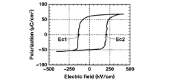
非特許文献1には、結晶構造が正方晶系であるc軸配向PZT膜の特性が評価されている。図13A及び図13Bに、非特許文献1に記載の強誘電体膜の分極−電界特性(FIG.2)と電圧−歪特性(FIG.5)とを示す。この強誘電体膜では、自発分極軸方向と電界印加方向とが一致しており、180°ドメイン反転は起こるが90°ドメイン回転は起こらない。かかる強誘電体の分極−電界特性は角型良好であり、抗電界Ec1,Ec2付近で分極変化がシャープに起こっている。抗電界Ec1,Ec2付近での分極変化は、180°ドメイン反転によるものである。また、かかる系では、電界増加に伴って自発分極軸方向に伸びる電界誘起歪のみが起こるので、電界変化に対して歪は線形に変化する。
Non-Patent
従来一般的な強誘電体では、90°ドメイン回転等の非180°ドメイン回転が起こるので、抗電界Ec1,Ec2付近での分極変化はより緩やかであり、電界−歪特性はヒステリシスを示す。従来一般的な強誘電体では、電界を取り除いても残留分極Prがあり、バイポーラ分極−電界曲線はシングルヒステリシス性を示す。また、バイポーラ分極−電界曲線は原点に対して略対称であり、負電界側の抗電界Ec1の絶対値と正電界側の抗電界Ec2とは略一致する(|Ec1|≒Ec2)。非180°ドメイン回転が起こる従来一般的な強誘電体の分極−電界曲線と電界−歪曲線とを図14に模式的に示す。電界−歪曲線については、バイポーラ駆動とユニポーラ駆動とについて図示してある。 In a conventional general ferroelectric, non-180 ° domain rotation such as 90 ° domain rotation occurs, so that the polarization change near the coercive electric fields Ec1 and Ec2 is more gradual, and the electric field-strain characteristic shows hysteresis. In a conventional general ferroelectric, even if the electric field is removed, there is residual polarization Pr, and the bipolar polarization-electric field curve shows a single hysteresis property. The bipolar polarization-electric field curve is substantially symmetrical with respect to the origin, and the absolute value of the coercive electric field Ec1 on the negative electric field side and the coercive electric field Ec2 on the positive electric field side substantially coincide (| Ec1 | ≈Ec2). FIG. 14 schematically shows a polarization-electric field curve and an electric field-strain curve of a conventional general ferroelectric in which non-180 ° domain rotation occurs. The electric field-strain curve is illustrated for bipolar driving and unipolar driving.
強誘電体は通常、ポーリング処理と称される初期化処理が施された後、使用される。この初期化処理前は強誘電体に種々の自発分極軸方向を持つ多数のドメインが存在するが、初期化処理によって、これら多数のドメインの自発分極軸方向が全体的に揃うようになる。図14のバイポーラ電界−歪曲線及びユニポーラ電界−歪曲線に示すように、この初期化処理では大きな変位が得られる(図中、「1回目」と表記した破線部分を参照)。しかしながら、いったん初期化処理を施すと、電界を取り除いても元の状態に戻らないドメインが多数存在するため、実際の駆動条件となる2回目以降の変位は小さくなる。すなわち、強誘電体では、初期化処理の際には大きな変位が得られるが、その大きな変位は有効利用されていない。 The ferroelectric is usually used after being subjected to an initialization process called a polling process. Before this initialization process, there are many domains having various spontaneous polarization axis directions in the ferroelectric, and the initialization process makes the spontaneous polarization axis directions of these multiple domains uniform as a whole. As shown in the bipolar electric field-strain curve and the unipolar electric field-strain curve in FIG. 14, a large displacement is obtained in this initialization process (see the broken line portion indicated as “first time” in the figure). However, once the initialization process is performed, since there are many domains that do not return to the original state even when the electric field is removed, the second and subsequent displacements, which are the actual driving conditions, are reduced. That is, in the ferroelectric, a large displacement is obtained during the initialization process, but the large displacement is not effectively used.
従来一般的な反強誘電体の分極−電界曲線と電界−歪曲線とを図15に模式的に示す。図15の分極−電界曲線に示すように、反強誘電体は、電界無印加時にはナノスケールで見て1つ1つの格子の分極方向が交互に反転した状態にあるため、全体として分極を示さない(残留分極Pr≒0)。反強誘電体に対して電界を印加すると、すべての格子の分極方向が電界印加方向に揃い、強誘電体のようになる。反強誘電体では、電界を取り除くと元の初期状態に戻るため、バイポーラ分極−電界曲線は原点を通るダブルヒステリシス性を示す。図中、四角に囲まれた矢印は格子の分極方向を模式的に示している。反強誘電体では、強誘電体のように1回目の変位と2回目以降の変位に差は見られない。 FIG. 15 schematically shows a polarization-electric field curve and an electric field-strain curve of a conventional general antiferroelectric material. As shown in the polarization-electric field curve of FIG. 15, the antiferroelectric exhibits polarization as a whole because the polarization direction of each lattice is alternately reversed when viewed on the nanoscale when no electric field is applied. None (residual polarization Pr≈0). When an electric field is applied to the antiferroelectric material, the polarization directions of all the lattices are aligned with the electric field application direction, resulting in a ferroelectric material. In the antiferroelectric material, when the electric field is removed, the original initial state is restored, so that the bipolar polarization-electric field curve exhibits a double hysteresis property passing through the origin. In the figure, arrows surrounded by squares schematically indicate the polarization direction of the lattice. In the antiferroelectric material, unlike the ferroelectric material, there is no difference between the first displacement and the second and subsequent displacements.
従来の反強誘電体では、最大印加電界Emaxと最小印加電界Eminの絶対値とを同一に設定して(Emax=|Emin|)測定されるバイポーラ分極−電界曲線は原点に対して略対称であり、最大分極値Pmaxと最小分極値Pminの絶対値とは略一致する(Pmax≒|Pmin|)。 In the conventional antiferroelectric material, the bipolar polarization-electric field curve measured with the maximum applied electric field Emax and the absolute value of the minimum applied electric field Emin set equal (Emax = | Emin |) is substantially symmetrical with respect to the origin. Yes, the absolute value of the maximum polarization value Pmax and the minimum polarization value Pmin substantially coincide (Pmax≈ | Pmin |).
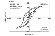
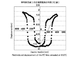
図16A及び図16Bに反強誘電体の実際の分極−電界曲線と電界−歪曲線の測定データ例を示す。これらの測定データは、非特許文献2のFig.2及びFig.8に記載されたPbZrO3(PZ)膜のデータである。圧電定数に関するデータの記載はないが、本発明者が電界−歪曲線のグラフ中に示す破線の傾きから圧電定数を求めたところ、0〜400kV/cmで駆動したときの圧電定数d33=150pm/V程度、d31=75pm/V程度であった。反強誘電体−強誘電体間の相転移から大きな変位が期待されたが、PZT系を凌駕する圧電性能は得られていない。 FIG. 16A and FIG. 16B show measurement data examples of actual polarization-electric field curves and electric field-strain curves of antiferroelectric materials. These measurement data are shown in FIG. 2 and FIG. 8 is a data of the PbZrO 3 (PZ) film described in FIG. Although there is no description of data relating to the piezoelectric constant, when the present inventor obtained the piezoelectric constant from the slope of the broken line shown in the graph of the electric field-strain curve, the piezoelectric constant d 33 = 150 pm when driven at 0 to 400 kV / cm. / V about, was about d 31 = 75pm / V. Although a large displacement was expected from the phase transition between the antiferroelectric material and the ferroelectric material, piezoelectric performance surpassing that of the PZT system has not been obtained.
図15のバイポーラ電界−歪曲線に示すように、反強誘電体の変位はある電界強度で変位が急激に増加するデジタル的な変位である。かかるデジタル的な変位は、圧電アクチュエータ等の用途には適していない。また、反強誘電体は周波数特性が良くなく、50Hz程度までは良好な変位が得られるが、それ以上の周波数をかけると変位が落ちてしまう。圧電アクチュエータでは通常100Hz以上の周波数をかけるため、反強誘電体は圧電アクチュエータ等の用途には適していない。 As shown in the bipolar electric field-strain curve of FIG. 15, the displacement of the antiferroelectric material is a digital displacement in which the displacement rapidly increases at a certain electric field strength. Such digital displacement is not suitable for applications such as piezoelectric actuators. Further, the antiferroelectric material has poor frequency characteristics, and a good displacement can be obtained up to about 50 Hz. However, if a frequency higher than that is applied, the displacement drops. Since a piezoelectric actuator usually applies a frequency of 100 Hz or more, the antiferroelectric material is not suitable for applications such as a piezoelectric actuator.
近年、強誘電体において、バイポーラ分極−電界曲線が対称ダブルヒステリシスを示す材料が報告されている。 In recent years, in ferroelectrics, materials have been reported in which the bipolar polarization-electric field curve exhibits symmetrical double hysteresis.
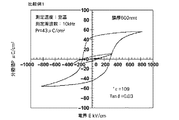
非特許文献3には、アクセプタイオンであるMnとドナイオンであるNbを共ドープしたランダム配向のBaTiO3バルクセラミックスを製造した後、60℃で64hrのエージング処理を施した材料が、対称ダブルヒステリシス分極−電界特性を示すことが報告されている。図17A及び図17Bに非特許文献3に記載の材料の分極−電界曲線と電界−歪曲線の測定データを示す(非特許文献3のFig.1及びFig.3)。圧電定数に関するデータの記載はないが、本発明者が電界−歪曲線のグラフ中に示す破線の傾きから圧電定数を求めたところ、最も大きいもので、0〜3kV/cmで駆動したときの圧電定数d33=550pm/V程度、d31=225pm/V程度であった(図17B(非特許文献3のFig.3)(a)を参照)。この材料は非鉛系にも関わらず、大きな変位が得られている。
非特許文献4には、MnをドープしたBaTiO3単結晶を製造した後、80℃で2週間のエージング処理を施した材料が、対称ダブルヒステリシス分極−電界特性を示すことが報告されている。
非特許文献3,4には、上記材料が90°ドメイン回転を示すことが記載されており、材料特性のメカニズムが以下のように記載されている(非特許文献3Fig.4等を参照)。
Mn及びNb、あるいはMn単独をドープすることによって、強誘電ドメイン内に移動性の点欠陥が生じる。エージング処理を施すと、移動性の点欠陥が安定な位置に移動して酸素欠陥とペアを作り、その短距離秩序の対称性が強誘電ドメインの結晶対称性に一致するようになる。これによって、強誘電ドメイン内に、その自発分極方向と一致した方向に分極した欠陥分極(defect dipole)が生じる。電界を印加すると、強誘電ドメインの90°ドメイン回転が起こるが、上記欠陥分極の分極方向は変化しない。強誘電ドメインの分極方向と欠陥分極の分極方向が一致した状態が安定であるため、電界を取り除くと、強誘電ドメインは元の安定な分極方向の状態に戻る。欠陥分極の存在によって強誘電ドメインが初期状態に戻ることで、電界を繰り返し増減させても大きな変位が得られ、対称ダブルヒステリシス分極−電界特性を示す。
Doping with Mn and Nb, or Mn alone, creates mobile point defects in the ferroelectric domain. When the aging treatment is performed, the mobile point defect moves to a stable position to form a pair with the oxygen defect, and the short-range order symmetry coincides with the crystal symmetry of the ferroelectric domain. As a result, a defect dipole polarized in a direction corresponding to the spontaneous polarization direction is generated in the ferroelectric domain. When an electric field is applied, 90 ° domain rotation of the ferroelectric domain occurs, but the polarization direction of the defect polarization does not change. Since the state in which the polarization direction of the ferroelectric domain coincides with the polarization direction of the defect polarization is stable, the ferroelectric domain returns to the original stable polarization direction when the electric field is removed. Since the ferroelectric domain returns to the initial state due to the presence of defect polarization, a large displacement can be obtained even when the electric field is repeatedly increased or decreased, and a symmetrical double hysteresis polarization-electric field characteristic is exhibited.
圧電アクチュエータ等の用途では、強誘電体は通常ユニポーラ駆動で使用される。ダブルヒステリシス分極−電界特性を示す材料は、電界無印加時に初期状態に戻り、残留分極Prが0若しくはそれに近い値となるため、残留分極Prの大きいシングルヒステリシス分極−電界特性を示す材料よりも大きな変位が期待される。
電子機器の小型軽量化・高機能化に伴い、これに搭載される圧電素子においても小型軽量化・高機能化が進められるようになってきている。例えば、インクジェット式記録ヘッドでは、高画質化のために、圧電素子の高密度化が検討されており、それに伴って強誘電体の薄膜化が検討されている。 As electronic devices become smaller, lighter and more functional, piezoelectric elements mounted on the electronic devices are becoming smaller, lighter and more functional. For example, in an ink jet recording head, increasing the density of piezoelectric elements is being studied in order to improve image quality, and accordingly, making a ferroelectric thin film is being studied.
非特許文献3,4では、バルクセラミックスあるいはバルク単結晶について研究がなされているにすぎず、膜については一切言及されていない。すなわち、従来は、ダブルヒステリシス分極−電界特性を示す強誘電体膜及びその製造方法に関する研究例は一切報告されていない。また、非特許文献3,4に記載の強誘電体の製造方法は、長時間のエージング処理が必要であり、製造効率も良くない。
In
本発明は上記事情に鑑みてなされたものであり、バイポーラ分極−電界曲線がダブルヒステリシス性を示し、大きな変位が期待される強誘電体膜、及びこの強誘電体膜を用いた圧電素子及び液体吐出装置を提供することを目的とするものである。 The present invention has been made in view of the above circumstances, and a ferroelectric film in which a bipolar polarization-electric field curve exhibits double hysteresis properties and a large displacement is expected, and a piezoelectric element and a liquid using the ferroelectric film The object is to provide a discharge device.
本発明の強誘電体膜は、最大印加電界Emaxと最小印加電界Eminの絶対値とを同一に設定して(Emax=|Emin|)測定されるバイポーラ分極−電界曲線が、少なくとも5個の変曲点を有し、かつ、最大分極値Pmaxと最小分極値Pminの絶対値とが略等しい(Pmax≒|Pmin|)ダブルヒステリシス性を有することを特徴とするものである。 In the ferroelectric film of the present invention, the bipolar polarization-electric field curve measured by setting the maximum applied electric field Emax and the absolute value of the minimum applied electric field Emin to be the same (Emax = | Emin |) has at least five variations. It has a bend point, and has a double hysteresis property (Pmax≈ | Pmin |) in which the absolute value of the maximum polarization value Pmax and the minimum polarization value Pmin are substantially equal.
バイポーラ分極−電界曲線が原点を通るダブルヒステリシス性を示すとき変曲点数は基本的に5個であり、原点を通らないダブルヒステリシス性を示すとき変曲点数は基本的に6個である。 The number of inflection points is basically 5 when the bipolar polarization-electric field curve shows double hysteresis passing through the origin, and the number of inflection points is basically 6 when showing double hysteresis not passing through the origin.
本明細書において、「バイポーラ分極−電界曲線が少なくとも5個の変曲点を有する」とは、バイポーラ分極−電界特性の実測データを基にバイポーラ分極−電界曲線を描き、EminからEmaxに電界を増加させたときの片道の曲線とEmaxからEminに電界を減少させたときの片道の曲線とに分けてそれぞれ通常のカーブフィッティング処理及びスムージング処理を施したものについて、少なくとも5個の変曲点を有することを意味する。「変曲点」には、測定ノイズによる微小データ変動に基づく変曲点は含まれないものとする。測定ノイズが多い場合には、アベレージング処理や繰返し積算処理等によって測定ノイズを取り除いた後、カーブフィッティング処理を施すものとする。 In this specification, “the bipolar polarization-electric field curve has at least five inflection points” means that the bipolar polarization-electric field curve is drawn based on the measured data of the bipolar polarization-electric field characteristics, and the electric field is applied from Emin to Emax. At least 5 inflection points are obtained for the one-way curve when increased and the one-way curve when the electric field is decreased from Emax to Emin and subjected to normal curve fitting processing and smoothing processing, respectively. It means having. The “inflection point” does not include an inflection point based on a minute data variation due to measurement noise. When the measurement noise is large, the curve fitting process is performed after the measurement noise is removed by averaging process, repeated integration process, or the like.
図14に示した通常のシングルヒステリシス分極−電界曲線の変曲点は2個であるので、バイポーラ分極−電界曲線が少なくとも5個の変曲点を有するということは、バイポーラ分極−電界特性がダブルヒステリシス性を有することを意味する。 Since there are two inflection points of the normal single hysteresis polarization-electric field curve shown in FIG. 14, the bipolar polarization-electric field curve has at least five inflection points. It means having hysteresis.
本明細書において、「Pmax≒|Pmin|」とは、Pmaxと|Pmin|との差が、Pmaxと|Pmin|とのうち値が大きい方の10%以下であることと定義する。 In this specification, “Pmax≈ | Pmin |” is defined as the difference between Pmax and | Pmin | being 10% or less of the larger value of Pmax and | Pmin |.
本発明の強誘電体膜のバイポーラ分極−電界曲線は、原点に対して略対称な対称ダブルヒステリシス性を有していてもよいし、原点に対して非対称な非対称ダブルヒステリシス性を有していてもよい。 The bipolar polarization-electric field curve of the ferroelectric film of the present invention may have a symmetric double hysteresis property that is substantially symmetrical with respect to the origin, or an asymmetric double hysteresis property that is asymmetric with respect to the origin. Also good.
本発明の強誘電体膜は、1種又は2種以上のペロブスカイト型酸化物からなる(不可避不純物を含んでいてもよい)ことが好ましく、下記一般式(P)で表される1種又は2種以上のペロブスカイト型酸化物からなる(不可避不純物を含んでいてもよい)ことがより好ましい。
一般式ABO3・・・(P)
(式中、A:Aサイトの元素であり、Pb,Ba,Sr,Bi,Li,Na,Ca,Cd,Mg,K,及びランタニド元素からなる群より選ばれた少なくとも1種の元素、
B:Bサイトの元素であり、Ti,Zr,V,Nb,Ta,Cr,Mo,W,Mn,Mg,Sc,Co,Cu,In,Sn,Ga,Zn,Cd,Fe,Ni,Hf,及びAlからなる群より選ばれた少なくとも1種の元素、
O:酸素元素、
Aサイト元素とBサイト元素と酸素元素のモル比は1:1:3が標準であるが、これらのモル比はペロブスカイト構造を取り得る範囲内で基準モル比からずれてもよい。)
The ferroelectric film of the present invention is preferably composed of one or more perovskite oxides (may contain inevitable impurities), and is represented by one or two represented by the following general formula (P) More preferably, it is made of a perovskite type oxide of at least one species (may contain inevitable impurities).
General formula ABO 3 (P)
(In the formula, A: an element of A site, Pb, Ba, Sr, Bi, Li, Na, Ca, Cd, Mg, K, and at least one element selected from the group consisting of lanthanide elements,
B: Element of B site, Ti, Zr, V, Nb, Ta, Cr, Mo, W, Mn, Mg, Sc, Co, Cu, In, Sn, Ga, Zn, Cd, Fe, Ni, Hf , And at least one element selected from the group consisting of Al,
O: oxygen element,
The molar ratio of the A site element, the B site element, and the oxygen element is 1: 1: 3 as a standard, but these molar ratios may deviate from the reference molar ratio within a range where a perovskite structure can be taken. )
本発明の強誘電体膜は、前記一般式(P)で表され、かつ、Aサイトが、Pb,Bi,Ba,Sr,Ca,La,及びMgからなる群より選ばれた少なくとも1種の金属元素からなり、Bサイトが、Zr,Ti,Fe,及びAlからなる群より選ばれた少なくとも1種の金属元素と、Co,Mn,Mg,Ni,Zn,V,Nb,Ta,Cr,Mo,及びWからなる群より選ばれた少なくとも1種の金属元素とからなるペロブスカイト型酸化物(P1)を含むことが好ましい。 The ferroelectric film of the present invention is represented by the general formula (P), and the A site is at least one selected from the group consisting of Pb, Bi, Ba, Sr, Ca, La, and Mg. It is made of a metal element, and the B site is at least one metal element selected from the group consisting of Zr, Ti, Fe, and Al, and Co, Mn, Mg, Ni, Zn, V, Nb, Ta, Cr, It is preferable to include a perovskite oxide (P1) composed of at least one metal element selected from the group consisting of Mo and W.
本発明の強誘電体膜は、前記一般式(P)で表され、かつ、AサイトがBiを主成分とし、BサイトがFeを主成分とするペロブスカイト型酸化物(P2)を含む構成も好ましい。
本明細書において、「Aサイト(あるいはBサイト)の主成分」はAサイト(あるいはBサイト)中80モル%以上の成分と定義する。
The ferroelectric film of the present invention is also represented by the general formula (P), and the A site includes a perovskite oxide (P2) whose main component is Bi and whose B site is mainly Fe. preferable.
In this specification, “the main component of the A site (or B site)” is defined as a component of 80 mol% or more in the A site (or B site).
本発明の強誘電体膜は、前記一般式(P)で表され、かつ、AサイトがBi及び少なくとも1種のランタニド元素を含み、BサイトがFe及びAlを含むペロブスカイト型酸化物(P3)を含む構成も好ましい。
本発明の強誘電体膜は、一般式xBiFeO3−(1−x)BaTiO3(式中、0<x<1.0)で表されるペロブスカイト型酸化物(P4)を含む構成も好ましい。
The ferroelectric film of the present invention is a perovskite oxide (P3) represented by the general formula (P), wherein the A site contains Bi and at least one lanthanide element, and the B site contains Fe and Al. The structure containing is also preferable.
The ferroelectric film of the present invention preferably includes a perovskite oxide (P4) represented by the general formula xBiFeO 3- (1-x) BaTiO 3 (where 0 <x <1.0).
本発明の強誘電体膜は、結晶配向性を有する強誘電体相を含むことが好ましい。
本明細書において、「結晶配向性を有する」とは、Lotgerling法により測定される配向率Fが、80%以上であることと定義する。
配向率Fは、下記式(i)で表される。
F(%)=(P−P0)/(1−P0)×100・・・(i)
式(i)中、Pは、配向面からの反射強度の合計と全反射強度の合計の比である。(001)配向の場合、Pは、(00l)面からの反射強度I(00l)の合計ΣI(00l)と、各結晶面(hkl)からの反射強度I(hkl)の合計ΣI(hkl)との比({ΣI(00l)/ΣI(hkl)})である。例えば、ペロブスカイト結晶において(001)配向の場合、P=I(001)/[I(001)+I(100)+I(101)+I(110)+I(111)]である。
P0は、完全にランダムな配向をしている試料のPである。
完全にランダムな配向をしている場合(P=P0)にはF=0%であり、完全に配向をしている場合(P=1)にはF=100%である。
The ferroelectric film of the present invention preferably contains a ferroelectric phase having crystal orientation.
In this specification, “having crystal orientation” is defined as an orientation rate F measured by the Lottgering method being 80% or more.
The orientation rate F is represented by the following formula (i).
F (%) = (P−P0) / (1−P0) × 100 (i)
In formula (i), P is the ratio of the total reflection intensity from the orientation plane to the total reflection intensity. In the case of (001) orientation, P is the sum ΣI (00l) of the reflection intensity I (00l) from the (00l) plane and the sum ΣI (hkl) of the reflection intensity I (hkl) from each crystal plane (hkl). ({ΣI (00l) / ΣI (hkl)}). For example, in the case of (001) orientation in the perovskite crystal, P = I (001) / [I (001) + I (100) + I (101) + I (110) + I (111)].
P0 is P of a sample having a completely random orientation.
When the orientation is completely random (P = P0), F = 0%, and when the orientation is complete (P = 1), F = 100%.
本発明の強誘電体膜は、(100)配向の強誘電体相及び/又は(111)配向の強誘電体相を含むことができる。
本発明の強誘電体膜は、(100)配向の正方晶相及び/又は(111)配向の菱面体晶相を含むことができる。
The ferroelectric film of the present invention can include a (100) -oriented ferroelectric phase and / or a (111) -oriented ferroelectric phase.
The ferroelectric film of the present invention can include a (100) oriented tetragonal phase and / or a (111) oriented rhombohedral phase.
本発明の強誘電体膜は、モルフォトロピック相境界(MPB)又はその近傍の組成を有し、正方晶相、斜方晶相、及び菱面体晶相からなる群より選択される少なくとも2つの結晶相を含む構成を有することができる。
「MPB又はその近傍」とは、電界をかけた時に相転移する領域のことである。
The ferroelectric film of the present invention has a composition at or near the morphotropic phase boundary (MPB) and has at least two crystals selected from the group consisting of a tetragonal phase, an orthorhombic phase, and a rhombohedral phase. It can have a configuration that includes phases.
“MPB or its vicinity” refers to a region that undergoes a phase transition when an electric field is applied.
本発明の強誘電体膜は、自発分極軸方向とは異なる方向に結晶配向性を有する強誘電体相を含むことが好ましい。
自発分極軸方向とは異なる方向に結晶配向性を有する前記強誘電体相は、略<100>方向に結晶配向性を有する菱面体晶相、略<110>方向に結晶配向性を有する菱面体晶相、略<110>方向に結晶配向性を有する正方晶相、略<111>方向に結晶配向性を有する正方晶相、略<100>方向に結晶配向性を有する斜方晶相、及び略<111>方向に結晶配向性を有する斜方晶相からなる群より選択された少なくとも1つの強誘電体相であることが好ましい。
本明細書において、「略<abc>方向に結晶配向性を有する」とは、その方向の結晶配向率Fが80%以上であると定義する。
The ferroelectric film of the present invention preferably includes a ferroelectric phase having crystal orientation in a direction different from the spontaneous polarization axis direction.
The ferroelectric phase having crystal orientation in a direction different from the spontaneous polarization axis direction is a rhombohedral phase having crystal orientation in a substantially <100> direction, and a rhombohedral having crystal orientation in a substantially <110> direction. A crystal phase, a tetragonal phase having crystal orientation in a substantially <110> direction, a tetragonal phase having crystal orientation in a substantially <111> direction, an orthorhombic phase having crystal orientation in a substantially <100> direction, and It is preferable that the phase is at least one ferroelectric phase selected from the group consisting of orthorhombic phases having crystal orientation in a substantially <111> direction.
In this specification, “having crystal orientation in the substantially <abc> direction” is defined as the crystal orientation ratio F in that direction being 80% or more.
自発分極軸方向とは異なる方向に結晶配向性を有する前記強誘電体相は、該強誘電体相の自発分極軸方向とは異なる方向の電界印加により、該強誘電体相の少なくとも一部が相転移する性質を有するものであることが好ましい。 The ferroelectric phase having crystal orientation in a direction different from the spontaneous polarization axis direction is such that at least part of the ferroelectric phase is applied by applying an electric field in a direction different from the spontaneous polarization axis direction of the ferroelectric phase. It is preferable that the material has a phase transition property.
本発明の圧電素子は、上記の本発明の強誘電体膜からなる圧電体と、該圧電体に対して電界を印加する電極とを備えたことを特徴とするものである。
本発明の液体吐出装置は、上記の本発明の圧電素子と、
液体が貯留される液体貯留室及び該液体貯留室から外部に前記液体が吐出される液体吐出口を有する液体貯留吐出部材とを備えたことを特徴とするものである。
The piezoelectric element of the present invention is characterized by comprising a piezoelectric body made of the ferroelectric film of the present invention and an electrode for applying an electric field to the piezoelectric body.
The liquid ejection device of the present invention includes the above-described piezoelectric element of the present invention,
A liquid storage chamber in which liquid is stored, and a liquid storage and discharge member having a liquid discharge port through which the liquid is discharged from the liquid storage chamber are provided.
本発明は、最大印加電界Emaxと最小印加電界Eminの絶対値とを同一に設定して(Emax=|Emin|)測定されるバイポーラ分極−電界曲線が、少なくとも5個の変曲点を有し、かつ、最大分極値Pmaxと最小分極値Pminの絶対値とが略等しい(Pmax≒|Pmin|)ダブルヒステリシス性を有する強誘電体膜をはじめて実現したものである。 In the present invention, the bipolar polarization-electric field curve measured by setting the maximum applied electric field Emax and the absolute value of the minimum applied electric field Emin to be equal (Emax = | Emin |) has at least five inflection points. In addition, this is the first realization of a ferroelectric film having a double hysteresis property in which the absolute value of the maximum polarization value Pmax and the minimum polarization value Pmin are substantially equal (Pmax≈ | Pmin |).
上記ダブルヒステリシス分極−電界特性を示す強誘電体膜は、電界無印加時に初期状態に戻るため、残留分極Prの大きいシングルヒステリシス分極−電界特性を示す通常の強誘電体膜よりも残留分極Prがより小さくなる傾向にあり、より大きな変位が期待される。 Since the ferroelectric film showing the double hysteresis polarization-electric field characteristics returns to the initial state when no electric field is applied, the residual polarization Pr is higher than that of a normal ferroelectric film showing a single hysteresis polarization-electric field characteristics having a large residual polarization Pr. There is a tendency to become smaller, and a larger displacement is expected.
「強誘電体膜」
<分極−電界特性>
本発明の強誘電体膜は、最大印加電界Emaxと最小印加電界Eminの絶対値とを同一に設定して(Emax=|Emin|)測定されるバイポーラ分極−電界曲線が、少なくとも5個の変曲点を有し、かつ、最大分極値Pmaxと最小分極値Pminの絶対値とが略等しい(Pmax≒|Pmin|)ダブルヒステリシス性を有する膜である。
"Ferroelectric film"
<Polarization-electric field characteristics>
In the ferroelectric film of the present invention, the bipolar polarization-electric field curve measured by setting the maximum applied electric field Emax and the absolute value of the minimum applied electric field Emin to be the same (Emax = | Emin |) has at least five variations. The film has a bending point and has a double hysteresis property (Pmax≈ | Pmin |) in which the absolute value of the maximum polarization value Pmax and the minimum polarization value Pmin are substantially equal.
図14に示した通常のシングルヒステリシス分極−電界曲線の変曲点は2個であるので、バイポーラ分極−電界曲線が少なくとも5個の変曲点を有するということは、バイポーラ分極−電界特性がダブルヒステリシス性を有することを意味する。 Since there are two inflection points of the normal single hysteresis polarization-electric field curve shown in FIG. 14, the bipolar polarization-electric field curve has at least five inflection points. It means having hysteresis.
本発明の強誘電体膜において、バイポーラ分極−電界曲線は原点を通るダブルヒステリシス性を示すものでも、原点を通らないダブルヒステリシス性を示すものでもよい。バイポーラ分極−電界曲線が原点を通るダブルヒステリシス性を示すとき変曲点数は基本的に5個であり、原点を通らないダブルヒステリシス性を示すとき変曲点数は基本的に6個である。 In the ferroelectric film of the present invention, the bipolar polarization-electric field curve may exhibit a double hysteresis property that passes through the origin, or may exhibit a double hysteresis property that does not pass through the origin. The number of inflection points is basically 5 when the bipolar polarization-electric field curve shows double hysteresis passing through the origin, and the number of inflection points is basically 6 when showing double hysteresis not passing through the origin.
本発明の強誘電体膜のバイポーラ分極−電界曲線は、原点に対して略対称な対称ダブルヒステリシス性を有していてもよいし、原点に対して非対称な非対称ダブルヒステリシス性を有していてもよい。 The bipolar polarization-electric field curve of the ferroelectric film of the present invention may have a symmetric double hysteresis property that is substantially symmetrical with respect to the origin, or an asymmetric double hysteresis property that is asymmetric with respect to the origin. Also good.
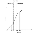
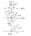
図1に、本発明の強誘電体膜のバイポーラ分極−電界ヒステリシス曲線(P−Eヒステリシス曲線)、バイポーラ電界−歪曲線、及びユニポーラ電界−歪曲線の例を模式的に示す。ここでは、バイポーラ分極−電界ヒステリシス曲線が原点を通り、原点に対して略対称なダブルヒステリシス性を示す場合について示してある。 FIG. 1 schematically shows examples of a bipolar polarization-electric field hysteresis curve (PE hysteresis curve), a bipolar electric field-strain curve, and a unipolar electric field-strain curve of the ferroelectric film of the present invention. Here, a case is shown in which the bipolar polarization-electric field hysteresis curve passes through the origin and exhibits a double hysteresis property that is substantially symmetrical with respect to the origin.
図2に、図1の分極−電界ヒステリシス曲線とその変曲点を示しておく。図示するバイポーラ分極−電界曲線は原点を通っているので、原点に最も近い変曲点の分極値をPif0としたとき、Pif0=0である。 FIG. 2 shows the polarization-electric field hysteresis curve of FIG. 1 and its inflection point. Since the illustrated bipolar polarization-electric field curve passes through the origin, when the inflection point closest to the origin is Pif 0 , Pif 0 = 0.
強誘電体でありながらダブルヒステリシス分極−電界特性を示す材料は過去にほとんど報告がなく、「背景技術」の項で挙げた非特許文献3,4にのみ報告されている。しかも、非特許文献3,4に記載の強誘電体はBaTiO3系のバルクセラミックスあるいはバルク単結晶のみである。
Although there are few reports in the past regarding materials exhibiting double hysteresis polarization-electric field characteristics even though they are ferroelectrics, they are only reported in
インクジェット式記録ヘッド等の用途では、高画質化等のために、圧電素子の高密度化が検討されており、それに伴って圧電素子の薄型化が検討されている。圧電素子の薄型化を考慮すれば、強誘電体としては強誘電体膜が好ましく、厚み20μm以下の強誘電体薄膜がより好ましい。 In applications such as an ink jet recording head, increasing the density of piezoelectric elements has been studied in order to improve image quality, and accordingly, reducing the thickness of piezoelectric elements has been studied. Considering thinning of the piezoelectric element, a ferroelectric film is preferable as the ferroelectric, and a ferroelectric thin film having a thickness of 20 μm or less is more preferable.
本発明者は、最大印加電界Emaxと最小印加電界Eminの絶対値とを同一に設定して(Emax=|Emin|)測定されるバイポーラ分極−電界曲線が、少なくとも5個の変曲点を有し、かつ、最大分極値Pmaxと最小分極値Pminの絶対値とが略等しい(Pmax≒|Pmin|)ダブルヒステリシス分極−電界特性を示すPZT系強誘電体膜をはじめて実現した。非特許文献3,4に記載の強誘電体の製造方法では長時間のエージング処理が必要であるが、本発明者はかかるエージング処理を要することなく、ダブルヒステリシス分極−電界特性を示すPZT系強誘電体膜を成膜することを実現した。
The inventor of the present invention has at least five inflection points in the bipolar polarization-electric field curve measured by setting the absolute value of the maximum applied electric field Emax and the absolute value of the minimum applied electric field Emin to be the same (Emax = | Emin |). In addition, a PZT ferroelectric film exhibiting double hysteresis polarization-electric field characteristics was realized for the first time, with the absolute value of the maximum polarization value Pmax and the minimum polarization value Pmin being substantially equal (Pmax≈ | Pmin |). Although the ferroelectric manufacturing methods described in
圧電アクチュエータ等の用途では、強誘電体は通常ユニポーラ駆動で使用される。ダブルヒステリシス分極−電界特性を示す材料は、電界無印加時に初期状態に戻るため、残留分極Prの大きいシングルヒステリシス分極−電界特性を示す通常の強誘電体膜よりも残留分極Prがより小さくなる傾向にあり、より大きな変位が期待される。ダブルヒステリシス分極−電界特性を示す材料では、残留分極Prを0若しくはそれに近い値とすることもでき、より大きな変位が期待される。 In applications such as piezoelectric actuators, ferroelectrics are usually used with unipolar drive. Since a material exhibiting double hysteresis polarization-electric field characteristics returns to an initial state when no electric field is applied, the residual polarization Pr tends to be smaller than that of a normal ferroelectric film exhibiting single hysteresis polarization-electric field characteristics having a large residual polarization Pr. Therefore, a larger displacement is expected. In a material exhibiting double hysteresis polarization-electric field characteristics, the residual polarization Pr can be set to 0 or a value close thereto, and a larger displacement is expected.
図1に示すように、対称ダブルヒステリシス分極−電界特性を示す本発明の強誘電体膜は、バイポーラ電界−歪曲線はy軸(歪量を示す軸)に対して略対称であり、正電界側のユニポーラ電界−歪曲線と負電界側のユニポーラ電界−歪曲線とは略同一の傾向を示す。図1では、正電界側を例として、ユニポーラ電界−歪曲線を図示してある。 As shown in FIG. 1, the ferroelectric film of the present invention showing symmetric double hysteresis polarization-electric field characteristics has a bipolar electric field-strain curve that is substantially symmetric with respect to the y-axis (axis indicating the amount of strain). The unipolar electric field-strain curve on the side and the unipolar electric field-strain curve on the negative field side show substantially the same tendency. In FIG. 1, a unipolar electric field-strain curve is illustrated by taking the positive electric field side as an example.
非対称ダブルヒステリシス分極−電界特性を示す本発明の強誘電体膜においても、最大分極値Pmaxと最小分極値Pminの絶対値とが略等しい(Pmax≒|Pmin|)ダブルヒステリシス性を有するので、正電界側で駆動しても負電界側で駆動しても、同等レベルの圧電歪が得られる。 Also in the ferroelectric film of the present invention showing the asymmetric double hysteresis polarization-electric field characteristics, the absolute value of the maximum polarization value Pmax and the minimum polarization value Pmin is substantially equal (Pmax≈ | Pmin |). An equivalent level of piezoelectric strain can be obtained whether driven on the electric field side or on the negative electric field side.
本発明の強誘電体膜において、バイポーラ分極−電界曲線は原点を通ってもよいし、原点を通らなくてもよいことを述べたが、原点に最も近い変曲点の分極値をPif0としたとき、Pif0≒0であることが好ましい。図1に示したように、Pif0=0のときバイポーラ分極−電界曲線は完全に原点を通る曲線となり、残留分極Pr=0となる。Pif0≒0であれば、バイポーラ分極−電界曲線はほぼ原点を通る曲線となるので、残留分極Pr≒0となり、大きな変位が期待される。
In the ferroelectric film of the present invention, it has been described that the bipolar polarization-electric field curve may or may not pass through the origin, but the polarization value at the inflection point closest to the origin is Pif 0 . Then, it is preferable that Pif 0 ≈0. As shown in FIG. 1, the bipolar polarization when
従来、反強誘電体では、対称ダブルヒステリシス分極−電界特性を示す膜が報告されているが、強誘電体では、ダブルヒステリシス分極−電界特性を示す膜は一切報告されていない。「背景技術」の項において説明したように、ある電界強度で変位が急激に増加するデジタル的な変位を示し、周波数特性が良くない反強誘電体は、圧電アクチュエータ等の用途には適していない。ダブルヒステリシス分極−電界特性を示す強誘電体膜を実現できたことは、技術的価値が大きい。 Conventionally, a film exhibiting symmetric double hysteresis polarization-electric field characteristics has been reported for antiferroelectrics, but no film exhibiting double hysteresis polarization-electric field characteristics has been reported for ferroelectrics. As described in the “Background Art” section, an antiferroelectric material that exhibits a digital displacement in which the displacement rapidly increases at a certain electric field strength and has poor frequency characteristics is not suitable for applications such as a piezoelectric actuator. . The realization of a ferroelectric film exhibiting double hysteresis polarization-electric field characteristics is of great technical value.
本発明の強誘電体膜がダブルヒステリシス分極−電界特性を示すメカニズムは必ずしも明らかではないが、本発明者は以下のように推察している。
「背景技術」の項において、反強誘電体は、電界無印加時にはナノスケールで見て1つ1つの結晶格子の分極方向が交互に反転した状態にあるため、全体として残留分極を示さない(残留分極Pr≒0)ことを述べた。図1に示す分極−電界特性を有する本発明の強誘電体は、電界無印加時において反強誘電体ライクの状態にあると推察される。
The mechanism by which the ferroelectric film of the present invention exhibits double hysteresis polarization-electric field characteristics is not necessarily clear, but the present inventors infer as follows.
In the “Background Art” section, the antiferroelectric material shows no remanent polarization as a whole because the polarization direction of each crystal lattice is alternately reversed when viewed on the nanoscale when no electric field is applied ( It has been described that the remanent polarization Pr≈0). The ferroelectric of the present invention having the polarization-electric field characteristics shown in FIG. 1 is presumed to be in an antiferroelectric-like state when no electric field is applied.
格子・ドメインなどのミクロな状態の詳細は明らかではないが、本発明者は以下の仮説を考えている。 Although details of the microscopic state such as the lattice / domain are not clear, the present inventor considers the following hypothesis.
図3に模式的に示すように、図1に示す分極−電界特性を有する本発明の強誘電体は、電界無印加時には結晶格子よりも大きなマクロスケールで見て隣り合うドメインの分極方向が互いの分極を相殺する方向で安定化しており、全体として残留分極を示さない(残留分極Pr≒0)のではないかと推測される。この強誘電体に対して電界を印加すると、全体的にドメインの分極方向が電界印加方向に揃って、分極が生じると推察される。この強誘電体では、電界を取り除くと元の安定な反強誘電体ライクな初期状態に戻り、バイポーラ分極−電界曲線は原点を通るダブルヒステリシス性を示すと推察される。 As schematically shown in FIG. 3, the ferroelectric of the present invention having the polarization-electric field characteristics shown in FIG. 1 has the polarization directions of adjacent domains viewed from each other on a macro scale larger than the crystal lattice when no electric field is applied. It is presumed that the residual polarization is not shown as a whole (residual polarization Pr≈0). When an electric field is applied to this ferroelectric substance, it is presumed that the polarization direction of the domain is entirely aligned with the electric field application direction and polarization occurs. In this ferroelectric, when the electric field is removed, it returns to the original stable antiferroelectric-like initial state, and it is presumed that the bipolar polarization-electric field curve exhibits a double hysteresis property passing through the origin.
本発明の強誘電体の分極−電界曲線は原点を通らない場合もあるが、この場合も図14に示した通常のシングルヒステリシス分極−電界特性の強誘電体に比較して残留分極Prは小さく、図1に示す分極−電界特性を有する強誘電体と図14に示した通常のシングルヒステリシス分極−電界特性の強誘電体との中間的な状態にあると考えられる。 The polarization-electric field curve of the ferroelectric of the present invention may not pass through the origin, but in this case as well, the residual polarization Pr is smaller than that of the normal single hysteresis polarization-electric field characteristic ferroelectric shown in FIG. 1 is considered to be in an intermediate state between the ferroelectric having polarization-electric field characteristics shown in FIG. 1 and the normal single hysteresis polarization-electric field ferroelectric shown in FIG.
図3では例として、1つ1つのドメインの分極方向が交互に180°反転している場合について図示してある。通常、強誘電体は、下部電極と強誘電体と上部電極とが順次積み重ねられた強誘電体素子(圧電素子)の形態で使用され、下部電極と上部電極とのうち、一方の電極を印加電圧が0Vに固定されるグランド電極とし、他方の電極を印加電圧が変動されるアドレス電極として、駆動される。通常は、下部電極をグランド電極とし、上部電極をアドレス電極として駆動するので、図3において、分極が上向きのドメイン(分極の+側が上部電極側であり、分極の−側が下部電極側であるドメイン)を↑ドメイン、分極が下向きのドメイン(分極の+側が下部電極側であり、分極の−側が上部電極側であるドメイン)を↓ドメインと表記してある。分極の上向き・下向きは、便宜上のものである。 In FIG. 3, as an example, the case where the polarization directions of each domain are alternately inverted by 180 ° is illustrated. Usually, a ferroelectric is used in the form of a ferroelectric element (piezoelectric element) in which a lower electrode, a ferroelectric, and an upper electrode are sequentially stacked, and one of the lower electrode and the upper electrode is applied. The ground electrode whose voltage is fixed at 0V is used, and the other electrode is driven as an address electrode whose applied voltage is varied. Normally, the lower electrode is driven as a ground electrode and the upper electrode is driven as an address electrode. Therefore, in FIG. 3, the domain whose polarization is upward (the domain where the polarization + side is the upper electrode side and the polarization -side is the lower electrode side) ) Is a domain, and a domain whose polarization is downward (a domain in which the + side of polarization is the lower electrode side and the − side of polarization is the upper electrode side) is expressed as the ↓ domain. The upward and downward polarization is for convenience.
図3の分極−電界曲線のグラフにおいては、分極が完全上向きのドメインと分極が完全下向きのドメインのみを図示してあるが、電界無印加時のドメインの分極方向は、電界印加方向に対して斜め方向あるいは垂直方向の場合もある。また、電界無印加時のドメインの分極方向は横向き方向あるいはそれに近い斜め方向の場合もある。 In the polarization-electric field curve graph of FIG. 3, only the domain in which the polarization is completely upward and the domain in which the polarization is completely downward are illustrated, but the polarization direction of the domain when no electric field is applied is relative to the electric field application direction. In some cases, it may be diagonal or vertical. Further, the domain polarization direction when no electric field is applied may be a lateral direction or an oblique direction close thereto.
本発明の強誘電体膜がダブルヒステリシス分極−電界特性を示す要因は必ずしも明らかではないが、結晶格子内の空間電荷の影響によると推察される。空間電荷によって強誘電ドメイン内に欠陥分極(defect dipole)が生じ、この欠陥分極によって特殊な分極−電界特性が発現するのではないかと推察される。 The cause of the double hysteresis polarization-electric field characteristics of the ferroelectric film of the present invention is not necessarily clear, but is presumed to be due to the influence of space charges in the crystal lattice. It is inferred that a defect polarization (defect dipole) occurs in the ferroelectric domain due to the space charge, and a special polarization-electric field characteristic appears due to this defect polarization.
空間電荷は、被置換元素よりも価数の大きいドナイオンのドープによる格子欠陥の導入、被置換元素よりも価数の小さいアクセプタイオンのドープによる格子欠陥の導入、酸素欠損による格子欠陥の導入、強誘電体膜の結晶配向、下地の組成及び/又は結晶配向、成膜温度あるいは成膜後の降温過程等の成膜条件、及びこれらの組合せ等によって調整できる。 Space charge is introduced by introducing lattice defects by doping with donor ions having a higher valence than the substituted element, introducing lattice defects by doping with acceptor ions having a lower valence than the substituted element, introducing lattice defects by oxygen vacancies, It can be adjusted by the crystal orientation of the dielectric film, the composition and / or crystal orientation of the base, the film formation conditions such as the film formation temperature or the temperature lowering process after film formation, and combinations thereof.
基板上に形成された強誘電体膜では、基板が元の状態に戻ろうとする復元力や、基板あるいは下地(下部電極又はバッファ層等)と強誘電体膜との熱膨張係数差に起因する応力も、分極−電界特性に影響を与えると考えられる。 In the ferroelectric film formed on the substrate, it is caused by the restoring force to return the substrate to the original state or the difference in thermal expansion coefficient between the substrate or the base (such as the lower electrode or the buffer layer) and the ferroelectric film. Stress is also considered to affect the polarization-electric field characteristics.
非特許文献3,4に記載の強誘電体では長時間のエージング処理が必要であるが、本発明者は、PLD法、スパッタ法、プラズマCVD法、及び放電プラズマ焼結法等の非熱平衡プロセスで成膜・焼成を行うことにより、格子欠陥及びこれによって生じる空間電荷を導入しやすく、長時間のエージング処理を行うことなく、ダブルヒステリシス分極−電界特性を実現でき、そのヒステリシス性も制御しやすいことを見出している。本発明者はまた、成膜後さらにキュリー温度Tc+50℃程度のポストアニール処理を施すことによっても、長時間のエージング処理を行うことなく、ダブルヒステリシス分極−電界特性を実現でき、そのヒステリシス性も制御しやすいことを見出している。ここで言う「ポストアニール処理」には成膜後の降温過程の制御によるアニール処理も含まれるものとする。
The ferroelectrics described in
本発明者は、強誘電体膜では、PLD法及びスパッタ法等により成膜した後、常温まで降温する過程において、強誘電ドメイン内に空間電荷による欠陥分極が最も安定な状態で発生すると推察している。本発明者はまた、空間電荷は強誘電体膜とその下地との界面付近に生じやすく、その存在によって特殊な分極−電界特性が発現するのではないかと推察している。 The present inventor speculates that, in a ferroelectric film, defect polarization due to space charge occurs in the most stable state in the ferroelectric domain in the process of lowering the temperature to room temperature after the PLD method and the sputtering method are formed. ing. The present inventor also speculates that space charges are likely to be generated near the interface between the ferroelectric film and the underlying layer, and that special polarization-electric field characteristics may be exhibited by the presence of the space charge.
<組成>
本発明の強誘電体膜の組成は、特に制限されない。
本発明の強誘電体膜は、1種又は2種以上のペロブスカイト型酸化物からなる(不可避不純物を含んでいてもよい)ことが好ましい。本発明の強誘電体膜は、下記一般式(P)で表される1種又は2種以上のペロブスカイト型酸化物からなる(不可避不純物を含んでいてもよい)ことがより好ましい。
一般式ABO3・・・(P)
(式中、A:Aサイトの元素であり、Pb,Ba,Sr,Bi,Li,Na,Ca,Cd,Mg,K,及びランタニド元素からなる群より選ばれた少なくとも1種の元素、
B:Bサイトの元素であり、Ti,Zr,V,Nb,Ta,Cr,Mo,W,Mn,Mg,Sc,Co,Cu,In,Sn,Ga,Zn,Cd,Fe,Ni,Hf,及びAlからなる群より選ばれた少なくとも1種の元素、
O:酸素元素、
Aサイト元素とBサイト元素と酸素元素のモル比は1:1:3が標準であるが、これらのモル比はペロブスカイト構造を取り得る範囲内で基準モル比からずれてもよい。)
<Composition>
The composition of the ferroelectric film of the present invention is not particularly limited.
The ferroelectric film of the present invention is preferably composed of one or more perovskite oxides (may contain inevitable impurities). The ferroelectric film of the present invention is more preferably composed of one or more perovskite oxides (which may contain inevitable impurities) represented by the following general formula (P).
General formula ABO 3 (P)
(In the formula, A: an element of A site, Pb, Ba, Sr, Bi, Li, Na, Ca, Cd, Mg, K, and at least one element selected from the group consisting of lanthanide elements,
B: Element of B site, Ti, Zr, V, Nb, Ta, Cr, Mo, W, Mn, Mg, Sc, Co, Cu, In, Sn, Ga, Zn, Cd, Fe, Ni, Hf , And at least one element selected from the group consisting of Al,
O: oxygen element,
The molar ratio of the A site element, the B site element, and the oxygen element is 1: 1: 3 as a standard, but these molar ratios may deviate from the reference molar ratio within a range where a perovskite structure can be taken. )
上記一般式(P)で表されるペロブスカイト型酸化物としては、
チタン酸鉛、チタン酸ジルコン酸鉛(PZT)、ジルコニウム酸鉛、チタン酸鉛ランタン、ジルコン酸チタン酸鉛ランタン、マグネシウムニオブ酸ジルコニウムチタン酸鉛、ニッケルニオブ酸ジルコニウムチタン酸鉛、亜鉛ニオブ酸ジルコニウムチタン酸鉛等の鉛含有化合物、及びこれらの混晶系;
チタン酸バリウム、チタン酸ストロンチウムバリウム、チタン酸ビスマスナトリウム、チタン酸ビスマスカリウム、ニオブ酸ナトリウム、ニオブ酸カリウム、ニオブ酸リチウム等の非鉛含有化合物、及びこれらの混晶系が挙げられる。
As the perovskite oxide represented by the general formula (P),
Lead titanate, lead zirconate titanate (PZT), lead zirconate, lead lanthanum titanate, lead lanthanum zirconate titanate, lead zirconium niobate titanate titanate, lead zirconium niobate titanate titanate, titanium titanate zinc niobate Lead-containing compounds such as lead acid, and mixed crystal systems thereof;
Examples thereof include lead-free compounds such as barium titanate, barium strontium titanate, bismuth sodium titanate, bismuth potassium titanate, sodium niobate, potassium niobate, lithium niobate, and mixed crystal systems thereof.
電気特性がより良好となることから、本発明の強誘電体膜は、Mg,Ca,Sr,Ba,Bi,Nb,Ta,W,及びLn(=ランタニド元素(La,Ce,Pr,Nd,Sm,Eu,Gd,Tb,Dy,Ho,Er,Tm,Yb,及びLu))等の金属イオンを、1種又は2種以上含むものであることが好ましい。 Since the electrical characteristics become better, the ferroelectric film of the present invention has Mg, Ca, Sr, Ba, Bi, Nb, Ta, W, and Ln (= lanthanide elements (La, Ce, Pr, Nd, It is preferable that one or more metal ions such as Sm, Eu, Gd, Tb, Dy, Ho, Er, Tm, Yb, and Lu)) are included.
本発明の強誘電体膜は、上記一般式(P)で表され、かつ、Aサイトが、Pb,Bi,Ba,Sr,Ca,La,及びMgからなる群より選ばれた少なくとも1種の金属元素からなり、Bサイトが、Zr,Ti,Fe,及びAlからなる群より選ばれた少なくとも1種の金属元素と、Co,Mn,Mg,Ni,Zn,V,Nb,Ta,Cr,Mo,及びWからなる群より選ばれた少なくとも1種の金属元素とからなるペロブスカイト型酸化物(P1)を含むことが好ましい。 The ferroelectric film of the present invention is represented by the general formula (P), and the A site is at least one selected from the group consisting of Pb, Bi, Ba, Sr, Ca, La, and Mg. It is made of a metal element, and the B site is at least one metal element selected from the group consisting of Zr, Ti, Fe, and Al, and Co, Mn, Mg, Ni, Zn, V, Nb, Ta, Cr, It is preferable to include a perovskite oxide (P1) composed of at least one metal element selected from the group consisting of Mo and W.
ペロブスカイト型酸化物(P1)は、Aサイトが2価でBサイトが4価である2−4系のペロブスカイト型酸化物(PZT等)のBサイトの一部が被置換イオンよりも低価数のアクセプタイオン及び/又は被置換イオンよりも高価数のドナイオンにより置換されたものである。かかる組成のペロブスカイト型酸化物(P1)では、本発明の強誘電体膜の分極−電界ヒステリシス特性を実現しやすいと考えられる。置換元素により結晶格子内に空間電荷が発生して、分極−電界特性のヒステリシス性が調整できると考えられる。 The perovskite oxide (P1) has a lower valence than part of the substituted ion in part of the B site of the 2-4 perovskite oxide (PZT, etc.) having a divalent A site and a tetravalent B site. Of the acceptor ion and / or the substituted ion. It is considered that the perovskite oxide (P1) having such a composition can easily realize the polarization-electric field hysteresis characteristics of the ferroelectric film of the present invention. It is considered that the space charge is generated in the crystal lattice by the substitution element, and the hysteresis property of the polarization-electric field characteristic can be adjusted.
空間電荷は、Bサイトにアクセプタイオン及び/又はドナイオンをドープする以外に、意図的にAサイト欠陥あるいは酸素欠陥を設けることでも導入できる。 The space charge can be introduced by intentionally providing an A site defect or an oxygen defect in addition to doping the acceptor ion and / or donor ion at the B site.
本発明の強誘電体膜は、上記一般式(P)で表され、かつ、AサイトがBiを主成分とし、BサイトがFeを主成分とするペロブスカイト型酸化物(P2)を含む構成も好ましい。 The ferroelectric film of the present invention is also represented by the above general formula (P), and the A site includes a perovskite oxide (P2) whose main component is Bi and whose B site is mainly Fe. preferable.
本発明の強誘電体膜は、上記一般式(P)で表され、かつ、AサイトがBi及び少なくとも1種のランタニド元素を含み、BサイトがFe及びAlを含むペロブスカイト型酸化物(P3)を含む構成も好ましい。ペロブスカイト型酸化物(P3)では、本発明の強誘電体膜の分極−電界ヒステリシス特性を実現しやすいと考えられる。置換元素により結晶格子内に空間電荷が発生して、分極−電界特性のヒステリシス性が調整できると考えられる。 The ferroelectric film of the present invention is a perovskite oxide (P3) represented by the above general formula (P), wherein the A site contains Bi and at least one lanthanide element, and the B site contains Fe and Al. The structure containing is also preferable. In the perovskite oxide (P3), it is considered that the polarization-electric field hysteresis characteristics of the ferroelectric film of the present invention are easily realized. It is considered that the space charge is generated in the crystal lattice by the substitution element, and the hysteresis property of the polarization-electric field characteristic can be adjusted.
本発明の強誘電体膜は、一般式xBiFeO3−(1−x)BaTiO3(式中、0<x<1.0)で表されるペロブスカイト型酸化物(P4)を含む構成も好ましい。ペロブスカイト型酸化物(P4)において、0.6≦x≦0.8であることが特に好ましい。 The ferroelectric film of the present invention preferably includes a perovskite oxide (P4) represented by the general formula xBiFeO 3- (1-x) BaTiO 3 (where 0 <x <1.0). In the perovskite oxide (P4), it is particularly preferable that 0.6 ≦ x ≦ 0.8.
<結晶構造>
本発明の強誘電体膜は、結晶配向性を有する強誘電体相を含むことが好ましい。
<Crystal structure>
The ferroelectric film of the present invention preferably contains a ferroelectric phase having crystal orientation.
圧電歪には、
(1)自発分極軸のベクトル成分と電界印加方向とが一致したときに、電界印加強度の増減によって電界印加方向に伸縮する通常の圧電歪(電界誘起歪)、
(2)電界印加強度の増減によって分極軸が可逆的に非180°回転することで生じる圧電歪、
(3)電界印加強度の増減によって結晶を相転移させ、相転移による体積変化を利用する圧電歪、
(4)電界印加により相転移する特性を有する材料を用い、自発分極軸方向とは異なる方向に結晶配向性を有する強誘電体相を含む結晶配向構造とすることで、より大きな歪が得られるエンジニアードドメイン効果を利用する圧電歪(エンジニアードドメイン効果を利用する場合には、相転移が起こる条件で駆動してもよいし、相転移が起こらない範囲で駆動してもよい)などが挙げられる。
For piezoelectric strain,
(1) Normal piezoelectric strain (electric field induced strain) that expands and contracts in the electric field application direction by increasing or decreasing the electric field application intensity when the vector component of the spontaneous polarization axis coincides with the electric field application direction,
(2) Piezoelectric strain generated by reversibly rotating the polarization axis by non-180 ° by increasing or decreasing the electric field applied intensity,
(3) Piezoelectric strain that uses a volume change due to phase transition by phase transition of the crystal by increasing or decreasing electric field applied intensity,
(4) Larger strain can be obtained by using a material that has the property of phase transition upon application of an electric field and having a crystal orientation structure that includes a ferroelectric phase having crystal orientation in a direction different from the direction of the spontaneous polarization axis. Piezoelectric strain using engineered domain effect (when engineered domain effect is used, it may be driven under conditions where phase transition occurs, or it may be driven within a range where phase transition does not occur) It is done.
(2)可逆的非180°ドメイン回転を利用した圧電歪については、特開2004-363557号公報等に記載されている。(3)相転移を利用する圧電歪については特許第3568107号公報等に記載されている。(4)エンジニアードドメイン効果及びこれを利用した圧電歪については、“Ultrahigh strain and piezoelectric behavior in relaxor based ferroelectric single crystals”, S.E.Park et.al., JAP, 82, 1804(1997)、本発明者が先に出願した特願2006-188765号に記載されている。 (2) Piezoelectric strain using reversible non-180 ° domain rotation is described in JP-A-2004-363557 and the like. (3) Piezoelectric strain utilizing phase transition is described in Japanese Patent No. 3568107. (4) Regarding the engineered domain effect and piezoelectric strain using the same, “Ultra high strain and piezoelectric behavior in relaxor based ferroelectric single crystals”, SEPark et.al., JAP, 82, 1804 (1997), the present inventor. Is described in Japanese Patent Application No. 2006-188765 filed earlier.
上記の圧電歪(1)〜(4)を単独で又は組み合わせて利用することで、所望の圧電歪が得られる。また、上記の圧電歪(1)〜(4)はいずれも、それぞれの歪発生の原理に応じた結晶配向構造とすることで、より大きな圧電歪が得られる。 A desired piezoelectric strain can be obtained by using the piezoelectric strains (1) to (4) singly or in combination. In addition, any of the above piezoelectric strains (1) to (4) can have a larger piezoelectric strain by adopting a crystal orientation structure corresponding to the principle of strain generation.
本発明の強誘電体膜は例えば、(100)配向の強誘電体相及び/又は(111)配向の強誘電体相を含むことができる。本発明の強誘電体膜は、(100)配向の正方晶相及び/又は(111)配向の菱面体晶相を含むことができる。
本発明の強誘電体膜は、モルフォトロピック相境界(MPB)又はその近傍の組成を有することができる。
The ferroelectric film of the present invention can include, for example, a (100) oriented ferroelectric phase and / or a (111) oriented ferroelectric phase. The ferroelectric film of the present invention can include a (100) oriented tetragonal phase and / or a (111) oriented rhombohedral phase.
The ferroelectric film of the present invention can have a composition at or near the morphotropic phase boundary (MPB).
(100)配向及び/又は(111)配向の強誘電体相を含む強誘電体膜では、(2)可逆的非180°ドメイン回転が起こる。(2)可逆的非180°ドメイン回転による圧電歪は、(1)通常の電界誘起歪に比してはるかに大きいものである。 In a ferroelectric film including a (100) -oriented and / or (111) -oriented ferroelectric phase, (2) reversible non-180 ° domain rotation occurs. (2) Piezoelectric strain due to reversible non-180 ° domain rotation is (1) much larger than normal electric field induced strain.
本発明者は、本発明の強誘電体膜では、空間電荷の導入によって強誘電体ドメイン内に欠陥分極が生じ、これによって特殊な分極−電界特性が発現すると推察していることを述べた。図4及び図5に、(100)配向の正方晶系の強誘電体膜における強誘電体ドメインの分極方向と欠陥分極の分極方向とを模式的に示す。 The present inventor stated that in the ferroelectric film of the present invention, defect polarization occurs in the ferroelectric domain due to the introduction of space charge, thereby presuming that a special polarization-electric field characteristic appears. 4 and 5 schematically show the polarization direction of the ferroelectric domain and the polarization direction of the defect polarization in the (100) -oriented tetragonal ferroelectric film.
基板上に形成された強誘電体膜では、基板が元の状態に戻ろうとする復元力や、基板あるいは下地(下部電極又はバッファ層等)と強誘電体膜との熱膨張係数差に起因する応力も、分極−電界特性に影響を与えると考えられることを述べた。図5には、基板が元の状態に戻ろうとする復元力、及び基板あるいは下地(下部電極又はバッファ層等)と強誘電体膜との熱膨張係数差に起因する応力についても、模式的に示してある。 In the ferroelectric film formed on the substrate, it is caused by the restoring force to return the substrate to the original state or the difference in thermal expansion coefficient between the substrate or the base (such as the lower electrode or the buffer layer) and the ferroelectric film. He stated that stress is also thought to affect polarization-electric field characteristics. FIG. 5 schematically shows the restoring force for returning the substrate to the original state and the stress caused by the difference in thermal expansion coefficient between the substrate or the base (such as the lower electrode or the buffer layer) and the ferroelectric film. It is shown.
図4及び図5に示す強誘電体膜では、電界無印加時(E=0)において、強誘電ドメインの分極方向は自発分極軸方向(<001>)であり、電界印加方向に対して垂直な方向である。 In the ferroelectric films shown in FIGS. 4 and 5, when no electric field is applied (E = 0), the polarization direction of the ferroelectric domain is the spontaneous polarization axis direction (<001>), which is perpendicular to the electric field application direction. Direction.
本発明者は、本発明の強誘電体膜では、電界無印加時には結晶格子よりも大きなマクロスケールで見て隣り合うドメインの分極方向が互いの分極を相殺する方向で安定化し、全体として残留分極を示さないと推測している。 In the ferroelectric film of the present invention, when no electric field is applied, the polarization direction of adjacent domains is stabilized in a direction that cancels each other's polarization as seen on a macro scale larger than the crystal lattice, and the residual polarization as a whole Guess not show.
また、本発明者は、強誘電体膜では、PLD法あるいはスパッタ法等により成膜した後、常温まで降温する過程において、強誘電ドメイン内に空間電荷による欠陥分極が最も安定な状態で発生すると考えている。具体的には、本発明者は、欠陥分極の分極方向はこれが属する強誘電ドメインの分極を打ち消す方向に生じると考えている。 Further, the present inventor has found that in ferroelectric films, defect polarization due to space charge occurs in the most stable state in the ferroelectric domain in the process of lowering the temperature to room temperature after being formed by the PLD method or sputtering method. thinking. Specifically, the inventor believes that the polarization direction of the defect polarization occurs in a direction that cancels the polarization of the ferroelectric domain to which the defect polarization belongs.
電界を印加すると(E>0)、強誘電ドメインの分極方向が電界印加方向と揃うように非180°ドメイン回転が起こるが(例えば図4及び図5に示す正方晶系であれば、aドメインからcドメインへの90°ドメイン回転が起こる。)、上記欠陥分極については、欠陥同士(酸素欠陥とAサイト欠陥)の繋がりが非常に強く、分極方向は変化しないと考えられる。その後電界を取り除くと(E=0)、強誘電ドメインは元の安定な状態に戻る。欠陥分極の分極方向はこれが属する強誘電ドメインの分極を打ち消す方向である初期状態が安定な状態であるので、欠陥分極の存在によって強誘電ドメインが初期状態に戻りやすくなり、可逆的非180°ドメイン回転による圧電歪が安定的に得られると考えられる。つまり、強誘電ドメインが欠陥分極に引っ張られて元に戻りやすくなると言える。また、強誘電ドメインが欠陥分極に引っ張られることで、分極−電界特性が特殊なヒステリシスを示すと考えられる。 When an electric field is applied (E> 0), non-180 ° domain rotation occurs so that the polarization direction of the ferroelectric domain is aligned with the electric field application direction (for example, in the case of the tetragonal system shown in FIGS. 4 and 5, the a domain 90 ° domain rotation from to the c domain occurs.) With regard to the above-mentioned defect polarization, it is considered that defects (oxygen defects and A site defects) are very strongly linked and the polarization direction does not change. Thereafter, when the electric field is removed (E = 0), the ferroelectric domain returns to the original stable state. Since the initial state, which is the direction in which the polarization direction of the defect polarization cancels the polarization of the ferroelectric domain to which it belongs, is a stable state, the presence of the defect polarization facilitates the return of the ferroelectric domain to the initial state, and a reversible non-180 ° domain. It is considered that piezoelectric distortion due to rotation can be obtained stably. That is, it can be said that the ferroelectric domain is pulled back by the defect polarization and easily returns. Moreover, it is considered that the polarization-electric field characteristics show a special hysteresis because the ferroelectric domain is pulled by the defect polarization.
図示するように、基板が元の状態に戻ろうとする復元力、及び基板あるいは下地と強誘電体膜との熱膨張係数差に起因する応力は、基板面に対して平行な方向に生じると考えられる。電界を印加すると(E>0)、強誘電ドメインの分極方向が電界印加方向と揃うように非180°ドメイン回転が起こり、強誘電ドメインの分極方向は、基板が元の状態に戻ろうとする復元力、及び基板あるいは下地と強誘電体膜との熱膨張係数差に起因する応力の向きとずれる。強誘電ドメインの分極方向は、基板が元の状態に戻ろうとする復元力、及び基板あるいは下地と強誘電体膜との熱膨張係数差に起因する応力の向きと揃った状態が安定であるので、電界を取り除くと(E=0)、強誘電ドメインは安定な初期状態に戻りやすい。 As shown in the figure, it is considered that the restoring force to return the substrate to the original state and the stress caused by the difference in thermal expansion coefficient between the substrate or the base and the ferroelectric film are generated in a direction parallel to the substrate surface. It is done. When an electric field is applied (E> 0), non-180 ° domain rotation occurs so that the polarization direction of the ferroelectric domain is aligned with the electric field application direction, and the polarization direction of the ferroelectric domain is restored so that the substrate returns to the original state. The direction of the stress due to the force and the difference in thermal expansion coefficient between the substrate or the substrate and the ferroelectric film is shifted. The polarization direction of the ferroelectric domain is stable when it is aligned with the restoring force to return the substrate to its original state and the direction of stress caused by the difference in thermal expansion coefficient between the substrate or the substrate and the ferroelectric film. When the electric field is removed (E = 0), the ferroelectric domain tends to return to a stable initial state.
非特許文献3,4に記載のバルクセラミックスあるいはバルク単結晶では、基板が元の状態に戻ろうとする復元力、及び基板あるいは下地と強誘電体膜との熱膨張係数差に起因する応力は生じないので、上記効果は得られない。そのため、非特許文献3,4に記載の強誘電体では、電界を印加した後電界を取り除いても、初期状態に戻らない強誘電ドメインの割合が本発明の強誘電体膜よりも多くなると考えられる。したがって、本発明の強誘電体膜では、非特許文献3,4に記載の強誘電体よりも安定的な駆動が可能であり、より高圧電性能が期待できる。
In the bulk ceramics or bulk single crystals described in
電界無印加時の強誘電ドメインの分極方向が電界印加方向に対して垂直であり、90°ドメイン回転が起こる(100)配向の強誘電体膜では、電界無印加時の強誘電ドメインの分極方向が電界印加方向に対して垂直方向から傾いた方向である(111)配向の強誘電体膜よりも、可逆的非180°ドメイン回転による圧電歪がより大きく発現すると考えられる。したがって、本発明の強誘電体膜は、特に(100)配向の強誘電体相を含むことが好ましい。 In a (100) oriented ferroelectric film in which the polarization direction of the ferroelectric domain when no electric field is applied is perpendicular to the electric field application direction and 90 ° domain rotation occurs, the polarization direction of the ferroelectric domain when no electric field is applied It is considered that the piezoelectric strain due to the reversible non-180 ° domain rotation appears more than that of the (111) oriented ferroelectric film in which is tilted from the direction perpendicular to the electric field application direction. Therefore, the ferroelectric film of the present invention preferably contains a (100) oriented ferroelectric phase.
本発明の強誘電体膜は、図4及び図5に基づいて説明した(2)可逆的非180°ドメイン回転構造と(3)相転移構造とを組み合わせることで、より大きな圧電歪が期待できる。 The ferroelectric film of the present invention can be expected to have a larger piezoelectric strain by combining the (2) reversible non-180 ° domain rotation structure described with reference to FIGS. 4 and 5 and the (3) phase transition structure. .
以下、特願2006-188765号に記載の相転移の系について説明する。この系では、強誘電体膜を、電界印加により少なくとも一部が結晶系の異なる他の強誘電体相に相転移する性質を有する強誘電体相を含む構成とする。 The phase transition system described in Japanese Patent Application No. 2006-188765 will be described below. In this system, the ferroelectric film includes a ferroelectric phase having a property that at least a part thereof undergoes phase transition to another ferroelectric phase having a different crystal system when an electric field is applied.
説明を簡略化するため、電界印加により結晶系の異なる他の強誘電体相に相転移する性質を有する上記強誘電体相のみからなる強誘電体膜の圧電特性について説明する。この強誘電体膜の電界強度と歪変位量との関係を図6に模式的に示す。 In order to simplify the description, the piezoelectric characteristics of a ferroelectric film composed only of the ferroelectric phase having the property of phase transition to another ferroelectric phase having a different crystal system when an electric field is applied will be described. The relationship between the electric field strength of this ferroelectric film and the amount of strain displacement is schematically shown in FIG.
図6中、電界強度E1は、上記強誘電体相の相転移が開始する最小の電界強度である。電界強度E2は、上記強誘電体相の相転移が略完全に終了する電界強度である。通常はE1<E2であるが、E1=E2もあり得る。「相転移が略完全に終了する電界強度E2」とは、それ以上電界を印加してもそれ以上相転移が起こらない電界強度を意味している。E2以上の電界強度を印加しても、上記強誘電体相の一部が相転移せずに残る場合がある。 In FIG. 6, the electric field strength E1 is the minimum electric field strength at which the phase transition of the ferroelectric phase starts. The electric field strength E2 is an electric field strength at which the phase transition of the ferroelectric phase is almost completely completed. Usually E1 <E2, but E1 = E2 is also possible. “The electric field intensity E2 at which the phase transition is almost completely completed” means an electric field intensity at which no further phase transition occurs even when an electric field is applied further. Even when an electric field strength of E2 or higher is applied, a part of the ferroelectric phase may remain without phase transition.
図6に示す如く、上記強誘電体膜は、0≦E≦E1(相転移前)では、相転移前の強誘電体相の圧電効果により、電界強度の増加に伴って歪変位量が直線的に増加し、E1≦E≦E2では、相転移に伴う結晶構造の変化による体積変化が起こり、電界強度の増加に伴って歪変位量が直線的に増加し、E≧E2(相転移後)では、相転移後の強誘電体相の圧電効果により、電界強度の増加に伴って歪変位量が直線的に増加する圧電特性を有するものである。 As shown in FIG. 6, in the ferroelectric film, when 0 ≦ E ≦ E1 (before the phase transition), the strain displacement amount becomes linear as the electric field strength increases due to the piezoelectric effect of the ferroelectric phase before the phase transition. When E1 ≦ E ≦ E2, the volume change occurs due to the change in crystal structure accompanying the phase transition, and the strain displacement increases linearly as the electric field strength increases, and E ≧ E2 (after the phase transition) ) Has a piezoelectric characteristic in which the amount of strain displacement increases linearly as the electric field strength increases due to the piezoelectric effect of the ferroelectric phase after the phase transition.
上記強誘電体膜では、相転移に伴う結晶構造の変化による体積変化(電界強度E=E1〜E2の範囲)が起こり、しかも、強誘電体膜は相転移前後のいずれにおいても強誘電体からなるので、相転移前後のいずれにおいても強誘電体の圧電効果が得られ、電界強度E=0〜E1、E=E1〜E2、E≧E2のいずれの範囲内においても、大きい歪変位量が得られる。 In the ferroelectric film, volume change (range of electric field strength E = E1 to E2) occurs due to a change in crystal structure accompanying the phase transition, and the ferroelectric film is separated from the ferroelectric material before and after the phase transition. Therefore, the piezoelectric effect of the ferroelectric material can be obtained before and after the phase transition, and a large strain displacement amount can be obtained in any of the electric field strengths E = 0 to E1, E = E1 to E2, and E ≧ E2. can get.
この強誘電体膜の駆動条件は制限なく、歪変位量を考慮すれば、最小電界強度Es及び最大電界強度Eeが、下記式(X)を充足する条件で駆動されることが好ましく、下記式(Y)を充足する条件で駆動されることが特に好ましい。
Es<E1<Ee・・・(X)、
Es<E1≦E2<Ee・・・(Y)
The driving condition of the ferroelectric film is not limited, and it is preferable that the minimum electric field strength Es and the maximum electric field intensity Ee are driven under the conditions satisfying the following formula (X) in consideration of the strain displacement amount. It is particularly preferable that the driving is performed under a condition that satisfies (Y).
Es <E1 <Ee (X),
Es <E1 ≦ E2 <Ee (Y)
上記電界誘起相転移の系においては、相転移が起こる強誘電体相が、自発分極軸方向とは異なる方向に結晶配向性を有していることが好ましく、相転移後の自発分極軸方向と略一致した方向に結晶配向性を有していることが特に好ましい。通常、結晶配向方向が電界印加方向である。 In the electric field induced phase transition system, the ferroelectric phase in which the phase transition occurs preferably has a crystal orientation in a direction different from the spontaneous polarization axis direction, and the spontaneous polarization axis direction after the phase transition and It is particularly preferable to have crystal orientation in a substantially coincident direction. Usually, the crystal orientation direction is the electric field application direction.
電界印加方向を相転移後の自発分極軸方向と略一致させる場合には、相転移前において、「エンジニアードドメイン効果」により、電界印加方向を相転移前の自発分極軸方向に合わせるよりも大きな変位量が得られ、好ましい。単結晶体のエンジニアードドメイン効果は、“Ultrahigh strain and piezoelectric behavior in relaxor based ferroelectric single crystals”, S.E.Park et.al., JAP, 82, 1804(1997)に記載されている。 When the electric field application direction is made to substantially coincide with the spontaneous polarization axis direction after the phase transition, the “engineered domain effect” before the phase transition is larger than matching the electric field application direction with the spontaneous polarization axis direction before the phase transition. A displacement amount is obtained, which is preferable. The engineered domain effect of single crystals is described in “Ultra high strain and piezoelectric behavior in relaxor based ferroelectric single crystals”, S.E. Park et.al., JAP, 82, 1804 (1997).
また、電界印加方向を相転移後の自発分極軸方向と略一致させることで、相転移が起こりやすくなる。これは、自発分極軸方向と電界印加方向とが合う方が結晶的に安定であり、より安定な結晶系へ相転移しやすくなるためと推察される。電界強度E2以上の電界を印加しても、相転移せずに強誘電体相の一部が残る場合があるが、相転移が効率よく進行することで、電界強度E2以上の電界を印加した際に、相転移せずに残る強誘電体相の割合を少なくすることができる。この結果として、電界印加方向を相転移前の自発分極軸方向に合わせるよりも、大きな歪変位量が安定的に得られる。 Further, the phase transition is likely to occur by making the electric field application direction substantially coincide with the spontaneous polarization axis direction after the phase transition. This is presumably because the direction in which the spontaneous polarization axis direction matches the direction of electric field application is crystallographically stable, and phase transition to a more stable crystal system is facilitated. Even if an electric field of electric field strength E2 or more is applied, a part of the ferroelectric phase may remain without phase transition, but an electric field of electric field strength E2 or more was applied because the phase transition proceeded efficiently. In this case, the proportion of the ferroelectric phase remaining without phase transition can be reduced. As a result, a larger strain displacement can be stably obtained than when the electric field application direction is matched with the spontaneous polarization axis direction before the phase transition.
さらに、相転移後は、電界印加方向と自発分極軸方向とが略一致することになるので、相転移後の強誘電体相の圧電効果が効果的に発現し、大きな歪変位量が安定的に得られる。 Furthermore, after the phase transition, the electric field application direction and the spontaneous polarization axis direction substantially coincide with each other, so that the piezoelectric effect of the ferroelectric phase after the phase transition is effectively expressed, and a large strain displacement is stable. Is obtained.
以上のように、電界印加方向を相転移後の自発分極軸方向と略一致させる場合には、相転移前、相転移中、相転移後のすべてにおいて、高い歪変位量が得られる。この効果は、少なくとも相転移前の強誘電体相の自発分極軸方向が電界印加方向と異なる方向であれば得られ、電界印加方向が相転移後の強誘電体相の自発分極軸方向に近い程、顕著に発現する。 As described above, when the electric field application direction is substantially coincident with the spontaneous polarization axis direction after the phase transition, a high strain displacement can be obtained before, during, and after the phase transition. This effect is obtained if the direction of spontaneous polarization axis of the ferroelectric phase before the phase transition is different from the direction of electric field application, and the direction of electric field application is close to the direction of the spontaneous polarization axis of the ferroelectric phase after phase transition. It appears more remarkably.
すなわち、本発明の強誘電体膜は、自発分極軸方向とは異なる方向に結晶配向性を有する強誘電体相を含むことが好ましい。 That is, the ferroelectric film of the present invention preferably contains a ferroelectric phase having crystal orientation in a direction different from the spontaneous polarization axis direction.
自発分極軸方向とは異なる方向に結晶配向性を有する強誘電体相は、略<100>方向に結晶配向性を有する菱面体晶相、略<110>方向に結晶配向性を有する菱面体晶相、略<110>方向に結晶配向性を有する正方晶相、略<111>方向に結晶配向性を有する正方晶相、略<100>方向に結晶配向性を有する斜方晶相、及び略<111>方向に結晶配向性を有する斜方晶相からなる群より選択された少なくとも1つの強誘電体相であることが好ましい。
自発分極軸方向とは異なる方向に結晶配向性を有する強誘電体相は、強誘電体相の自発分極軸方向とは異なる方向の電界印加により、強誘電体相の少なくとも一部が相転移する性質を有するものであることが好ましい。
The ferroelectric phase having crystal orientation in a direction different from the spontaneous polarization axis direction is a rhombohedral phase having crystal orientation in a substantially <100> direction, and a rhombohedral crystal having crystal orientation in a substantially <110> direction. A tetragonal phase having crystal orientation in a substantially <110> direction, a tetragonal phase having crystal orientation in a substantially <111> direction, an orthorhombic phase having crystal orientation in a substantially <100> direction, and a substantially It is preferably at least one ferroelectric phase selected from the group consisting of orthorhombic phases having crystal orientation in the <111> direction.
In the ferroelectric phase having crystal orientation in a direction different from the spontaneous polarization axis direction, at least a part of the ferroelectric phase undergoes phase transition by applying an electric field in a direction different from the spontaneous polarization axis direction of the ferroelectric phase. It is preferable that it has a property.
以上説明したように、本発明は、バイポーラ分極−電界曲線がダブルヒステリシス性を有する強誘電体膜をはじめて実現したものである。ダブルヒステリシス分極−電界特性を示す材料は、電界無印加時に初期状態に戻るため、残留分極Prの大きいシングルヒステリシス分極−電界特性を示す通常の強誘電体膜よりも残留分極Prがより小さくなる傾向にあり、より大きな変位が期待される。ダブルヒステリシス分極−電界特性を示す材料では、残留分極Prを0若しくはそれに近い値とすることもでき、より大きな変位が期待される。 As described above, the present invention is the first realization of a ferroelectric film having a bipolar polarization-electric field curve having double hysteresis. Since a material exhibiting double hysteresis polarization-electric field characteristics returns to an initial state when no electric field is applied, the residual polarization Pr tends to be smaller than that of a normal ferroelectric film exhibiting single hysteresis polarization-electric field characteristics having a large residual polarization Pr. Therefore, a larger displacement is expected. In a material exhibiting double hysteresis polarization-electric field characteristics, the residual polarization Pr can be set to 0 or a value close thereto, and a larger displacement is expected.
「圧電素子、及びインクジェット式記録ヘッド」
図面を参照して、本発明に係る実施形態の圧電素子、及びこれを備えたインクジェット式記録ヘッド(液体吐出装置)の構造について説明する。図7はインクジェット式記録ヘッドの要部断面図(圧電素子の厚み方向の断面図)である。視認しやすくするため、構成要素の縮尺は実際のものとは適宜異ならせてある。
"Piezoelectric element and inkjet recording head"
With reference to the drawings, the structure of a piezoelectric element according to an embodiment of the present invention and an ink jet recording head (liquid ejecting apparatus) including the same will be described. FIG. 7 is a sectional view (a sectional view in the thickness direction of the piezoelectric element) of the ink jet recording head. In order to facilitate visual recognition, the scale of the constituent elements is appropriately changed from the actual one.
図7に示す圧電素子1は、基板11の表面に、下部電極12と強誘電体膜(圧電体膜)13と上部電極14とが順次積層された素子である。強誘電体膜13はバイポーラ分極−電界曲線がダブルヒステリシス性を有する本発明の強誘電体膜であり、下部電極12と上部電極14とにより厚み方向に電界が印加されるようになっている。
The
基板11としては特に制限なく、シリコン,ガラス,ステンレス(SUS),イットリウム安定化ジルコニア(YSZ),アルミナ,サファイヤ,SiC,及びSrTiO3等の基板が挙げられる。基板11としては、シリコン基板上にSiO2膜とSi活性層とが順次積層されたSOI基板等の積層基板を用いてもよい。
The
下部電極12の主成分としては特に制限なく、Au,Pt,Ir,IrO2,RuO2,LaNiO3,及びSrRuO3等の金属又は金属酸化物、及びこれらの組合せが挙げられる。上部電極14の主成分としては特に制限なく、下部電極12で例示した材料,Al,Ta,Cr,Cu等の一般的に半導体プロセスで用いられている電極材料、及びこれらの組合せが挙げられる。下部電極12と上部電極14の厚みは特に制限なく、50〜500nmであることが好ましい。
The main component of the
圧電アクチュエータ2は、圧電素子1の基板11の裏面に、強誘電体膜13の伸縮により振動する振動板16が取り付けられたものである。圧電アクチュエータ2には、圧電素子1の駆動を制御する駆動回路等の制御手段15も備えられている。インクジェット式記録ヘッド(液体吐出装置)3は、概略、圧電アクチュエータ2の裏面に、インクが貯留されるインク室(液体貯留室)21及びインク室21から外部にインクが吐出されるインク吐出口(液体吐出口)22を有するインクノズル(液体貯留吐出部材)20が取り付けられたものである。
インクジェット式記録ヘッド3では、圧電素子1に印加する電界強度を増減させて圧電素子1を伸縮させ、これによってインク室21からのインクの吐出や吐出量の制御が行われる。
In the
In the ink
基板11とは独立した部材の振動板16及びインクノズル20を取り付ける代わりに、基板11の一部を振動板16及びインクノズル20に加工してもよい。例えば、基板11がSOI基板等の積層基板からなる場合には、基板11を裏面側からエッチングしてインク室21を形成し、基板自体の加工により振動板16とインクノズル20とを形成することができる。
Instead of attaching the
圧電素子1は、バイポーラ分極−電界曲線がダブルヒステリシス性を有する強誘電体膜13を備えたものであるので、圧電性能に優れたものとなる。
Since the
「インクジェット式記録装置」
図8及び図9を参照して、上記実施形態のインクジェット式記録ヘッド3を備えたインクジェット式記録装置の構成例について説明する。図8は装置全体図であり、図9は部分上面図である。
"Inkjet recording device"
With reference to FIG. 8 and FIG. 9, a configuration example of an ink jet recording apparatus including the ink
図示するインクジェット式記録装置100は、インクの色ごとに設けられた複数のインクジェット式記録ヘッド(以下、単に「ヘッド」という)3K,3C,3M,3Yを有する印字部102と、各ヘッド3K,3C,3M,3Yに供給するインクを貯蔵しておくインク貯蔵/装填部114と、記録紙116を供給する給紙部118と、記録紙116のカールを除去するデカール処理部120と、印字部102のノズル面(インク吐出面)に対向して配置され、記録紙116の平面性を保持しながら記録紙116を搬送する吸着ベルト搬送部122と、印字部102による印字結果を読み取る印字検出部124と、印画済みの記録紙(プリント物)を外部に排紙する排紙部126とから概略構成されている。
The illustrated ink
印字部102をなすヘッド3K,3C,3M,3Yが、各々上記実施形態のインクジェット式記録ヘッド3である。
Each of the
デカール処理部120では、巻き癖方向と逆方向に加熱ドラム130により記録紙116に熱が与えられて、デカール処理が実施される。
ロール紙を使用する装置では、図8のように、デカール処理部120の後段に裁断用のカッター128が設けられ、このカッターによってロール紙は所望のサイズにカットされる。カッター128は、記録紙116の搬送路幅以上の長さを有する固定刃128Aと、該固定刃128Aに沿って移動する丸刃128Bとから構成されており、印字裏面側に固定刃128Aが設けられ、搬送路を挟んで印字面側に丸刃128Bが配置される。カット紙を使用する装置では、カッター128は不要である。
In the
In the apparatus using roll paper, as shown in FIG. 8, a
デカール処理され、カットされた記録紙116は、吸着ベルト搬送部122へと送られる。吸着ベルト搬送部122は、ローラ131、132間に無端状のベルト133が巻き掛けられた構造を有し、少なくとも印字部102のノズル面及び印字検出部124のセンサ面に対向する部分が水平面(フラット面)となるよう構成されている。
The decurled and cut
ベルト133は、記録紙116の幅よりも広い幅寸法を有しており、ベルト面には多数の吸引孔(図示略)が形成されている。ローラ131、132間に掛け渡されたベルト133の内側において印字部102のノズル面及び印字検出部124のセンサ面に対向する位置には吸着チャンバ134が設けられており、この吸着チャンバ134をファン135で吸引して負圧にすることによってベルト133上の記録紙116が吸着保持される。
The
ベルト133が巻かれているローラ131、132の少なくとも一方にモータ(図示略)の動力が伝達されることにより、ベルト133は図8上の時計回り方向に駆動され、ベルト133上に保持された記録紙116は図8の左から右へと搬送される。
The power of a motor (not shown) is transmitted to at least one of the
縁無しプリント等を印字するとベルト133上にもインクが付着するので、ベルト133の外側の所定位置(印字領域以外の適当な位置)にベルト清掃部136が設けられている。
吸着ベルト搬送部122により形成される用紙搬送路上において印字部102の上流側に、加熱ファン140が設けられている。加熱ファン140は、印字前の記録紙116に加熱空気を吹き付け、記録紙116を加熱する。印字直前に記録紙116を加熱しておくことにより、インクが着弾後に乾きやすくなる。
Since ink adheres to the
A
印字部102は、最大紙幅に対応する長さを有するライン型ヘッドを紙送り方向と直交方向(主走査方向)に配置した、いわゆるフルライン型のヘッドとなっている(図9を参照)。各印字ヘッド3K,3C,3M,3Yは、インクジェット式記録装置100が対象とする最大サイズの記録紙116の少なくとも一辺を超える長さにわたってインク吐出口(ノズル)が複数配列されたライン型ヘッドで構成されている。
The
記録紙116の送り方向に沿って上流側から、黒(K)、シアン(C)、マゼンタ(M)、イエロー(Y)の順に各色インクに対応したヘッド3K,3C,3M,3Yが配置されている。記録紙116を搬送しつつ各ヘッド3K,3C,3M,3Yからそれぞれ色インクを吐出することにより、記録紙116上にカラー画像が記録される。
印字検出部124は、印字部102の打滴結果を撮像するラインセンサ等からなり、ラインセンサによって読み取った打滴画像からノズルの目詰まり等の吐出不良を検出する。
印字検出部124の後段には、印字された画像面を乾燥させる加熱ファン等からなる後乾燥部142が設けられている。印字後のインクが乾燥するまでは印字面と接触することは避けた方が好ましいので、熱風を吹き付ける方式が好ましい。
The
A
後乾燥部142の後段には、画像表面の光沢度を制御するために、加熱・加圧部144が設けられている。加熱・加圧部144では、画像面を加熱しながら、所定の表面凹凸形状を有する加圧ローラ145で画像面を加圧し、画像面に凹凸形状を転写する。
A heating /
こうして得られたプリント物は、排紙部126から排出される。本来プリントすべき本画像(目的の画像を印刷したもの)とテスト印字とは分けて排出することが好ましい。このインクジェット式記録装置100では、本画像のプリント物と、テスト印字のプリント物とを選別してそれぞれの排出部126A、126Bへと送るために排紙経路を切り替える選別手段(図示略)が設けられている。
大きめの用紙に本画像とテスト印字とを同時に並列にプリントする場合には、カッター148を設けて、テスト印字の部分を切り離す構成とすればよい。
インクジェット記記録装置100は、以上のように構成されている。
The printed matter obtained in this manner is outputted from the
When the main image and the test print are simultaneously printed on a large sheet of paper, the
The ink
本発明に係る実施例について説明する。 Embodiments according to the present invention will be described.
(実施例1)
(100)SrTiO3単結晶基板表面に、PLD法にて0.2μm厚の(100)SrRuO3下部電極を形成した。
次いで、PLD法にて、(Bi0.95,La0.05)(Fe0.9,Al0.1)O3で表される組成の強誘電体膜(600nm厚)を成膜した。成膜条件は以下の通りとした。
ターゲット組成:(Bi0.95,La0.05)(Fe0.9,Al0.1)O3、
レーザ強度:350mJ、
レーザパルス周波数:5Hz、
酸素分圧:6.67Pa(50mTorr)、
基板―ターゲット間距離50mm、
ターゲット回転数:9.7rpm、
基板温度585℃、
成膜時間:100分間、
成膜後の降温過程:585℃から2時間かけて常温(=25℃程度)まで降温するようにプログラムを設定、成膜と同じ雰囲気(酸素分圧:6.67Pa(50mTorr))。
Example 1
A (100) SrRuO 3 lower electrode having a thickness of 0.2 μm was formed on the (100) SrTiO 3 single crystal substrate surface by the PLD method.
Next, a ferroelectric film (600 nm thick) having a composition represented by (Bi 0.95 , La 0.05 ) (Fe 0.9 , Al 0.1 ) O 3 was formed by the PLD method. The film forming conditions were as follows.
Target composition: (Bi 0.95, La 0.05) (Fe 0.9, Al 0.1)
Laser intensity: 350 mJ,
Laser pulse frequency: 5 Hz
Oxygen partial pressure: 6.67 Pa (50 mTorr),
The substrate-target distance is 50mm,
Target rotation speed: 9.7 rpm,
Substrate temperature 585 ° C,
Deposition time: 100 minutes
Temperature lowering process after film formation: A program is set so that the temperature is lowered from 585 ° C. to room temperature (about 25 ° C.) over 2 hours, and the same atmosphere as the film formation (oxygen partial pressure: 6.67 Pa (50 mTorr)).
XRD測定を実施したところ、得られた強誘電体膜は(100)優先配向のペロブスカイト単相膜であった。XRDパターンを図10Aに示す。
最後に、上記強誘電体膜上に、150nm厚のPt上部電極を蒸着して、本発明の圧電素子を得た。
When XRD measurement was performed, the obtained ferroelectric film was a perovskite single-phase film with a (100) preferential orientation. The XRD pattern is shown in FIG. 10A.
Finally, a 150 nm-thick Pt upper electrode was deposited on the ferroelectric film to obtain the piezoelectric element of the present invention.
室温下、得られた圧電素子の強誘電体膜に対して電圧を印加して、バイポーラ分極−電界特性(PEヒステリシス特性)を測定した。測定周波数=10kHz、最大印加電界Emax=800kV/cmの条件で測定を実施した。 A voltage was applied to the obtained ferroelectric film of the piezoelectric element at room temperature, and the bipolar polarization-electric field characteristics (PE hysteresis characteristics) were measured. Measurement was performed under the conditions of measurement frequency = 10 kHz and maximum applied electric field Emax = 800 kV / cm.
P−Eヒステリシス曲線を図10Bに示す。本実施例では、P−Eヒステリシス曲線が、少なくとも5個の変曲点を有し、かつ、最大分極値Pmaxと最小分極値Pminの絶対値とが略等しい(Pmax≒|Pmin|)ダブルヒステリシス性を示した。本実施例のP−Eヒステリシス曲線は、原点に対して略対称な対称ダブルヒステリシス性を示した。 The PE hysteresis curve is shown in FIG. 10B. In this embodiment, the PE hysteresis curve has at least five inflection points, and the absolute value of the maximum polarization value Pmax and the minimum polarization value Pmin is substantially equal (Pmax≈ | Pmin |) double hysteresis. Showed sex. The PE hysteresis curve of this example showed a symmetrical double hysteresis property that is substantially symmetrical with respect to the origin.
残留分極値Pr=23μC/cm2、比誘電率ε=154であった。本実施例の強誘電体膜は、後記比較例1よりも高い比誘電率を示し、誘電特性の向上が見られた。
本発明者は、測定周波数=20kHzの条件においても、P−Eヒステリシス曲線が対称ダブルヒステリシス性を示すことを確認している。
The remanent polarization value Pr = 23 μC / cm 2 and the relative dielectric constant ε = 154. The ferroelectric film of this example showed a relative dielectric constant higher than that of Comparative Example 1 described later, and an improvement in dielectric characteristics was observed.
The present inventor has confirmed that the PE hysteresis curve exhibits symmetrical double hysteresis even under the condition of measurement frequency = 20 kHz.
(実施例2)
(100)SrTiO3単結晶基板表面に、PLD法にて0.2μm厚の(100)SrRuO3下部電極を形成した。
次いで、PLD法にて、xBiFeO3−(1−x)BaTiO3(式中、x=0.7)で表される組成の強誘電体膜(600nm厚)を成膜した。成膜条件は以下の通りとした。
ターゲット組成:xBiFeO3−(1−x)BaTiO3(式中、x=0.7)、
レーザ強度:300mJ、
レーザパルス周波数:10Hz、
酸素分圧:6.67Pa(50mTorr)、
基板―ターゲット間距離50mm、
ターゲット回転数:9.7rpm、
基板温度585℃、
成膜時間:100分間、
成膜後の降温過程:585℃から2時間かけて常温(=25℃程度)まで降温するようにプログラムを設定、成膜と同じ雰囲気(酸素分圧:6.67Pa(50mTorr))。
(Example 2)
A (100) SrRuO 3 lower electrode having a thickness of 0.2 μm was formed on the (100) SrTiO 3 single crystal substrate surface by the PLD method.
Then, by the PLD method, xBiFeO 3 - (where, x = 0.7) (1- x)
Target composition: xBiFeO 3- (1-x) BaTiO 3 (wherein x = 0.7),
Laser intensity: 300 mJ
Laser pulse frequency: 10 Hz
Oxygen partial pressure: 6.67 Pa (50 mTorr),
The substrate-target distance is 50mm,
Target rotation speed: 9.7 rpm,
Substrate temperature 585 ° C,
Deposition time: 100 minutes
Temperature lowering process after film formation: A program is set so that the temperature is lowered from 585 ° C. to room temperature (about 25 ° C.) over 2 hours, and the same atmosphere as the film formation (oxygen partial pressure: 6.67 Pa (50 mTorr)).
本実施例においても、(100)優先配向のペロブスカイト単相膜が得られた。本実施例における強誘電体膜のXRDパターンを図11Aに示す。
最後に、上記強誘電体膜上に、150nm厚のPt上部電極を蒸着して、本発明の圧電素子を得た。
Also in this example, a (100) preferentially oriented perovskite single phase film was obtained. FIG. 11A shows an XRD pattern of the ferroelectric film in this example.
Finally, a 150 nm-thick Pt upper electrode was deposited on the ferroelectric film to obtain the piezoelectric element of the present invention.
実施例1と同様に、得られた圧電素子の強誘電体膜のPEヒステリシス特性を測定した。P−Eヒステリシス曲線を図11Bに示す。本実施例においても、P−Eヒステリシス曲線が、少なくとも5個の変曲点を有し、かつ、最大分極値Pmaxと最小分極値Pminの絶対値とが略等しい(Pmax≒|Pmin|)ダブルヒステリシス性を示した。本実施例のP−Eヒステリシス曲線は、原点に対して非対称な非対称ダブルヒステリシス性を示した。 In the same manner as in Example 1, the PE hysteresis characteristics of the ferroelectric film of the obtained piezoelectric element were measured. The PE hysteresis curve is shown in FIG. 11B. Also in this embodiment, the PE hysteresis curve has at least five inflection points, and the absolute value of the maximum polarization value Pmax and the minimum polarization value Pmin is substantially equal (Pmax≈ | Pmin |) double. Hysteresis was shown. The PE hysteresis curve of this example showed an asymmetric double hysteresis property that is asymmetric with respect to the origin.
室温下、得られた圧電素子の強誘電体膜に対して電圧を印加して、バイポーラ分極−電界特性(PEヒステリシス特性)を測定した。測定周波数=10kHz、最大印加電界Emax=600kV/cmの条件で測定を実施した。 A voltage was applied to the obtained ferroelectric film of the piezoelectric element at room temperature, and the bipolar polarization-electric field characteristics (PE hysteresis characteristics) were measured. Measurement was performed under the conditions of measurement frequency = 10 kHz and maximum applied electric field Emax = 600 kV / cm.
残留分極値Pr=28.8μC/cm2、比誘電率ε=179であった。本実施例の強誘電体膜は、後記比較例1よりも高い比誘電率を示し、誘電特性の向上が見られた。
本発明者は、測定周波数=20kHzの条件においても、P−Eヒステリシス曲線が非対称ダブルヒステリシス性を示すことを確認している。
本発明者はまた、一般式xBiFeO3−(1−x)BaTiO3で表される強誘電体膜において、xの値を0.8等に変えても、P−Eヒステリシス曲線が非対称ダブルヒステリシス性を示すことを確認している。
The remanent polarization value Pr = 28.8 μC / cm 2 and the relative dielectric constant ε = 179. The ferroelectric film of this example showed a relative dielectric constant higher than that of Comparative Example 1 described later, and an improvement in dielectric characteristics was observed.
The present inventor has confirmed that the PE hysteresis curve exhibits asymmetric double hysteresis even under the condition of measurement frequency = 20 kHz.
The present inventor has also found that the PE hysteresis curve of the ferroelectric film represented by the general formula xBiFeO 3- (1-x) BaTiO 3 has an asymmetric double hysteresis even when the value of x is changed to 0.8 or the like. It is confirmed to show sex.
(比較例1)
強誘電体膜の成膜後の降温過程を585℃から約30分で急冷却するようにプログラムを設定した以外は、実施例1と同様にして、圧電素子を得た。
本比較例においても、(100)優先配向のペロブスカイト単相膜が得られた。本比較例における強誘電体膜のXRDパターンを図12Aに示す。
実施例1と同様に、得られた圧電素子の強誘電体膜のPEヒステリシス特性を測定した。P−Eヒステリシス曲線を図12Bに示す。本比較例では、角形性の良好なPEヒステリシス特性が得られた。残留分極値Pr=43μC/cm2、比誘電率ε=109であった。
(Comparative Example 1)
A piezoelectric element was obtained in the same manner as in Example 1 except that a program was set so that the temperature lowering process after the formation of the ferroelectric film was rapidly cooled from 585 ° C. in about 30 minutes.
Also in this comparative example, a (100) preferentially oriented perovskite single phase film was obtained. FIG. 12A shows the XRD pattern of the ferroelectric film in this comparative example.
In the same manner as in Example 1, the PE hysteresis characteristics of the ferroelectric film of the obtained piezoelectric element were measured. The PE hysteresis curve is shown in FIG. 12B. In this comparative example, PE hysteresis characteristics with good squareness were obtained. The remanent polarization value Pr = 43 μC / cm 2 and the relative dielectric constant ε = 109.
本発明の強誘電体膜は、インクジェット式記録ヘッド,磁気記録再生ヘッド,MEMS(Micro Electro-Mechanical Systems)デバイス,マイクロポンプ、及び超音波探触子等に搭載される圧電アクチュエータ、及び強誘電メモリ(FRAM)等に好ましく利用できる。 A ferroelectric film of the present invention includes a piezoelectric actuator mounted on an ink jet recording head, a magnetic recording / reproducing head, a MEMS (Micro Electro-Mechanical Systems) device, a micro pump, an ultrasonic probe, and a ferroelectric memory. (FRAM) and the like can be preferably used.
1 圧電素子
3,3K,3C,3M,3Y インクジェット式記録ヘッド(液体吐出装置)
12、14 電極
13 強誘電体膜(圧電体膜)
20 インクノズル(液体貯留吐出部材)
21 インク室(液体貯留室)
22 インク吐出口(液体吐出口)
100 インクジェット式記録装置
1
12, 14
20 Ink nozzle (liquid storage and discharge member)
21 Ink chamber (liquid storage chamber)
22 Ink ejection port (liquid ejection port)
100 Inkjet recording device
Claims (17)
一般式ABO3・・・(P)
(式中、A:Aサイトの元素であり、Pb,Ba,Sr,Bi,Li,Na,Ca,Cd,Mg,K,及びランタニド元素からなる群より選ばれた少なくとも1種の元素、
B:Bサイトの元素であり、Ti,Zr,V,Nb,Ta,Cr,Mo,W,Mn,Mg,Sc,Co,Cu,In,Sn,Ga,Zn,Cd,Fe,Ni,Hf,及びAlからなる群より選ばれた少なくとも1種の元素、
O:酸素元素、
Aサイト元素とBサイト元素と酸素元素のモル比は1:1:3が標準であるが、これらのモル比はペロブスカイト構造を取り得る範囲内で基準モル比からずれてもよい。) 3. The ferroelectric film according to claim 2, comprising one or more perovskite oxides (which may contain inevitable impurities) represented by the following general formula (P): 4.
General formula ABO 3 (P)
(In the formula, A: an element of A site, Pb, Ba, Sr, Bi, Li, Na, Ca, Cd, Mg, K, and at least one element selected from the group consisting of lanthanide elements,
B: Element of B site, Ti, Zr, V, Nb, Ta, Cr, Mo, W, Mn, Mg, Sc, Co, Cu, In, Sn, Ga, Zn, Cd, Fe, Ni, Hf , And at least one element selected from the group consisting of Al,
O: oxygen element,
The molar ratio of the A site element, the B site element, and the oxygen element is 1: 1: 3 as a standard, but these molar ratios may deviate from the reference molar ratio within a range where a perovskite structure can be taken. )
略<100>方向に結晶配向性を有する菱面体晶相、略<110>方向に結晶配向性を有する菱面体晶相、略<110>方向に結晶配向性を有する正方晶相、略<111>方向に結晶配向性を有する正方晶相、略<100>方向に結晶配向性を有する斜方晶相、及び略<111>方向に結晶配向性を有する斜方晶相からなる群より選択された少なくとも1つの強誘電体相であることを特徴とする請求項13に記載の強誘電体膜。 The ferroelectric phase having crystal orientation in a direction different from the direction of spontaneous polarization axis,
Rhombohedral phase having crystal orientation in the approximately <100> direction, rhombohedral phase having crystal orientation in the approximately <110> direction, tetragonal phase having crystal orientation in the approximately <110> direction, approximately <111 Selected from the group consisting of a tetragonal phase having crystal orientation in the> direction, an orthorhombic phase having crystal orientation in the <100> direction, and an orthorhombic phase having crystal orientation in the <111> direction. 14. The ferroelectric film according to claim 13, wherein the ferroelectric film is at least one ferroelectric phase.
液体が貯留される液体貯留室及び該液体貯留室から外部に前記液体が吐出される液体吐出口を有する液体貯留吐出部材とを備えたことを特徴とする液体吐出装置。 The piezoelectric element according to claim 16,
A liquid discharge apparatus comprising: a liquid storage chamber in which liquid is stored; and a liquid storage / discharge member having a liquid discharge port through which the liquid is discharged from the liquid storage chamber.
Priority Applications (1)
| Application Number | Priority Date | Filing Date | Title |
|---|---|---|---|
| JP2008149103A JP5253894B2 (en) | 2007-06-08 | 2008-06-06 | Ferroelectric film, piezoelectric element, and liquid ejection device |
Applications Claiming Priority (5)
| Application Number | Priority Date | Filing Date | Title |
|---|---|---|---|
| JP2007152383 | 2007-06-08 | ||
| JP2007152383 | 2007-06-08 | ||
| JP2008145323 | 2008-06-03 | ||
| JP2008145323 | 2008-06-03 | ||
| JP2008149103A JP5253894B2 (en) | 2007-06-08 | 2008-06-06 | Ferroelectric film, piezoelectric element, and liquid ejection device |
Publications (2)
| Publication Number | Publication Date |
|---|---|
| JP2010016010A true JP2010016010A (en) | 2010-01-21 |
| JP5253894B2 JP5253894B2 (en) | 2013-07-31 |
Family
ID=41701892
Family Applications (1)
| Application Number | Title | Priority Date | Filing Date |
|---|---|---|---|
| JP2008149103A Active JP5253894B2 (en) | 2007-06-08 | 2008-06-06 | Ferroelectric film, piezoelectric element, and liquid ejection device |
Country Status (1)
| Country | Link |
|---|---|
| JP (1) | JP5253894B2 (en) |
Cited By (18)
| Publication number | Priority date | Publication date | Assignee | Title |
|---|---|---|---|---|
| CN102233729A (en) * | 2010-04-14 | 2011-11-09 | 精工爱普生株式会社 | Liquid ejecting head, liquid ejecting apparatus and piezoelectric element |
| JP2011249588A (en) * | 2010-05-27 | 2011-12-08 | Fujifilm Corp | Perovskite oxide, oxide composition, oxide material, piezoelectric element, and liquid discharge device |
| JP2012124354A (en) * | 2010-12-09 | 2012-06-28 | Seiko Epson Corp | Liquid ejecting head, liquid ejection device, and piezoelectric element |
| JP2012148495A (en) * | 2011-01-19 | 2012-08-09 | Seiko Epson Corp | Liquid ejecting head and liquid ejecting apparatus, and piezoelectric element |
| JP2012148494A (en) * | 2011-01-19 | 2012-08-09 | Seiko Epson Corp | Liquid ejecting head and liquid ejecting apparatus and piezoelectric element |
| WO2013021614A1 (en) * | 2011-08-08 | 2013-02-14 | パナソニック株式会社 | Piezoelectric element |
| JP2013041998A (en) * | 2011-08-16 | 2013-02-28 | Ulvac Japan Ltd | Ferroelectric film manufacturing method |
| EP2579349A1 (en) | 2011-10-05 | 2013-04-10 | Seiko Epson Corporation | Liquid ejecting head, liquid ejecting apparatus, and piezoelectric element |
| JP2013080801A (en) * | 2011-10-03 | 2013-05-02 | Seiko Epson Corp | Liquid jet head, liquid jet apparatus and piezoelectric element |
| JP2013146928A (en) * | 2012-01-19 | 2013-08-01 | Seiko Epson Corp | Liquid ejection head, liquid ejecting apparatus, and piezoelectric element |
| US8567926B2 (en) | 2010-01-05 | 2013-10-29 | Seiko Epson Corporation | Liquid-ejecting head, liquid-ejecting apparatus, piezoelectric element, and method for manufacturing liquid-ejecting head |
| US8573755B2 (en) | 2010-01-05 | 2013-11-05 | Seiko Epson Corporation | Liquid-ejecting head, liquid-ejecting apparatus, and piezoelectric element |
| US8573754B2 (en) | 2010-01-05 | 2013-11-05 | Seiko Epson Corporation | Methods for manufacturing liquid ejecting head and piezoelectric element, liquid ejecting head, liquid ejecting apparatus, and piezoelectric element |
| US8608289B2 (en) | 2010-03-12 | 2013-12-17 | Seiko Epson Corporation | Liquid ejecting head, liquid ejecting apparatus, and piezoelectric element |
| US8662644B2 (en) | 2010-01-05 | 2014-03-04 | Seiko Epson Corporation | Liquid ejecting head and liquid ejecting apparatus, and piezoelectric element |
| JP2014207429A (en) * | 2013-03-19 | 2014-10-30 | 日立金属株式会社 | Piezoelectric thin-film device, piezoelectric sensor, and vibration power generator |
| JP2015138804A (en) * | 2014-01-20 | 2015-07-30 | セイコーエプソン株式会社 | Piezoelectric element, liquid injection head, and sensor |
| US9689748B2 (en) | 2011-08-08 | 2017-06-27 | Panasonic Corporation | Infrared detection element |
Citations (2)
| Publication number | Priority date | Publication date | Assignee | Title |
|---|---|---|---|---|
| JP2004363557A (en) * | 2003-05-13 | 2004-12-24 | Japan Science & Technology Agency | Piezoelectric material and its manufacturing method, and nonlinear piezoelectric element |
| JP2007116091A (en) * | 2005-09-26 | 2007-05-10 | Fujifilm Corp | Piezoelectric device, method of actuating the same, piezoelectric apparatus, and liquid discharge apparatus |
-
2008
- 2008-06-06 JP JP2008149103A patent/JP5253894B2/en active Active
Patent Citations (2)
| Publication number | Priority date | Publication date | Assignee | Title |
|---|---|---|---|---|
| JP2004363557A (en) * | 2003-05-13 | 2004-12-24 | Japan Science & Technology Agency | Piezoelectric material and its manufacturing method, and nonlinear piezoelectric element |
| JP2007116091A (en) * | 2005-09-26 | 2007-05-10 | Fujifilm Corp | Piezoelectric device, method of actuating the same, piezoelectric apparatus, and liquid discharge apparatus |
Non-Patent Citations (1)
| Title |
|---|
| JPN6010064592; REN X. ET AL: 'Universal Symmetry Property of Point Defects in Crystals' PHYSICAL REVIEW LETTERS vol. 85, no. 5, 20000731, pages 1016 - 1019 * |
Cited By (24)
| Publication number | Priority date | Publication date | Assignee | Title |
|---|---|---|---|---|
| US8567926B2 (en) | 2010-01-05 | 2013-10-29 | Seiko Epson Corporation | Liquid-ejecting head, liquid-ejecting apparatus, piezoelectric element, and method for manufacturing liquid-ejecting head |
| US8662644B2 (en) | 2010-01-05 | 2014-03-04 | Seiko Epson Corporation | Liquid ejecting head and liquid ejecting apparatus, and piezoelectric element |
| US8573754B2 (en) | 2010-01-05 | 2013-11-05 | Seiko Epson Corporation | Methods for manufacturing liquid ejecting head and piezoelectric element, liquid ejecting head, liquid ejecting apparatus, and piezoelectric element |
| US8573755B2 (en) | 2010-01-05 | 2013-11-05 | Seiko Epson Corporation | Liquid-ejecting head, liquid-ejecting apparatus, and piezoelectric element |
| US8608289B2 (en) | 2010-03-12 | 2013-12-17 | Seiko Epson Corporation | Liquid ejecting head, liquid ejecting apparatus, and piezoelectric element |
| CN102233729A (en) * | 2010-04-14 | 2011-11-09 | 精工爱普生株式会社 | Liquid ejecting head, liquid ejecting apparatus and piezoelectric element |
| JP2011249588A (en) * | 2010-05-27 | 2011-12-08 | Fujifilm Corp | Perovskite oxide, oxide composition, oxide material, piezoelectric element, and liquid discharge device |
| JP2012124354A (en) * | 2010-12-09 | 2012-06-28 | Seiko Epson Corp | Liquid ejecting head, liquid ejection device, and piezoelectric element |
| JP2012148494A (en) * | 2011-01-19 | 2012-08-09 | Seiko Epson Corp | Liquid ejecting head and liquid ejecting apparatus and piezoelectric element |
| JP2012148495A (en) * | 2011-01-19 | 2012-08-09 | Seiko Epson Corp | Liquid ejecting head and liquid ejecting apparatus, and piezoelectric element |
| CN103733366B (en) * | 2011-08-08 | 2015-02-25 | 松下电器产业株式会社 | Piezoelectric element |
| JPWO2013021614A1 (en) * | 2011-08-08 | 2015-03-05 | パナソニック株式会社 | Piezoelectric element |
| US9689748B2 (en) | 2011-08-08 | 2017-06-27 | Panasonic Corporation | Infrared detection element |
| WO2013021614A1 (en) * | 2011-08-08 | 2013-02-14 | パナソニック株式会社 | Piezoelectric element |
| JP5556966B2 (en) * | 2011-08-08 | 2014-07-23 | パナソニック株式会社 | Piezoelectric element |
| CN103733366A (en) * | 2011-08-08 | 2014-04-16 | 松下电器产业株式会社 | Piezoelectric element |
| US8884499B2 (en) | 2011-08-08 | 2014-11-11 | Panasonic Corporation | Piezoelectric element |
| JP2013041998A (en) * | 2011-08-16 | 2013-02-28 | Ulvac Japan Ltd | Ferroelectric film manufacturing method |
| JP2013080801A (en) * | 2011-10-03 | 2013-05-02 | Seiko Epson Corp | Liquid jet head, liquid jet apparatus and piezoelectric element |
| US8777379B2 (en) | 2011-10-05 | 2014-07-15 | Seiko Epson Corporation | Liquid ejecting head, liquid ejecting apparatus, and piezoelectric element |
| EP2579349A1 (en) | 2011-10-05 | 2013-04-10 | Seiko Epson Corporation | Liquid ejecting head, liquid ejecting apparatus, and piezoelectric element |
| JP2013146928A (en) * | 2012-01-19 | 2013-08-01 | Seiko Epson Corp | Liquid ejection head, liquid ejecting apparatus, and piezoelectric element |
| JP2014207429A (en) * | 2013-03-19 | 2014-10-30 | 日立金属株式会社 | Piezoelectric thin-film device, piezoelectric sensor, and vibration power generator |
| JP2015138804A (en) * | 2014-01-20 | 2015-07-30 | セイコーエプソン株式会社 | Piezoelectric element, liquid injection head, and sensor |
Also Published As
| Publication number | Publication date |
|---|---|
| JP5253894B2 (en) | 2013-07-31 |
Similar Documents
| Publication | Publication Date | Title |
|---|---|---|
| JP5253894B2 (en) | Ferroelectric film, piezoelectric element, and liquid ejection device | |
| JP5253895B2 (en) | Ferroelectric film, piezoelectric element, and liquid ejection device | |
| JP4266036B2 (en) | Piezoelectric body, piezoelectric element, and liquid ejection device | |
| JP4237208B2 (en) | Piezoelectric element and driving method thereof, piezoelectric device, and liquid ejection device | |
| JP5507097B2 (en) | Perovskite oxide and method for producing the same, piezoelectric body, piezoelectric element, and liquid ejection device | |
| JP5290551B2 (en) | Perovskite oxide and method for producing the same, piezoelectric body, piezoelectric element, and liquid ejection device | |
| JP5307986B2 (en) | Piezoelectric element, manufacturing method thereof, and liquid ejection device | |
| JP5313792B2 (en) | Perovskite oxide, oxide composition, oxide body, piezoelectric element, and liquid ejection device | |
| JP5546105B2 (en) | Perovskite oxide and method for manufacturing the same, piezoelectric film, piezoelectric element, and liquid ejection device | |
| JP5616126B2 (en) | Perovskite oxide, oxide composition, oxide body, piezoelectric element, and liquid ejection device | |
| US20080302658A1 (en) | Oxide body, piezoelectric device, and liquid discharge device | |
| JP5681398B2 (en) | Perovskite oxide, ferroelectric composition, piezoelectric body, piezoelectric element, and liquid ejection device | |
| JP2008311634A (en) | Piezoelectric element, method for driving the same, piezoelectric device, and liquid discharge device | |
| US7786656B2 (en) | Piezoelectric body, piezoelectric device, and liquid discharge apparatus | |
| JP5623134B2 (en) | Perovskite oxide, oxide composition, oxide body, piezoelectric element, and liquid ejection device | |
| JP4505492B2 (en) | Perovskite oxide, ferroelectric film, ferroelectric element, and liquid ejection device | |
| JP2010067756A (en) | Piezoelectric film, piezoelectric element, and liquid discharge device | |
| JP2008218547A (en) | Piezoelectric body and its driving method, piezoelectric element and device for discharging liquid | |
| JP5394765B2 (en) | Perovskite oxide film, ferroelectric, piezoelectric element, liquid ejection device | |
| JP2008192868A (en) | Piezoelectric film and piezoelectric element using the same, and liquid discharge device | |
| JP6392469B2 (en) | Piezoelectric film, piezoelectric element, and liquid ejection device | |
| JP2010080813A (en) | Piezoelectric film and method of manufacturing the same, piezoelectric device, and liquid discharge apparatus | |
| JP4438893B1 (en) | Piezoelectric body and manufacturing method thereof, piezoelectric element, and liquid ejection device | |
| WO2016084365A1 (en) | Piezoelectric film and piezoelectric element provided with same, and liquid discharge device | |
| JP2008004781A (en) | Piezoelectric film, piezoelectric element, inkjet recording head, and inkjet recorder |
Legal Events
| Date | Code | Title | Description |
|---|---|---|---|
| A621 | Written request for application examination |
Free format text: JAPANESE INTERMEDIATE CODE: A621 Effective date: 20110125 |
|
| A977 | Report on retrieval |
Free format text: JAPANESE INTERMEDIATE CODE: A971007 Effective date: 20130117 |
|
| A131 | Notification of reasons for refusal |
Free format text: JAPANESE INTERMEDIATE CODE: A131 Effective date: 20130129 |
|
| A521 | Request for written amendment filed |
Free format text: JAPANESE INTERMEDIATE CODE: A523 Effective date: 20130401 |
|
| TRDD | Decision of grant or rejection written | ||
| A01 | Written decision to grant a patent or to grant a registration (utility model) |
Free format text: JAPANESE INTERMEDIATE CODE: A01 Effective date: 20130416 |
|
| A61 | First payment of annual fees (during grant procedure) |
Free format text: JAPANESE INTERMEDIATE CODE: A61 Effective date: 20130417 |
|
| R150 | Certificate of patent or registration of utility model |
Ref document number: 5253894 Country of ref document: JP Free format text: JAPANESE INTERMEDIATE CODE: R150 Free format text: JAPANESE INTERMEDIATE CODE: R150 |
|
| FPAY | Renewal fee payment (event date is renewal date of database) |
Free format text: PAYMENT UNTIL: 20160426 Year of fee payment: 3 |
|
| R250 | Receipt of annual fees |
Free format text: JAPANESE INTERMEDIATE CODE: R250 |
|
| R250 | Receipt of annual fees |
Free format text: JAPANESE INTERMEDIATE CODE: R250 |
|
| R250 | Receipt of annual fees |
Free format text: JAPANESE INTERMEDIATE CODE: R250 |
|
| R250 | Receipt of annual fees |
Free format text: JAPANESE INTERMEDIATE CODE: R250 |
|
| R250 | Receipt of annual fees |
Free format text: JAPANESE INTERMEDIATE CODE: R250 |
|
| R250 | Receipt of annual fees |
Free format text: JAPANESE INTERMEDIATE CODE: R250 |
|
| R250 | Receipt of annual fees |
Free format text: JAPANESE INTERMEDIATE CODE: R250 |
|
| R250 | Receipt of annual fees |
Free format text: JAPANESE INTERMEDIATE CODE: R250 |