JP2010015114A - Display - Google Patents
Display Download PDFInfo
- Publication number
- JP2010015114A JP2010015114A JP2008177387A JP2008177387A JP2010015114A JP 2010015114 A JP2010015114 A JP 2010015114A JP 2008177387 A JP2008177387 A JP 2008177387A JP 2008177387 A JP2008177387 A JP 2008177387A JP 2010015114 A JP2010015114 A JP 2010015114A
- Authority
- JP
- Japan
- Prior art keywords
- connection region
- pin
- connection
- display panel
- display
- Prior art date
- Legal status (The legal status is an assumption and is not a legal conclusion. Google has not performed a legal analysis and makes no representation as to the accuracy of the status listed.)
- Pending
Links
Images


Classifications
-
- G—PHYSICS
- G02—OPTICS
- G02F—OPTICAL DEVICES OR ARRANGEMENTS FOR THE CONTROL OF LIGHT BY MODIFICATION OF THE OPTICAL PROPERTIES OF THE MEDIA OF THE ELEMENTS INVOLVED THEREIN; NON-LINEAR OPTICS; FREQUENCY-CHANGING OF LIGHT; OPTICAL LOGIC ELEMENTS; OPTICAL ANALOGUE/DIGITAL CONVERTERS
- G02F1/00—Devices or arrangements for the control of the intensity, colour, phase, polarisation or direction of light arriving from an independent light source, e.g. switching, gating or modulating; Non-linear optics
- G02F1/01—Devices or arrangements for the control of the intensity, colour, phase, polarisation or direction of light arriving from an independent light source, e.g. switching, gating or modulating; Non-linear optics for the control of the intensity, phase, polarisation or colour
- G02F1/13—Devices or arrangements for the control of the intensity, colour, phase, polarisation or direction of light arriving from an independent light source, e.g. switching, gating or modulating; Non-linear optics for the control of the intensity, phase, polarisation or colour based on liquid crystals, e.g. single liquid crystal display cells
- G02F1/133—Constructional arrangements; Operation of liquid crystal cells; Circuit arrangements
- G02F1/1333—Constructional arrangements; Manufacturing methods
- G02F1/1345—Conductors connecting electrodes to cell terminals
- G02F1/13452—Conductors connecting driver circuitry and terminals of panels
Abstract
Description
この発明は、表示装置に関し、特に、アクティブマトリクス型の表示装置に関する。 The present invention relates to a display device, and more particularly to an active matrix display device.
表示装置として、例えば液晶表示装置は、複数の表示画素からなる表示部を備えた液晶表示パネル、複数の表示画素を駆動する駆動手段、および、この駆動手段に駆動信号および電源電圧信号を供給する駆動信号供給源を有している。 As a display device, for example, a liquid crystal display device includes a liquid crystal display panel having a display unit composed of a plurality of display pixels, driving means for driving the plurality of display pixels, and supplying drive signals and power supply voltage signals to the driving means. A drive signal supply source is included.
液晶表示パネルは、互いに対向するアレイ基板及び対向基板と、アレイ基板および対向基板間に挟持された液晶層とから成り、マトリクス状の表示画素によって構成された表示部を備えている。表示部には、表示画素の配列する行方向に沿って配置された走査線、表示画素の配列する列方向に沿って配置された信号線等が配置されている。表示部を囲む外周部には、表示部に駆動信号を供給する駆動用ICやフレキシブル配線基板などの駆動信号源が実装される。 The liquid crystal display panel includes an array substrate facing each other, a counter substrate, and a liquid crystal layer sandwiched between the array substrate and the counter substrate, and includes a display unit configured by matrix display pixels. In the display unit, scanning lines arranged along a row direction in which display pixels are arranged, signal lines arranged in a column direction in which display pixels are arranged, and the like are arranged. A driving signal source such as a driving IC or a flexible wiring board for supplying a driving signal to the display unit is mounted on the outer peripheral portion surrounding the display unit.
従来、ICチップやLSIチップなどの半導体素子として、突起状の電極であるバンプを有するものを半導体実装用の基板に実装する際に、この実装用基板に異方性導電膜を塗布した後、ICチップ等を所定の位置に配置し、加熱および加圧により実装するものが提案されている(特許文献1参照)。
上記のような実装基板は、基板の小型化やモジュールの薄型化等に有利であることから、表示装置にも用いられる場合がある。 Since the mounting substrate as described above is advantageous for reducing the size of the substrate and the thickness of the module, it may be used for a display device.
上記のようなICチップ等を実装した実装基板(TAB(Tape Automated Bonding)等)を、液晶表示パネルおよび外部基板に接続する際には、液晶表示パネルおよび外部基板の接続端子と、実装基板の接続端子とを位置合わせして、加熱および加圧により接続させる。 When connecting a mounting substrate (TAB (Tape Automated Bonding) etc.) mounted with the above IC chip or the like to the liquid crystal display panel and the external substrate, the connection terminals of the liquid crystal display panel and the external substrate, and the mounting substrate The connection terminals are aligned and connected by heating and pressing.
ここで、実装基板に用いられる基板の、接続端子が並ぶ方向の幅が一定である場合、実装されたICチップ等へ制御信号等を入力するための配線数が、接続端子数よりも少ないことがある。この場合には、実装基板の接続端子のうち、制御信号等が入力される配線の接続に使用される端子と、使用されない端子とができる。 Here, when the width of the board used for the mounting board in the direction in which the connection terminals are arranged is constant, the number of wires for inputting a control signal or the like to the mounted IC chip or the like is smaller than the number of connection terminals There is. In this case, among the connection terminals of the mounting board, there can be a terminal used for connection of a wiring to which a control signal or the like is input and a terminal not used.
特に、ゲート線を駆動するゲートドライバは制御信号が入力される配線数が、ソースドライバよりも少ない。そのため、ゲートドライバが実装された実装基板には、制御信号等が供給されない端子ができることがある。 In particular, a gate driver that drives a gate line has fewer wirings to which a control signal is input than a source driver. For this reason, a mounting board on which a gate driver is mounted may have a terminal to which a control signal or the like is not supplied.
このとき、ICチップ等に信号を供給するための配線が接続された接続端子と、配線が接続されていない端子とが同様に加熱されると、これらの接続端子で放熱性が異なることから、ICチップ等が配置された部分と、それ以外の部分との温度が不均一になる。このことに起因して、実装基板の圧着部分に浮きや剥がれが生じ、圧着不良となることがあった。 At this time, if the connection terminal to which the wiring for supplying a signal to the IC chip or the like is connected and the terminal to which the wiring is not connected are heated in the same manner, these connection terminals have different heat dissipation properties. The temperature of the portion where the IC chip or the like is disposed and the other portions are non-uniform. As a result, the pressure-bonded portion of the mounting substrate may float or peel off, resulting in a pressure-bonding failure.
本発明は、上記の問題点に鑑みて成されたものであって、圧着部材の浮きや剥がれを防止し、実装不良による製造歩留まりの低下を改善する表示装置を提供することを目的とする。 The present invention has been made in view of the above-described problems, and an object of the present invention is to provide a display device that prevents the crimping member from being lifted or peeled off, and that improves the manufacturing yield due to defective mounting.
本発明の第一態様による表示装置は、複数の表示画素からなる表示部を備えた表示パネルと、前記複数の表示画素を駆動する駆動手段と、前記表示パネルに制御信号を供給するとともに、接続手段によって前記表示パネルに取り付けられた駆動信号源と、を備え、前記接続手段は、前記液晶表示パネルに電気的に接続された第1接続領域と、前記駆動信号源に電気的に接続された第2接続領域と、前記第1接続領域に配置された第1ピンと、前記第2接続領域に配置された第2ピンと、前記第1ピンと前記第2ピンとを接続するとともに前記駆動信号源から前記表示パネルの制御信号が供給される接続配線と、前記第1接続領域に配置された第3ピンと、前記第2接続領域に配置された第4ピンと、前記第3ピンと前記第4ピンとを接続するダミー配線と、を備えている。 A display device according to a first aspect of the present invention includes a display panel including a display unit including a plurality of display pixels, a driving unit that drives the plurality of display pixels, a control signal to the display panel, and a connection And a drive signal source attached to the display panel by means, wherein the connection means is electrically connected to the drive signal source and a first connection region electrically connected to the liquid crystal display panel The second connection region, the first pin disposed in the first connection region, the second pin disposed in the second connection region, the first pin and the second pin are connected, and the drive signal source A connection wiring to which a control signal of the display panel is supplied, a third pin arranged in the first connection region, a fourth pin arranged in the second connection region, and the third pin and the fourth pin are connected. Includes a Me wiring, the.
本発明の第二態様による表示装置は、複数の表示画素からなる表示部を備えた表示パネルと、前記複数の表示画素を駆動する駆動手段と、前記表示パネルに制御信号を供給するとともに、接続手段によって前記表示パネルに取り付けられた駆動信号源と、を備え、前記接続手段は、前記表示パネルに電気的に接続された第1接続領域と、前記駆動信号源に電気的に接続された第2接続領域と、前記第1接続領域に配置された第1ピンと、前記第2接続領域に配置された第2ピンと、前記第1ピンと前記第2ピンとを接続するとともに前記駆動信号源から前記表示パネルの制御信号が供給される接続配線と、を備え、前記第1ピンは前記第1接続領域において所定の間隔をおいて配置され、前記間隔に第3ピンが配置され、前記第2ピンは前記第2接続領域において所定の間隔をおいて配置され、前記間隔に第4ピンが配置されている。 A display device according to a second aspect of the present invention includes a display panel including a display unit including a plurality of display pixels, a driving unit that drives the plurality of display pixels, a control signal to the display panel, and a connection A drive signal source attached to the display panel by means, wherein the connection means is a first connection region electrically connected to the display panel, and a first connection region electrically connected to the drive signal source. 2 connection regions, a first pin disposed in the first connection region, a second pin disposed in the second connection region, the first pin and the second pin, and the display from the drive signal source A connection wiring to which a panel control signal is supplied, wherein the first pins are arranged at a predetermined interval in the first connection region, a third pin is arranged at the interval, and the second pin is Above In second connection region is arranged at a predetermined interval, a fourth pin is disposed in said gap.
この発明によれば、圧着部材の浮きや剥がれを防止し、実装不良による製造歩留まりの低下を改善する表示装置を提供することができる。 According to the present invention, it is possible to provide a display device that prevents the crimping member from being lifted or peeled off, and that improves the reduction in manufacturing yield due to mounting defects.
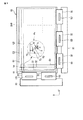
以下、本発明の第1実施形態に係る表示装置について、図面を参照して説明する。図1に示すように、本実施形態に係る表示装置は、マトリクス状に配置された複数の表示画素PXからなる表示部DYPを備えた液晶表示パネル10を有する液晶表示装置である。 Hereinafter, a display device according to a first embodiment of the present invention will be described with reference to the drawings. As shown in FIG. 1, the display device according to the present embodiment is a liquid crystal display device having a liquid crystal display panel 10 including a display unit DYP including a plurality of display pixels PX arranged in a matrix.
液晶表示パネル10は、アレイ基板12と、アレイ基板12に対向して配置された対向基板14と、アレイ基板12と対向基板14との間に挟持された液晶層5とを有している。アレイ基板12は、表示画素PXのそれぞれに配置された画素電極8を有している。対向基板14は、複数の画素電極8に対向するように配置された対向電極9を有している。
The liquid crystal display panel 10 includes an
液晶表示パネルの表示部DYPには、表示画素PXの配列する行に沿って配置された複数の走査線G(G1、G2、G3…)と、表示画素PXの配列する列に沿って配置された複数の信号線S(S1、S2、S3…)とが配置されている。 In the display unit DYP of the liquid crystal display panel, a plurality of scanning lines G (G1, G2, G3...) Arranged along the rows in which the display pixels PX are arranged and the columns in which the display pixels PX are arranged are arranged. A plurality of signal lines S (S1, S2, S3...) Are arranged.
各表示画素PXの、走査線Gと信号線Sとが交差する位置近傍には、信号線Sと画素電極8との間の接続を切り替える画素スイッチ7が配置されている。画素スイッチ7は、スイッチング素子として例えば薄膜トランジスタを有している。
A
画素スイッチ7のゲート電極7Gは、対応する走査線Gに電気的に接続されている(若しくは一体に形成されている)。画素スイッチ7のソース電極7Sは、対応する信号線Sに電気的に接続されている(若しくは一体に形成されている)。画素スイッチ7のドレイン電極7Dは、画素電極8に電気的に接続されている(若しくは一体に形成されている)。
The
画素スイッチ7のゲート電極7Gに所定のオン電圧が印加されると、ソース−ドレインパスが導通し、対応する信号線Sに印加された電圧信号が、画素電極8に供給される。対向電極9には、対向電極駆動回路(図示せず)により対向電圧が供給される。画素電極8に供給される電圧と対向電極9に供給される対向電圧との電位差により、液晶層5に含まれる液晶分子(図示せず)の配向状態が制御される。
When a predetermined on-voltage is applied to the
アレイ基板12の端部には、表示画素PXの駆動用ICが搭載された駆動基板22、32が接続されている。駆動基板22、32は、例えばTAB基板(COF(Chip On Film)、TCP(Tape Carrier Package)等)であって、フィルム上にICチップやLSIが搭載されたフレキシブル基板である。
駆動基板22には、走査線Gを順次駆動するゲートドライバGDが搭載されている。駆動基板32には、信号線Sを駆動するソースドライバSDが搭載されている。駆動基板22の液晶表示パネル10と反対側の端部には、ゲートドライバGDの制御信号および電源信号を供給する回路基板20が接続されている。駆動基板32の液晶表示パネル10の反対側の端部には、ソースドライバSDの制御信号および電源信号を供給する回路基板30が接続されている。
A gate driver GD that sequentially drives the scanning lines G is mounted on the
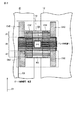
図2に示すように、駆動基板22は、アレイ基板12に接続された第1接続領域CN1と、回路基板20に接続された第2接続領域CN2とを有している。第1接続領域CN1は、異方性導電膜(ACF:Anisotropic Conductive Film)を介して、アレイ基板12に電気的に接続されている。第2接続領域CN2は、異方性導電膜を介して回路基板20に電気的に接続されている。
As shown in FIG. 2, the
第1接続領域CN1と第2接続領域CN2とは、それぞれ複数の接続ピンを有している。本実施形態に係る液晶表示装置では、第2接続領域CN2の接続ピンが並ぶ方向D1における中央部A1に配置された接続ピン(第2ピン)には、ゲートドライバGDに供給される制御信号あるいは電源信号が供給される配線GSに接続されている。第2接続領域CN2の方向D1における端部A2に配置された接続ピン(第4ピン)には、回路基板20のアース配線GNDが接続されている。
The first connection region CN1 and the second connection region CN2 each have a plurality of connection pins. In the liquid crystal display device according to the present embodiment, a control signal supplied to the gate driver GD or a connection pin (second pin) disposed in the central portion A1 in the direction D1 in which the connection pins of the second connection region CN2 are arranged is arranged. It is connected to a wiring GS to which a power signal is supplied. The ground wiring GND of the
第1接続領域CN1の方向D1における中央部A1に配置された接続ピン(第1ピン)には、ゲートドライバGDからの出力信号が供給される配線と、電源信号が供給される配線とが接続されている。第1接続領域CN1の方向D1における端部A2に配置された接続ピン(第3ピン)には、アレイ基板12のアース配線GNDが接続されている。
A connection pin (first pin) disposed in the central portion A1 in the direction D1 of the first connection region CN1 is connected to a wiring to which an output signal from the gate driver GD is supplied and a wiring to which a power supply signal is supplied. Has been. The ground wiring GND of the
さらに、駆動基板22は、第2接続領域の接続ピンのうちの回路基板20のアース配線GNDに接続された接続ピン(第4ピン)と、第1接続領域の接続ピンのうちのアレイ基板12のアース配線GNDに接続された接続ピン(第3ピン)とを接続するダミー配線WDを有している。
Further, the
なお、図2に示す場合では、第1接続領域CN1の端部A2に配置された接続ピン(第3ピン)、および、第2接続領域CN2の方向D1の端部A2に配置された接続ピン(第4ピン)は、アース配線GNDに接続されているが、これらの接続ピンがフローティング配線に接続されるようにしても良い。 In the case shown in FIG. 2, the connection pin (third pin) arranged at the end A2 of the first connection region CN1 and the connection pin arranged at the end A2 in the direction D1 of the second connection region CN2 The (fourth pin) is connected to the ground wiring GND, but these connection pins may be connected to the floating wiring.
すなわち、駆動基板22の第1接続領域CN1および第2接続領域CN2の接続ピンのうち、ゲートドライバGDの制御信号または電源信号の供給に使用されない接続ピンは、アース配線GNDおよびダミー配線WDによって接続されている。
That is, among the connection pins of the first connection region CN1 and the second connection region CN2 of the
このことによって、ゲートドライバGDの制御信号または電源信号の供給に使用される接続ピンと、ゲートドライバGDの制御信号または電源信号の供給に使用されない接続ピンとの、放熱性が略等しくなる。したがって、第1接続領域CN1および第2接続領域CN2が加熱された場合に、部分的に放熱性が高い部分や放熱性が低い部分が生じることを回避することができる。 As a result, the heat dissipation of the connection pins used for supplying the control signal or power signal of the gate driver GD and the connection pins not used for supplying the control signal or power signal of the gate driver GD becomes substantially equal. Therefore, when the first connection region CN1 and the second connection region CN2 are heated, it is possible to avoid the occurrence of a portion having a high heat dissipation property or a portion having a low heat dissipation property.
例えば、上記のような駆動基板22をアレイ基板12に接続する場合、駆動基板22の第1接続領域CN1あるいはアレイ基板12の接続領域に、異方性導電膜を貼り付ける。次に、第1接続領域CN1の接続ピンとアレイ基板12の接続領域の接続ピンとを位置合わせする。駆動基板22の第1接続領域CN1とアレイ基板12の接続領域とが位置合わせされた状態で、接続部分を所定の温度で加熱するとともに、アレイ基板12の厚さ方向に加圧して、駆動基板22をアレイ基板12に圧着させる。
For example, when the
本実施形態に係る表示装置では、上述のように、駆動基板22のゲートドライバGDの制御信号または電源信号の供給に使用される接続ピンと、ゲートドライバGDの制御信号または電源信号の供給に使用されない接続ピンとの、放熱性が略等しくなるように構成されているため、駆動基板22の圧着工程において駆動基板22の第1接続領域CN1および第2接続領域CN2が加熱された場合であっても、方向D1における中央部A1と端部A2とで接続ピンの放熱性が異なることが無くなる。
In the display device according to the present embodiment, as described above, the connection pins used for supplying the control signal or power signal of the gate driver GD of the
すなわち、本実施形態に係る表示装置によれば、圧着部材の浮きや剥がれを防止し、実装不良による製造歩留まりの低下を改善する表示装置を提供することができる。 That is, according to the display device according to the present embodiment, it is possible to provide a display device that prevents the crimping member from being lifted or peeled off, and that improves the reduction in manufacturing yield due to mounting defects.
なお、上記の説明では、駆動基板22について説明したが、駆動基板32についても同様に、ソースドライバSDの制御信号または電源信号の供給に使用されない接続ピンと、ソースドライバSDの制御信号または電源信号の供給に使用される接続ピンとの、放熱性が略等しくなるように構成されることによって、駆動基板32の浮きや剥がれによる圧着不良を防止することができる。
In the above description, the
次に、本発明の第2実施形態に係る表示装置について図面を参照して説明する。なお、以下の説明において、上述の第1実施形態に係る表示装置と同様の構成については、同一の符号を付して説明を省略する。 Next, a display device according to a second embodiment of the present invention will be described with reference to the drawings. In the following description, the same components as those of the display device according to the first embodiment described above are denoted by the same reference numerals and description thereof is omitted.
本実施形態に係る表示装置は、上述の第1実施形態に係る表示装置と同様に液晶表示パネル10を有している。液晶表示パネル10のアレイ基板12の端部には駆動基板22、32が接続されている。
The display device according to the present embodiment includes the liquid crystal display panel 10 as in the display device according to the first embodiment described above. Drive
図3に示すように駆動基板22は、第1接続領域CN1と第2接続領域CN2とを有している。第1接続領域CN1は、異方性導電膜を介して、アレイ基板12に電気的に接続されている。第2接続領域CN2は、異方性導電膜を介して回路基板20に電気的に接続されている。
As shown in FIG. 3, the
第1接続領域CN1と第2接続領域CN2とは、それぞれ複数の接続ピンを有している。本実施形態に係る液晶表示装置では、第2接続領域CN2の方向D1における中央部A1に配置された接続ピンには、配線GSからゲートドライバGDに供給される制御信号が供給される。第2接続領域CN2の方向D1における端部A2には、配線GSから電源信号が供給される接続ピン(第2ピン)が所定の間隔を置いて配置されている。 The first connection region CN1 and the second connection region CN2 each have a plurality of connection pins. In the liquid crystal display device according to the present embodiment, a control signal supplied from the wiring GS to the gate driver GD is supplied to the connection pins arranged in the central portion A1 in the direction D1 of the second connection region CN2. At the end A2 in the direction D1 of the second connection region CN2, connection pins (second pins) to which a power signal is supplied from the wiring GS are arranged at a predetermined interval.
第2接続領域CN2の端部A2において、電源信号が供給される接続ピンの間には、駆動信号も電源信号も供給されない接続ピン(第4ピン)が配置されている。なお、電源信号が供給される接続ピンは、方向D1における接続ピン同士の間隔が偏らないように端部A2に渡って配置されることが望ましく、さらには端部A2に渡って等間隔に配置されることが望ましい。 At the end A2 of the second connection region CN2, a connection pin (fourth pin) to which neither a drive signal nor a power signal is supplied is disposed between the connection pins to which the power signal is supplied. Note that the connection pins to which the power supply signal is supplied are desirably arranged over the end A2 so that the distance between the connection pins in the direction D1 is not biased, and further arranged at equal intervals over the end A2. It is desirable that
第1接続領域CN1の方向D1における中央部A1に配置された接続ピンには、配線GSからゲートドライバGDからの出力信号が供給される配線が接続されている。第1接続領域CN1の方向D1における端部A2には、電源信号が供給される配線が接続された接続ピン(第1ピン)が所定の間隔を置いて配置されている。 A wiring to which an output signal from the gate driver GD is supplied from the wiring GS is connected to the connection pin arranged in the central portion A1 in the direction D1 of the first connection region CN1. At the end A2 in the direction D1 of the first connection region CN1, connection pins (first pins) to which a wiring to which a power signal is supplied are connected are arranged at a predetermined interval.
第1接続領域CN1の端部A2において、電源信号が供給される接続ピンの間には、駆動信号も電源信号も供給されない接続ピン(第3ピン)が配置されている。なお、電源信号が供給される接続ピンは、方向D1における接続ピン同士の間隔が偏らないように端部A2に渡って配置されることが望ましく、さらには、端部A2に渡って等間隔に配置されることが望ましい。 At the end A2 of the first connection region CN1, a connection pin (third pin) to which neither a drive signal nor a power signal is supplied is disposed between connection pins to which a power signal is supplied. Note that the connection pins to which the power signal is supplied are preferably arranged over the end A2 so that the distance between the connection pins in the direction D1 is not biased, and further, the connection pins are equally spaced over the end A2. It is desirable to be arranged.
すなわち、駆動基板22の第1接続領域CN1および第2接続領域CN2の端部A2において、電源信号が供給される接続ピンが所定の間隔を置いて配置されている。このことによって、第1接続領域CN1および第2接続領域CN2が加熱された場合に、部分的に放熱性が高い部分や放熱性が低い部分が生じることを回避することができる。
That is, the connection pins to which the power supply signal is supplied are arranged at a predetermined interval in the end portion A2 of the first connection region CN1 and the second connection region CN2 of the
したがって、本実施形態に係る表示装置によれば、本実施形態に係る表示装置によれば、上述の第1実施形態に係る表示装置と同様に、圧着部材の浮きや剥がれを防止し、実装不良による製造歩留まりの低下を改善する表示装置を提供することができる。 Therefore, according to the display device according to the present embodiment, according to the display device according to the present embodiment, similarly to the display device according to the first embodiment described above, the crimping member is prevented from being lifted or peeled off, and the mounting failure is prevented. Thus, a display device can be provided which improves the reduction in manufacturing yield due to the above.
なお、上述の第1実施形態に係る表示装置の場合と同様に、上記の駆動基板22の構成は駆動基板32にも適用することが可能である。
Note that the configuration of the
次に、本発明の第3実施形態に係る表示装置について、図面を参照して以下に説明する。本実施形態に係る表示装置は、上述の第1実施形態に係る表示装置と同様に液晶表示パネル10を有している。液晶表示パネル10のアレイ基板12の端部には駆動基板22、32が接続されている。
Next, a display device according to a third embodiment of the present invention will be described below with reference to the drawings. The display device according to the present embodiment includes the liquid crystal display panel 10 as in the display device according to the first embodiment described above. Drive
図4に示すように駆動基板22は、第1接続領域CN1と第2接続領域CN2とを有している。第1接続領域CN1は、異方性導電膜を介して、アレイ基板12に電気的に接続されている。第2接続領域CN2は、異方性導電膜を介して回路基板20に電気的に接続されている。
As shown in FIG. 4, the
第1接続領域CN1と第2接続領域CN2とは、それぞれ複数の接続ピンを有している。本実施形態に係る液晶表示装置では、第2接続領域CN2の方向D1における中央部A1に配置された接続ピンには、配線GSからゲートドライバGDに供給される制御信号が供給される。第2接続領域CN2の方向D1における端部A2には、配線GSから電源信号が供給される接続ピン(第2ピン)が所定の間隔を置いて配置されている。 The first connection region CN1 and the second connection region CN2 each have a plurality of connection pins. In the liquid crystal display device according to the present embodiment, a control signal supplied from the wiring GS to the gate driver GD is supplied to the connection pins arranged in the central portion A1 in the direction D1 of the second connection region CN2. At the end A2 in the direction D1 of the second connection region CN2, connection pins (second pins) to which a power signal is supplied from the wiring GS are arranged at a predetermined interval.
第2接続領域CN2の端部A2において、電源信号が供給される接続ピン(第2ピン)の間には、回路基板20のアース配線GNDに接続された接続ピン(第4ピン)が配置されている。なお、電源信号が供給される接続ピンは、方向D1における接続ピン同士の間隔が偏らないように端部A2に渡って配置されることが望ましく、さらには端部A2に渡って等間隔に配置されることが望ましい。
In the end portion A2 of the second connection region CN2, a connection pin (fourth pin) connected to the ground wiring GND of the
第1接続領域CN1の方向D1における中央部A1に配置された接続ピンには、配線GSからゲートドライバGDからの出力信号が供給される配線が接続されている。第1接続領域CN1の方向D1における端部A2には、電源信号が供給される配線が接続された接続ピン(第1ピン)が所定の間隔を置いて配置されている。 A wiring to which an output signal from the gate driver GD is supplied from the wiring GS is connected to the connection pin arranged in the central portion A1 in the direction D1 of the first connection region CN1. At the end A2 in the direction D1 of the first connection region CN1, connection pins (first pins) to which a wiring to which a power signal is supplied are connected are arranged at a predetermined interval.
第1接続領域CN1の端部A2において、電源信号が供給される接続ピン(第1ピン)の間には、アレイ基板12のアース配線GNDに接続された接続ピン(第3ピン)が配置されている。なお、電源信号が供給される接続ピンは、方向D1における接続ピン同士の間隔が偏らないように端部A2に渡って配置されることが望ましく、さらには、端部A2に渡って等間隔に配置されることが望ましい。
At the end A2 of the first connection region CN1, a connection pin (third pin) connected to the ground wiring GND of the
さらに、駆動基板22は、第2接続領域CN2の端部A2に配置されたアース配線GNDに接続された接続ピン(第4ピン)と、第1接続領域CN1の端部A2に配置されたアース配線GNDに接続された接続ピン(第3ピン)とを接続するダミー配線WDを有している。
Further, the
すなわち、本実施形態では、駆動基板22の第1接続領域CN1および第2接続領域CN2の端部A2において、電源信号が供給される接続ピンが所定の間隔を置いて配置されている。
That is, in the present embodiment, the connection pins to which the power signal is supplied are arranged at predetermined intervals in the end portions A2 of the first connection region CN1 and the second connection region CN2 of the
さらに、駆動基板22の第1接続領域CN1および第2接続領域CN2の接続ピンのうち、ゲートドライバGDの制御信号または電源信号の供給に使用されない接続ピンは、アース配線GNDおよびダミー配線WDによって接続されている。
Further, of the connection pins of the first connection region CN1 and the second connection region CN2 of the
このことによって、第1接続領域CN1および第2接続領域CN2が加熱された場合に、部分的に放熱性が高い部分や放熱性が低い部分が生じることを回避することができる。 As a result, when the first connection region CN1 and the second connection region CN2 are heated, it can be avoided that a portion having a high heat dissipation property or a portion having a low heat dissipation property is generated.
したがって、本実施形態に係る表示装置によれば、上述の第1実施形態にかかる表示装置と同様に、圧着部材の浮きや剥がれを防止し、実装不良による製造歩留まりの低下を改善する表示装置を提供することができる。 Therefore, according to the display device according to the present embodiment, similarly to the display device according to the first embodiment described above, the display device that prevents the crimping member from being lifted or peeled off and improves the reduction in manufacturing yield due to mounting defects. Can be provided.
なお、この発明は、上記実施形態そのままに限定されるものではなく、実施段階ではその要旨を逸脱しない範囲で構成要素を変形して具体化できる。例えば、上記の実施形態では、表示装置として液晶表示装置について説明したが、TAB等の接続基板を加熱および加圧することにより回路基板を表示パネルに接続する表示装置であれば、液晶表示装置以外にも適用可能である。その場合であっても、上述の実施形態と同様の効果を得ることができる。 Note that the present invention is not limited to the above-described embodiment as it is, and can be embodied by modifying the constituent elements without departing from the scope of the invention in the implementation stage. For example, in the above-described embodiment, the liquid crystal display device has been described as the display device. However, other than the liquid crystal display device, any display device that connects the circuit board to the display panel by heating and pressurizing the connection board such as TAB can be used. Is also applicable. Even in that case, the same effect as the above-described embodiment can be obtained.
また、上記実施形態に開示されている複数の構成要素の適宜な組み合せにより種々の発明を形成できる。例えば、実施形態に示される全構成要素から幾つかの構成要素を削除してもよい。更に、異なる実施形態に亘る構成要素を適宜組み合せてもよい。 Further, various inventions can be formed by appropriately combining a plurality of constituent elements disclosed in the embodiment. For example, some components may be deleted from all the components shown in the embodiment. Furthermore, you may combine suitably the component covering different embodiment.
PX…表示画素、DYP…表示部、GD…ゲートドライバ、SD…ソースドライバ、CN1…第1接続領域、CN2…第2接続領域、10…表示パネル、20.30…駆動信号源、22、32…駆動基板(接続手段) PX ... display pixel, DYP ... display unit, GD ... gate driver, SD ... source driver, CN1 ... first connection region, CN2 ... second connection region, 10 ... display panel, 20.30 ... drive signal source, 22, 32 ... Drive board (connection means)
Claims (5)
前記複数の表示画素を駆動する駆動手段と、
前記表示パネルに制御信号を供給するとともに、接続手段によって前記表示パネルに取り付けられた駆動信号源と、を備え、
前記接続手段は、前記液晶表示パネルに電気的に接続された第1接続領域と、
前記駆動信号源に電気的に接続された第2接続領域と、
前記第1接続領域に配置された第1ピンと、前記第2接続領域に配置された第2ピンと、前記第1ピンと前記第2ピンとを接続するとともに前記駆動信号源から前記表示パネルの制御信号が供給される接続配線と、
前記第1接続領域に配置された第3ピンと、前記第2接続領域に配置された第4ピンと、前記第3ピンと前記第4ピンとを接続するダミー配線と、を備えている表示装置。 A display panel having a display unit composed of a plurality of display pixels;
Driving means for driving the plurality of display pixels;
A control signal is supplied to the display panel, and a drive signal source attached to the display panel by a connecting means,
The connection means includes a first connection region electrically connected to the liquid crystal display panel;
A second connection region electrically connected to the drive signal source;
The first pin disposed in the first connection region, the second pin disposed in the second connection region, the first pin and the second pin are connected, and a control signal of the display panel is transmitted from the drive signal source. Supplied connection wiring,
A display device, comprising: a third pin arranged in the first connection region; a fourth pin arranged in the second connection region; and a dummy wiring connecting the third pin and the fourth pin.
前記複数の表示画素を駆動する駆動手段と、
前記表示パネルに制御信号を供給するとともに、接続手段によって前記表示パネルに取り付けられた駆動信号源と、を備え、
前記接続手段は、前記表示パネルに電気的に接続された第1接続領域と、
前記駆動信号源に電気的に接続された第2接続領域と、
前記第1接続領域に配置された第1ピンと、前記第2接続領域に配置された第2ピンと、前記第1ピンと前記第2ピンとを接続するとともに前記駆動信号源から前記表示パネルの制御信号が供給される接続配線と、を備え、
前記第1ピンは前記第1接続領域において所定の間隔をおいて配置され、前記間隔に第3ピンが配置され、
前記第2ピンは前記第2接続領域において所定の間隔をおいて配置され、前記間隔に第4ピンが配置されている表示装置。 A display panel having a display unit composed of a plurality of display pixels;
Driving means for driving the plurality of display pixels;
A control signal is supplied to the display panel, and a drive signal source attached to the display panel by a connecting means,
The connection means includes a first connection region electrically connected to the display panel;
A second connection region electrically connected to the drive signal source;
The first pin disposed in the first connection region, the second pin disposed in the second connection region, the first pin and the second pin are connected, and a control signal of the display panel is transmitted from the drive signal source. Connecting wires to be supplied,
The first pins are arranged at a predetermined interval in the first connection region, and a third pin is arranged at the interval,
The display device in which the second pins are arranged at predetermined intervals in the second connection region, and the fourth pins are arranged at the intervals.
前記ダミー配線には、前記第3ピンおよび前記第4ピンを介して、前記表示パネルおよび前記駆動信号源のアース電極あるいはフロート電極に接続されている請求項3記載の表示装置。 The connection means further includes a dummy wiring that connects a third pin disposed in the first connection region and a fourth pin disposed in the second region,
The display device according to claim 3, wherein the dummy wiring is connected to the display panel and a ground electrode or a float electrode of the drive signal source via the third pin and the fourth pin.
前記第1駆動手段は、前記接続手段に配置されている請求項1乃至請求項5のいずれか1項記載の表示装置。 The driving means includes first driving means for driving the plurality of display pixels in units of rows, and second driving means for supplying a video signal to the display pixels selected by the first driving means,
The display device according to claim 1, wherein the first driving unit is disposed in the connection unit.
Priority Applications (3)
| Application Number | Priority Date | Filing Date | Title |
|---|---|---|---|
| JP2008177387A JP2010015114A (en) | 2008-07-07 | 2008-07-07 | Display |
| US12/496,459 US20100002181A1 (en) | 2008-07-07 | 2009-07-01 | Display device |
| TW098122661A TW201005896A (en) | 2008-07-07 | 2009-07-03 | Display device |
Applications Claiming Priority (1)
| Application Number | Priority Date | Filing Date | Title |
|---|---|---|---|
| JP2008177387A JP2010015114A (en) | 2008-07-07 | 2008-07-07 | Display |
Publications (2)
| Publication Number | Publication Date |
|---|---|
| JP2010015114A true JP2010015114A (en) | 2010-01-21 |
| JP2010015114A5 JP2010015114A5 (en) | 2010-07-22 |
Family
ID=41464094
Family Applications (1)
| Application Number | Title | Priority Date | Filing Date |
|---|---|---|---|
| JP2008177387A Pending JP2010015114A (en) | 2008-07-07 | 2008-07-07 | Display |
Country Status (3)
| Country | Link |
|---|---|
| US (1) | US20100002181A1 (en) |
| JP (1) | JP2010015114A (en) |
| TW (1) | TW201005896A (en) |
Cited By (1)
| Publication number | Priority date | Publication date | Assignee | Title |
|---|---|---|---|---|
| WO2016158747A1 (en) * | 2015-04-01 | 2016-10-06 | シャープ株式会社 | Flexible board for component mounting, and display device |
Citations (7)
| Publication number | Priority date | Publication date | Assignee | Title |
|---|---|---|---|---|
| JPS63177821A (en) * | 1987-01-19 | 1988-07-22 | 株式会社日立ホームテック | Cooking machine |
| JPH04301817A (en) * | 1991-03-29 | 1992-10-26 | Rohm Co Ltd | Liquid crystal display device and its production |
| JPH04355434A (en) * | 1991-05-31 | 1992-12-09 | Alps Electric Co Ltd | Liquid crystal display device |
| JPH0836189A (en) * | 1994-07-25 | 1996-02-06 | Casio Comput Co Ltd | Liquid crystal display module |
| JPH096252A (en) * | 1995-04-20 | 1997-01-10 | Canon Inc | Display device and mounting structure for its drive circuit |
| JPH11337966A (en) * | 1998-05-21 | 1999-12-10 | Sharp Corp | Semiconductor device |
| WO2000054098A1 (en) * | 1999-03-08 | 2000-09-14 | Matsushita Electric Industrial Co., Ltd. | Liquid crystal display and its inspecting method |
Family Cites Families (4)
| Publication number | Priority date | Publication date | Assignee | Title |
|---|---|---|---|---|
| JP4701069B2 (en) * | 2005-10-21 | 2011-06-15 | キヤノン株式会社 | Integrated display position detector |
| JP2007133016A (en) * | 2005-11-08 | 2007-05-31 | Toshiba Matsushita Display Technology Co Ltd | Liquid crystal display device |
| JP2008003194A (en) * | 2006-06-21 | 2008-01-10 | Toshiba Matsushita Display Technology Co Ltd | Substrate apparatus and method for manufacturing display element |
| JP2008130803A (en) * | 2006-11-21 | 2008-06-05 | Toshiba Matsushita Display Technology Co Ltd | Board device and substrate |
-
2008
- 2008-07-07 JP JP2008177387A patent/JP2010015114A/en active Pending
-
2009
- 2009-07-01 US US12/496,459 patent/US20100002181A1/en not_active Abandoned
- 2009-07-03 TW TW098122661A patent/TW201005896A/en unknown
Patent Citations (7)
| Publication number | Priority date | Publication date | Assignee | Title |
|---|---|---|---|---|
| JPS63177821A (en) * | 1987-01-19 | 1988-07-22 | 株式会社日立ホームテック | Cooking machine |
| JPH04301817A (en) * | 1991-03-29 | 1992-10-26 | Rohm Co Ltd | Liquid crystal display device and its production |
| JPH04355434A (en) * | 1991-05-31 | 1992-12-09 | Alps Electric Co Ltd | Liquid crystal display device |
| JPH0836189A (en) * | 1994-07-25 | 1996-02-06 | Casio Comput Co Ltd | Liquid crystal display module |
| JPH096252A (en) * | 1995-04-20 | 1997-01-10 | Canon Inc | Display device and mounting structure for its drive circuit |
| JPH11337966A (en) * | 1998-05-21 | 1999-12-10 | Sharp Corp | Semiconductor device |
| WO2000054098A1 (en) * | 1999-03-08 | 2000-09-14 | Matsushita Electric Industrial Co., Ltd. | Liquid crystal display and its inspecting method |
Cited By (1)
| Publication number | Priority date | Publication date | Assignee | Title |
|---|---|---|---|---|
| WO2016158747A1 (en) * | 2015-04-01 | 2016-10-06 | シャープ株式会社 | Flexible board for component mounting, and display device |
Also Published As
| Publication number | Publication date |
|---|---|
| TW201005896A (en) | 2010-02-01 |
| US20100002181A1 (en) | 2010-01-07 |
Similar Documents
| Publication | Publication Date | Title |
|---|---|---|
| JP5690916B2 (en) | Array substrate for display device | |
| US6853430B2 (en) | Display element driving apparatus and display using the same | |
| WO2010004875A1 (en) | Flexible substrate and electric circuit structure | |
| US20110169792A1 (en) | Display panel | |
| US9118324B2 (en) | Driver IC chip and pad layout method thereof | |
| KR102458382B1 (en) | Display apparatus and method of manufacturing the same | |
| JP2007121915A (en) | Display device | |
| US7483109B2 (en) | Space saving on peripheral rim outside display pixel region in display device | |
| TWI734062B (en) | Display panel and electronic device | |
| US20160349564A1 (en) | Display device | |
| US20080018849A1 (en) | Display element | |
| US20080119069A1 (en) | Board device and board | |
| KR102081129B1 (en) | Liquid Crystal Display Device | |
| US6791634B2 (en) | Display device having connecting pads crossing a spare line | |
| JP5512589B2 (en) | Driver integrated circuit chip power supply connection structure | |
| KR102120817B1 (en) | Driving integrated circuit pad unit and flat display panel having the same | |
| JP2008309825A (en) | Liquid crystal display | |
| JP2007178668A (en) | Flat display apparatus and manufacturing method therefor | |
| KR20040087452A (en) | Liquid crystal display module | |
| JP2010015114A (en) | Display | |
| JP2019008106A (en) | Array substrate and display panel including array substrate | |
| JP2012142341A (en) | Structure and method for wiring relay board and flexible board, and panel display device | |
| KR100766895B1 (en) | Display apparatus | |
| KR20080000369A (en) | Pad for liquid crystal display and liquid crystal display | |
| KR20080048690A (en) | Liquid crystal display device |
Legal Events
| Date | Code | Title | Description |
|---|---|---|---|
| A521 | Written amendment |
Free format text: JAPANESE INTERMEDIATE CODE: A523 Effective date: 20100603 |
|
| A621 | Written request for application examination |
Free format text: JAPANESE INTERMEDIATE CODE: A621 Effective date: 20100603 |
|
| A977 | Report on retrieval |
Free format text: JAPANESE INTERMEDIATE CODE: A971007 Effective date: 20101027 |
|
| A131 | Notification of reasons for refusal |
Free format text: JAPANESE INTERMEDIATE CODE: A131 Effective date: 20101102 |
|
| A02 | Decision of refusal |
Free format text: JAPANESE INTERMEDIATE CODE: A02 Effective date: 20110308 |