JP2010010234A - Device and method for inspecting workpiece - Google Patents
Device and method for inspecting workpiece Download PDFInfo
- Publication number
- JP2010010234A JP2010010234A JP2008165210A JP2008165210A JP2010010234A JP 2010010234 A JP2010010234 A JP 2010010234A JP 2008165210 A JP2008165210 A JP 2008165210A JP 2008165210 A JP2008165210 A JP 2008165210A JP 2010010234 A JP2010010234 A JP 2010010234A
- Authority
- JP
- Japan
- Prior art keywords
- wafer
- inspection object
- inspection
- inspected
- laser beam
- Prior art date
- Legal status (The legal status is an assumption and is not a legal conclusion. Google has not performed a legal analysis and makes no representation as to the accuracy of the status listed.)
- Granted
Links
Images


Abstract
Description
本発明は、被検査物の検査装置及び被検査物の検査方法に関する。特にウェーハ等の被検査物表面に光を照射し、被検査物表面に存在する異物や欠陥の状況を検査する被検査物の検査装置及び検査方法に関する。 The present invention relates to an inspection object inspection apparatus and an inspection object inspection method. In particular, the present invention relates to an inspection apparatus and inspection method for an inspection object that inspects the surface of an inspection object such as a wafer by irradiating light to the surface of the inspection object to check the state of foreign matter and defects.
ウェーハ等の被検査物を検査する検査装置の例として、特許文献1には被検査物のウェーハ表面を検査する被検査物の検査装置の技術が開示されている。
As an example of an inspection apparatus that inspects an inspection object such as a wafer,
特許文献1に開示されたウェーハの表面の検査装置の技術では、例えば、レーザー光源から出力するレーザービームがレンズ系によりレーザースポットSp(以下スポットSpと称する)となって被検査物のウェーハの表面に垂直又は斜めに投射され、ウェーハの移動に応じてウェーハの表面をスパイラル状に走査してウェーハの全面を走査する。そしてウェーハの表面に異物eや、スクラッチ傷,結晶欠陥(COP)等の欠陥が存在すると、レーザー光源から出力されたスポットSpが異物eやCOP等の欠陥によって広範囲な角度(方向)に散乱光Seを発生し、その散乱光Seの一部が集光レンズによって集光されて光電変換器である受光器の光電子増倍管(以下PMTと称する)に受光される。そしてPMTに入射した散乱光Seはここで電気信号に変換され、変換された電気信号(受光信号)をデータ処理することによって異物eやCOP等の欠陥の個数と大きさ、異物eや前記欠陥の位置を示す異物データを生成して、プリンタあるいはディスプレイ(図示せず)等にこの異物eや欠陥の状態をマップ表示するように構成されている例が示される。
In the technique of the wafer surface inspection apparatus disclosed in
また、特許文献2に開示されたウェーハ表面の検査装置では、例えば、静電容量センサで検出したウェーハのオリフラ部の両端部から、回転方向(θ方向)の位置座標のオフセット量を算出し、検出された異物の座標をオフセット量だけ補正する技術が開示されている。
Further, in the wafer surface inspection apparatus disclosed in
ところで、近年、半導体デバイス製造ラインや半導体ウェーハ製造ラインでは、光学式検査装置で検出された異物や欠陥の外観形状観察や成分分析がしばしば行われる。外観形状や成分分析の結果から、異物や欠陥の特徴付けと解析が行われ、発生箇所や発生原因を究明したり、或いは致命欠陥となるか否かなどが判別される。一般に、この外観形状観察や成分分析は、EDX(Energy Dispersive X-ray)分析装置を配設したSEM式外観検査装置によって行われる。しかし、SEM式外観検査装置は、高分解能ではあるものの視野が狭いため、測定対象の異物や欠陥の位置座標がずれた場合には、それを発見するのに多大な時間を要することになる。そのため、光学式検査装置では異物や欠陥の高感度検出のほかに、異物や欠陥の高精度な座標と(座標精度)、他の分析装置との間で適正にマッチングの取れる異物や欠陥の位置情報データが求められている。 Incidentally, in recent years, in semiconductor device manufacturing lines and semiconductor wafer manufacturing lines, appearance shape observation and component analysis of foreign matters and defects detected by an optical inspection apparatus are often performed. From the appearance shape and component analysis results, characterization and analysis of foreign matter and defects are performed to determine the location and cause of occurrence, or to determine whether or not a fatal defect occurs. In general, the appearance observation and component analysis are performed by an SEM appearance inspection apparatus provided with an EDX (Energy Dispersive X-ray) analyzer. However, although the SEM visual inspection apparatus has a high resolution but a narrow field of view, it takes a lot of time to find out if the position coordinates of the foreign object or defect to be measured are shifted. Therefore, in addition to high-sensitivity detection of foreign matter and defects, optical inspection equipment has high-accuracy coordinates (coordinate accuracy) of foreign matter and defects, and positions of foreign matters and defects that can be properly matched with other analyzers. Information data is required.
しかしながら、上記従来の検査技術では、被検査物から検出された異物や欠陥の座標精度については配慮がなされておらず、ウェーハ搬送機構等によってステージへの設置位置がずれた場合には、被検査物の異物や欠陥は位置座標がずれて検出される虞がある。 However, in the above conventional inspection technology, no consideration has been given to the coordinate accuracy of the foreign matter or defect detected from the inspection object, and if the installation position on the stage is shifted by the wafer transfer mechanism, etc. There is a risk that foreign objects and defects of objects may be detected with positional coordinates shifted.
また、上記従来の検査技術では、現在主流となっているVノッチの場合、検出する両端が接近しているためθズレの検出精度が低下し、θズレの補正精度も低下する。また、ウェーハの回転方向(θ方向)のみの補正であるため、上記と同様、ウェーハ搬送機構等でステージへの設置位置が回転方向(θ方向)以外の方向にずれた場合には、被検査物の異物や欠陥は位置座標がずれて検出される虞がある。特に、被検査物を裏面非接触で検査するために用いられるエッジグリップタイプのステージ等においては、被検査物をエッジ部の僅かな接触面で支持させるため、ウェーハをステージに設置する際に位置ずれを生じやすい。ウェーハ搬送機構の制御誤差の他に、ステージでの位置ずれが加算されるため、検出される異物や欠陥の座標精度を維持することが極めて困難である。 In the conventional inspection technique, in the case of V notches, which are currently in the mainstream, both ends to be detected are close to each other, so that the θ shift detection accuracy is lowered and the θ shift correction accuracy is also lowered. In addition, since the correction is only for the rotation direction (θ direction) of the wafer, if the installation position on the stage is shifted in a direction other than the rotation direction (θ direction) by the wafer transfer mechanism or the like, the inspection target There is a risk that foreign objects and defects of objects may be detected with positional coordinates shifted. In particular, in an edge grip type stage used for inspecting an object to be inspected in a non-contact manner on the back surface, the object to be inspected is supported by a slight contact surface of the edge portion. Misalignment is likely to occur. In addition to the control error of the wafer transfer mechanism, the positional deviation on the stage is added, so it is extremely difficult to maintain the coordinate accuracy of the detected foreign matter or defect.
ところで、一般にウェーハの搬送機構系などには、搬送毎に大きさの異なるランダム誤差を含んでいる。同一ウェーハを用いたとしてもステージへの設置位置は搬送毎に微妙に変動し、同一の設置位置には再現されない。そのため、より高い座標精度が求められる超微小の異物や欠陥の検出においては、被検査物の検査毎に異物や欠陥の位置座標が変動し、位置座標が定まらない、同一ウェーハにおける座標の再現性が得られないという、座標精度上の課題を生じる。この搬送系のランダム誤差は、光学式検査装置に限らず、例えば外観検査装置などの他の検査装置も同様に有するものであり、装置個々においてその状態やレベルは異なる。光学式検査装置の異物や欠陥の位置情報データを、他の分析装置のステージにマッチングさせることを困難とする原因の一つでもある。 Incidentally, in general, a wafer transfer mechanism system and the like include random errors having different sizes for each transfer. Even if the same wafer is used, the installation position on the stage varies slightly with each transfer, and is not reproduced at the same installation position. For this reason, in the detection of ultra-fine foreign objects and defects that require higher coordinate accuracy, the position coordinates of the foreign objects and defects fluctuate every time the inspection object is inspected, and the position coordinates cannot be determined. This causes a problem in the accuracy of coordinates that cannot be obtained. This random error in the transport system is not limited to the optical inspection apparatus, but is also included in other inspection apparatuses such as an appearance inspection apparatus, and the state and level of each apparatus are different. This is also one of the causes that make it difficult to match the position information data of the foreign matter or defect of the optical inspection device to the stage of another analysis device.
本発明の一つの目的は、ステージに対する被検査物の設置位置に影響を受けることなく、異物や欠陥の座標を高精度で検出できる検査装置およびその方法を提供することにある。 One object of the present invention is to provide an inspection apparatus and method that can detect the coordinates of a foreign object or a defect with high accuracy without being affected by the installation position of the inspection object with respect to the stage.
また本発明の他の目的は、一つの検査装置で検出した異物や欠陥の位置座標を、その他の分析装置のステージに適正にマッチングさせることができる検査装置およびその方法を提供することにある。 Another object of the present invention is to provide an inspection apparatus and method capable of appropriately matching the position coordinates of a foreign object or defect detected by one inspection apparatus with the stage of another analysis apparatus.
本発明は、前記被検査物に照射されたレーザービームによって前記被検査物の表面から放射される光を検出する複数の検出器を有し、前記複数の検出器で検出された光の検出信号に基づいて、前記被検査物の表面の形状によって、区分される領域を判別し、前記複数の検出器で検出された光の検出信号に基づいて、検査を行う構成としたことを1つの特徴とする。 The present invention has a plurality of detectors for detecting light emitted from the surface of the inspection object by a laser beam applied to the inspection object, and detection signals of light detected by the plurality of detectors One feature is that a region to be classified is discriminated based on the shape of the surface of the object to be inspected, and inspection is performed based on detection signals of light detected by the plurality of detectors. And
以下に、具体的な本発明の特徴を列挙する。 Specific features of the present invention are listed below.
本発明の被検査物の検査装置は、被検査物にレーザービームを照射する投光光学系と、前記被検査物をテーブルに載置して前記テーブルを回転させる回転駆動機構と、前記回転駆動機構を前記被検査物の移送方向に移動させる移動機構と、前記被検査物に照射されたレーザービームによって前記被検査物の表面から放射される光を検出する複数の検出器と、前記複数の検出器で検出された光の検出信号に基づいて前記被検査物の表面の平坦領域と前記被検査物外周部のベベル部に該当する境界位置を判別し、被検査物を検査するデータ処理装置とを備えて構成したことを特徴とする。 The inspection object inspection apparatus according to the present invention includes a projection optical system that irradiates a laser beam to the inspection object, a rotation drive mechanism that rotates the table by placing the inspection object on a table, and the rotation drive. A moving mechanism for moving a mechanism in a direction in which the inspection object is transferred; a plurality of detectors for detecting light emitted from the surface of the inspection object by a laser beam applied to the inspection object; A data processing device for inspecting an inspection object by determining a boundary position corresponding to a flat area on the surface of the inspection object and a bevel portion of the outer periphery of the inspection object based on a detection signal of light detected by a detector It is characterized by comprising.
また本発明の被検査物の検査装置は、被検査物にレーザービームを照射する投光光学系と、前記被検査物をテーブルに載置して前記テーブルを回転させる回転駆動機構と、前記回転駆動機構を前記被検査物の移送方向に移動させる移動機構と、前記回転駆動機構と前記移動機構の位置座標情報を発信する駆動制御器と、前記被検査物に照射されたレーザービームによって前記被検査物の表面から放射される光を検出する複数の検出器と、前記複数の検出器で検出された光の検出信号に基づいて前記被検査物外周部のベベル部に該当する境界位置を判別し、前記駆動制御器からの位置座標情報と関連付けて、前記被検査物周方向の前記境界位置を出力し、被検査物を検査するデータ処理装置とを備えて構成したことを特徴とする。 The inspection apparatus for an inspection object according to the present invention includes a light projecting optical system that irradiates the inspection object with a laser beam, a rotation drive mechanism that rotates the table by placing the inspection object on a table, and the rotation A moving mechanism that moves the driving mechanism in the transfer direction of the object to be inspected, a drive controller that transmits position coordinate information of the rotational driving mechanism and the moving mechanism, and a laser beam irradiated to the object to be inspected. A plurality of detectors for detecting light emitted from the surface of the inspection object, and a boundary position corresponding to the bevel portion of the outer peripheral portion of the inspection object based on detection signals of light detected by the plurality of detectors And a data processing device that outputs the boundary position in the circumferential direction of the inspection object in association with the position coordinate information from the drive controller and inspects the inspection object.
また本発明の被検査物の検査装置は、被検査物にレーザービームを照射する投光光学系と、前記被検査物をテーブルに載置して前記テーブルを回転させる回転駆動機構と、前記回転駆動機構を前記被検査物の移送方向に移動させる移動機構と、前記回転駆動機構と前記移動機構の位置座標情報を発信する駆動制御器と、前記被検査物に照射されたレーザービームによって前記被検査物の表面から放射される光を検出する複数の検出器と、前記複数の検出器で検出された光の検出信号に基づいて前記被検査物外周部のベベル部に該当する境界位置を判別して、前記駆動制御器からの位置座標情報との関連付けによって前記被検査物周方向の前記境界位置を出力し、該被検査物周方向の境界位置に基づいて、前記被検査物の略中心座標を出力し、被検査物を検査するデータ処理装置とを備えて構成したことを特徴とする。 The inspection apparatus for an inspection object according to the present invention includes a light projecting optical system that irradiates the inspection object with a laser beam, a rotation drive mechanism that rotates the table by placing the inspection object on a table, and the rotation A moving mechanism that moves the driving mechanism in the transfer direction of the object to be inspected, a drive controller that transmits position coordinate information of the rotational driving mechanism and the moving mechanism, and a laser beam irradiated to the object to be inspected. A plurality of detectors for detecting light emitted from the surface of the inspection object, and a boundary position corresponding to the bevel portion of the outer peripheral portion of the inspection object based on detection signals of light detected by the plurality of detectors Then, the boundary position in the circumferential direction of the inspection object is output in association with the position coordinate information from the drive controller, and the approximate center of the inspection object is based on the boundary position in the circumferential direction of the inspection object Output coordinates, Characterized by being configured to include a data processing apparatus for inspecting a test object.
本発明の被検査物の検査方法は、被検査物を載置したテーブルを回転させて、該被検査物にレーザービームを照射して検査する被検査物の検査方法において、前記被検査物に照射されたレーザービームによって前記被検査物の表面から放射される光を複数の検出器で検出し、前記複数の検出器で検出された光の検出信号に基づいて演算処理するデータ処理装置によって前記被検査物の表面の平坦領域と前記被検査物外周部のベベル部に該当する境界位置を判別し、被検査物を検査することを特徴とする。 The inspection method for an inspection object according to the present invention is the inspection object inspection method in which the table on which the inspection object is mounted is rotated and the inspection object is inspected by irradiating the inspection object with a laser beam. The light emitted from the surface of the object to be inspected by the irradiated laser beam is detected by a plurality of detectors, and the data processing device performs arithmetic processing based on detection signals of the lights detected by the plurality of detectors. The inspection object is inspected by discriminating a boundary position corresponding to a flat region on the surface of the inspection object and a bevel portion of the outer periphery of the inspection object.
また本発明の被検査物の検査方法は、被検査物を載置したテーブルを回転させて、該被検査物にレーザービームを照射して検査する被検査物の検査方法において、前記被検査物に照射されたレーザービームによって前記被検査物の表面から放射される光を複数の検出器で検出し、前記複数の検出器で検出された光の検出信号に基づいて演算処理するデータ処理装置によって前記被検査物の表面の平坦領域と前記被検査物外周部のベベル部に該当する境界位置を前記テーブルの座標情報と関連付けて判別し、前記被検査物の境界位置分布を出力し、被検査物を検査することを特徴とする。 Further, the inspection method for an inspection object according to the present invention is the inspection object inspection method in which the table on which the inspection object is placed is rotated, and the inspection object is irradiated with a laser beam. By a data processing device that detects light emitted from the surface of the object to be inspected by a laser beam irradiated on a plurality of detectors and performs arithmetic processing based on detection signals of the lights detected by the plurality of detectors A boundary position corresponding to a flat area on the surface of the inspection object and a bevel portion of the outer periphery of the inspection object is determined in association with the coordinate information of the table, and a boundary position distribution of the inspection object is output, It is characterized by inspecting an object.
また本発明の被検査物の検査方法は、被検査物を載置したテーブルを回転させて、該被検査物にレーザービームを照射して検査する被検査物の検査方法において、前記被検査物に照射されたレーザービームによって前記被検査物の表面から放射される光を複数の検出器で検出し、前記複数の検出器で検出された光の検出信号に基づいて演算処理するデータ処理装置によって前記被検査物の表面の平坦領域と前記被検査物外周部のベベル部に該当する境界位置を前記テーブルの座標情報と関連付けて判別して前記被検査物の境界位置分布を出力し、この境界位置分布に基づいて前記被検査物の略中心座標を出力し、被検査物を検査することを特徴とする。 Further, the inspection method for an inspection object according to the present invention is the inspection object inspection method in which the table on which the inspection object is placed is rotated, and the inspection object is irradiated with a laser beam. By a data processing device that detects light emitted from the surface of the object to be inspected by a laser beam irradiated on a plurality of detectors and performs arithmetic processing based on detection signals of the lights detected by the plurality of detectors The boundary position corresponding to the flat area of the surface of the inspection object and the bevel portion of the outer periphery of the inspection object is determined in association with the coordinate information of the table, and the boundary position distribution of the inspection object is output, and this boundary A substantially central coordinate of the inspection object is output based on the position distribution, and the inspection object is inspected.
本発明の一つの様態によれば、ステージに対する被検査物の設置位置に影響を受けることなく、異物や欠陥の座標を高精度で検出すことができる。 According to one aspect of the present invention, the coordinates of a foreign object or a defect can be detected with high accuracy without being affected by the installation position of the inspection object with respect to the stage.
本発明の他の様態によれば、一つの検査装置で検出した異物や欠陥の位置座標を、その他の分析装置のステージに、適正にマッチングさせることができる。 According to another aspect of the present invention, the position coordinates of a foreign object or a defect detected by one inspection apparatus can be appropriately matched with the stage of another analysis apparatus.
本発明の実施例である被検査物の検査装置及び被検査物の検査方法について、図面を参照して以下に説明する。 An inspection object inspection apparatus and an inspection object inspection method according to embodiments of the present invention will be described below with reference to the drawings.
本発明の実施例に記載する、被検査物の検査装置及び検査方法に適用される被検査物とは、例えばシリコンや化合物半導体などの半導体ウェーハ,絶縁物ウェーハ(例えば、サファイア,石英,ガラス,セラミックを素材とした基板)などの平板状基板である。 Examples of the inspection object and inspection method for the inspection object described in the embodiments of the present invention include semiconductor wafers such as silicon and compound semiconductors, insulator wafers (for example, sapphire, quartz, glass, A flat substrate such as a substrate made of ceramic.
以下に記載する実施例では、半導体ウェーハを被検査物として適用した、本発明の一実施例である被検査物の検査方法及び検査装置について説明する。 In the embodiments described below, an inspection object inspection method and inspection apparatus according to an embodiment of the present invention, in which a semiconductor wafer is applied as an inspection object, will be described.
本発明の一実施例であるウェーハ表面の検査装置では、レーザービームをウェーハの略中心部から外周部へと照射しながら、ウェーハ表面から発せられる散乱光を受光し、この受光した散乱光に基づいてウェーハ表面を検査する。 In the wafer surface inspection apparatus according to one embodiment of the present invention, while irradiating a laser beam from the substantially central portion to the outer peripheral portion of the wafer, the scattered light emitted from the wafer surface is received, and based on the received scattered light. Inspect the wafer surface.
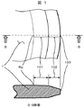
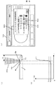
図1はウェーハ外周部の断面を示したものであるが、ウェーハ検査装置ではレーザービームがウェーハ外周部のエッジロールオフ101やベベル102(エッジ部)へ差し掛ると、ウェーハ表面から強い回折光が射出され、検出器のノイズ信号を増大させたり、更には検出器にダメージを与えて、検出感度を低下させる。そのため、通常のウェーハ検査装置では、回折光の影響でノイズ信号が高くなる領域を非検査領域とし、ウェーハ表面の検査領域から除外することによって、回折光の障害を回避している。 FIG. 1 shows a cross section of the wafer outer peripheral portion. In the wafer inspection apparatus, when the laser beam hits the edge roll-off 101 or the bevel 102 (edge portion) of the wafer outer peripheral portion, strong diffracted light is emitted from the wafer surface. As a result, the noise signal of the detector is increased, or the detector is damaged, and the detection sensitivity is lowered. For this reason, in a normal wafer inspection apparatus, a region where the noise signal is increased due to the influence of diffracted light is set as a non-inspection region, and is excluded from the inspection region on the wafer surface, thereby avoiding the obstacle of diffracted light.
しかしながら、回折光の影響でノイズ信号が高くなるウェーハ外周部の領域を、ウェーハ表面の検査領域から除外すると、この領域から発せられる散乱光が受光できなくなるため、前記領域のウェーハの表面に付着した異物や表面に生じた欠陥の情報を得ることができない。また、ウェーハ外周部を検査領域から除外するため、図1に示すエッジロールオフ101やベベル102(エッジ部)の領域を検出することもできなくなる。 However, if the wafer peripheral area where the noise signal is high due to the influence of diffracted light is excluded from the inspection area on the wafer surface, the scattered light emitted from this area can no longer be received, so that it adheres to the wafer surface in the area. It is not possible to obtain information on foreign matters or defects generated on the surface. Further, since the outer peripheral portion of the wafer is excluded from the inspection region, the edge roll-off 101 and the bevel 102 (edge portion) region shown in FIG. 1 cannot be detected.
そこで、本発明の一実施例である被検査物の検査装置では、ウェーハ表面に照射したレーザービームによって、ウェーハ表面から発せられる散乱光を検出する検出器(受光器)を複数個設置し、ウェーハのベベル102(エッジ部)から発せられる強い回折光が常に略同一の方向(方位)へ放射される特性を利用して回折光の障害を回避する。この複数の検出器(受光器)の中から、ウェーハのベベル102(エッジ部)で発生する回折光の影響を受けない方向(方位,仰角)に配置した検出器(受光器)を選択して散乱光を受光することで、ウェーハの表面に付着した異物や表面に生じた欠陥の情報を、ウェーハ表面の全体に亘って採取可能に構成したものである。 Therefore, in the inspection apparatus for an object to be inspected according to an embodiment of the present invention, a plurality of detectors (light receivers) for detecting scattered light emitted from the wafer surface by a laser beam irradiated on the wafer surface are installed, and the wafer The obstacle of the diffracted light is avoided by utilizing the characteristic that strong diffracted light emitted from the bevel 102 (edge portion) is always radiated in substantially the same direction (orientation). From these multiple detectors (photodetectors), select a detector (photoreceiver) arranged in a direction (azimuth, elevation) that is not affected by the diffracted light generated at the wafer bevel 102 (edge portion). By receiving the scattered light, information on foreign matters attached to the wafer surface and defects generated on the surface can be collected over the entire wafer surface.
また、本発明の一実施例である被検査物の検査装置では、ウェーハ表面に照射したレーザービームによって、ウェーハ表面から発せられる散乱光を検出する検出器(受光器)を複数個設置し、複数の検出器(受光器)で受光した散乱光の検出信号に基づいて演算処理することにより、レーザービームが照射するウェーハ表面の平坦な平面領域と、該平面領域から外れたウェーハ外周部のエッジロールオフ101やベベル102(エッジ部)に該当する所定領域との境界位置を判別可能に構成したものである。 In the inspection apparatus for an inspection object according to an embodiment of the present invention, a plurality of detectors (light receivers) for detecting scattered light emitted from the wafer surface by a laser beam irradiated on the wafer surface are installed. A flat plane area on the wafer surface irradiated with the laser beam and an edge roll on the outer periphery of the wafer outside the plane area by performing arithmetic processing based on the detection signal of the scattered light received by the detector (receiver) The boundary position with a predetermined area corresponding to the off 101 or the bevel 102 (edge portion) can be determined.
さらに、本発明の一実施例である被検査物の検査装置では、ウェーハ表面に照射したレーザービームによって、ウェーハ表面から発せられる散乱光を検出する検出器(受光器)を複数個設置し、複数の検出器(受光器)で受光した散乱光の検出信号に基づく演算処理にて、所定領域の境界位置を判別し、当該境界位置から表面検査されたウェーハの複数の基準位置を算出し、検出された異物や欠陥の座標位置を、当該基準位置に基づいて補正可能に構成したものである。 Further, in the inspection object inspection apparatus according to an embodiment of the present invention, a plurality of detectors (light receivers) for detecting scattered light emitted from the wafer surface by a laser beam irradiated on the wafer surface are installed. In the calculation process based on the detection signal of the scattered light received by the detector (receiver), the boundary position of the predetermined area is determined, and multiple reference positions of the surface-inspected wafer are calculated and detected from the boundary position The coordinate position of the foreign matter or defect thus made can be corrected based on the reference position.
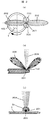
図2から図6を用いて、本発明の一実施例である被検査物の検査装置を詳細に説明すると、まず、図2は被検査物である半導体ウェーハ1と、この半導体ウェーハ1に照射するレーザービーム204の状況と、レーザービーム204の照射によってウェーハ1のベベル102(エッジ部)で生じる強い回折光202,弱い回折光203の強度と、レーザービーム204の照射によってウェーハ1表面の異物から発生する散乱光Seを示した概念図である。
The inspection object inspection apparatus according to an embodiment of the present invention will be described in detail with reference to FIGS. 2 to 6. First, FIG. 2 shows a
そして、図2(a)はウェーハ1のベベル102(エッジ部)で生じる強い回折光202と弱い回折光203を上方から示した上面図、図2(b)はウェーハ1のベベル102(エッジ部)で生じる強い回折光202を側面から示した側面図、図2(c)はウェーハ1表面に存在する異物又は欠陥(COP,積層欠陥,スクラッチ,クラック等)205から発生する散乱光Seの状態を示した説明図である。
2A is a top view showing the strong diffracted light 202 and the weak diffracted light 203 generated at the bevel 102 (edge part) of the
図2(a)(b)に示されるレーザービーム204によって形成されるレーザースポット201は、ウェーハ1表面の略中心から、半径(r)方向の外周端部に向かって走査される。レーザースポット201が、ウェーハ1のエッジロールオフ101領域からベベル102領域へと進むに従い、回折光は次第に大きくなり、ベベル102領域ではウェーハ1の直径方向に強い回折光202が生じ、ウェーハ1の接線方向には弱い(小さい)回折光203が生じる。図2(b)は、レーザービーム204がウェーハ1のベベル102領域に照射された際の、ベベル102で生じる強い回折光202を側面から見たものであり、レーザースポット201内のレーザービーム204がウェーハ1のベベル102で回折し、強い回折光202がウェーハの半径方向に向かって形成される。
A
この強い回折光202は、ウェーハ1表面に照射されるレーザースポット201の照射位置が一定に制御され、ウェーハ1が矢印で示す円周方向に回転しながら、所定の一定方位へ直線移動することにより、常にウェーハ1の直径方向に発生する。
This intense diffracted light 202 is controlled by the irradiation position of the
したがって、後述する検出器(受光器)に対して、ベベル102領域で発生するこの強い回折光202は、常に同じ方向(方位,仰角)に位置する。この強い回折光202の影響によって、ウェーハ1表面に存在する異物又は欠陥205から発生する散乱光Seは、強い回折光202に起因するノイズ信号の中に埋れてしまい、散乱光Seの望ましい検出信号を得ることが困難となる。
Therefore, the strong diffracted light 202 generated in the
図2(c)は、ウェーハ1の表面に照射されるレーザービーム204からなるレーザースポット201が、ウェーハ表面の平坦な平面領域を走査している状態を示したものである。ウェーハ1表面に存在する異物又は欠陥205の上をレーザースポット201が走査すると、異物又は欠陥205から、そのの種類に応じた散乱光を放出する。微細な異物の場合には、広範囲な角度(方向)に散乱光Seが発生する。COPやスクラッチなどの構造欠陥の場合には、上方に指向性を持った散乱光が放出される。
FIG. 2C shows a state where a
ところが、ウェーハ1表面に照射されるレーザービーム204のレーザースポット201が、ウェーハ1端部のベベル102領域に位置する場合には、前述のベベル102領域で生じる強い回折光202の影響によって、ノイズ信号が増大する。したがって、このウェーハ1表面のベベル102領域に異物又は欠陥205が存在したとしても、このノイズ信号の中に異物又は欠陥205から発生した散乱光Seによる検出信号が埋れてしまい、ベベル102領域の異物又は欠陥205を検出することができないことになる。
However, when the
そこで、本発明の実施例である被検査物の検査装置では、以下の構成によってベベル102領域からの強い回折光202によるノイズの影響を排除或いは低減して、ウェーハ1表面の異物又は欠陥205で発生する散乱光Seを効果的に検出できるようにしている。
Therefore, in the inspection object inspection apparatus according to the embodiment of the present invention, the influence of noise caused by the strong diffracted light 202 from the
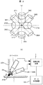
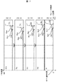
図4は本発明の一実施例である被検査物の検査装置を構成する検出系の簡略構成図であり、図3は図4に示した検査装置を構成する検出器の概略を示すものであって、図3(a)は検出器の配置状況を示した上面図、図3(b)はウェーハ1表面で生じた散乱光を検出器で検出した際の、検出信号の処理内容を示す概略図である。
FIG. 4 is a simplified configuration diagram of a detection system constituting an inspection apparatus for an inspection object according to an embodiment of the present invention, and FIG. 3 shows an outline of a detector constituting the inspection apparatus shown in FIG. 3A is a top view showing the arrangement of detectors, and FIG. 3B shows processing contents of detection signals when scattered light generated on the surface of the
図3及び図4を用いて、本発明の一実施例であるウェーハ1表面を検査するウェーハ検査装置の構成を説明する。図3(a)には、ウェーハ1からの散乱光を検出する光電子増倍管(PMT)等からなる高角度用(高仰角用)の検出器(受光器)371〜374、及び高角度用より低角側の散乱光を検出する低角度用(低仰角用)の検出器(受光器)381〜386を、それぞれ上方から見た配置の一例を示している。また、図3(b)は、図3(a)に示した高角度用検出器371〜374及び低角度用検出器381〜386の一部分を、側方から見た配置の一例を示している。
The configuration of a wafer inspection apparatus for inspecting the surface of the
高角度用検出器371〜374は、ウェーハ1表面に照射したレーザービーム204によって異物又は欠陥205から放出された散乱光Seのうち、ウェーハ1表面から約50〜70°の角度(仰角)に沿って入射するように配置されている。高角度用検出器371〜374は、上方から見た場合、円周方向に相互に略90°ずつそれぞれの配置方向(方位)を異ならせて円周方向に4個配置している。
The
同様に低角度用検出器381〜386は、ウェーハ1表面に照射したレーザービーム204によって異物又は欠陥205から放出された散乱光Seのうち、ウェーハ1表面から約20〜40°の角度(仰角)に沿って入射するように配置されている。低角度用検出器381〜386は、上方から見た場合、円周方向に相互に略60°ずつそれぞれの配置方向(方位)を異ならせて円周方向に6個配置している。
Similarly, the low-
これらの高角度用検出器371〜374、及び低角度用検出器381〜386のうち、レーザービーム204の照射によってウェーハ1のベベル102領域で生じた強い回折光202の大きな影響を受ける検出器は、ウェーハ1の直径方向に沿って配置された高角度用検出器372及び374であり、次に強い回折光202の影響を受ける検出器は、低角度用検出器384及び385、並びに低角度用検出器381及び382である。
Among these high-
また、前記した強い回折光202による影響が少ない検出器は、ウェーハ1の直径方向とは直角に配置された、即ちウェーハ1の接線方向と平行する位置関係に配置された高角度用検出器371及び373である。また、強い回折光202による次に影響が少ない検出器は、低角度用検出器383及び386である。
In addition, the above-described detector that is less affected by the strong diffracted light 202 is arranged at a right angle to the diameter direction of the
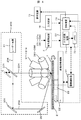
図4は、本実施例のウェーハ表面検査装置の概略構成を示したものである。ウェーハ表面検査装置は、ウェーハ1を載置させるテーブル21と、テーブル21を回転させるスピンドルモータ等からなる回転駆動機構23と、このテーブル21と回転駆動機構23を搭載してウェーハ1を所定の略直線方向に移動させる直線移動機構22(進退駆動機構)と、投光光学系400と、回転駆動機構23と直線移動機構22を制御する駆動制御器51と、信号処理装置4と、データ処理装置52と、ディスプレイ等からなる表示装置75を備えて構成される。回転テーブル21に載置された検査対象となる被検査物のウェーハ1は、所定の回転速度に制御され、直線移動機構22により略中心からベベル102方向に向かって、所定方位へ直線移動する。
FIG. 4 shows a schematic configuration of the wafer surface inspection apparatus of the present embodiment. The wafer surface inspection apparatus includes a table 21 on which the
このウェーハ1の上部に配置された投光光学系400は、2つの投光光学系を備えて構成されている。第1の投光光学系では、レーザー発振器を備えたレーザー光源31から出力したレーザービーム204を、下方へと光路を変更するミラー331(光路切換機構)によって反射し、鉛直方向下方にレーザースポットSp(以下スポットSpと称する)を形成してウェーハ1の表面に略垂直に投射される(垂直照射)。
The light projecting
第2の投光光学系では、レーザー光源31から出力されたレーザービーム204の光路から、光路を変更するミラー331を二点鎖線で示した垂直方向の上方の位置に移動させ、光路の延長線上に配置された第2の投光光学系を構成するミラー332によって、レーザービーム204を鉛直方向下方に反射させる。次いで、この反射したレーザービーム204を、ウェーハ1表面への入射角を制御するミラー35(入射角制御機構)によって反射し、レーザースポット201をウェーハ1表面に所定の入射角で投射する(斜方照射)。
In the second light projecting optical system, the
上記の垂直照射のレーザースポット201、又は斜方照射のレーザースポット201は、回転駆動機構23及び直線移動機構22の駆動によるウェーハ1の移動によって、ウェーハ1の表面を走査する。
The vertical
テーブル21に載置されたウェーハ1は、回転駆動機構23によって所定の回転速度に回転されるとともに、その回転速度に応じてテーブル21の半径方向(X方向:図中の白抜きの矢印方向)に向けて、直線移動機構22により略直線方向に移動する。
The
よって、ウェーハ1表面に照射されるレーザースポット201は、ウェーハ1表面上をウェーハ1の略中心から半径方向外周側のベベル102に向けてスパイラル状に走査され、その結果、ウェーハ1表面を全面に亘って走査することが可能となっている。
Therefore, the
なお、回転駆動機構23及び直線移動機構22の駆動は、駆動制御器51を介してデータ処理装置52によって制御される。回転駆動機構23には回転方向の座標位置(θ)を検出する光学読み取り式のロータリーエンコーダ、直線移動機構22には直線方向(X方向)の座標位置(r)を検出する光学読み取り式のリニアエンコーダが、それぞれ配設されている。ウェーハ1表面上の走査位置は、ロータリーエンコーダ及びリニアエンコーダから送信される座標信号に基づいて検出され、駆動制御器51を介してデータ処理装置52へ送られ、異物又は欠陥205の検出信号と関連付けられ、メモリ72に記憶される。本実施例では、位置座標の検出センサに光学読み取り式のリニアエンコーダを用いているが、共に、高精度で角度または直線上の位置が検出できるセンサであれば、他の検出原理を用いたものでも良い。なお、前述の回転駆動機構23の回転速度及び直線移動機構22の移動速度は、入力装置76を介して表示装置75上に設けられたレシピ画面より入力され、データ処理装置52に登録された当該入力データに基づき、駆動制御器51によって制御される。
The driving of the
本実施例によるウェーハ表面の検査装置では、前記の図2(c)に示すように、ウェーハ1表面に異物又は欠陥205が存在すると、レーザービーム204のレーザースポット201によって、異物又は欠陥205に基づく散乱光Seが放射される。
In the wafer surface inspection apparatus according to the present embodiment, as shown in FIG. 2C, when a foreign matter or
このウェーハ1表面に存在する異物又は欠陥205から散乱した散乱光Seは、図3(b)に示すように、その散乱光Seの一部は集光され、光電変換器である光電子増倍管(以下PMTと称する)等から構成される高角度用検出器371〜374、及び低角度用検出器381〜386によってそれぞれ受光される。
As shown in FIG. 3B, a part of the scattered light Se scattered from the foreign matter or defect 205 existing on the surface of the
この高角度用検出器371〜374及び低角度用検出器381〜386に入射した異物又は欠陥205からの散乱光Seは、前記高角度用検出器371〜374及び低角度用検出器381〜386に入射したそれぞれの散乱光Se強度に応じて、検出信号(電気信号)にそれぞれ変換され、これらの変換された検出信号(電気信号)が信号処理装置4に入力される。
Scattered light Se from the foreign matter or defect 205 incident on the
信号処理装置4に入力された検出信号は、信号処理装置4によって高角度用検出器371〜374及び低角度用検出器381〜386それぞれの検出信号に信号処理が施され、データ処理装置52に送られる。次いで、各検出信号はデータ処理装置52に備えられたA/D変換回路(A/D)71によりデジタルデータに変換され、該データ処理装置52に備えられたメモリ72に一旦、デジタルデータとして記憶される。
The detection signal input to the
次いで、データ処理装置52に備えられた演算装置(MPU)73によって、所定のプログラムが実行される。メモリ72に一旦記録された高角度用検出器371〜374及び低角度用検出器381〜386の各デジタルデータは、駆動制御器51を介して入力されたウェーハ1表面における走査位置の座標データ(θ,r)と共に、該データ処理装置52の演算器(MPU)73にて演算されデータ処理される。
Next, a predetermined program is executed by an arithmetic unit (MPU) 73 provided in the
データ処理装置52の演算器(MPU)73によるデータ処理によって、前記検出信号の検出データと座標データ(θ,r)に基づき、例えばウェーハ1表面に存在する異物又は欠陥205の大きさ、ウェーハ1表面上における位置座標,異物又は欠陥205の個数,異物や欠陥種の分離識別結果などを出力する。
Based on the detection data of the detection signal and the coordinate data (θ, r) by data processing by the computing unit (MPU) 73 of the
さらに、データ処理装置52の演算器(MPU)73が所定のプログラムを実行することで、ウェーハ1表面に存在する異物又は欠陥205の特徴データが生成され、異物又は欠陥205の個数,大きさ,ウェーハ1表面上における位置座標,異物や欠陥種の分離識別結果が、マップ表示としてプリンタあるいはディスプレイ等の表示装置75等に出力される。
Further, when the arithmetic unit (MPU) 73 of the
次に図5を用いて図4に示した本実施例の検査装置におけるエッジロールオフ101領域やベベル102領域に該当するウェーハ1外周部の所定領域の検査方法を説明する。
Next, a method for inspecting a predetermined area on the outer peripheral portion of the
図5(a)はレーザービーム204がウェーハ1の所定領域10の領域を照射している状態を示した概略図、図5(b)は、高角度用検出器371〜374及び低角度用検出器381〜386で検出した検出信号の強度比を示した図、図5(c)は、表示装置75の画面上における閾値設定画面の一例を示した図である。
FIG. 5A is a schematic diagram showing a state in which the
まず、図5(a)を用いてウェーハ1表面におけるエッジロールオフ101領域やベベル102(エッジ又はチャンファー)領域に該当する所定領域10での状態を説明する。ウェーハ1表面に照射するレーザービーム204のレーザースポット201の周縁部が、ウェーハ1表面の大部分を占める平面領域からウェーハ1の半径方向の外側端に向かって走査されると、エッジロールオフ101の傾斜の始まる部分(境界位置)Rpよりウェーハ1表面からの強い回折光202が徐々に強くなる。さらに、ベベル102の傾斜が始まる部分(境界位置)Epに差し掛かると、図2に示した直径方向の強い回折光202の強度は急に強くなり、ウェーハ1表面のベベルの境界位置Epの部分に存在する異物又は欠陥205から発生した散乱光Seの検出に大きな影響が出始める。
First, the state in the
そのため、回折光の状態の変化をとらえることによって、ウェーハ1外周部における所定領域10は、ウェーハ1表面の強い回折光202が徐々に強まり始める部分(エッジロールオフの境界位置Rp)から強い回折光202が急に強まる部分までの間をエッジロールオフ101,強い回折光202が急に強まる前記した傾斜が始まる部分(ベベルの境界位置Ep)からウェーハ1の半径方向外側端部までをベベル102領域として検出することができる。
Therefore, by capturing the change in the state of the diffracted light, the
ウェーハ1表面の大部分を形成する平面領域と所定領域10における境界は、上記の場合、エッジロールオフ101の傾斜の始まる部分(境界位置)Rp、若しくはベベル102の傾斜が始まる部分(境界位置)Epを、平面領域との境界とすることができる。または、それぞれの領域に存在する異物又は欠陥205に応じて、半導体デバイスの歩留りに対する影響度が異なるため、二つの境界位置を設けて、検査領域を平面領域,エッジロールオフ101領域,ベベル102領域と複数の領域に分離識別させても良い。
In the above case, the boundary between the planar region forming the most part of the surface of the
次に、エッジロールオフ101の境界位置Rpとベベル102の境界位置Epの検出方法について説明する。ウェーハ1表面に照射されるレーザービーム204のレーザースポット201によるウェーハ1表面の走査(スキャン)が、平面領域から所定領域10にかかる際に、強い回折光の発せられる方向と略直角方向に配置された回折光を受けない(又は回折光の影響の少ない)角度(方位)の高角度用検出器(371,373)及び低角度用検出器(383,386)と、強い回折光の発せられる方向と略平行方向若しくは近接する方位に配置された回折光を受ける(又は回折光の影響の大きい)角度(方位)の高角度用検出器(372,374)及び低角度用検出器(381,382,384,385)とでは、検出信号に混入する回折光によるノイズレベルに大きな差異が現れる。
Next, a method for detecting the boundary position Rp of the edge roll-off 101 and the boundary position Ep of the
図5(b)は、回折光を受けない(又は回折光の影響の少ない)角度(方位)に配置された検出器と、回折光を受ける(又は回折光の影響の大きい)角度(方位)に配置された検出器で、入射された散乱光Seや強い回折光202,弱い回折光203をそれぞれ受光し、図3(b)及び図4に示した信号処理装置4からの出力信号を比較したものである。ここでは、回折光を受ける(又は回折光の影響の大きい)角度に配置された検出器からの出力電圧をV1、回折光を受けない(又は回折光の影響の少ない)角度に配置された検出器からの出力電圧をV2とし、ウェーハ1の半径方向(r)に対する出力信号を演算した出力電圧の比(V1/V2)を、閾値Th1,Th2と共に表している。
FIG. 5B shows a detector disposed at an angle (azimuth) that does not receive diffracted light (or that is less affected by diffracted light) and an angle (orientation) that receives diffracted light (or that is more affected by diffracted light). Is received by the detectors arranged in FIG. 3 to receive the scattered light Se, the strong diffracted light 202, and the weak diffracted light 203, respectively, and compare the output signals from the
図5(b)に示した出力電圧比V1/V2の値は、走査用のレーザービーム204のレーザースポット201が照射されるウェーハ1表面の位置が、平面領域からウェーハ1の半径方向の外方端部の所定領域10に到達すると、図2(a)に示したような強い回折光202が発生し、この強い回折光202の影響を受けて(又は回折光の影響が大きくなって)出力電圧の比の値が大きくなる。まずは、エッジロールオフ101の傾斜の始まる部分(境界位置)Rpより徐々に大きくなり、ベベル102の傾斜が始まる部分(境界位置)Epに差し掛かると、急に大きくなる。よって、出力電圧比V1/V2の値と閾値とを比較することにより、ウェーハ1の平面領域と外方端部のエッジロールオフ101やベベル102に該当する所定領域10の境界位置Rp,Epを正確に判定することが可能となる。
The value of the output voltage ratio V1 / V2 shown in FIG. 5B indicates that the position of the surface of the
図5(c)に示す設定画面は、出力電圧比V1/V2値を比較判定するために表示装置75上に設けた、閾値設定画面の一例である。出力電圧の比V1/V2の閾値Th1,Th2の値は、ウェーハ1表面に照射するレーザービーム204の条件によって変化するため、検査条件設定画面504(条件設定手段)の中で、出力電圧の比V1/V2の閾値Th1,Th2の値を入力装置76より任意に設定可能としている。この閾値設定画面501には、ベベル102の境界位置Epを判断するための閾値設定手段502とエッジロールオフ101の境界位置Rpを判断するための閾値設定手段503を設けている。このベベルの境界位置Ep,エッジロールオフの境界位置Rpを判断するための複数の閾値設定手段502,503の設定値に基づいて、所定領域10を分離識別する。データ処理装置52の演算器73で比較演算し、図5(b)に示す出力電圧比V1/V2の値が徐々に大きくなって閾値Th2を超える位置を平面領域とエッジロールオフ101の境界位置Rpと判定する。次いで出力電圧比V1/V2の値が急に大きくなって閾値Th1を越える位置をエッジロールオフ101領域とベベル102領域との境界位置Epと判定する。また前記閾値Th1を越えた領域全体をウェーハ1表面のベベル102に該当する所定領域10と判定する。
The setting screen shown in FIG. 5C is an example of a threshold setting screen provided on the
上記したように、所定領域10における回折光の影響度が異なる複数の検出器で受光した検出信号に基づき、データ処理装置52の演算器73で比較演算することによって、ウェーハ1表面の平面領域と所定領域10との間の境界位置(エッジロールオフの境界位置Rp,ベベルの境界位置Ep)を精度良く判定することができる。
As described above, based on detection signals received by a plurality of detectors having different degrees of influence of diffracted light in the
この結果、ウェーハ1表面にレーザービーム204のレーザースポット201を照射して走査する有効範囲を、精度良く限界まで拡張した、広い範囲に設定することが可能となる。
As a result, it is possible to set the effective range in which the surface of the
また、本検査装置では、上記したように検出器で受光した検出信号に基づいてデータ処理装置52の演算器73で比較演算することによって、ウェーハ1表面の所定領域10の範囲を精度良く設定でき、この所定領域10にレーザービーム204のレーザースポット201を照射して走査する際には、回折光の影響を受けない又は影響の少ない位置に配置した検出器を選択して、異物又は欠陥205を判定するための検出信号を選別できる。
Further, in the present inspection apparatus, the range of the
この結果、所定領域10に存在する異物又は欠陥205の状態について回折光による影響を受けずに、又は影響を少なくして検出することが可能となる。
As a result, the state of the foreign matter or the
即ち、ウェーハ1の所定領域10にレーザービーム204のレーザースポット201を照射して、所定領域10に存在する異物又は欠陥205を測定する場合には、エッジロールオフ101領域とベベル102領域に該当する境界位置Rp,Epを検出した時点で、データ処理装置52の演算器73によって、検出器の選別処理を行う(検出器選別手段)。例えば、高角度用検出器371〜374及び低角度用検出器381〜386の中から、ウェーハ1表面の所定領域10で発生する強い回折光202を受けない(又は回折光の影響の少ない)角度に配置された高角度用検出器371,373及び低角度用検出器383,386を選択し、この選択された各検出器で検出した検出信号に基づき、所定領域10に存在する異物又は欠陥205を検出する。これにより、ウェーハ1の所定領域10に生じる強い回折光202によるノイズの影響を受けずに(又は影響を小さくして)、所定領域10に存在する異物又は欠陥205の状況を精度良く測定することができる。
That is, when the
または、データ処理装置52の演算器73によって、検出器の選別処理及び感度修正処理を行っても良い。例えば、高角度用検出器371〜374及び低角度用検出器381〜386の中から、所定領域10で発生する強い回折光202を受ける(又は回折光の影響の大きい)角度に配置した高角度用検出器372,374(又は低角度用検出器381,384及び検出器382,385)を選択して、選択された検出器の検出感度を下げる感度修正処理の操作(検出感度制御手段)を行う。或いは、ウェーハ1表面に照射されるレーザービーム204の強度(パワー)を下げて照射するように、レーザー光源31の出力を制御する処理(出力制御手段)を行っても良い。
Alternatively, detector selection processing and sensitivity correction processing may be performed by the
感度修正処理の検出器における検出信号、或いは強度を下げたレーザービーム204における検出信号に基づき、ウェーハ1表面の所定領域10に存在する異物又は欠陥205を判定する。このことによって、ウェーハ1の所定領域10で生じる強い回折光202によるノイズの影響を受けずに(又は影響を小さくして)、所定領域10に存在する異物又は欠陥205の状態を精度良く測定することができる。また、強い回折光202による検出器へのダメージを抑制できるため、検出器の破損を防止することができる。
A foreign object or defect 205 existing in a
次に図6および図7を用いて、本発明の一実施例であるウェーハ1表面から検出された異物又は欠陥205の位置座標補正の方法について説明する。図6はウェーハ1を載置するテーブル21の螺旋走査駆動方法を示す図、図7は各θ座標におけるエッジロールオフの境界位置Rp,ベベルの境界位置Epを求める方法を示している。
Next, a method for correcting the position coordinates of the foreign matter or defect 205 detected from the surface of the
図4で述べたように、テーブル21に載置されたウェーハ1は、回転駆動機構23によって所定の回転速度に回転(θ方向)されるとともに、その回転速度に応じてテーブル21の半径方向(r方向)に向けて、直線移動機構22により略直線方向に移動する。よって、図6に示すように、ウェーハ1を載置するテーブル21は、回転移動量θと並進移動量rの組合わせによって、相対的にレーザースポット201がウェーハ1を螺旋状に走査することとなる。基準位置601は、上述のロータリーエンコーダとリニアエンコーダからの位置座標信号にて制御された、検査開始の始点となる位置座標である。この基準位置601を始点に、前記テーブル21が1回転する各走査レーンである第1走査レーン602乃至第m走査レーン605の間、各々、半径方向外周部に向かってΔrだけ移動する。レーザースポット201の径がΔrより小さいと、検査領域に抜けが生じるので、通常Δrはレーザースポット201の径より小さく設定されている。従って、横軸に同一のθ座標を切出すと、Δrずつ移動しながらも、ウェーハ1表面の形状変化を半径方向外周部に向かって漏れなく検査することになる。なお、各走査レーン602〜605における並進移動のΔrは、小さいほど、形状変化の検出感度は向上するが、検査装置のスループットが低下する。ウェーハ1外周部の近辺(近傍)にレーザースポット201の走査が至った際に、並進移動のΔrが小さくなるように制御することが好ましい。
As described in FIG. 4, the
なお、基準位置601は、テーブル21における仮のウェーハ1中心であり、実際のウェーハ1中心は、搬送機構系が有する大きさの異なるランダム誤差によってウェーハ1の載置位置が搬送毎に変わることや、載置後の位置ずれなどにより、搬送毎に変化する。よって、実際のウェーハ1中心と基準位置601とは、検査毎にズレ量が変動することになる。
The reference position 601 is the center of the
図7は、前述のデータ処理装置52のメモリ72に記憶された、回折光を受ける(又は回折光の影響の大きい)角度(方位)に配置された検出器のデジタルデータD1と、回折光を受けない(又は回折光の影響の少ない)角度(方位)に配置された検出器のデジタルデータD2に基づいてデータ処理装置52で演算処理し、並進移動量r(移動距離)に対する出力電圧比D1/D2の変化を、各々の同一θ座標でプロットしたものである。図5(b)に示したように、並進移動量r(移動距離)がウェーハ外周部に近づくと、エッジロールオフ101の傾斜の始まる部分Rp(境界位置)より徐々に大きくなり、ベベル102の傾斜が始まる部分Ep(境界位置)に差し掛かると、急に大きくなる。出力電圧比D1/D2カーブの、このエッジロールオフの境界位置Rp,ベベルの境界位置Epに対応した変化は、ウェーハ1のズレ量と偏心の状態に応じて、各々のθ座標でその位置が変化する。そこで、ベベル102の境界位置Epを判定する閾値Th1とエッジロールオフ101の境界位置Rpを判定する閾値Th2により、ウェーハ1周方向の任意のθ座標ごとに、このエッジロールオフの境界位置Rp,ベベルの境界位置Epの並進移動量r(移動距離)の位置を検出すれば、ウェーハ1のズレ量と偏心の状態を知ることができる。
FIG. 7 shows the digital data D1 of the detector stored in the
また、同様な方法にて、ノッチの位置を検出することもできる。図7に示すθyは、ノッチの領域を捉えたものである。ノッチの領域は、ウェーハ1に形成した切欠きであるため、出力電圧比D1/D2の変化が、他のθ座標よりも早い時点で現れる。このθ座標の位置を捉えることによってノッチの位置を検出することができる。図8に示すようにノッチ803の領域近傍の複数のθ座標(例えば、図中のθy-2n,θy-n,θy,θy+n,θy+2n)を切出して、各θ座標におけるベベル102の境界位置Epが検出された移動距離(r)801を検出する。そして、その移動距離(r)801が最も小さくなるθ座標(θy)の位置をノッチ803の座標とする。ノッチ803の中心分が平坦部802であって、その位置を特定できない場合には、平坦部802領域の移動距離(r)801を微分し、その値が略0となる領域の中央をノッチ803の座標とする。
The position of the notch can also be detected by a similar method. Θy shown in FIG. 7 captures a notch region. Since the notch region is a notch formed in the
図9は、テーブル21の基準位置601を基に、ウェーハ1周方向のθ座標ごとのベベル102の境界位置Epが検出された移動距離801と、エッジロールオフ101の境界位置Rpが検出された移動距離901をX−Y座標上にプロットしたものである。テーブル21の基準位置601を(0,0)座標とし、この座標を通るθ座標の0°と180°の線をX軸、これと直交する90°と270°の線をY軸としている。このベベル102の境界位置Ep及びエッジロールオフ101の境界位置Rpより描かれた略円状の中心と、ノッチ803のθ座標から、ウェーハ1のズレ量と偏心の状態を検出することができる。
In FIG. 9, based on the reference position 601 of the table 21, the
図10はベベル102の境界位置Epより描かれた概略円形の略中心を求める方法の一例である。弦の垂直二等分線は、円の中心を通ることを利用して中心を求める一例であり、中心が求められる方法であれば何でも良い。例えば、ベベルの境界位置Epが検出された移動距離801上の3点の座標を任意に選択し、x2+y2+ax+by+c=0の円の方程式から導いても良い。また、エッジロールオフ101の境界位置Rpより求めても良い。出力電圧比D1/D2の信号強度の上で、ベベル102の境界位置Epより求めたほうが、より安定した結果が得られる。ここではベベル102の境界位置Epより求める方法について一例を示す。
FIG. 10 shows an example of a method for obtaining the approximate center of a substantially circular shape drawn from the boundary position Ep of the
予めデータ処理装置52に記憶した一次関数f(x)1により、ベベルの境界位置Epが検出された移動距離801の交点A(X1,Y1)点、B(X2,Y2)点の座標を演算処理して求め、線分A−Bの中点であるC(X3,Y3)点を通る垂直二等分線の方程式f(x)3を算出する。同様に一次関数f(x)2より、ベベルの境界位置Epが検出された移動距離801の交点D(X4,Y4)点、E(X5,Y5)点の座標を演算処理して求め、線分D−Eの中点であるC(X3,Y3)点を通る垂直二等分線の方程式f(x)4を求める。線分A−Bの垂直二等分線の方程式f(x)3と線分D−Eの垂直二等分線の方程式f(x)4との連立方程式から、垂直二等分線の交点を求めることにより、ベベルの境界位置Epより描かれた略円形の略中心H(X7,Y7)点が導かれる。すなわち高速回転しながら表面検査を行った時点の、ウェーハ1の略中心Hが求められる。この略中心Hの位置精度を上げる上で、垂直二等分線を3つ以上にすることが好ましい。複数の垂直二等分線の交点から導き出される複数の略中心Hの座標を平均若しくは加重平均をすることにより、位置精度を向上できる。円の方程式から略中心Hを導く場合も同様に、3点の座標のセットを複数個選択し、得られた複数個の略中心Hの座標を平均若しくは加重平均をすることにより、位置精度を向上できる。平均若しくは加重平均によって、精度が向上することは、他の方法においても効果は同様である。
The coordinates of intersection points A (X1, Y1) and B (X2, Y2) of the moving
次いで、図8で得られたノッチ803の座標と図10より導かれた略中心Hの座標を通る軸を、検出された異物又は欠陥205の位置座標を補正するための第一の基準線1001(被検査物の垂直方向基準線)、略中心Hの座標を通り、第一の基準線と略直交する方向の軸を第二の基準線1002(被検査物の水平方向基準線)とする。テーブル21の基準位置601に基づくX軸,Y軸を、第一の基準線1001と第二の基準線1002に整合するための座標変換テーブルを作成する。座標変換テーブルに基づいて、記憶された異物又は欠陥205の位置座標を、被検査ウェーハ1の略中心Hを中心座標として補正する。図10に示す矢印が、座標補正の方向となる。本実施例では、座標変換テーブルを用いているが、座標補正式を算出して、記憶された異物又は欠陥205の位置座標に、演算処理を行っても良い。また、補正を行うための基準は、第一の基準線1001だけでも良い。被検査ウェーハ1の略中心Hと、ノッチ803のθ座標が判れば、座標補正を行うことができる。若干精度は落ちるものの、高速に演算処理することができる。また、第二の基準線1002は、略中心Hを通らなくても、第一の基準線1001と所定の角度で交差していても良い。テーブル21の基準位置601に基づいて構成された座標形態に、整合できる第二の基準線1002であれば何でも良い。なお、本実施例では、ノッチ803の位置が常に所定の位置に配置されるように、表示装置75に表示している。当該表示に対する異物又は欠陥205の座標補正は、被検査ウェーハ1の略中心Hの座標の補正後でも良いし、含めて座標補正の演算処理を行っても良い。
Next, a
前述のように、本実施例の検査装置は、ベベル102やエッジロールオフ101の所定領域の特徴量を捉えることによって、被検査のウェーハ1自体の略中心Hの位置ずれやΘズレの状態を検出することができる。また、前記位置ずれやΘズレに基づいて、ウェーハ1自体の略中心Hを基準に、座標補正をすることができる。
As described above, the inspection apparatus according to the present embodiment captures the feature amount of the predetermined area of the
その結果、被検査ウェーハ1の検査時の状態に基づいて座標補正するため、搬送機構系にランダム誤差を有し、ステージへのウェーハ1の設置位置が搬送毎に変動した場合でも、安定した異物又は欠陥205の座標精度を得ることができる。また、スピンドルモータの偏心による影響を抑止して、高い座標精度が維持できる。高性能のスピンドルモータを必要としないため、装置製造コストを低減することができる。さらに検査装置の機差を抑止できるため、他の検査装置間との、異物又は欠陥25の座標のマッチング性を向上できる。
As a result, since the coordinates are corrected based on the inspection state of the
また、ウェーハ1自体の略中心Hを基準に座標補正するため、回転速度によるウェーハ1の被検査面の膨張度合や、撓み量の変化によるウェーハ1の縮小度合に対し、補正係数を乗じることで座標の補正が容易となる。
In addition, since the coordinates are corrected based on the approximate center H of the
次に図11に示したフローチャートを用いて、図4に示した本実施例におけるウェーハ表面の検査装置によってウェーハ1の表面に存在する異物又は欠陥25の有無をレーザービーム204のレーザースポット201を照射してウェーハ1の表面を走査する測定の流れを説明する。
Next, using the flowchart shown in FIG. 11, the
まず最初に、ウェーハ平面領域の検査条件を設定のステップ1101では、図4に示した本実施例であるウェーハ表面の検査装置のデータ処理装置52によって、被測定物のウェーハ1のウェーハ平面領域の検査条件を設定する。
First, in
次に測定開始のステップ1102では、本実施例であるウェーハ表面の検査装置のテーブル21の回転を駆動制御器51からの指令によって開始し、テーブル21に載置されたウェーハ1を回転させながらウェーハ1の表面に照射するレーザービーム204のレーザースポット201の位置をウェーハ1の半径方向中心部より半径方向外側端部に向けて移動させながら測定(走査)を開始する。
Next, in
平面領域走査中のステップ1104では、ウェーハ1の表面の平面領域をレーザービーム204のレーザースポット201をウェーハ1の半径方向中心部より半径方向外側端部に向けて移動させながら照射してウェーハ1の表面を走査する。
In
次の各受光器で受光した検出信号を周回毎に平均化したレベルを算出するステップ1105では、レーザースポット201がウェーハ1の表面上を一周している間に前記受光器で検出した散乱光Seの検出信号を平均化したレベルを算出するものである。
In
レーザービーム204のレーザースポット201をウェーハ1の表面に略同心円状に連続的に照射し、ウェーハ1の表面に存在する異物又は欠陥25から散乱した散乱光Seは、高角度用検出器371〜374及び低角度用検出器381〜386によって受光され、これらの受光信号である検出信号を前述したようにデータ処理装置52によって周回毎に平均化して検出信号の平均レベルを算出する。
The scattered light Se scattered from the foreign matter or the defect 25 existing on the surface of the
次に、ウェーハ1の直径方向に配設されて回折光を受ける(又は回折光の影響の大きい)角度に配置された受光器から出力された出力電圧V1と、ウェーハ1の半径方向に配設されて回折光を受けない(又は回折光の影響の少ない)角度に配置された受光器から出力された出力電圧V2との出力電圧の比(V1/V2)を算出する、ウェーハ直径方向(V1)と半径方向(V2)にある受光器の信号比を算出するステップ1106に進む。
Next, the output voltage V1 output from the light receiver disposed at the angle of the
そして前記データ処理装置52によってウェーハ1の直径方向に配設された受光器で検出した受光信号と半径方向に配設された受光器で検出した受光信号の出力電圧の比(V1/V2)を算出する。
The ratio (V1 / V2) of the output voltage (V1 / V2) of the light receiving signal detected by the light receiving device arranged in the diameter direction of the
ウェーハ1の表面にレーザービーム204のレーザースポット201を照射させる位置は、ウェーハ1の表面の中心から半径方向外周端部に向かって移動するが、このレーザースポット201の位置の移動は直線移動機構22を駆動することによるウェーハ1の位置の移動に伴なうものである。
The position at which the surface of the
よって図4に示した直線移動機構22の移動量の入力値と、ウェーハ1の中心からウェーハ1の表面の前記所定領域10までの距離の設定値とを比較しながらレーザービーム204のレーザースポット201を移動させながら照射してウェーハ1の表面を走査させ、この照射位置が平面領域から所定領域10に近接したならばレーザービーム204のレーザースポット201を移動させる送り速度を細かく設定してウェーハ1の表面を略同心円状に走査できるようにする。
Therefore, the
そして、ウェーハ1の表面を走査するレーザービーム204のレーザースポット201の走査位置(検出位置)の位置データと共に、受光器で受光したウェーハ1の表面に存在する異物又は欠陥25から散乱した散乱光Seの検出信号を前記データ処理装置52の演算器(MPU)73で演算してデータ処理する。
Then, the scattered light Se scattered from the foreign matter or the defect 25 existing on the surface of the
そして次に、閾値(Th1)<V1/V2を判断するステップ1107に進み、前記データ処理装置52の演算器73によって演算した前記出力電圧の比V1/V2の算出値と、図5の(b)に示す予め設定した閾値Th1とを比較して前記出力電圧の比V1/V2の算出値が閾値Th1を超えた位置である、現在、レーザービーム204のレーザースポット201をウェーハ1の表面に照射させている位置がウェーハ1の表面の平面領域とウェーハ1のベベル102に該当する所定領域10との境界位置Epであると判定する。
Then, the process proceeds to step 1107 for determining the threshold value (Th1) <V1 / V2, and the calculated value of the ratio V1 / V2 of the output voltage calculated by the
前記のウェーハ1の表面の平面領域と所定領域10とのベベルの境界位置Epを正確に測定するために、ウェーハ1の表面に照射するレーザービーム204のレーザースポット201が前記所定領域10の近傍に近づくと、レーザービーム204のレーザースポット201の送りを細かくしてウェーハ1の表面に略同心円状にレーザービーム204のレーザースポット201を照射させる。
In order to accurately measure the bevel boundary position Ep between the planar area of the surface of the
このようにレーザービーム204のレーザースポット201を照射すれば、この略同心円状に走査するウェーハ1の表面の照射位置に異物又は欠陥205が存在する場合であっても、この異物又は欠陥25から発生する散乱光Seを検出器で検出した検出信号から、ウェーハ1の表面を略同心円状に走査した近接する複数の円周上の位置から異物又は欠陥25から発生する散乱光Seによる検出信号が検出されることから、この異物又は欠陥25から発生する散乱光Seによる検出信号を前記データ処理装置52の演算器73の演算によって削除すれば、ウェーハ1の表面の平面領域とウェーハ1のベベル102に該当する所定領域10との境界位置Epを精度良く判定することが可能となる。
When the
尚、前記所定領域10の近傍に近づいた場合のウェーハ1の表面に照射するレーザービーム204のレーザースポット201の送り量は、通常の送り量の1/4〜1/2と細かく設定すれば良い。
The feed amount of the
次に、前記出力電圧の比V1/V2の算出値が閾値Th1を越えた領域の全体をウェーハ1のエッジ部dに該当するウェーハ1の表面の所定領域10と判断する。
Next, the entire region where the calculated value of the output voltage ratio V1 / V2 exceeds the threshold Th1 is determined as the
そしてその後、ウェーハ1の表面の前記所定領域10にレーザービーム204を照射して走査する検査に対応するように、所定領域と判別し検査条件を変化させるステップ1108に進んで、レーザービーム204のレーザースポット201を照射して走査する位置が前記平面領域からベベルの境界位置Epを越えて前記所定領域に移行したと前記データ処理装置52の演算器73で判断した場合には、該データ処理装置52の演算器73にてウェーハ1の所定領域10にレーザービーム204のレーザースポット201を照射して走査する所定領域用の検査条件を変化して設定する。
Then, the process proceeds to step 1108 where the
即ち、ウェーハ1の表面の所定領域10を走査するレーザービーム204のレーザースポット201を照射するレーザー光源31から照射されるレーザービーム204の強度を下げるように調節するか、或いは散乱光Seを受光する検出器の受光感度を調節してウェーハ1の表面の所定領域10に存在する異物又は欠陥25から発生する散乱光Seを受光する位置に配置された検出器の受光感度を下げるように設定する。
That is, the intensity of the
上記のように所定領域10における検査条件を変化させて設定すれば、ウェーハ1の表面のベベル102によって発生する強い回折光202の影響を少なくしてウェーハ1の表面の所定領域10に存在する異物又は欠陥25から発生する散乱光Seを検出することが可能となり、この結果、前記所定領域10に存在する異物又は欠陥25を検出できるものである。
If the inspection conditions in the predetermined
そして、前記の所定領域と判別し検査条件を変化させるステップ1108における検査が終了した場合、並びに、閾値(Th1)<V1/V2を判断するステップ1107で前記出力電圧の比V1/V2の算出値が閾値Th1より小さな値にしかならない場合には、測定終了位置を判定するステップ1103に進み、そして、レーザービーム204のレーザースポット201の位置がウェーハ1の表面の測定終了位置まで走査を完了していた場合には、測定終了のステップ1109に進んでウェーハ1の表面の測定は終了する。
Then, when the inspection in
前述した本実施例のウェーハ表面の検査装置では、テーブル21に載置したウェーハ1を回転させてレーザービーム204のレーザースポット201をウェーハ1の表面に照射し、ウェーハ1の表面に存在する異物又は欠陥25から発生する散乱光Seを検出器によって受光して前記異物又は欠陥25の状況を検査するものであるが、この検出器の劣化や散乱光Seの検出精度の低下を下記した対応によって抑制している。
In the above-described wafer surface inspection apparatus of the present embodiment, the
即ち、本実施例のウェーハ表面の検査装置では、ウェーハ1のベベル102に該当するウェーハ1の表面の所定領域10の検査での前記散乱光Seの検出感度の低下をおさえるため、ウェーハ1の表面に存在する異物又は欠陥25から発生した散乱光を検出する複数個設置された検出器の中から、ウェーハ1のベベル102で発生する強い回折光202ができるだけ入射しない配置方向の検出器を選定して、選定した検出器によって前記散乱光を検出した受光信号を用いてウェーハ1の表面に存在する異物又欠陥25を高精度に検出している。
That is, in the wafer surface inspection apparatus according to this embodiment, the detection sensitivity of the scattered light Se in the inspection of the
また、ウェーハ1のエッジ部dから発生する強い回折光202の方向は、ウェーハ1の回転に対して常に同一の方向となるウェーハの直径方向に発生するため、この強い回折光202を受ける角度を外した位置に配置されて、ウェーハ1の表面に存在する異物又は欠陥25から発生する散乱光Seを検出する検出器を選択し、この選択した検出器による散乱光Seの受光信号に基づいてウェーハ1の表面に存在する異物又は欠陥25を高精度に検出している。
Further, since the direction of the strong diffracted light 202 generated from the edge portion d of the
即ち、本実施例のウェーハ表面の検査装置では、散乱光Seを検出する検出器が図2(a)に示すウェーハ1のベベル102で発生した強い回折光202による影響を受けないように、ウェーハ1の表面に存在する異物又は欠陥25から発生した散乱光を検出する検出器として、多数配置された検出器の中から高角度用検出器371,373、及び低角度用検出器383,386を選択し、これらの選定した検出器によってウェーハ1の表面に存在する異物又は欠陥25から発生する散乱光Seを効果的に検出することで、前記異物又は欠陥25の状況を高精度に測定(検査)している。
That is, in the wafer surface inspection apparatus of the present embodiment, the detector for detecting the scattered light Se is not affected by the strong diffracted light 202 generated by the
また、検出器の数や配置する位置については、強い回折光202を避ける位置に適宜設定してもよい。 Further, the number of detectors and the positions where they are arranged may be set as appropriate so as to avoid the strong diffracted light 202.
本発明の実施例によれば、被検査物の表面をレーザービームを照射して検査する場合に、被検査物の検査対象となる平面領域の範囲をできるだけ広く設定可能にするため、この平面領域と該平面領域に隣接した被検査物のエッジ部に該当する所定領域との境界位置を正確に判別して検査する被検査物の検査装置及び被検査物の検査方法が実現できる。 According to the embodiment of the present invention, when the surface of the inspection object is inspected by irradiating the laser beam, the flat area to be inspected of the inspection object can be set as wide as possible. And an inspection object inspection apparatus and inspection object inspection method for accurately inspecting and inspecting a boundary position between a predetermined area corresponding to an edge portion of the inspection object adjacent to the planar area.
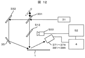
次に、図12を用いて、本発明の他の実施例である被検査物の検査装置及び被検査物の検査方法を説明する。 Next, an inspection object inspection apparatus and an inspection object inspection method according to another embodiment of the present invention will be described with reference to FIG.
本実施例の被検査物の検査装置は、図2乃至図6に示した先の実施例である被検査物の検査装置とその構成及び作用は大部分が共通しているので、両者に共通の構成については説明を省略し、相違する構成についてのみ以下に説明する。 The inspection object inspection apparatus according to the present embodiment has the same configuration and operation as the inspection object inspection apparatus according to the previous embodiment shown in FIGS. The description of this configuration is omitted, and only a different configuration will be described below.
図12において、本実施例の被検査物の検査装置では、ウェーハ1の表面におけるベベル102に該当する所定領域10と平坦な平面領域との間の境界位置Epの判別を行うために、ウェーハ1の表面に照射したレーザービーム204のレーザースポット201の形状及びレーザースポット201の形状の周辺を写すハーフミラー512と、このハーフミラー512で反射した前記レーザースポット201の形状及びレーザースポット201の形状の周辺を撮影する観察カメラ500とを設置する。観察カメラ500で撮影した前記レーザースポット201の形状の画像データ及びレーザースポット201の形状の周辺の画像データに基づき、データ処理装置52における画像認識技術によって、前記ベベルの境界位置Epの判別及び所定領域10の範囲の判別を行うようにしたものである。
In FIG. 12, in the inspection apparatus for an object to be inspected according to the present embodiment, in order to determine the boundary position Ep between the
即ち、前記被検査物であるウェーハ1の表面の上部から被検査物の表面に向かって垂直方向に前記レーザービーム204を照射する光路にハーフミラー512を配置する。さらに、このハーフミラー512を透過したレーザービーム204のレーザースポット201がウェーハ1の表面に照射されるレーザースポット201の形状の画像及びレーザースポット201の形状の周辺の画像について、前記ハーフミラー512を介して反射した前記のレーザースポット201の形状の画像及びレーザースポット201の形状の周辺の画像を撮影する観察カメラ500を備えるものである。
That is, the
つまり、投光光学系におけるレーザー光源31から出力されたレーザービーム204をミラー331によって反射させてウェーハ1の表面に向かって鉛直方向下方に垂直投射させるレーザービーム204と、ウェーハ1の表面に照射されたレーザービーム204のレーザースポット201の位置を写す画像とが干渉しないようにするために、レーザービーム204は透過させ、且つウェーハ1の表面に照射されるレーザースポット201の位置及びその周辺の画像は観察カメラ500の配置方向に反射させて撮影させるハーフミラー512を備えるものである。
That is, the
この観察カメラ500は、投光光学系が照射するレーザービーム204のレーザースポット201がウェーハ1の表面に照射されたレーザースポット201の形状、並びにこのレーザースポット201の周辺部の画像を撮像できる画素数と解像度を有する。
The
本実施例では、レーザービーム204のレーザースポット201をウェーハ1の表面に照射して走査(スキャン)中に前記したウェーハ1の表面に照射されたレーザースポット201の形状、並びにこのレーザースポット201の周辺部の画像を観察カメラ500によって撮影し、逐次、画像データとして取得して、本実施例の検査装置に備えられたデータ処理装置52で画像認識技術によって前記画像データを解析してウェーハ1の表面の前記平面領域と所定領域との間のベベルの境界位置Ep、並びにウェーハ1のベベル102に該当する前記所定領域10の範囲を判別するものである。
In the present embodiment, the surface of the
即ち、観察カメラ500によって撮影される前記レーザービーム204のレーザースポット201の形状は、例えばこのレーザースポット201が照射される位置がウェーハ1の表面の平面領域に在る場合には円形であった場合、このレーザースポット201の照射位置が前記平面領域からウェーハ1のエッジ部dに該当する所定領域10に変わるベベルの境界位置Epに入るとレーザースポット201の形状が前記べベル102の傾斜した面によって楕円形に変化する。
That is, the shape of the
このため、前記データ処理装置52にて観察カメラ500によって撮影されたレーザースポット201の形状をパターンマッチングさせる画像認識技術を適用すれば、ウェーハ1の表面の前記平面領域と所定領域10との間のベベルの境界位置Epを高精度に判別することができる。
For this reason, if an image recognition technique for pattern-matching the shape of the
また、上記と同様の手法によってウェーハ1のエッジ部dに該当する所定領域10の範囲も判別することができる。
Further, the range of the
また、ウェーハ1の表面に存在する異物eや、スクラッチ傷や結晶欠陥(COP)等の欠陥で散乱した散乱光Seは先の実施例と同様に高角度用検出器371〜374及び低角度用検出器381〜386によって検出され、前記検出器で検出された受光信号が信号処理装置4及びデータ処理装置52に送られて演算処理され、前記異物又は欠陥25の大きさや位置がディスプレイ75等に表示されるように構成されている。
Further, the scattered light Se scattered by the foreign matter e existing on the surface of the
尚、本実施例では前記ベベルの境界位置Epの判別、並びにウェーハ1の表面に存在する異物又は欠陥25の状況の判別は、図2乃至図6を用いて説明した先の実施例と同様であるので説明を省略したが、ウェーハ1の表面の前記平面領域と所定領域10との間のベベルの境界位置Epを高精度に判別すると共に、ウェーハ1の表面に存在する異物又は欠陥25から発生する散乱光Seを検出器で効果的に検出して前記異物又は欠陥25の状況を高精度に測定することが可能となる。
In this embodiment, the determination of the boundary position Ep of the bevel and the determination of the state of the foreign matter or the defect 25 existing on the surface of the
本発明の実施例によれば、被検査物の表面をレーザービームを照射して検査する場合に、被検査物の検査対象となる平面領域の範囲をできるだけ広く設定可能にするため、この平面領域と該平面領域に隣接した被検査物のエッジ部に該当する所定領域との境界位置を正確に判別して検査する被検査物の検査装置及び被検査物の検査方法が実現できる。 According to the embodiment of the present invention, when the surface of the inspection object is inspected by irradiating the laser beam, the flat area to be inspected of the inspection object can be set as wide as possible. And an inspection object inspection apparatus and inspection object inspection method for accurately inspecting and inspecting a boundary position between a predetermined area corresponding to an edge portion of the inspection object adjacent to the planar area.
次に図13を用いて本発明の更に他の実施例である被検査物の検査装置及び被検査物の検査方法を説明する。 Next, an inspection object inspection apparatus and inspection object inspection method according to still another embodiment of the present invention will be described with reference to FIG.
図13に示した本実施例の被検査物の検査装置も、図2乃至図6に示した先の実施例である被検査物の検査装置とその構成及び作用は大部分が共通しているので、両者に共通の構成については説明を省略し、相違する構成についてのみ以下に説明する。 The inspection apparatus for inspecting objects of this embodiment shown in FIG. 13 is mostly the same in configuration and operation as the inspection apparatus for inspection objects of the previous embodiments shown in FIGS. Therefore, the description of the configuration common to both is omitted, and only the configuration that is different will be described below.
図13において、本実施例の被検査物の検査装置では、ウェーハ1の表面における平坦な平面領域とベベル102に該当する所定領域10との間の境界位置Epの判別、及び判別及び所定領域10の範囲の判別、並びにウェーハ1の表面に存在する異物又は欠陥25の状況の判別は、ウェーハ1の表面にレーザービーム204のレーザースポット201を照射してウェーハ1の表面で散乱した散乱光Seを受光するために、このウェーハ1の上方に設置されて該散乱光Seを反射させる複数個の集光ミラー613と、これら複数個の集光ミラー613で反射された散乱光Seを受光するために例えば円環状に多数のセンサを配列した構成のラインセンサ600とを設置し、前記集光ミラー613で反射させた散乱光Seを受光するラインセンサ600のセンサの位置によって、この受光したセンサの受光信号に基づいて信号処理装置4及びデータ処理装置52に送られて演算処理され、前記異物又は欠陥25の大きさや位置がディスプレイ75等に表示されるように構成されている。
In the inspection apparatus for an object to be inspected according to the present embodiment shown in FIG. And the state of the foreign matter or defect 25 existing on the surface of the
そしてこの結果、ウェーハ1の表面における平坦な平面領域とエッジ部dに該当する所定領域10との間のベベルの境界位置Epの判別、及び所定領域10の範囲の判別、並びにウェーハ1の表面に存在する異物又は欠陥25の状況の判別が実行されて、前記ベベルの境界位置Epの位置及び、前記異物又は欠陥25の大きさや位置がディスプレイ75等に表示されるように構成されている。
As a result, the bevel boundary position Ep between the flat planar region on the surface of the
本実施例で散乱光Seを受光するラインセンサ600を用いる効果としては、光電子増倍管(PMT)を用いた先の実施例の検出器と比較して、強い回折光が入射した場合でも故障しにくい点が上げられる。
The effect of using the
また本実施例のラインセンサ600においても、先の実施例の検出器によって散乱光Seを受光する場合と同様に、ウェーハ1の直径方向に発生する強い回折光202の影響を受ける、又はこの強い回折光202の影響を受けやすい領域のウェーハ1の表面から散乱した散乱光Seの受光信号V1と、ウェーハ1のベベル102の接線方向に発生する弱い回折光203の影響を受ける、又はこの弱い回折光203の影響を受けやすい領域のウェーハ1の表面から散乱した散乱光Seの受光信号V2を夫々取得する。
Also in the
そして、図2乃至図6に示された先の実施例の場合の演算処理と同様に、ラインセンサ600の複数のセンサで検出した受光信号の出力電圧V1及び受光信号の出力電圧V2の比(V1/V2)の値と、任意に設定した閾値Th1とを比較して、閾値Thを越えたウェーハ1の表面の位置を、ウェーハ1の平坦な表面領域とウェーハ1のベベル102に該当する所定領域との間の境界位置Ep正確に判断することが可能となる。
Similar to the arithmetic processing in the case of the previous embodiment shown in FIGS. 2 to 6, the ratio between the output voltage V1 of the received light signal detected by the plurality of sensors of the
また本実施例のラインセンサ600では、ウェーハ1の表面に存在する異物又は欠陥25で散乱した散乱光Seを前記した回折光の影響をあまり受けずに受光できるので、これらの異物又は欠陥25の状況を高精度に検出することが可能となる。
Further, in the
更にエッジ部に該当する所定領域10に存在する異物又は欠陥25の状況を測定する場合には、ラインセンサ600のうちノイズとなる強い回折光202の影響を受けない角度の範囲に位置するセンサの部分を選択することにより感度低下を最小限に抑えて、所定領域10に存在する異物又は欠陥25の状況の検査を可能にできる。
Further, when measuring the state of the foreign matter or the defect 25 existing in the
このようにウェーハ1の表面領域と所定領域との間のベベルの境界位置Epを正確に判別することにより、ウェーハ1の表面の平坦な平面領域を最大限に利用可能とするだけでなく、従来、測定ができなかったウェーハ1のベベル102に該当する所定領域における異物又は欠陥25の状況の管理が可能となり、ウェーハ1の致命的な欠陥の見落としがなくなる。
Thus, by accurately determining the bevel boundary position Ep between the surface area of the
よって、本実施例を適用して検査したウェーハ1から製造された半導体ICの不良を大幅に低減することが可能となる。
Therefore, it is possible to greatly reduce the defects of the semiconductor IC manufactured from the
本発明の実施例によれば、被検査物の表面をレーザービームを照射して検査する場合に、被検査物の検査対象となる平面領域の範囲をできるだけ広く設定可能にするため、この平面領域と該平面領域に隣接した被検査物のエッジ部に該当する所定領域との境界位置を正確に判別して検査する被検査物の検査装置及び被検査物の検査方法が実現できる。 According to the embodiment of the present invention, when the surface of the inspection object is inspected by irradiating the laser beam, the flat area to be inspected of the inspection object can be set as wide as possible. And an inspection object inspection apparatus and inspection object inspection method for accurately inspecting and inspecting a boundary position between a predetermined area corresponding to an edge portion of the inspection object adjacent to the planar area.
さらに、本発明の実施例によれば、被検査物を検査するための検出器の出力に基づいて、ウェーハ等の被検査物の外周近傍を複数の領域に判別して、さらに、その複数の境界を判別できるので、ウェーハ等のベベル(エッジ)領域を検知するための特別な検出器が不要であるという顕著な効果を有する。 Further, according to the embodiment of the present invention, based on the output of the detector for inspecting the inspection object, the vicinity of the outer periphery of the inspection object such as a wafer is determined as a plurality of regions, Since the boundary can be discriminated, there is a remarkable effect that a special detector for detecting a bevel (edge) region such as a wafer is unnecessary.
また、被検査物を検査するための複数の検出器の出力を用いるため、ウェーハ等のベベル(エッジ)領域を検知するための特別な検出器では検出できないエッジロールオフ領域、エッジロールオフ領域より更に内周の平坦な領域、また、これらの境界(例えば、ベベル領域とエッジロールオフ領域との境界Ep、又は、エッジロールオフ領域と更に内周の平坦な領域との境界Rpなど)を判別できるので、それぞれを検出する専用の検出器を、設けなくても良いという顕著な効果を有する。 In addition, since the outputs of a plurality of detectors for inspecting an object to be inspected are used, the edge roll-off region and the edge roll-off region that cannot be detected by a special detector for detecting a bevel (edge) region such as a wafer are used. Further, the inner peripheral flat region and the boundary thereof (for example, the boundary Ep between the bevel region and the edge roll-off region, or the boundary Rp between the edge roll-off region and the inner flat region) are discriminated. Therefore, there is a remarkable effect that it is not necessary to provide a dedicated detector for detecting each.
さらに、本発明の実施例によれば、ウェーハ等の被検査物の表面の状況を検査する被検査物の検査装置及び被検査物の検査方法に適用できる。特に、ウェーハ等の被検査物の外周近傍を複数の領域に判別して、さらに、その複数の境界を判別できる。例えば、物理的な外周端の位置のみならず、ベベル領域,エッジロールオフ領域,エッジロールオフ領域より更に内周の平坦な領域、また、これらの境界(例えば、ベベル領域とエッジロールオフ領域との境界Ep、又は、エッジロールオフ領域と更に内周の平坦な領域との境界Rpなど)を判別して、検査処理に活用できるという顕著な効果を有する。 Furthermore, according to the embodiment of the present invention, the present invention can be applied to an inspection apparatus and an inspection method for an inspection object for inspecting the surface condition of the inspection object such as a wafer. In particular, the vicinity of the outer periphery of an inspection object such as a wafer can be determined as a plurality of regions, and further, the plurality of boundaries can be determined. For example, not only the position of the physical outer edge, but also a bevel area, an edge roll-off area, an area that is further flat on the inner circumference than the edge roll-off area, and a boundary between them (for example, a bevel area and an edge roll-off area) The boundary Ep or the boundary Rp between the edge roll-off region and the inner peripheral flat region can be discriminated and used for the inspection process.
また、半導体ウェーハ,絶縁物ウェーハを、物理的な外周端の位置のみならず、ベベル領域,エッジロールオフ領域,エッジロールオフ領域より更に内周の平坦な領域、また、これらの境界についての情報及びそれらにおける異物・欠陥情報を入手できるので、半導体ウェーハ,絶縁物ウェーハの品質の向上、及びこれらを貼り合わせた貼り合わせウェーハの品質の向上に貢献できる。 In addition to the position of the physical outer peripheral edge of semiconductor wafers and insulator wafers, information on the bevel area, edge roll-off area, flat area further inside the edge roll-off area, and boundaries between these areas Since foreign matter / defect information can be obtained, the quality of the semiconductor wafer and the insulator wafer can be improved, and the quality of the bonded wafer obtained by bonding these can be improved.
本発明はウェーハ等の被検査物の表面の状況を検査する被検査物の検査装置及び被検査物の検査方法に適用でき、特にレーザー光を照射してウェーハ等の被検査物の表面を検査する被検査物の検査装置及び被検査物の検査方法に利用可能である。 The present invention can be applied to an inspection object inspection apparatus and inspection object inspection method for inspecting the surface state of an inspection object such as a wafer, and in particular, inspects the surface of an inspection object such as a wafer by irradiating a laser beam. The present invention can be used for an inspection apparatus and an inspection method for an inspection object.
1 ウェーハ
4 信号処理装置
10 所定領域
21 テーブル
22 直線移動機構
25 異物又は欠陥
31 レーザー光源
35,331,332 ミラー
51 駆動制御器
52 データ処理装置
75 ディスプレイ
102 べベル(エッジ)
201 レーザースポット
202 強い回折光
203 弱い回折光
204 レーザービーム
371〜374 高角度用検出器
381〜386 低角度用検出器
500 観察カメラ
512 ハーフミラー
600 ラインセンサ
613 集光ミラー
Se 散乱光
Ep ベベルの境界位置
Th1,Th2 閾値
Rp エッジロールオフの境界位置
DESCRIPTION OF
201
Claims (14)
前記被検査物をテーブルに載置して前記テーブルを回転させる回転駆動機構と、
前記回転駆動機構を前記被検査物の移送方向に移動させる移動機構と、
前記被検査物に照射されたレーザービームによって前記被検査物の表面から放射される光を検出する複数の検出器と、
前記複数の検出器で検出された光の検出信号に基づいて、前記被検査物の表面の平坦領域と前記被検査物外周部のベベル部に該当する境界位置を判別し、被検査物を検査するデータ処理装置と、
を備えたことを特徴とする被検査物の検査装置。 A projection optical system for irradiating a laser beam to the object to be inspected
A rotational drive mechanism for rotating the table by placing the inspection object on the table;
A moving mechanism for moving the rotation drive mechanism in the transfer direction of the inspection object;
A plurality of detectors for detecting light emitted from the surface of the inspection object by a laser beam applied to the inspection object;
Based on the detection signals of the light detected by the plurality of detectors, the boundary position corresponding to the flat area on the surface of the inspection object and the bevel portion of the outer periphery of the inspection object is determined, and the inspection object is inspected A data processing device,
A device for inspecting an object to be inspected.
前記被検査物をテーブルに載置して前記テーブルを回転させる回転駆動機構と、
前記回転駆動機構を前記被検査物の移送方向に移動させる移動機構と、
前記回転駆動機構と前記移動機構の位置座標情報を発信する駆動制御器と、
前記被検査物に照射されたレーザービームによって前記被検査物の表面から放射される光を検出する複数の検出器と、
前記複数の検出器で検出された光の検出信号に基づいて、前記被検査物外周部のベベル部に該当する境界位置を判別し、前記駆動制御器からの位置座標情報と関連付けて、前記被検査物周方向の前記境界位置を出力し、被検査物を検査するデータ処理装置と、
を備えたことを特徴とする被検査物の検査装置。 A projection optical system for irradiating a laser beam to the object to be inspected;
A rotational drive mechanism for rotating the table by placing the inspection object on the table;
A moving mechanism for moving the rotation drive mechanism in the transfer direction of the inspection object;
A drive controller for transmitting position coordinate information of the rotational drive mechanism and the moving mechanism;
A plurality of detectors for detecting light emitted from the surface of the inspection object by a laser beam applied to the inspection object;
Based on detection signals of light detected by the plurality of detectors, a boundary position corresponding to a bevel portion of the outer peripheral portion of the object to be inspected is determined, and associated with position coordinate information from the drive controller, A data processing device that outputs the boundary position in the circumferential direction of the inspection object and inspects the inspection object; and
A device for inspecting an object to be inspected.
前記被検査物をテーブルに載置して前記テーブルを回転させる回転駆動機構と、
前記回転駆動機構を前記被検査物の移送方向に移動させる移動機構と、
前記回転駆動機構と前記移動機構の位置座標情報を発信する駆動制御器と、
前記被検査物に照射されたレーザービームによって前記被検査物の表面から放射される光を検出する複数の検出器と、
前記複数の検出器で検出された光の検出信号に基づいて前記被検査物外周部のベベル部に該当する境界位置を判別して、前記駆動制御器からの位置座標情報との関連付けによって前記被検査物周方向の前記境界位置を出力し、該被検査物周方向の境界位置に基づいて、前記被検査物の略中心座標を出力し、被検査物を検査するデータ処理装置と、
を備えたことを特徴とする被検査物の検査装置。 A projection optical system for irradiating a laser beam to the object to be inspected;
A rotational drive mechanism for rotating the table by placing the inspection object on the table;
A moving mechanism for moving the rotation drive mechanism in the transfer direction of the inspection object;
A drive controller for transmitting position coordinate information of the rotational drive mechanism and the moving mechanism;
A plurality of detectors for detecting light emitted from the surface of the inspection object by a laser beam applied to the inspection object;
Based on detection signals of light detected by the plurality of detectors, a boundary position corresponding to a bevel portion of the outer peripheral portion of the object to be inspected is determined, and the object to be detected is associated with position coordinate information from the drive controller. A data processing device that outputs the boundary position in the circumferential direction of the inspection object, outputs a substantially central coordinate of the inspection object based on the boundary position in the circumferential direction of the inspection object, and inspects the inspection object;
A device for inspecting an object to be inspected.
前記境界位置の判別は、前記被検査物の表面から放射される光の回折光の指向性に基づいて判別することを特徴とする被検査物の検査装置。 In any one of Claim 1 thru | or 3,
The boundary position is determined based on directivity of diffracted light emitted from the surface of the inspection object.
前記被検査物の略中心座標に基づいて、前記被検査物から検出された異物又は欠陥の位置座標を補正することを特徴とする被検査物の検査装置。 In claim 3,
An inspection apparatus for an inspection object, wherein position coordinates of a foreign object or a defect detected from the inspection object are corrected based on a substantially center coordinate of the inspection object.
前記異物又は欠陥の位置座標補正は、複数の基準線に基づいて補正することを特徴とする被検査物の検査装置。 In claim 5,
The inspection apparatus for an inspection object, wherein the position coordinate correction of the foreign matter or the defect is corrected based on a plurality of reference lines.
前記被検査物は半導体ウェーハ又は絶縁体ウェーハであることを特徴とする被検査物の検査装置。 In any one of Claims 1 thru | or 6,
The inspection object inspection apparatus, wherein the inspection object is a semiconductor wafer or an insulator wafer.
前記被検査物に照射されたレーザービームによって前記被検査物の表面から放射される光を複数の検出器で検出し、
前記複数の検出器で検出された光の検出信号に基づいて前記被検査物の表面の平坦領域と前記被検査物外周部のベベル部に該当する境界位置を判別し、被検査物を検査することを特徴とする被検査物の検査方法。 In the inspection method of the inspection object for rotating the inspection object and irradiating the inspection object with a laser beam,
A plurality of detectors detect light emitted from the surface of the inspection object by the laser beam applied to the inspection object,
Based on detection signals of light detected by the plurality of detectors, a boundary position corresponding to a flat region on the surface of the inspection object and a bevel portion of the outer periphery of the inspection object is determined, and the inspection object is inspected. A method for inspecting an object to be inspected.
前記被検査物に照射されたレーザービームによって前記被検査物の表面から放射される光を複数の検出器で検出し、
前記複数の検出器で検出された光の検出信号に基づいて前記被検査物の表面の平坦領域と前記被検査物外周部のベベル部に該当する境界位置を前記テーブルの座標情報と関連付けて判別し、
前記被検査物の境界位置分布を出力し、被検査物を検査することを特徴とする被検査物の検査方法。 In the inspection method of the inspection object that rotates the inspection object and irradiates the skin inspection object with a laser beam,
A plurality of detectors detect light emitted from the surface of the inspection object by the laser beam applied to the inspection object,
Based on detection signals of light detected by the plurality of detectors, a boundary position corresponding to a flat area on the surface of the object to be inspected and a bevel part of the outer periphery of the object to be inspected is determined in association with the coordinate information of the table. And
A method for inspecting an inspection object, wherein the inspection object is inspected by outputting a boundary position distribution of the inspection object.
前記被検査物に照射されたレーザービームによって前記被検査物の表面から放射される光を複数の検出器で検出し、
前記複数の検出器で検出された光の検出信号に基づいて前記被検査物の表面の平坦領域と前記被検査物外周部のベベル部に該当する境界位置を前記テーブルの座標情報と関連付けて判別して前記被検査物の境界位置分布を出力し、
この境界位置分布に基づいて前記被検査物の略中心座標を出力し、被検査物を検査することを特徴とする被検査物の検査方法。 In the inspection method of the inspection object in which the inspection object is inspected by rotating the table on which the inspection object is placed and irradiating the inspection object with a laser beam.
A plurality of detectors detect light emitted from the surface of the inspection object by the laser beam applied to the inspection object,
Based on detection signals of light detected by the plurality of detectors, a boundary position corresponding to a flat area on the surface of the object to be inspected and a bevel part of the outer periphery of the object to be inspected is determined in association with the coordinate information of the table. And output the boundary position distribution of the inspection object,
An inspection method for an inspection object, comprising: outputting substantially center coordinates of the inspection object based on the boundary position distribution and inspecting the inspection object.
前記被検査物は半導体ウェーハ又は絶縁体ウェーハであることを特徴とする被検査物の検査方法。 In any one of Claims 8 to 10,
The inspection object inspection method, wherein the inspection object is a semiconductor wafer or an insulator wafer.
ウェーハに照射されたレーザービームによってウェーハの表面から放射される光を複数の検出器で検出し、
前記複数の検出器で検出された光の検出信号に基づいて、ウェーハの表面の平坦領域とウェーハ外周部のエッジロールオフ領域とベベル領域とを判別することを特徴とする被検査物の検査装置。 An inspection apparatus for an object to be inspected by rotating a wafer and irradiating the wafer with a laser beam,
The light emitted from the wafer surface by the laser beam applied to the wafer is detected by multiple detectors.
An inspection apparatus for an object to be inspected, which discriminates a flat area on the surface of a wafer, an edge roll-off area and a bevel area on the outer periphery of the wafer based on detection signals of light detected by the plurality of detectors. .
ウェーハに照射されたレーザービームによってウェーハの表面から放射される光を複数の検出器で検出し、
前記複数の検出器で検出された光の検出信号に基づいて、
ウェーハの表面の平坦領域とウェーハ外周部のエッジロールオフ領域との境界位置情報、及び前記エッジロールオフ領域とベベル領域との境界位置情報を得ることを特徴とする被検査物の検査装置。 An inspection apparatus for an object to be inspected by rotating a wafer and irradiating the wafer with a laser beam,
The light emitted from the wafer surface by the laser beam applied to the wafer is detected by multiple detectors.
Based on detection signals of light detected by the plurality of detectors,
An inspection apparatus for an object to be inspected, which obtains boundary position information between a flat area on the surface of a wafer and an edge roll-off area at the outer periphery of the wafer, and boundary position information between the edge roll-off area and the bevel area.
ウェーハの表面の平坦領域とウェーハ外周部のエッジロールオフ領域との境界情報と、
前記エッジロールオフ領域とベベル領域との境界情報と、
ウェーハのノッチの座標とに基づいて、
ウェーハの偏心の状態を検出することを特徴とする被検査物の検査装置。 In claim 13,
Boundary information between the flat area of the wafer surface and the edge roll-off area of the outer periphery of the wafer,
Boundary information between the edge roll-off area and the bevel area;
Based on the coordinates of the notch of the wafer and
An inspection apparatus for an inspection object, characterized by detecting an eccentric state of a wafer.
Priority Applications (1)
| Application Number | Priority Date | Filing Date | Title |
|---|---|---|---|
| JP2008165210A JP5222635B2 (en) | 2008-06-25 | 2008-06-25 | Inspection device and inspection method for inspection object |
Applications Claiming Priority (1)
| Application Number | Priority Date | Filing Date | Title |
|---|---|---|---|
| JP2008165210A JP5222635B2 (en) | 2008-06-25 | 2008-06-25 | Inspection device and inspection method for inspection object |
Related Child Applications (1)
| Application Number | Title | Priority Date | Filing Date |
|---|---|---|---|
| JP2011041105A Division JP5427808B2 (en) | 2011-02-28 | 2011-02-28 | Inspection device |
Publications (2)
| Publication Number | Publication Date |
|---|---|
| JP2010010234A true JP2010010234A (en) | 2010-01-14 |
| JP5222635B2 JP5222635B2 (en) | 2013-06-26 |
Family
ID=41590404
Family Applications (1)
| Application Number | Title | Priority Date | Filing Date |
|---|---|---|---|
| JP2008165210A Expired - Fee Related JP5222635B2 (en) | 2008-06-25 | 2008-06-25 | Inspection device and inspection method for inspection object |
Country Status (1)
| Country | Link |
|---|---|
| JP (1) | JP5222635B2 (en) |
Cited By (2)
| Publication number | Priority date | Publication date | Assignee | Title |
|---|---|---|---|---|
| JP2011109142A (en) * | 2011-02-28 | 2011-06-02 | Hitachi High-Technologies Corp | Display device, and inspection device |
| JP2013541011A (en) * | 2010-10-12 | 2013-11-07 | ケーエルエー−テンカー コーポレイション | Coordinate fusion and thickness calibration for semiconductor wafer edge inspection |
Citations (5)
| Publication number | Priority date | Publication date | Assignee | Title |
|---|---|---|---|---|
| JPH06302676A (en) * | 1993-04-14 | 1994-10-28 | Hitachi Electron Eng Co Ltd | Wafer foreign matter inspecting apparatus |
| WO2006112466A1 (en) * | 2005-04-19 | 2006-10-26 | Matsushita Electric Industrial Co., Ltd. | Method for inspecting a foreign matter on mirror-finished substrate |
| JP2007205864A (en) * | 2006-02-01 | 2007-08-16 | Reitetsukusu:Kk | Substrate inspecting apparatus and substrate inspecting method |
| JP2008014848A (en) * | 2006-07-07 | 2008-01-24 | Hitachi High-Technologies Corp | Surface inspection method and surface inspecting device |
| JP2009222516A (en) * | 2008-03-14 | 2009-10-01 | Raytex Corp | Edge inspection apparatus and edge inspection method |
-
2008
- 2008-06-25 JP JP2008165210A patent/JP5222635B2/en not_active Expired - Fee Related
Patent Citations (5)
| Publication number | Priority date | Publication date | Assignee | Title |
|---|---|---|---|---|
| JPH06302676A (en) * | 1993-04-14 | 1994-10-28 | Hitachi Electron Eng Co Ltd | Wafer foreign matter inspecting apparatus |
| WO2006112466A1 (en) * | 2005-04-19 | 2006-10-26 | Matsushita Electric Industrial Co., Ltd. | Method for inspecting a foreign matter on mirror-finished substrate |
| JP2007205864A (en) * | 2006-02-01 | 2007-08-16 | Reitetsukusu:Kk | Substrate inspecting apparatus and substrate inspecting method |
| JP2008014848A (en) * | 2006-07-07 | 2008-01-24 | Hitachi High-Technologies Corp | Surface inspection method and surface inspecting device |
| JP2009222516A (en) * | 2008-03-14 | 2009-10-01 | Raytex Corp | Edge inspection apparatus and edge inspection method |
Cited By (2)
| Publication number | Priority date | Publication date | Assignee | Title |
|---|---|---|---|---|
| JP2013541011A (en) * | 2010-10-12 | 2013-11-07 | ケーエルエー−テンカー コーポレイション | Coordinate fusion and thickness calibration for semiconductor wafer edge inspection |
| JP2011109142A (en) * | 2011-02-28 | 2011-06-02 | Hitachi High-Technologies Corp | Display device, and inspection device |
Also Published As
| Publication number | Publication date |
|---|---|
| JP5222635B2 (en) | 2013-06-26 |
Similar Documents
| Publication | Publication Date | Title |
|---|---|---|
| JP5349742B2 (en) | Surface inspection method and surface inspection apparatus | |
| JP2008216054A (en) | Device and method for inspecting test object | |
| US8411264B2 (en) | Method and apparatus for inspecting defects | |
| US8638429B2 (en) | Defect inspecting method and defect inspecting apparatus | |
| US8482727B2 (en) | Defect inspection method | |
| US7791721B2 (en) | Surface inspection with variable digital filtering | |
| US9041921B2 (en) | Defect inspection device and defect inspection method | |
| US8949043B2 (en) | Surface inspecting apparatus and method for calibrating same | |
| JP5222635B2 (en) | Inspection device and inspection method for inspection object | |
| JP5427808B2 (en) | Inspection device | |
| US8379196B2 (en) | Method for judging whether semiconductor wafer is non-defective wafer by using laser scattering method | |
| JP5212779B2 (en) | Surface inspection apparatus and surface inspection method | |
| JP2011085602A (en) | Inspection device | |
| JP5074058B2 (en) | Foreign matter inspection method and foreign matter inspection device | |
| JP2002214155A (en) | Flaw inspecting device for test object | |
| JP6476580B2 (en) | Flat plate surface condition inspection apparatus and flat plate surface condition inspection method using the same | |
| KR101018207B1 (en) | Beam scanner and surface measurement apparatus | |
| JP2008216105A (en) | Surface inspection method and device | |
| JP2011075353A (en) | Defect inspection device and method of defect inspection |
Legal Events
| Date | Code | Title | Description |
|---|---|---|---|
| A621 | Written request for application examination |
Free format text: JAPANESE INTERMEDIATE CODE: A621 Effective date: 20110228 |
|
| A521 | Written amendment |
Free format text: JAPANESE INTERMEDIATE CODE: A523 Effective date: 20110228 |
|
| A131 | Notification of reasons for refusal |
Free format text: JAPANESE INTERMEDIATE CODE: A131 Effective date: 20121204 |
|
| A977 | Report on retrieval |
Free format text: JAPANESE INTERMEDIATE CODE: A971007 Effective date: 20121206 |
|
| A521 | Written amendment |
Free format text: JAPANESE INTERMEDIATE CODE: A523 Effective date: 20130122 |
|
| TRDD | Decision of grant or rejection written | ||
| A01 | Written decision to grant a patent or to grant a registration (utility model) |
Free format text: JAPANESE INTERMEDIATE CODE: A01 Effective date: 20130212 |
|
| A61 | First payment of annual fees (during grant procedure) |
Free format text: JAPANESE INTERMEDIATE CODE: A61 Effective date: 20130311 |
|
| FPAY | Renewal fee payment (event date is renewal date of database) |
Free format text: PAYMENT UNTIL: 20160315 Year of fee payment: 3 |
|
| R150 | Certificate of patent or registration of utility model |
Ref document number: 5222635 Country of ref document: JP Free format text: JAPANESE INTERMEDIATE CODE: R150 Free format text: JAPANESE INTERMEDIATE CODE: R150 |
|
| LAPS | Cancellation because of no payment of annual fees |