JP2010010211A - Manufacture method for semiconductor device, and semiconductor device - Google Patents
Manufacture method for semiconductor device, and semiconductor device Download PDFInfo
- Publication number
- JP2010010211A JP2010010211A JP2008164701A JP2008164701A JP2010010211A JP 2010010211 A JP2010010211 A JP 2010010211A JP 2008164701 A JP2008164701 A JP 2008164701A JP 2008164701 A JP2008164701 A JP 2008164701A JP 2010010211 A JP2010010211 A JP 2010010211A
- Authority
- JP
- Japan
- Prior art keywords
- film
- dielectric film
- electrode
- subdielectric
- annealing
- Prior art date
- Legal status (The legal status is an assumption and is not a legal conclusion. Google has not performed a legal analysis and makes no representation as to the accuracy of the status listed.)
- Granted
Links
- 239000004065 semiconductor Substances 0.000 title claims abstract description 25
- 238000004519 manufacturing process Methods 0.000 title claims abstract description 13
- 238000000034 method Methods 0.000 title claims abstract description 7
- 239000003990 capacitor Substances 0.000 claims abstract description 57
- 229910010037 TiAlN Inorganic materials 0.000 claims abstract description 42
- 239000000758 substrate Substances 0.000 claims abstract description 13
- 229910052782 aluminium Inorganic materials 0.000 claims abstract description 10
- TWNQGVIAIRXVLR-UHFFFAOYSA-N oxo(oxoalumanyloxy)alumane Chemical compound O=[Al]O[Al]=O TWNQGVIAIRXVLR-UHFFFAOYSA-N 0.000 claims abstract description 7
- BPUBBGLMJRNUCC-UHFFFAOYSA-N oxygen(2-);tantalum(5+) Chemical compound [O-2].[O-2].[O-2].[O-2].[O-2].[Ta+5].[Ta+5] BPUBBGLMJRNUCC-UHFFFAOYSA-N 0.000 claims abstract description 6
- 229910052760 oxygen Inorganic materials 0.000 claims abstract description 5
- 229910001936 tantalum oxide Inorganic materials 0.000 claims abstract description 5
- QVGXLLKOCUKJST-UHFFFAOYSA-N atomic oxygen Chemical compound [O] QVGXLLKOCUKJST-UHFFFAOYSA-N 0.000 claims abstract description 4
- 239000001301 oxygen Substances 0.000 claims abstract description 4
- XAGFODPZIPBFFR-UHFFFAOYSA-N aluminium Chemical compound [Al] XAGFODPZIPBFFR-UHFFFAOYSA-N 0.000 claims abstract description 3
- 238000000137 annealing Methods 0.000 claims description 65
- 229910018072 Al 2 O 3 Inorganic materials 0.000 description 67
- 239000010936 titanium Substances 0.000 description 23
- 239000011229 interlayer Substances 0.000 description 15
- NRTOMJZYCJJWKI-UHFFFAOYSA-N Titanium nitride Chemical compound [Ti]#N NRTOMJZYCJJWKI-UHFFFAOYSA-N 0.000 description 13
- 230000000052 comparative effect Effects 0.000 description 12
- 230000015572 biosynthetic process Effects 0.000 description 9
- 229910052719 titanium Inorganic materials 0.000 description 7
- 229910017150 AlTi Inorganic materials 0.000 description 6
- 239000000956 alloy Substances 0.000 description 6
- 229910045601 alloy Inorganic materials 0.000 description 6
- 238000005530 etching Methods 0.000 description 6
- 238000004544 sputter deposition Methods 0.000 description 6
- 238000004833 X-ray photoelectron spectroscopy Methods 0.000 description 5
- 238000011156 evaluation Methods 0.000 description 5
- 239000007789 gas Substances 0.000 description 5
- 239000000463 material Substances 0.000 description 5
- 239000000203 mixture Substances 0.000 description 5
- 238000002955 isolation Methods 0.000 description 4
- 239000012298 atmosphere Substances 0.000 description 3
- 230000007423 decrease Effects 0.000 description 3
- 238000005259 measurement Methods 0.000 description 3
- 230000003647 oxidation Effects 0.000 description 3
- 238000007254 oxidation reaction Methods 0.000 description 3
- 230000001590 oxidative effect Effects 0.000 description 3
- 238000000623 plasma-assisted chemical vapour deposition Methods 0.000 description 3
- GWEVSGVZZGPLCZ-UHFFFAOYSA-N Titan oxide Chemical compound O=[Ti]=O GWEVSGVZZGPLCZ-UHFFFAOYSA-N 0.000 description 2
- 239000012159 carrier gas Substances 0.000 description 2
- 230000000694 effects Effects 0.000 description 2
- 229910052751 metal Inorganic materials 0.000 description 2
- 239000002184 metal Substances 0.000 description 2
- 229910052757 nitrogen Inorganic materials 0.000 description 2
- 238000004151 rapid thermal annealing Methods 0.000 description 2
- 239000002994 raw material Substances 0.000 description 2
- 238000005546 reactive sputtering Methods 0.000 description 2
- OGIDPMRJRNCKJF-UHFFFAOYSA-N titanium oxide Inorganic materials [Ti]=O OGIDPMRJRNCKJF-UHFFFAOYSA-N 0.000 description 2
- JLTRXTDYQLMHGR-UHFFFAOYSA-N trimethylaluminium Chemical compound C[Al](C)C JLTRXTDYQLMHGR-UHFFFAOYSA-N 0.000 description 2
- WFKWXMTUELFFGS-UHFFFAOYSA-N tungsten Chemical compound [W] WFKWXMTUELFFGS-UHFFFAOYSA-N 0.000 description 2
- 229910052721 tungsten Inorganic materials 0.000 description 2
- 239000010937 tungsten Substances 0.000 description 2
- PNEYBMLMFCGWSK-UHFFFAOYSA-N aluminium oxide Inorganic materials [O-2].[O-2].[O-2].[Al+3].[Al+3] PNEYBMLMFCGWSK-UHFFFAOYSA-N 0.000 description 1
- 230000015556 catabolic process Effects 0.000 description 1
- 238000000151 deposition Methods 0.000 description 1
- 230000008021 deposition Effects 0.000 description 1
- 238000001514 detection method Methods 0.000 description 1
- 238000010438 heat treatment Methods 0.000 description 1
- 238000009616 inductively coupled plasma Methods 0.000 description 1
- 239000012212 insulator Substances 0.000 description 1
- 239000010410 layer Substances 0.000 description 1
- 238000012986 modification Methods 0.000 description 1
- 230000004048 modification Effects 0.000 description 1
- 239000012299 nitrogen atmosphere Substances 0.000 description 1
- 238000007788 roughening Methods 0.000 description 1
- 229910052710 silicon Inorganic materials 0.000 description 1
- 239000010703 silicon Substances 0.000 description 1
- 229910052814 silicon oxide Inorganic materials 0.000 description 1
- 238000001228 spectrum Methods 0.000 description 1
- 239000002344 surface layer Substances 0.000 description 1
- 230000003746 surface roughness Effects 0.000 description 1
- HSXKFDGTKKAEHL-UHFFFAOYSA-N tantalum(v) ethoxide Chemical compound [Ta+5].CC[O-].CC[O-].CC[O-].CC[O-].CC[O-] HSXKFDGTKKAEHL-UHFFFAOYSA-N 0.000 description 1
- 238000012795 verification Methods 0.000 description 1
Images


Classifications
-
- H—ELECTRICITY
- H01—ELECTRIC ELEMENTS
- H01L—SEMICONDUCTOR DEVICES NOT COVERED BY CLASS H10
- H01L21/00—Processes or apparatus adapted for the manufacture or treatment of semiconductor or solid state devices or of parts thereof
- H01L21/70—Manufacture or treatment of devices consisting of a plurality of solid state components formed in or on a common substrate or of parts thereof; Manufacture of integrated circuit devices or of parts thereof
- H01L21/71—Manufacture of specific parts of devices defined in group H01L21/70
- H01L21/768—Applying interconnections to be used for carrying current between separate components within a device comprising conductors and dielectrics
- H01L21/76838—Applying interconnections to be used for carrying current between separate components within a device comprising conductors and dielectrics characterised by the formation and the after-treatment of the conductors
- H01L21/76841—Barrier, adhesion or liner layers
- H01L21/7687—Thin films associated with contacts of capacitors
-
- C—CHEMISTRY; METALLURGY
- C23—COATING METALLIC MATERIAL; COATING MATERIAL WITH METALLIC MATERIAL; CHEMICAL SURFACE TREATMENT; DIFFUSION TREATMENT OF METALLIC MATERIAL; COATING BY VACUUM EVAPORATION, BY SPUTTERING, BY ION IMPLANTATION OR BY CHEMICAL VAPOUR DEPOSITION, IN GENERAL; INHIBITING CORROSION OF METALLIC MATERIAL OR INCRUSTATION IN GENERAL
- C23C—COATING METALLIC MATERIAL; COATING MATERIAL WITH METALLIC MATERIAL; SURFACE TREATMENT OF METALLIC MATERIAL BY DIFFUSION INTO THE SURFACE, BY CHEMICAL CONVERSION OR SUBSTITUTION; COATING BY VACUUM EVAPORATION, BY SPUTTERING, BY ION IMPLANTATION OR BY CHEMICAL VAPOUR DEPOSITION, IN GENERAL
- C23C14/00—Coating by vacuum evaporation, by sputtering or by ion implantation of the coating forming material
- C23C14/06—Coating by vacuum evaporation, by sputtering or by ion implantation of the coating forming material characterised by the coating material
- C23C14/0641—Nitrides
-
- C—CHEMISTRY; METALLURGY
- C23—COATING METALLIC MATERIAL; COATING MATERIAL WITH METALLIC MATERIAL; CHEMICAL SURFACE TREATMENT; DIFFUSION TREATMENT OF METALLIC MATERIAL; COATING BY VACUUM EVAPORATION, BY SPUTTERING, BY ION IMPLANTATION OR BY CHEMICAL VAPOUR DEPOSITION, IN GENERAL; INHIBITING CORROSION OF METALLIC MATERIAL OR INCRUSTATION IN GENERAL
- C23C—COATING METALLIC MATERIAL; COATING MATERIAL WITH METALLIC MATERIAL; SURFACE TREATMENT OF METALLIC MATERIAL BY DIFFUSION INTO THE SURFACE, BY CHEMICAL CONVERSION OR SUBSTITUTION; COATING BY VACUUM EVAPORATION, BY SPUTTERING, BY ION IMPLANTATION OR BY CHEMICAL VAPOUR DEPOSITION, IN GENERAL
- C23C16/00—Chemical coating by decomposition of gaseous compounds, without leaving reaction products of surface material in the coating, i.e. chemical vapour deposition [CVD] processes
- C23C16/22—Chemical coating by decomposition of gaseous compounds, without leaving reaction products of surface material in the coating, i.e. chemical vapour deposition [CVD] processes characterised by the deposition of inorganic material, other than metallic material
- C23C16/30—Deposition of compounds, mixtures or solid solutions, e.g. borides, carbides, nitrides
- C23C16/40—Oxides
- C23C16/403—Oxides of aluminium, magnesium or beryllium
-
- C—CHEMISTRY; METALLURGY
- C23—COATING METALLIC MATERIAL; COATING MATERIAL WITH METALLIC MATERIAL; CHEMICAL SURFACE TREATMENT; DIFFUSION TREATMENT OF METALLIC MATERIAL; COATING BY VACUUM EVAPORATION, BY SPUTTERING, BY ION IMPLANTATION OR BY CHEMICAL VAPOUR DEPOSITION, IN GENERAL; INHIBITING CORROSION OF METALLIC MATERIAL OR INCRUSTATION IN GENERAL
- C23C—COATING METALLIC MATERIAL; COATING MATERIAL WITH METALLIC MATERIAL; SURFACE TREATMENT OF METALLIC MATERIAL BY DIFFUSION INTO THE SURFACE, BY CHEMICAL CONVERSION OR SUBSTITUTION; COATING BY VACUUM EVAPORATION, BY SPUTTERING, BY ION IMPLANTATION OR BY CHEMICAL VAPOUR DEPOSITION, IN GENERAL
- C23C16/00—Chemical coating by decomposition of gaseous compounds, without leaving reaction products of surface material in the coating, i.e. chemical vapour deposition [CVD] processes
- C23C16/22—Chemical coating by decomposition of gaseous compounds, without leaving reaction products of surface material in the coating, i.e. chemical vapour deposition [CVD] processes characterised by the deposition of inorganic material, other than metallic material
- C23C16/30—Deposition of compounds, mixtures or solid solutions, e.g. borides, carbides, nitrides
- C23C16/40—Oxides
- C23C16/405—Oxides of refractory metals or yttrium
-
- H—ELECTRICITY
- H01—ELECTRIC ELEMENTS
- H01G—CAPACITORS; CAPACITORS, RECTIFIERS, DETECTORS, SWITCHING DEVICES OR LIGHT-SENSITIVE DEVICES, OF THE ELECTROLYTIC TYPE
- H01G4/00—Fixed capacitors; Processes of their manufacture
- H01G4/002—Details
- H01G4/005—Electrodes
- H01G4/008—Selection of materials
-
- H—ELECTRICITY
- H01—ELECTRIC ELEMENTS
- H01G—CAPACITORS; CAPACITORS, RECTIFIERS, DETECTORS, SWITCHING DEVICES OR LIGHT-SENSITIVE DEVICES, OF THE ELECTROLYTIC TYPE
- H01G4/00—Fixed capacitors; Processes of their manufacture
- H01G4/33—Thin- or thick-film capacitors
-
- H—ELECTRICITY
- H01—ELECTRIC ELEMENTS
- H01L—SEMICONDUCTOR DEVICES NOT COVERED BY CLASS H10
- H01L21/00—Processes or apparatus adapted for the manufacture or treatment of semiconductor or solid state devices or of parts thereof
- H01L21/02—Manufacture or treatment of semiconductor devices or of parts thereof
- H01L21/04—Manufacture or treatment of semiconductor devices or of parts thereof the devices having at least one potential-jump barrier or surface barrier, e.g. PN junction, depletion layer or carrier concentration layer
- H01L21/18—Manufacture or treatment of semiconductor devices or of parts thereof the devices having at least one potential-jump barrier or surface barrier, e.g. PN junction, depletion layer or carrier concentration layer the devices having semiconductor bodies comprising elements of Group IV of the Periodic System or AIIIBV compounds with or without impurities, e.g. doping materials
- H01L21/28—Manufacture of electrodes on semiconductor bodies using processes or apparatus not provided for in groups H01L21/20 - H01L21/268
- H01L21/283—Deposition of conductive or insulating materials for electrodes conducting electric current
- H01L21/285—Deposition of conductive or insulating materials for electrodes conducting electric current from a gas or vapour, e.g. condensation
- H01L21/28506—Deposition of conductive or insulating materials for electrodes conducting electric current from a gas or vapour, e.g. condensation of conductive layers
- H01L21/28512—Deposition of conductive or insulating materials for electrodes conducting electric current from a gas or vapour, e.g. condensation of conductive layers on semiconductor bodies comprising elements of Group IV of the Periodic System
- H01L21/2855—Deposition of conductive or insulating materials for electrodes conducting electric current from a gas or vapour, e.g. condensation of conductive layers on semiconductor bodies comprising elements of Group IV of the Periodic System by physical means, e.g. sputtering, evaporation
-
- H—ELECTRICITY
- H01—ELECTRIC ELEMENTS
- H01L—SEMICONDUCTOR DEVICES NOT COVERED BY CLASS H10
- H01L21/00—Processes or apparatus adapted for the manufacture or treatment of semiconductor or solid state devices or of parts thereof
- H01L21/02—Manufacture or treatment of semiconductor devices or of parts thereof
- H01L21/04—Manufacture or treatment of semiconductor devices or of parts thereof the devices having at least one potential-jump barrier or surface barrier, e.g. PN junction, depletion layer or carrier concentration layer
- H01L21/18—Manufacture or treatment of semiconductor devices or of parts thereof the devices having at least one potential-jump barrier or surface barrier, e.g. PN junction, depletion layer or carrier concentration layer the devices having semiconductor bodies comprising elements of Group IV of the Periodic System or AIIIBV compounds with or without impurities, e.g. doping materials
- H01L21/28—Manufacture of electrodes on semiconductor bodies using processes or apparatus not provided for in groups H01L21/20 - H01L21/268
- H01L21/283—Deposition of conductive or insulating materials for electrodes conducting electric current
- H01L21/285—Deposition of conductive or insulating materials for electrodes conducting electric current from a gas or vapour, e.g. condensation
- H01L21/28506—Deposition of conductive or insulating materials for electrodes conducting electric current from a gas or vapour, e.g. condensation of conductive layers
- H01L21/28512—Deposition of conductive or insulating materials for electrodes conducting electric current from a gas or vapour, e.g. condensation of conductive layers on semiconductor bodies comprising elements of Group IV of the Periodic System
- H01L21/28556—Deposition of conductive or insulating materials for electrodes conducting electric current from a gas or vapour, e.g. condensation of conductive layers on semiconductor bodies comprising elements of Group IV of the Periodic System by chemical means, e.g. CVD, LPCVD, PECVD, laser CVD
-
- H—ELECTRICITY
- H01—ELECTRIC ELEMENTS
- H01L—SEMICONDUCTOR DEVICES NOT COVERED BY CLASS H10
- H01L28/00—Passive two-terminal components without a potential-jump or surface barrier for integrated circuits; Details thereof; Multistep manufacturing processes therefor
- H01L28/40—Capacitors
Abstract
Description
本発明は、MIM(Metal Insulator Metal)キャパシタを含む半導体装置の製造方法、及びMIMキャパシタを含む半導体装置に関する。 The present invention relates to a method for manufacturing a semiconductor device including an MIM (Metal Insulator Metal) capacitor and a semiconductor device including an MIM capacitor.
アナログ素子及び高周波素子等に用いられるMIMキャパシタは、素子の高集積化に伴い微細化が進んでいる。微細化に伴うキャパシタンスの低下を補償するために、誘電体膜をより薄くする必要がある。ところが、誘電体膜を薄くすることは、リーク電流の増大につながる。このため、誘電体膜の薄膜化には限界がある。 MIM capacitors used for analog elements, high-frequency elements, and the like are increasingly miniaturized as the elements are highly integrated. In order to compensate for a decrease in capacitance due to miniaturization, it is necessary to make the dielectric film thinner. However, reducing the dielectric film leads to an increase in leakage current. For this reason, there is a limit to thinning the dielectric film.
リーク電流の増大を生じさせることなく、かつ大きなキャパシタンスを維持するために、誘電体膜に、従来のSiON等に比べて誘電率の高い高誘電率材料が採用されつつある。高誘電率材料の例として、アルミナ(Al2O3)、酸化タンタル(Ta2O5)等が挙げられる。また、MIMキャパシタの下部電極には、一般的に窒化チタン(TiN)が用いられる。 In order to maintain a large capacitance without causing an increase in leakage current, a high dielectric constant material having a dielectric constant higher than that of conventional SiON or the like is being adopted for the dielectric film. Examples of the high dielectric constant material include alumina (Al 2 O 3 ) and tantalum oxide (Ta 2 O 5 ). Further, titanium nitride (TiN) is generally used for the lower electrode of the MIM capacitor.
下部電極を構成するTiNが、誘電体膜の成膜時の酸化性雰囲気に晒されると、下部電極の表面が酸化されて酸化チタンが形成される。下部電極の表面に形成された酸化チタンは、リーク電流増大や歩留まり低下の要因になる。TiN膜の上にAlN膜を形成し、その上に酸化物誘電体膜を形成することにより、TiN膜の酸化を防止することができる(特許文献1)。 When TiN constituting the lower electrode is exposed to an oxidizing atmosphere when forming the dielectric film, the surface of the lower electrode is oxidized to form titanium oxide. Titanium oxide formed on the surface of the lower electrode causes an increase in leakage current and a decrease in yield. By forming an AlN film on the TiN film and forming an oxide dielectric film thereon, oxidation of the TiN film can be prevented (Patent Document 1).
Alの下部電極上に、Ta2O5膜を形成し、熱処理を行うことにより、両者の界面にAl2O3膜を形成することができる。Al2O3膜を形成することにより、耐圧を高めることができる(特許文献2)。 By forming a Ta 2 O 5 film on the Al lower electrode and performing heat treatment, an Al 2 O 3 film can be formed at the interface between the two . By forming the Al 2 O 3 film, the breakdown voltage can be increased (Patent Document 2).
次世代デバイスでは、リーク電流の増大を招くことなく、かつ単位面積当たりのキャパシタ容量をより大きくする技術が求められている。従来の構造では、次世代デバイスに求められるリーク電流及びキャパシタ容量を実現することが困難である。 In the next-generation device, there is a demand for a technique for increasing the capacitor capacity per unit area without increasing the leakage current. In the conventional structure, it is difficult to realize a leakage current and a capacitor capacity required for the next generation device.
上記課題を解決する半導体装置の製造方法は、
半導体基板の上に、TiAlNを含む第1の電極膜と、酸化タンタルを含む主誘電体膜とを形成する工程と、
前記第1の電極膜と前記主誘電体膜とが形成されている状態でアニールを行うことにより、前記第1の電極膜中のアルミニウム(Al)と前記主誘電体膜中の酸素(O)とを反応させて、前記第1の電極膜と前記主誘電体膜との界面に、酸化アルミニウムを含む副誘電体膜を形成する工程と、
前記主誘電体膜と前記副誘電体膜とを介して前記第1の電極膜に対向する位置に第2の電極膜を形成する工程と
を有する。
A method of manufacturing a semiconductor device that solves the above problems is as follows.
Forming a first electrode film containing TiAlN and a main dielectric film containing tantalum oxide on a semiconductor substrate;
By performing annealing in a state where the first electrode film and the main dielectric film are formed, aluminum (Al) in the first electrode film and oxygen (O) in the main dielectric film are formed. And forming a sub-dielectric film containing aluminum oxide at the interface between the first electrode film and the main dielectric film;
Forming a second electrode film at a position facing the first electrode film via the main dielectric film and the sub-dielectric film.
この製造方法により作製される半導体装置は、
半導体基板の上に配置され、TiAlNを含む第1の電極、酸化アルミニウムを含む副誘電体膜、酸化タンタルを含む主誘電体膜、及び第2の電極が、この順番にまたは逆の順番に積層され、該第1の電極と副誘電体膜とが相互に接し、該副誘電体膜と主誘電体膜とが相互に接するキャパシタを有する。
The semiconductor device manufactured by this manufacturing method is
A first electrode including TiAlN, a sub-dielectric film including aluminum oxide, a main dielectric film including tantalum oxide, and a second electrode disposed on a semiconductor substrate are stacked in this order or in reverse order. The first electrode and the sub dielectric film are in contact with each other, and the sub dielectric film and the main dielectric film have a capacitor in contact with each other.
アニールで、副誘電体膜を形成することにより、CVD等で形成する場合に比べて、薄くても全面を連続的に覆う膜が得られる。このため、リーク電流の増大を抑制することができる。 By forming the sub-dielectric film by annealing, a film that continuously covers the entire surface can be obtained even if it is thin as compared with the case where it is formed by CVD or the like. For this reason, an increase in leakage current can be suppressed.
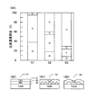
図1A〜図1Fを参照して、実施例による半導体装置の製造方法について説明する。図1A〜図1Fは、製造途中段階における主要部の断面図を示す。 With reference to FIG. 1A to FIG. 1F, a method of manufacturing a semiconductor device according to an embodiment will be described. 1A to 1F are cross-sectional views of main parts in the middle of manufacturing.
図1Aに示すように、シリコン等の半導体基板10の表層部に、シャロートレンチアイソレーション(STI)等による素子分離絶縁膜11を形成する。半導体基板10には、直径300mmのウエハを用いた。素子分離絶縁膜11で囲まれた活性領域に、MISFET12を形成する。MISFET12を覆うように、半導体基板10の上に、層間絶縁膜15を形成する。層間絶縁膜15にビアホールを形成し、ビアホール内にタングステン等の導電プラグ16を充填する。導電プラグ16は、例えばMISFET12のソースに接続される。
As shown in FIG. 1A, an element
層間絶縁膜16の上に2層目の層間絶縁膜17を形成する。層間絶縁膜17内に、例えばシングルダマシン法により配線18を形成する。配線18は、導電プラグ16に接続される。層間絶縁膜17の上に、3層目の層間絶縁膜19を形成する。層間絶縁膜19にビアホールを形成し、このビアホール内にタングステン等の導電プラグ20を充填する。導電プラグ20は、配線18に接続される。
A second
層間絶縁膜19の上に、TiAlNからなる下部電極膜30を形成する。下部電極膜30は、例えばDCマグネトロン反応性スパッタリングにより形成される。成膜条件は、例えば下記の通りである。
・ターゲット AlTi合金
・基板温度 300℃
・スパッタガス Ar(流量500sccm)+N2(流量25sccm)
・DC印加パワー 1kW
・圧力 40Pa(0.3Torr)
下部電極膜30の上に、Ta2O5からなる主誘電体膜31を形成する。主誘電体膜31は、例えばプラズマ励起化学気相成長(PE−CVD)により形成される。成膜条件は、例えば下記の通りである。
・Ta原料 ペンタエトキシタンタル(Ta(OEt)5)
・酸化ガス O2(流量100sccm)
・キャリアガス Ar(流量500sccm)
・基板温度 300℃
・RFパワー 450W
・圧力 1.3×10³Pa(10Torr)
主誘電体膜31の上に、Al2O3からなる上部副誘電体膜32を形成する。上部副誘電体膜32は、例えばPE−CVDにより形成される。成膜条件は、例えば下記の通りである。
・Al原料 トリメチルアルミニウム(TMA)
・酸化ガス O2(流量150sccm)
・キャリアガス Ar(流量500sccm)
・基板温度 300℃
・RFパワー 600W
・圧力 1.3×10³Pa(10Torr)
図1Bに示すように、N2またはAr雰囲気において、アニールを行う。このアニールには、例えばラピッドサーマルアニール(RTA)が用いられる。アニール条件は、例えば下記の通りである。
・圧力 1.0×10⁵Pa(760Torr)
・N2またはAr流量 3slm
・アニール時間 1分
・アニール温度 400℃〜600℃
このアニールにより、下部電極膜30内のAlと、主誘電体膜31内のOとが反応し、両者の界面にAl2O3からなる下部副誘電体膜35が形成される。下部副誘電体膜35が形成されていることは、X線光電子分光分析(XPS)により確認した。XPSの結果については、後に図2A〜図2Cを参照して説明する。
A
・ Target AlTi alloy ・ Substrate
・ Sputtering gas Ar (
・ DC applied power 1kW
・ Pressure 40Pa (0.3 Torr)
A main
・ Ta raw material Pentaethoxytantalum (Ta (OEt) 5 )
・ Oxidizing gas O 2 (
・ Carrier gas Ar (flow rate 500sccm)
・
・ RF power 450W
・ Pressure 1.3 × 10 3 Pa (10 Torr)
An upper
・ Al raw material Trimethylaluminum (TMA)
・ Oxidizing gas O 2 (flow rate 150 sccm)
・ Carrier gas Ar (flow rate 500sccm)
・
・ RF power 600W
・ Pressure 1.3 × 10 3 Pa (10 Torr)
As shown in FIG. 1B, annealing is performed in an N 2 or Ar atmosphere. For this annealing, for example, rapid thermal annealing (RTA) is used. Annealing conditions are, for example, as follows.
・ Pressure 1.0 × 10 5 Pa (760 Torr)
・ N 2 or
・
By this annealing, Al in the
図1Cに示すように、上部副誘電体膜32の上に、TiNからなる上部電極膜38を形成する。上部電極膜38は、例えばDCマグネトロン反応性スパッタリングにより形成される。成膜条件は、例えば下記の通りである。
・ターゲット Ti
・スパッタガス Ar(流量500sccm)+N2(流量500sccm)
・DC印加パワー 1kW
・圧力 67Pa(0.5Torr)
・成膜時間 3分
図1Dに示すように、上部電極膜38から下部電極膜30までの各膜を同一のエッチングマスクを用いてパターニングする。これらの膜のエッチングは、例えば2周波誘導結合型プラズマエッチング装置を用いて行う。エッチング条件は、例えば下記の通りである。
・エッチングガス CHF3(流量30sccm)+Ar(流量100sccm)
・圧力 2.0Pa(15mTorr)
・エッチング時間 44秒
・RFパワー 100W/500W
TiAlNからなる下部電極30a、Al2O3からなる下部副誘電体膜35a、Ta2O5からなる主誘電体膜31a、Al2O3からなる上部副誘電体膜32a、及びTiNからなる上部電極38aにより、MIMキャパシタ40が構成される。平面視において、MIMキャパシタ40は、その下の導電プラグ20を内包する。
As shown in FIG. 1C, an
・ Target Ti
Sputtering gas Ar (flow
・ DC applied power 1kW
・ Pressure 67Pa (0.5 Torr)
-
Etching gas CHF 3 (flow
・ Pressure 2.0Pa (15mTorr)
・ Etching time 44 seconds ・ RF power 100W / 500W
図1Eに示すように、層間絶縁膜19の上にさらに層間絶縁膜45を形成する。層間絶縁膜45はMIMキャパシタ40を被覆する。
As shown in FIG. 1E, an
図1Fに示すように、層間絶縁膜45にビアホールを形成し、このビアホール内に導電プラグ46を充填する。導電プラグ46は、平面視においてMIMキャパシタ40に内包され、上部電極38aに接続される。上部電極38aは、接地線または電源線に接続される。
As shown in FIG. 1F, a via hole is formed in the
図2A〜図2Cを参照して、TiAlN下部電極膜30とTa2O5主誘電体膜31との界面に、アニールによってAl2O3下部副誘電体膜35が形成されることの検証結果について説明する。
2A to 2C, the verification result that the Al 2 O 3
図2Bに、作製した試料のアニール前の断面図を示す。基板上に厚さ5nmのTiAlN下部電極膜30が形成され、その上に厚さ5nmのTa2O5主誘電体膜31が形成されている。下部電極膜30の成膜には、Tiに対するAlの含有量の比Al/Ti=30原子%のAlTi合金ターゲットを用いた。アニールは、N2雰囲気中で400℃で行った。
FIG. 2B shows a cross-sectional view of the manufactured sample before annealing. A TiAlN
アニール前、及びアニール後の試料について、XPSでAlの2p3/2スペクトルを観察した。TiAlNに起因するピークは73.9eVの位置に現れ、Al2O3に起因するピークは74.1eVの位置に現れる。 About the sample before annealing and the sample after annealing, the 2p3 / 2 spectrum of Al was observed by XPS. A peak attributed to TiAlN appears at a position of 73.9 eV, and a peak attributed to Al 2 O 3 appears at a position of 74.1 eV.
図2Aに、TiAlNに起因するピークと、Al2O3に起因するピークとの高さの割合を算出した結果を示す。アニール前では、Al2O3に起因するピークは観察されなかったが、アニール後は、Al2O3に起因するピークが観察された。この評価結果から、アニール前には、図2Bに示すように、Al2O3膜は形成されていないが、アニール後の試料では、図2Cに示すように、TiAlN下部電極膜30とTa2O5主誘電体膜31との界面にAl2O3下部副誘電体膜35が形成されていることがわかる。アニール後の試料において、TiAlNに起因するピークが観察されるのは、Al2O3下部副誘電体膜35が薄いため、その下のTiAlNが検知されるためである。下部副誘電体膜35の厚さは0.53nmであった。
FIG. 2A shows the result of calculating the height ratio between the peak due to TiAlN and the peak due to Al 2 O 3 . Prior to annealing, no peak attributed to Al 2 O 3 was observed, but after annealing, a peak attributed to Al 2 O 3 was observed. From this evaluation result, an Al 2 O 3 film was not formed before annealing as shown in FIG. 2B. However, in the sample after annealing, as shown in FIG. 2C, the TiAlN
上記実施例によるMIMキャパシタ及び従来のMIMキャパシタ(比較例)を作製し、単位面積当たりのキャパシタ容量及びリーク電流を測定した。 The MIM capacitor according to the above example and the conventional MIM capacitor (comparative example) were manufactured, and the capacitor capacity and leakage current per unit area were measured.
図3Aに、実施例によるMIMキャパシタの断面図を示し、図3Bに、比較例によるMIMキャパシタの断面図を示す。実施例によるMIMキャパシタのAl2O3下部副誘電体膜35は、アニールによって形成される。比較例のMIMキャパシタは、下部電極となるTiN膜、AlN膜、Al2O3膜、Ta2O5膜、Al2O3膜、AlN膜、及び上部電極となるTiN膜の7層で構成される。比較例のMIMキャパシタの上下のAl2O3膜は、いずれもCVDで形成される。
FIG. 3A shows a cross-sectional view of the MIM capacitor according to the embodiment, and FIG. 3B shows a cross-sectional view of the MIM capacitor according to the comparative example. The Al 2 O 3
実施例の試料では、Ta2O5主誘電体膜31の厚さを6nmとし、Al2O3上部副誘電体膜32の厚さを4nmとした。比較例の試料では、下部AlN膜、Ta2O5膜、上部Al2O3膜、及び上部AlN膜の厚さを、それぞれ50nm、6nm、4nm、及び50nmとした。
In the sample of the example, the thickness of the Ta 2 O 5 main
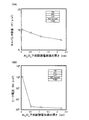
図3Cに、実施例及び比較例によるMIMキャパシタの単位面積当たりのキャパシタ容量と、Al2O3下部副誘電体膜の厚さとの関係を示す。横軸は、下部副誘電体膜の厚さを単位「nm」で表し、縦軸は、キャパシタ容量を単位「fF/μm2」で表す。黒丸記号及び白四角記号が、それぞれ実施例及び比較例のMIMキャパシタの測定結果を示す。下部副誘電体膜が厚くなるに従って、キャパシタ容量が低下している。実施例及び比較例において、キャパシタ容量がほぼ等しくなるように、各誘電体膜の厚さが設定されている。 FIG. 3C shows the relationship between the capacitor capacity per unit area of the MIM capacitor according to the example and the comparative example and the thickness of the Al 2 O 3 lower subdielectric film. The horizontal axis represents the thickness of the lower subdielectric film in the unit “nm”, and the vertical axis represents the capacitor capacity in the unit “fF / μm 2 ”. A black circle symbol and a white square symbol indicate the measurement results of the MIM capacitors of the example and the comparative example, respectively. As the lower subdielectric film becomes thicker, the capacitor capacity decreases. In the example and the comparative example, the thickness of each dielectric film is set so that the capacitor capacitances are substantially equal.
図3Dに、実施例によるMIMキャパシタの単位面積当たりのリーク電流と、下部副誘電体膜の厚さとの関係を示す。横軸は、下部副誘電体膜の厚さを単位「nm」で表し、縦軸は、リーク電流を単位「fA/μm2」で表す。リーク電流は、MIMキャパシタの電極間に3Vの直流電圧を印加して測定した。黒丸記号及び白四角記号が、それぞれ実施例及び比較例のMIMキャパシタの測定結果を示す。 FIG. 3D shows the relationship between the leakage current per unit area of the MIM capacitor according to the example and the thickness of the lower subdielectric film. The horizontal axis represents the thickness of the lower subdielectric film in the unit “nm”, and the vertical axis represents the leakage current in the unit “fA / μm 2 ”. The leakage current was measured by applying a DC voltage of 3 V between the electrodes of the MIM capacitor. A black circle symbol and a white square symbol indicate the measurement results of the MIM capacitors of the example and the comparative example, respectively.
比較例の試料では、下部副誘電体膜の厚さが1.5nm以下になると、リーク電流が急激に増加する。これに対し、実施例の試料では、下部副誘電体膜の厚さが少なくとも0.5nm〜2nmの範囲内でほぼ一定であり、下部副誘電体膜の厚さが1.5nm以下になっても、リーク電流の急激な増大は見られない。 In the sample of the comparative example, when the thickness of the lower subdielectric film becomes 1.5 nm or less, the leakage current increases rapidly. On the other hand, in the sample of the example, the thickness of the lower subdielectric film is almost constant within a range of at least 0.5 nm to 2 nm, and the thickness of the lower subdielectric film is 1.5 nm or less. However, there is no rapid increase in leakage current.
この評価結果から、下部副誘電体膜をアニールで形成することにより、CVDで形成する場合に比べて、キャパシタ容量を大きく維持したまま、リーク電流の増大を抑制できることがわかる。 From this evaluation result, it can be seen that by forming the lower subdielectric film by annealing, it is possible to suppress an increase in leakage current while maintaining a large capacitor capacity compared to the case of forming by CVD.
図4A〜図4Dを参照して、アニール、CVD、及びスパッタリングにより形成したAl2O3膜の膜質の評価結果について説明する。 With reference to FIG. 4A to FIG. 4D, the evaluation results of the film quality of the Al 2 O 3 film formed by annealing, CVD, and sputtering will be described.
図4Aに、試料S1、S2、及びS3の元素濃度割合をXPSにより測定した結果を示す。いずれの試料も、厚さ150nmのTiAlN膜の上に、厚さ2nmのAl2O3膜、及び厚さ3nmのTa2O5膜が形成されたものである。試料S1のAl2O3膜は、実施例による下部副誘電体膜35の形成と同じアニールを用いて形成した。試料S2のAl2O3膜はCVDにより形成し、試料S3のAl2O3膜はスパッタリングにより形成した。
FIG. 4A shows the result of measuring the element concentration ratio of samples S1, S2, and S3 by XPS. In each sample, an Al 2 O 3 film having a thickness of 2 nm and a Ta 2 O 5 film having a thickness of 3 nm are formed on a TiAlN film having a thickness of 150 nm. The Al 2 O 3 film of sample S1 was formed using the same annealing as the formation of the
試料S1においては、Tiが検知されず、実質的にAlとOのみが検知されている。この結果から、図4Bに示すように、TiAlN膜の全面をAl2O3膜が連続的に覆っていると考えられる。これに対し、試料S2及びS3においては、Al2O3膜の下地のTiが検知されている。この結果から、試料S2及びS3においては、図4C及び図4Dに示すように、Al2O3膜がTiAlN膜の全面を連続的に覆っておらず、Ta2O5膜がTiAlN膜に直接接触する領域が存在すると考えられる。試料S2の方が、試料S3よりも、Tiの検出割合が低い。このことから、Al2O3膜によるTiAlN膜の被覆率は、試料S2の方が試料S3よりも高いと考えられる。 In the sample S1, Ti is not detected, but only Al and O are substantially detected. From this result, it is considered that the Al 2 O 3 film continuously covers the entire surface of the TiAlN film, as shown in FIG. 4B. On the other hand, in the samples S2 and S3, Ti underlying the Al 2 O 3 film is detected. From this result, in samples S2 and S3, as shown in FIGS. 4C and 4D, the Al 2 O 3 film does not continuously cover the entire surface of the TiAlN film, and the Ta 2 O 5 film directly covers the TiAlN film. It is considered that there is a contact area. The detection rate of Ti is lower in the sample S2 than in the sample S3. From this, it is considered that the coverage of the TiAlN film by the Al 2 O 3 film is higher in the sample S2 than in the sample S3.
2nm程度の薄いAl2O3膜をCVDやスパッタリングで形成すると、TiAlN等の下部電極膜の全面を覆うことが困難である。Al2O3のバンドギャップはTa2O5のバンドギャップよりも広いため、Al2O3膜を配置することは、リーク電流の抑制に有効である。図3Dに示したように、Al2O3下部副誘電体膜を薄くしたときに、比較例の試料においてリーク電流が急激に増大するのは、TiAlN下部電極膜とTa2O5主誘電体膜とが、Al2O3下部副誘電体膜を介することなく、直接接触することに起因すると考えられる。 When a thin Al 2 O 3 film of about 2 nm is formed by CVD or sputtering, it is difficult to cover the entire surface of the lower electrode film such as TiAlN. Since the band gap of Al 2 O 3 is wider than that of Ta 2 O 5 , the placement of the Al 2 O 3 film is effective in suppressing leakage current. As shown in FIG. 3D, when the thin Al 2 O 3 lower sub dielectric film, the leak current increases rapidly in the sample of Comparative Example, TiAlN lower electrode film and the Ta 2 O 5 main dielectric It is considered that this is because the film is in direct contact with the Al 2 O 3 lower subdielectric film without passing through it.
これに対し、実施例のように、アニールによってAl2O3下部副誘電体膜を形成する場合には、Al2O3膜を薄くしてもTiAlNからなる下部電極の全面を連続的に覆うことができる。このため、Al2O3下部副誘電体膜を薄くしたときのリーク電流の増大が抑制されていると考えられる。 On the other hand, when the Al 2 O 3 lower subdielectric film is formed by annealing as in the embodiment, the entire surface of the lower electrode made of TiAlN is continuously covered even if the Al 2 O 3 film is thinned. be able to. For this reason, it is considered that an increase in leakage current is suppressed when the Al 2 O 3 lower subdielectric film is thinned.
図5Aに、実施例によるMIMキャパシタのAl2O3下部副誘電体膜の厚さとキャパシタ容量との関係を示し、図5Bに、Al2O3下部副誘電体膜の厚さとリーク電流との関係を示す。図5A及び図5Bの横軸は、Al2O3下部副誘電体膜の厚さを単位「nm」で表し、図5Aの縦軸は単位面積当たりのキャパシタ容量を単位「fF/μm2」で表し、図5Bの縦軸は、単位面積当たりのリーク電流を単位「「fA/μm2」で表す。 FIG. 5A shows the relationship between the thickness of the Al 2 O 3 lower subdielectric film of the MIM capacitor according to the embodiment and the capacitor capacity, and FIG. 5B shows the relationship between the thickness of the Al 2 O 3 lower subdielectric film and the leakage current. Show the relationship. 5A and 5B represents the thickness of the Al 2 O 3 lower subdielectric film in the unit “nm”, and the vertical axis in FIG. 5A represents the capacitor capacity per unit area in the unit “fF / μm 2 ”. The vertical axis of FIG. 5B represents the leakage current per unit area in the unit ““ fA / μm 2 ”.
下部副誘電体膜の厚さを0.5nm以下にすると、リーク電流が急激に増大することが分かる。これは、下部副誘電体膜が下部電極膜の全面を連続的に覆っていないためと考えられる。リーク電流を抑制するために、下部副誘電体膜の厚さを0.5nm以上にすることが好ましい。 It can be seen that when the thickness of the lower subdielectric film is 0.5 nm or less, the leakage current increases rapidly. This is presumably because the lower subdielectric film does not continuously cover the entire surface of the lower electrode film. In order to suppress the leakage current, the thickness of the lower subdielectric film is preferably 0.5 nm or more.
図6Aに、実施例によるMIMキャパシタのTiAlN下部電極の厚さとキャパシタ容量との関係を示し、図6Bに、TiAlN下部電極の厚さとリーク電流との関係を示す。図6A及び図6Bの横軸は、下部電極の厚さを単位「nm」で表し、図6Aの縦軸は単位面積当たりのキャパシタ容量を単位「fF/μm2」で表し、図6Bの縦軸は、単位面積当たりのリーク電流を単位「fA/μm2」で表す。 FIG. 6A shows the relationship between the thickness of the TiAlN lower electrode of the MIM capacitor according to the example and the capacitor capacity, and FIG. 6B shows the relationship between the thickness of the TiAlN lower electrode and the leakage current. 6A and 6B, the horizontal axis represents the thickness of the lower electrode in the unit “nm”, the vertical axis in FIG. 6A represents the capacitor capacity per unit area in the unit “fF / μm 2 ”, and the vertical axis in FIG. 6B. The axis represents the leakage current per unit area in the unit “fA / μm 2 ”.
下部電極の形成には、Tiに対するAlの含有量の比Al/Ti=30原子%のAlTi合金ターゲットを用いた。Ta2O5主誘電体膜の厚さは5nmとし、Al2O3上部副誘電体膜の厚さは6nmとした。TiN上部電極の厚さは150nmとした。下部副誘電体膜を形成するためのアニール温度は400℃とした。 For the formation of the lower electrode, an AlTi alloy target having an Al content ratio relative to Ti of Al / Ti = 30 atomic% was used. The thickness of the Ta 2 O 5 main dielectric film was 5 nm, and the thickness of the Al 2 O 3 upper subdielectric film was 6 nm. The thickness of the TiN upper electrode was 150 nm. The annealing temperature for forming the lower subdielectric film was 400 ° C.
キャパシタ容量は、下部電極の厚さには殆ど依存しない。ところが、リーク電流は、下部電極の厚さが5nm未満になると、急激に増大する。これは、アニール時に、下部電極から十分な量のAlが供給されなくなり、全面を連続的に覆うAl2O3膜を形成できないためと考えられる。リーク電流の急激な増加を防止するために、TiAlN下部電極の厚さを5nm以上にすることが好ましい。 The capacitor capacity hardly depends on the thickness of the lower electrode. However, the leakage current increases rapidly when the thickness of the lower electrode is less than 5 nm. This is presumably because a sufficient amount of Al is not supplied from the lower electrode during annealing, and an Al 2 O 3 film that continuously covers the entire surface cannot be formed. In order to prevent a rapid increase in leakage current, the thickness of the TiAlN lower electrode is preferably 5 nm or more.
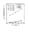
図7を参照して、下部電極のAlとTiとの含有量の好適値について説明する。下部電極のAlとTiとの含有量を変えて複数の試料を作製し、Al2O3下部副誘電体膜の厚さを測定した。 With reference to FIG. 7, the suitable value of content of Al and Ti of a lower electrode is demonstrated. A plurality of samples were prepared by changing the contents of Al and Ti in the lower electrode, and the thickness of the Al 2 O 3 lower subdielectric film was measured.
図7に、下部副誘電体膜を形成するためのアニール温度と、Al2O3下部副誘電体膜の厚さとの関係を示す。横軸はアニール温度を単位「℃」で表し、縦軸は、形成されたAl2O3下部副誘電体膜の厚さを単位「nm」で表す。アニール温度を600℃よりも高くすると、Al2O3、及びTa2O5が結晶化してしまうため、アニール温度は400℃〜600℃の範囲内で変化させた。アニール時間は60秒とした。 FIG. 7 shows the relationship between the annealing temperature for forming the lower subdielectric film and the thickness of the Al 2 O 3 lower subdielectric film. The horizontal axis represents the annealing temperature in the unit “° C.”, and the vertical axis represents the thickness of the formed Al 2 O 3 lower subdielectric film in the unit “nm”. When the annealing temperature was higher than 600 ° C., Al 2 O 3 and Ta 2 O 5 were crystallized, so the annealing temperature was changed within the range of 400 ° C. to 600 ° C. The annealing time was 60 seconds.
図中の菱形、正方形、三角、及びエックス記号は、それぞれTiに対するAlの含有量の比Al/Ti=20原子%、30原子%、50原子%、及び60原子%のAlTi合金ターゲットを用いてTiAlN膜を形成した試料における下部副誘電体膜の厚さを示す。なお、実際に形成されるTiAlN膜のAlとTiの含有量の比は、AlTi合金ターゲットのAlとTiの含有量の比とほぼ等しい。 The rhombus, square, triangle, and X symbols in the figure use AlTi alloy targets of Al / Ti = 20 atomic%, 30 atomic%, 50 atomic%, and 60 atomic%, respectively. The thickness of the lower subdielectric film in the sample on which the TiAlN film is formed is shown. Note that the ratio of the Al and Ti contents of the TiAlN film that is actually formed is substantially equal to the ratio of the Al and Ti contents of the AlTi alloy target.
図5A及び図5Bに示した評価結果から、下部副誘電体膜の厚さは0.5nm以上にすることが好ましい。Al/Ti=20原子%のAlTi合金ターゲットを用いると、アニール温度を600℃まで高くしても、0.5nm以上の厚さのAl2O3膜が形成されない。これは、アニール時に、下部電極から十分な量のAlが供給されないためであると考えられる。十分な厚さのAl2O3下部副誘電体膜を形成するために、下部電極膜のTiAlNのアニール前におけるTiに対するAlの含有量の比Al/Tiを30原子%以上にすることが好ましい。 From the evaluation results shown in FIGS. 5A and 5B, the thickness of the lower subdielectric film is preferably 0.5 nm or more. When an AlTi alloy target of Al / Ti = 20 atomic% is used, an Al 2 O 3 film having a thickness of 0.5 nm or more is not formed even when the annealing temperature is increased to 600 ° C. This is considered to be because a sufficient amount of Al is not supplied from the lower electrode during annealing. In order to form a sufficiently thick Al 2 O 3 lower subdielectric film, it is preferable that the ratio Al / Ti of Ti to Ti before annealing of TiAlN in the lower electrode film is 30 atomic% or more. .
また、含有量の比Al/Tiを60原子%にすると、Al2O3膜の成膜速度が速くなりすぎ、膜厚の制御が困難になる。Al2O3下部副誘電体膜の膜厚の制御性を高くするために、TiAlN下部電極膜のアニール前におけるTiに対するAlの含有量の比Al/Tiを50原子%以下とすることが好ましい。 On the other hand, when the content ratio Al / Ti is set to 60 atomic%, the deposition rate of the Al 2 O 3 film becomes too fast, and the control of the film thickness becomes difficult. In order to increase the controllability of the film thickness of the Al 2 O 3 lower subdielectric film, the ratio of Al content to Ti before annealing of the TiAlN lower electrode film is preferably 50 atomic% or less. .
図8A及び図8Bを参照して、アニールを行う好適な時期について説明する。図1A〜図1Fに示した実施例では、Al2O3上部副誘電体膜32を形成した後にアニールを行った。その他に、TiAlN下部電極膜30を形成した直後、Ta2O5主誘電体膜31を形成した直後、及びTiN上部電極膜38を形成した直後のいずれかにアニールを行った複数の試料を作製した。
With reference to FIG. 8A and FIG. 8B, the suitable time for performing annealing will be described. In the embodiment shown in FIGS. 1A to 1F, annealing was performed after the Al 2 O 3
図8Aに、アニール温度とキャパシタ容量との関係を示し、図8Bに、アニール温度とリーク電流との関係を示す。図8A及び図8Bの横軸は、アニール温度を単位「℃」で表し、図8Aの縦軸は単位面積当たりのキャパシタ容量を単位「fF/μm2」で表し、図8Bの縦軸は、単位面積当たりのリーク電流を単位「fA/μm2」で表す。図中の菱形、正方形、三角、及びエックス記号は、それぞれTiAlN下部電極膜形成直後、Ta2O5主誘電体膜形成直後、Al2O3上部副誘電体膜形成直後、及びTiN上部電極膜形成直後にアニールを行った試料の測定結果を示す。 FIG. 8A shows the relationship between the annealing temperature and the capacitor capacity, and FIG. 8B shows the relationship between the annealing temperature and the leakage current. 8A and 8B, the horizontal axis represents the annealing temperature in the unit “° C.”, the vertical axis in FIG. 8A represents the capacitor capacity per unit area in the unit “fF / μm 2 ”, and the vertical axis in FIG. The leakage current per unit area is represented by the unit “fA / μm 2 ”. The rhombus, square, triangle, and X symbol in the figure are respectively immediately after the formation of the TiAlN lower electrode film, immediately after the formation of the Ta 2 O 5 main dielectric film, immediately after the formation of the Al 2 O 3 upper subdielectric film, and the TiN upper electrode film. The measurement result of the sample which annealed immediately after formation is shown.
TiAlN下部電極膜を形成した後、Ta2O5主誘電体膜を形成する前にアニールを行った試料は、他の試料に比べて大きなキャパシタ容量が得られているが、リーク電流も多い。これは、TiAlN下部電極膜の表面が、アニール雰囲気中に残留する酸素によって酸化され、酸化に起因する荒れが生じているためと考えられる。なお、TiN表面が露出している場合には、同一の条件でアニールを行っても、酸化は生じない。TiAlN下部電極膜を形成した後、Ta2O5主誘電体膜を形成する前にアニールを行った試料では、表面に析出するAlが酸化されるため、表面荒れが生じたと考えられる。 A sample subjected to annealing after forming the TiAlN lower electrode film and before forming the Ta 2 O 5 main dielectric film has a larger capacitor capacity than other samples, but also has a large leakage current. This is presumably because the surface of the TiAlN lower electrode film is oxidized by oxygen remaining in the annealing atmosphere, and roughening due to oxidation occurs. When the TiN surface is exposed, oxidation does not occur even if annealing is performed under the same conditions. In the sample that was annealed after the TiAlN lower electrode film was formed and before the Ta 2 O 5 main dielectric film was formed, Al deposited on the surface is oxidized, and it is considered that surface roughness has occurred.
また、Ta2O5主誘電体膜を形成した後は、いずれの段階でアニールを行っても、キャパシタ容量及びリーク電流に有意な差はない。従って、アニールは、Ta2O5主誘電体膜を形成した後、どの段階でおこなってもよい。 In addition, after the Ta 2 O 5 main dielectric film is formed, there is no significant difference in the capacitor capacity and the leakage current regardless of the stage of annealing. Therefore, annealing may be performed at any stage after the Ta 2 O 5 main dielectric film is formed.
図9に、アニール温度とAl2O3下部副誘電体膜の厚さとの関係を示す。図9に示した評価の対象となった試料は、Ta2O5主誘電体膜を形成した後に、アニールを行った。TiAlN下部電極膜のTiに対するAlの含有量の比Al/Tiは50原子%とした。アニール時間は60秒とした。 FIG. 9 shows the relationship between the annealing temperature and the thickness of the Al 2 O 3 lower subdielectric film. The sample to be evaluated shown in FIG. 9 was annealed after the Ta 2 O 5 main dielectric film was formed. The ratio of Al content to Ti in the TiAlN lower electrode film was 50 atomic%. The annealing time was 60 seconds.
アニール温度が350℃以下の場合には、下部副誘電体膜の厚さを0.5nm以上にすることが困難である。このため、図5Bに示した評価結果からわかるように、リーク電流が多くなってしまう。リーク電流の増大を防止するために、アニール温度を400℃以上にすることが好ましい。また、アニール温度を600℃よりも高くすると、Al2O3やTa2O5が結晶化してしまう。従って、アニール温度を600℃以下にすることが好ましい。 When the annealing temperature is 350 ° C. or less, it is difficult to make the thickness of the lower subdielectric film 0.5 nm or more. For this reason, as can be seen from the evaluation result shown in FIG. 5B, the leakage current increases. In order to prevent an increase in leakage current, the annealing temperature is preferably set to 400 ° C. or higher. Further, when the annealing temperature is higher than 600 ° C., Al 2 O 3 and Ta 2 O 5 are crystallized. Therefore, it is preferable that the annealing temperature is 600 ° C. or lower.
上記実施例では、導電プラグ20の直上に配置したいわゆるスタック構造のMIMキャパシタについて説明したが、上記実施例は、プレーナ構造のMIMキャパシタにも適用可能である。
In the above embodiment, a so-called stack structure MIM capacitor disposed immediately above the
図10に、プレーナ構造のMIMキャパシタの断面図を示す。以下、図1Fに示したスタック構造のMIMキャパシタとの相違点に着目して説明する。 FIG. 10 shows a cross-sectional view of a planar structure MIM capacitor. Hereinafter, the description will be given focusing on the difference from the MIM capacitor having the stack structure shown in FIG. 1F.
プレーナ構造のMIMキャパシタにおいては、下部副誘電体膜35aから上部電極38aまでの積層構造の平面形状が、下部電極30aの平面形状よりも小さくされている。スタック構造のMIMキャパシタにおいては、下部電極30aが、その下方に配置された導電プラグ20に接続されていたが、プレーナ構造では、MIMキャパシタの直下には導電プラグが配置されない。その代わりに、下部電極30aは、上部電極38aの脇を通過する導電プラグ38に接続される。
In the planar structure MIM capacitor, the planar shape of the laminated structure from the
プレーナ構造においても、Al2O3下部副誘電体膜35aは、Ta2O5主誘電体膜31aを形成した後のアニールにより、形成される。このため、スタック構造の実施例と同様に、キャパシタ容量を大きく保ったまま、リーク電流の増大を防止することができる。
Also in the planar structure, the Al 2 O 3
また、上記実施例では、TiAlN下部電極膜30とTa2O5主誘電体膜31との間の下部副誘電体膜35を、アニールにより形成したが、上部副誘電体膜32をアニールにより形成してもよいし、下部と上部の両方のAl2O3誘電体膜35、32をアニールにより形成してもよい。上部副誘電体膜32をアニールで形成する場合には、Ta2O5主誘電体膜31の上に、TiAlN上部電極膜38を形成し、その後アニールを行えばよい。主誘電体膜31内のOと上部電極膜38内のAlとが反応することにより、両者の界面にAl2O3からなる上部副誘電体膜32が形成される。
In the above embodiment, the
上記実施例では、下部電極膜30の材料を「TiAlN」と表記したが、実施例中の説明から、この表記は、TiとAlとNとの組成比が1:1:1であることを意味していないことは明らかである。同様に、上部電極膜38の材料を「TiN」と表記したが、この表記は、TiとNとの組成比が1:1であることを意味していない。さらに、上記実施例では、誘電体膜の材料に「Al2O3」、「Ta2O5」という表記を用いたが、実際に形成される誘電体膜の元素組成比じゃ、化学量論的組成比に一致するとは限らない。実際の誘電体膜の元素組成比が化学量論的組成比からずれたとしても、上記実施例で説明した効果と同等の効果を得ることができる。
In the above embodiment, the material of the
以上実施例に沿って本発明を説明したが、本発明はこれらに制限されるものではない。例えば、種々の変更、改良、組み合わせ等が可能なことは当業者に自明であろう。 Although the present invention has been described with reference to the embodiments, the present invention is not limited thereto. It will be apparent to those skilled in the art that various modifications, improvements, combinations, and the like can be made.
10 半導体基板
11 素子分離絶縁膜
12 MISFET
15、17、19 層間絶縁膜
16、20 導電プラグ
18 配線
30 下部電極膜
30a 下部電極
31、31a 主誘電体膜
32、32a 上部副誘電体膜
35、35a 下部副誘電体膜
38 上部電極膜
38a 上部電極
40 MIMキャパシタ
45 層間絶縁膜
46、48 導電プラグ
10
15, 17, 19
Claims (8)
前記第1の電極膜と前記主誘電体膜とが形成されている状態でアニールを行うことにより、前記第1の電極膜中のアルミニウムと前記主誘電体膜中の酸素とを反応させて、前記第1の電極膜と前記主誘電体膜との界面に、酸化アルミニウムを含む副誘電体膜を形成する工程と、
前記主誘電体膜と前記副誘電体膜とを介して前記第1の電極膜に対向する位置に第2の電極膜を形成する工程と
を有する半導体装置の製造方法。 Forming a first electrode film containing TiAlN and a main dielectric film containing tantalum oxide on a semiconductor substrate;
By performing annealing in a state where the first electrode film and the main dielectric film are formed, the aluminum in the first electrode film reacts with the oxygen in the main dielectric film, Forming a sub-dielectric film containing aluminum oxide at the interface between the first electrode film and the main dielectric film;
Forming a second electrode film at a position opposed to the first electrode film via the main dielectric film and the sub-dielectric film.
Priority Applications (2)
| Application Number | Priority Date | Filing Date | Title |
|---|---|---|---|
| JP2008164701A JP5458514B2 (en) | 2008-06-24 | 2008-06-24 | Semiconductor device manufacturing method and semiconductor device |
| US12/365,276 US8003462B2 (en) | 2008-06-24 | 2009-02-04 | Manufacture method for semiconductor device having MIM capacitor, and semiconductor device |
Applications Claiming Priority (1)
| Application Number | Priority Date | Filing Date | Title |
|---|---|---|---|
| JP2008164701A JP5458514B2 (en) | 2008-06-24 | 2008-06-24 | Semiconductor device manufacturing method and semiconductor device |
Publications (2)
| Publication Number | Publication Date |
|---|---|
| JP2010010211A true JP2010010211A (en) | 2010-01-14 |
| JP5458514B2 JP5458514B2 (en) | 2014-04-02 |
Family
ID=41431032
Family Applications (1)
| Application Number | Title | Priority Date | Filing Date |
|---|---|---|---|
| JP2008164701A Expired - Fee Related JP5458514B2 (en) | 2008-06-24 | 2008-06-24 | Semiconductor device manufacturing method and semiconductor device |
Country Status (2)
| Country | Link |
|---|---|
| US (1) | US8003462B2 (en) |
| JP (1) | JP5458514B2 (en) |
Families Citing this family (8)
| Publication number | Priority date | Publication date | Assignee | Title |
|---|---|---|---|---|
| WO2011034536A1 (en) * | 2009-09-18 | 2011-03-24 | Intermolecular, Inc. | Fabrication of semiconductor stacks with ruthenium-based materials |
| US8912061B2 (en) | 2011-06-28 | 2014-12-16 | International Business Machines Corporation | Floating gate device with oxygen scavenging element |
| US8541867B2 (en) * | 2011-06-28 | 2013-09-24 | International Business Machines Corporation | Metal insulator metal structure with remote oxygen scavenging |
| US8716088B2 (en) | 2012-06-27 | 2014-05-06 | International Business Machines Corporation | Scavenging metal stack for a high-K gate dielectric |
| FR2996679A1 (en) * | 2012-10-09 | 2014-04-11 | St Microelectronics Crolles 2 | METHOD FOR DEPOSITING A LOW-DIFFUSED TIALN LAYER AND ISOLATED GRID COMPRISING SUCH A LAYER |
| US20170040108A1 (en) * | 2015-08-06 | 2017-02-09 | Murata Manufacturing Co., Ltd. | Capacitor |
| US9564310B1 (en) | 2015-11-18 | 2017-02-07 | International Business Machines Corporation | Metal-insulator-metal capacitor fabrication with unitary sputtering process |
| US20210305356A1 (en) * | 2020-03-26 | 2021-09-30 | Taiwan Semiconductor Manufacturing Co., Ltd. | Barrier layer for metal insulator metal capacitors |
Citations (5)
| Publication number | Priority date | Publication date | Assignee | Title |
|---|---|---|---|---|
| JP2002164506A (en) * | 2000-11-27 | 2002-06-07 | Toshiba Corp | Semiconductor device and its manufacturing method |
| JP2004039728A (en) * | 2002-07-01 | 2004-02-05 | Toshiba Corp | Semiconductor device and its manufacturing method |
| JP2004134451A (en) * | 2002-10-08 | 2004-04-30 | Renesas Technology Corp | Semiconductor device and its manufacturing method |
| JP2004152796A (en) * | 2002-10-28 | 2004-05-27 | Toshiba Corp | Semiconductor device and its manufacturing method |
| JP2004214668A (en) * | 2002-12-31 | 2004-07-29 | Texas Instruments Inc | Mim capacitor and its manufacturing method |
Family Cites Families (2)
| Publication number | Priority date | Publication date | Assignee | Title |
|---|---|---|---|---|
| US6485988B2 (en) * | 1999-12-22 | 2002-11-26 | Texas Instruments Incorporated | Hydrogen-free contact etch for ferroelectric capacitor formation |
| US6475854B2 (en) * | 1999-12-30 | 2002-11-05 | Applied Materials, Inc. | Method of forming metal electrodes |
-
2008
- 2008-06-24 JP JP2008164701A patent/JP5458514B2/en not_active Expired - Fee Related
-
2009
- 2009-02-04 US US12/365,276 patent/US8003462B2/en not_active Expired - Fee Related
Patent Citations (5)
| Publication number | Priority date | Publication date | Assignee | Title |
|---|---|---|---|---|
| JP2002164506A (en) * | 2000-11-27 | 2002-06-07 | Toshiba Corp | Semiconductor device and its manufacturing method |
| JP2004039728A (en) * | 2002-07-01 | 2004-02-05 | Toshiba Corp | Semiconductor device and its manufacturing method |
| JP2004134451A (en) * | 2002-10-08 | 2004-04-30 | Renesas Technology Corp | Semiconductor device and its manufacturing method |
| JP2004152796A (en) * | 2002-10-28 | 2004-05-27 | Toshiba Corp | Semiconductor device and its manufacturing method |
| JP2004214668A (en) * | 2002-12-31 | 2004-07-29 | Texas Instruments Inc | Mim capacitor and its manufacturing method |
Also Published As
| Publication number | Publication date |
|---|---|
| US20090316331A1 (en) | 2009-12-24 |
| JP5458514B2 (en) | 2014-04-02 |
| US8003462B2 (en) | 2011-08-23 |
Similar Documents
| Publication | Publication Date | Title |
|---|---|---|
| JP5458514B2 (en) | Semiconductor device manufacturing method and semiconductor device | |
| EP1368822B1 (en) | Rhodium-rich oxygen barriers | |
| KR100818058B1 (en) | Method for forming mim capacitor | |
| US6140671A (en) | Semiconductor memory device having capacitive storage therefor | |
| US9887083B2 (en) | Methods of forming capacitors | |
| TWI401745B (en) | Semiconductor device and manufacturing method thereof | |
| JP5883263B2 (en) | Method for producing metal-insulator-metal capacitor used in semiconductor device | |
| JP3943033B2 (en) | Capacitor and manufacturing method thereof | |
| US6559000B2 (en) | Method of manufacturing a capacitor in a semiconductor device | |
| JP4571836B2 (en) | Semiconductor device and manufacturing method thereof | |
| JP2009239047A (en) | Capacitor structure with zirconium nitride interface layer | |
| US20100164064A1 (en) | Capacitor and Method for Manufacturing the Same | |
| US6365487B2 (en) | Method of manufacturing a capacitor in a semiconductor device | |
| JP2003017581A (en) | Semiconductor device and its manufacturing method | |
| JP4088913B2 (en) | Capacitor manufacturing method for semiconductor device | |
| JP2004039728A (en) | Semiconductor device and its manufacturing method | |
| US6653198B2 (en) | Method for fabricating capacitor in semiconductor device and capacitor fabricated thereby | |
| US6407419B1 (en) | Semiconductor device and manufacturing method thereof | |
| JP2003174092A (en) | Semiconductor device and method of manufacturing the same | |
| JP5955045B2 (en) | Semiconductor device manufacturing method and semiconductor device | |
| JP2000307069A (en) | Manufacture of semiconductor device | |
| KR100585003B1 (en) | Capacitor and method for fabricating the same | |
| KR100683489B1 (en) | Method for forming a capacitor in semiconductor device | |
| KR20070098275A (en) | Method of manufacturing a capacitor of semiconductor device | |
| KR20020002755A (en) | Method of forming a capacitor in a semiconductor device |
Legal Events
| Date | Code | Title | Description |
|---|---|---|---|
| A621 | Written request for application examination |
Free format text: JAPANESE INTERMEDIATE CODE: A621 Effective date: 20110125 |
|
| A977 | Report on retrieval |
Free format text: JAPANESE INTERMEDIATE CODE: A971007 Effective date: 20130301 |
|
| A131 | Notification of reasons for refusal |
Free format text: JAPANESE INTERMEDIATE CODE: A131 Effective date: 20130409 |
|
| A521 | Request for written amendment filed |
Free format text: JAPANESE INTERMEDIATE CODE: A523 Effective date: 20130528 |
|
| TRDD | Decision of grant or rejection written | ||
| A01 | Written decision to grant a patent or to grant a registration (utility model) |
Free format text: JAPANESE INTERMEDIATE CODE: A01 Effective date: 20131217 |
|
| A61 | First payment of annual fees (during grant procedure) |
Free format text: JAPANESE INTERMEDIATE CODE: A61 Effective date: 20131230 |
|
| R150 | Certificate of patent or registration of utility model |
Ref document number: 5458514 Country of ref document: JP Free format text: JAPANESE INTERMEDIATE CODE: R150 Free format text: JAPANESE INTERMEDIATE CODE: R150 |
|
| S531 | Written request for registration of change of domicile |
Free format text: JAPANESE INTERMEDIATE CODE: R313531 |
|
| R350 | Written notification of registration of transfer |
Free format text: JAPANESE INTERMEDIATE CODE: R350 |
|
| S111 | Request for change of ownership or part of ownership |
Free format text: JAPANESE INTERMEDIATE CODE: R313111 |
|
| R350 | Written notification of registration of transfer |
Free format text: JAPANESE INTERMEDIATE CODE: R350 |
|
| LAPS | Cancellation because of no payment of annual fees |