JP2010008535A - Image display device - Google Patents
Image display device Download PDFInfo
- Publication number
- JP2010008535A JP2010008535A JP2008165474A JP2008165474A JP2010008535A JP 2010008535 A JP2010008535 A JP 2010008535A JP 2008165474 A JP2008165474 A JP 2008165474A JP 2008165474 A JP2008165474 A JP 2008165474A JP 2010008535 A JP2010008535 A JP 2010008535A
- Authority
- JP
- Japan
- Prior art keywords
- luminance
- video signal
- video
- unit
- histogram
- Prior art date
- Legal status (The legal status is an assumption and is not a legal conclusion. Google has not performed a legal analysis and makes no representation as to the accuracy of the status listed.)
- Granted
Links
Images


Abstract
Description
本発明は、映像表示装置に関し、フレームレートあるいはフィールドレートを変換する機能を備えた映像表示装置に関する。 The present invention relates to a video display device, and more particularly to a video display device having a function of converting a frame rate or a field rate.
従来、液晶表示装置のようなホールド型表示方式における動きぼけを改善するために、フレーム間に画像を内挿することにより、フレームレート(フレーム数)を変換する技術が知られている。この技術はFRC(Frame Rate Converter)と呼ばれ、液晶表示装置等において実用化されている。 Conventionally, a technique for converting a frame rate (the number of frames) by interpolating an image between frames in order to improve motion blur in a hold-type display method such as a liquid crystal display device is known. This technique is called FRC (Frame Rate Converter) and is put into practical use in liquid crystal display devices and the like.
例えば、特許文献1には、動き適応的に内挿フレームを生成することにより、表示画像のフレーム周波数を上げて、動きぼけの原因となる空間周波数特性の低下を改善するための技術が記載されている。これは、表示画像のフレーム間に内挿する少なくとも1つの内挿画像信号を、前後のフレームから動き適応的に形成し、形成した内挿画像信号をフレーム間に内挿して順次表示するようにしている。 For example, Patent Document 1 describes a technique for improving a decrease in spatial frequency characteristics that causes motion blur by increasing the frame frequency of a display image by generating an interpolation frame adaptively in motion. ing. In this method, at least one interpolated image signal to be interpolated between frames of a display image is formed in a motion adaptive manner from the preceding and following frames, and the formed interpolated image signal is interpolated between frames and sequentially displayed. ing.
一方、最近の映像表示装置では、特に液晶表示装置において、入力映像信号のゲイン制御を行うだけでなく、入力映像信号のゲイン制御と連動してバックライト光源の発光輝度を変調させることにより、消費電力を低減させるとともに、よりコントラスト感を高める技術が提案されている。 On the other hand, in recent video display devices, particularly in liquid crystal display devices, not only gain control of the input video signal, but also by modulating the luminance of the backlight light source in conjunction with the gain control of the input video signal, Techniques have been proposed for reducing power and enhancing contrast.
例えば、特許文献2,3には、映像信号のヒストグラムが表示可能帯域の所定比率以下である場合(輝度分布が暗い場合)に、バックライトの輝度を落とすとともに、入力映像信号のゲインを上げて、映像表示輝度を保ちながらコントラスト感の向上を図ることが記載されている。特に、特許文献3では、入力映像信号のゲインを上げたことによる白つぶれを生じさせないようにするために、高階調領域に対して非線形の補正を行うことが記載されている。 For example, in Patent Documents 2 and 3, when the histogram of the video signal is equal to or less than a predetermined ratio of the displayable band (when the luminance distribution is dark), the backlight luminance is decreased and the gain of the input video signal is increased. Further, it is described to improve the contrast while maintaining the video display luminance. In particular, Patent Document 3 describes that non-linear correction is performed on a high gradation region so as not to cause whitening caused by increasing the gain of an input video signal.
さらに、特許文献4には、映像信号の最大輝度レベル、最小輝度レベル、平均輝度レベルに応じて入力信号をダイナミックレンジ幅までゲインを上げるとともに、バックライトの輝度を調節することが記載されている。 Furthermore, Patent Document 4 describes that the gain of an input signal is increased to the dynamic range width and the luminance of the backlight is adjusted according to the maximum luminance level, minimum luminance level, and average luminance level of the video signal. .
このように、上記特許文献2〜4に記載の技術によれば、全体的に暗い映像が入力された場合に、バックライトの発光輝度を下げて、入力映像信号のゲインを上げることで、ピーク輝度を同等に保ちながら、省電力化を実現し、コントラスト感の向上を図ることができる。
前述のFRC処理においては、シーンチェンジが有った場合に動きベクトルを初期化することが行われている。これはシーンが変化した場合、現画面と前画面との相関が少ないため、前画面との間で動き補償を行うと不自然な画像となってしまうためである。このようなシーンチェンジを検出するための一つの手段として、一般に映像信号のAPL(平均輝度レベル)が用いられている。このAPLは映像の輝度値の加算によって比較的容易に算出することができる。従来の映像表示装置では、APLの変化が大きければ、シーンチェンジが有ったものと判定し、FRC処理時に動きベクトルを初期化していた。 In the FRC process described above, a motion vector is initialized when there is a scene change. This is because when the scene changes, there is little correlation between the current screen and the previous screen, and therefore, when motion compensation is performed between the current screen and the previous screen, an unnatural image is obtained. As one means for detecting such a scene change, APL (average luminance level) of a video signal is generally used. This APL can be calculated relatively easily by adding the luminance values of the video. In the conventional video display device, if the change in APL is large, it is determined that there is a scene change, and the motion vector is initialized during the FRC process.
しかしながら、シーンチェンジを検出する手段として、上記のAPLを用いた場合、シーンが変化しても、たまたまAPLが同一であると、映像表示装置ではシーンチェンジがなかったものと判定してしまい、動きベクトルを初期化せず、画質を劣化させてしまうという問題があった。 However, when the above APL is used as a means for detecting a scene change, even if the scene changes, if the APL happens to be the same, the video display device determines that there is no scene change and moves There is a problem that the image quality is deteriorated without initializing the vector.
また、特許文献2〜4に記載されているような輝度変調処理では、字幕等の白ピークの有無により輝度変調処理後のAPLが大きく変化することになる。字幕等の白ピークを含む映像の場合、映像信号は0から255までの値を持つため、映像信号のゲインを変化させることはない。一方、白ピークを含まない暗い映像の場合、映像信号のゲインを変化させて0から255まで拡張し、その分バックライト輝度を下げる制御を行う。このため、同じようなシーンであっても、字幕等の白ピークの有無によりAPLが大きく変化することになる。 In the luminance modulation processing described in Patent Documents 2 to 4, the APL after the luminance modulation processing changes greatly depending on the presence or absence of a white peak such as caption. In the case of a video including a white peak such as caption, the video signal has a value from 0 to 255, and thus the gain of the video signal is not changed. On the other hand, in the case of a dark image that does not include a white peak, the gain of the image signal is changed and extended from 0 to 255, and the backlight luminance is controlled to be reduced accordingly. For this reason, even in a similar scene, the APL greatly changes depending on the presence or absence of a white peak such as a caption.
上記の輝度変調処理と共に、FRC処理を行う構成とした場合、FRC回路内で輝度変調処理後の映像信号のAPLに基づいてシーンチェンジが検出される。従って、同じようなシーンであっても、白ピークの有無により輝度変調処理後のAPLが大きく変化してしまうと、映像表示装置はこのAPLの変化に基づいてシーンチェンジ有りと判定し、FRC処理時に動きベクトルを初期化してしまっていた。 When the FRC process is performed together with the luminance modulation process, a scene change is detected based on the APL of the video signal after the luminance modulation process in the FRC circuit. Therefore, even if the scene is similar, if the APL after the luminance modulation processing changes greatly due to the presence or absence of a white peak, the video display apparatus determines that there is a scene change based on the change in the APL, and performs FRC processing. Sometimes the motion vector was initialized.
本発明は、上述のごとき実情に鑑みてなされたものであり、動き補償型のFRC処理を行う際に、シーンチェンジを精度良く判定し、適切なFRC処理を行える映像表示装置を提供すること、を目的とする。 The present invention has been made in view of the above circumstances, and provides a video display device capable of accurately determining a scene change and performing appropriate FRC processing when performing motion compensation type FRC processing. With the goal.
上記課題を解決するために、本発明の第1の技術手段は、入力映像信号のフレーム間あるいはフィールド間に、動き補償処理を施した映像信号を内挿することにより、前記入力映像信号のフレーム数あるいはフィールド数を変換して表示パネルへ出力するレート変換手段を備えた映像表示装置であって、前記入力映像信号のヒストグラムに基づいてシーンチェンジか否かを検出するシーンチェンジ検出手段を備え、前記レート変換手段は、前記シーンチェンジ検出手段によりシーンチェンジが検出された場合に、動きベクトルを初期化することを特徴としたものである。 In order to solve the above-mentioned problem, the first technical means of the present invention interpolates a video signal subjected to motion compensation processing between frames or fields of an input video signal, so that a frame of the input video signal is obtained. A video display device comprising rate conversion means for converting the number or number of fields and outputting to the display panel, comprising scene change detection means for detecting whether or not a scene change is based on a histogram of the input video signal, The rate conversion means initializes a motion vector when a scene change is detected by the scene change detection means.
第2の技術手段は、第1の技術手段において、前記シーンチェンジ検出手段は、前記入力映像信号のフレーム間あるいはフィールド間におけるヒストグラムの変化量が所定値よりも大きい場合に、シーンチェンジと判定することを特徴としたものである。 According to a second technical means, in the first technical means, the scene change detecting means determines a scene change when the amount of change of the histogram between frames or fields of the input video signal is larger than a predetermined value. It is characterized by that.
第3の技術手段は、第1又は第2の技術手段において、前記レート変換手段は、前記入力映像信号に含まれる連続したフレーム間あるいはフィールド間で動きベクトル情報を検出する動きベクトル検出部と、該検出した動きベクトル情報に基づいて、前記フレーム間あるいは前記フィールド間に内挿ベクトルを割り付ける内挿ベクトル割付部と、該割り付けた内挿ベクトルから内挿映像信号を生成する内挿映像生成部と、該生成した内挿映像信号を前記フレーム間あるいは前記フィールド間に内挿する映像内挿部とを備えたことを特徴としたものである。 According to a third technical means, in the first or second technical means, the rate conversion means detects a motion vector information between successive frames or fields included in the input video signal, and Based on the detected motion vector information, an interpolation vector allocating unit that allocates an interpolation vector between the frames or between the fields, and an interpolation video generating unit that generates an interpolation video signal from the allocated interpolation vector; And a video interpolating unit for interpolating the generated interpolated video signal between the frames or the fields.
第4の技術手段は、第1〜第3のいずれか1の技術手段において、バックライトの発光輝度と入力映像信号のゲインとを連動して制御する輝度変調手段を備えたことを特徴としたものである。 According to a fourth technical means, in any one of the first to third technical means, there is provided luminance modulation means for controlling the light emission luminance of the backlight and the gain of the input video signal in conjunction with each other. Is.
本発明によれば、動き補償型のFRC処理を行う際に、入力映像信号のヒストグラムに基づいてシーンチェンジを精度良く判定することができるため、適切なFRC処理を行うことができる。 According to the present invention, when a motion compensation type FRC process is performed, a scene change can be accurately determined based on a histogram of an input video signal, so that an appropriate FRC process can be performed.
以下、添付図面を参照しながら、本発明の映像表示装置に係る好適な実施の形態について説明する。本実施形態における映像表示装置(以下、液晶表示装置で代表する)は、バックライト光源の発光輝度レベルと入力映像信号のゲインとを連動して制御する輝度変調部と、動き補償によりフレームレートあるいはフィールドレートを変換するFRC部とを備えるものとする。なお、本発明は、フィールド信号及び内挿フィールド信号、フレーム信号及び内挿フレーム信号のいずれに対しても適用できるものであるが、両者(フィールドとフレーム)は互いに類似の関係にあるため、フレーム信号及び内挿フレーム信号を代表例として説明するものとする。 DESCRIPTION OF EXEMPLARY EMBODIMENTS Hereinafter, preferred embodiments according to a video display device of the invention will be described with reference to the accompanying drawings. The video display device in this embodiment (hereinafter represented by a liquid crystal display device) includes a luminance modulation unit that controls the emission luminance level of a backlight light source and the gain of an input video signal in conjunction with each other, a frame rate or An FRC unit that converts a field rate is provided. Although the present invention can be applied to any of a field signal, an interpolated field signal, a frame signal, and an interpolated frame signal, both (field and frame) are in a similar relationship with each other, so A signal and an interpolated frame signal will be described as representative examples.
〈本発明に係る輝度変調処理の概要〉
液晶表示装置から発せられる光量は、表示する映像信号のレベルを忠実に再現するのが理想である。つまり、黒画面を表示する場合、画面から発せられる光量は理想的には0でなければならない。しかし、現実の液晶表示装置では、若干の光漏れがあり、黒画面を表示する場合にも黒ではなくグレー表示となる。
<Outline of Luminance Modulation Processing According to the Present Invention>
Ideally, the amount of light emitted from the liquid crystal display device faithfully reproduces the level of the video signal to be displayed. That is, when displaying a black screen, the amount of light emitted from the screen should ideally be zero. However, in an actual liquid crystal display device, there is some light leakage, and even when a black screen is displayed, gray display is performed instead of black.
液晶表示装置の重要な性能の一つとしてコントラスト比(以下CRともいう)がある。液晶表示装置において、CRは表示パネル上の最大輝度と最小輝度の比である。液晶表示装置の場合、最大輝度は光源の最大発光輝度で決まり、最小輝度は黒表示時の光漏れ量によって決まる。よって、光源の発光輝度が一定の場合、同一の液晶パネルにおいてコントラスト比は一定となる。 One important performance of a liquid crystal display device is a contrast ratio (hereinafter also referred to as CR). In the liquid crystal display device, CR is a ratio between the maximum luminance and the minimum luminance on the display panel. In the case of a liquid crystal display device, the maximum luminance is determined by the maximum light emission luminance of the light source, and the minimum luminance is determined by the amount of light leakage during black display. Therefore, when the light emission luminance of the light source is constant, the contrast ratio is constant in the same liquid crystal panel.
図1は、CRが3000と6000の液晶パネルについて、入力階調(映像信号レベル)と液晶パネル上での輝度値との関係を示すグラフである。最大輝度は共に同じ450cdであるが、入力階調(画素値)0での液晶パネル上の表示輝度(最小輝度)はCR3000の場合に0.15cd、CR6000の場合に0.075cdとなり、2倍の差がある。 FIG. 1 is a graph showing the relationship between the input gradation (video signal level) and the luminance value on the liquid crystal panel for liquid crystal panels with CR of 3000 and 6000. The maximum brightness is the same 450 cd, but the display brightness (minimum brightness) on the liquid crystal panel at the input gradation (pixel value) 0 is 0.15 cd in the case of CR3000 and 0.075 cd in the case of CR6000. There is a difference.
ここで、CR3000の液晶パネル使用時に光源の発光輝度を50%まで下げるとともにゲイン設定で入力映像信号を所定量増幅させると、入力映像信号の画素値と液晶パネルの表示輝度値との関係は、図1において点線で示すような関係となり、画素値0〜128においてはCR6000の液晶パネルに近い輝度表現をさせることが可能となる。しかしながら、画素値128より大きい映像は階調表現できず、いわゆる白つぶれを起こすことになる。従って、入力映像信号の特徴量に応じてバックライトの発光輝度の調節と、ゲイン設定を行う必要がある。 Here, when the light emission luminance of the light source is reduced to 50% and the input video signal is amplified by a predetermined amount when the CR3000 liquid crystal panel is used, the relationship between the pixel value of the input video signal and the display luminance value of the liquid crystal panel is The relationship is as shown by the dotted line in FIG. 1, and a luminance expression close to that of a CR6000 liquid crystal panel can be obtained with pixel values of 0 to 128. However, an image with a pixel value greater than 128 cannot be expressed in gradation, and so-called whitening occurs. Therefore, it is necessary to adjust the light emission luminance of the backlight and set the gain according to the feature amount of the input video signal.
例えば、入力映像信号の輝度のヒストグラムが画素値128以下の輝度分布を示す場合に、上述の図1で示すようにバックライトの輝度を50%まで下げるとともにゲイン設定で所定の入力映像信号を所定量増幅させるような制御を行うようにすればよい。このように入力映像信号の特徴量に応じてバックライトの発光輝度の制御及びゲイン設定を行うことにより、コントラスト感を高めることができると同時にバックライトの発光輝度を下げることによる省電力化を図ることが可能となる。 For example, when the luminance histogram of the input video signal indicates a luminance distribution with a pixel value of 128 or less, the backlight luminance is reduced to 50% as shown in FIG. Control that allows quantitative amplification may be performed. By controlling the backlight emission luminance and setting the gain in accordance with the feature amount of the input video signal in this way, it is possible to increase the contrast feeling and at the same time to save power by lowering the backlight emission luminance. It becomes possible.
上記では入力映像信号の輝度のヒストグラムが画素値128以下の輝度分布を示す場合を例に挙げ説明したが、上記例以外でも、例えば、映像中の白部分が極めて少ない場合には、白部分の重視度を下げ、黒表現の向上を同様にして図ることができる。このとき、重視しない部分の白つぶれは無視してもよいし、ターゲットCRを実現させるゲイン設定によっても白つぶれが緩和できるように、白側領域でのゲインを決めるようにしてもよい。 In the above description, the case where the luminance histogram of the input video signal shows a luminance distribution with a pixel value of 128 or less has been described as an example. However, other than the above example, for example, when the white portion in the video is extremely small, The degree of importance can be lowered and black expression can be improved in the same manner. At this time, the unsharp portions of the white area may be ignored, or the gain in the white area may be determined so that the white area can be reduced by the gain setting for realizing the target CR.
また、本発明に係る輝度変調処理では、省電力化を図るために、後述するように映像信号から得た映像のAPL等の特徴量に応じて動的に光源の発光輝度を抑える処理も併せて実行する。
つまり、ゲイン設定及びバックライト光源の発光輝度レベルを設定するための参照用の発光輝度レベルをまず映像特徴量(APL,ピーク(最大輝度値),ヒストグラム情報等)に応じて設定し、省電力化を図ると共に、参照用の発光輝度レベルに対して、さらに上述のごときコントラスト感を出すための処理(すなわち発光輝度レベルを参照用の発光輝度レベル以下の適切な値に設定する)を実行して、CR向上及び更なる省電力化を図り、その処理と連動させて映像信号のゲインを設定して、視覚上の輝度を保つようにする。
In addition, in the luminance modulation processing according to the present invention, in order to save power, processing for dynamically suppressing the light emission luminance of the light source according to the feature amount such as APL of the video obtained from the video signal as described later is also performed. And execute.
In other words, the reference emission luminance level for setting the gain setting and the emission luminance level of the backlight light source is first set in accordance with the video feature amount (APL, peak (maximum luminance value), histogram information, etc.), thereby saving power. In addition, a process for producing a contrast feeling as described above (that is, setting the light emission luminance level to an appropriate value equal to or lower than the reference light emission luminance level) is performed on the reference light emission luminance level. Thus, the CR is improved and further power saving is performed, and the gain of the video signal is set in conjunction with the processing so as to maintain the visual luminance.
〈本発明に係る輝度変調処理を行う液晶表示装置のシステム構成例〉
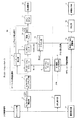
図2は、本発明に係る液晶表示装置のシステム構成例を示すブロック図である。図2で例示する液晶表示装置は、スケーリング部1、Yヒストグラム検出部2、APL検出部3、BL(バックライト)輝度レベル設定部8、CPU(Central Processing Unit)/CPLD(Complex Programmable Logic Device)11、BL調整部12、画質補正部14、RGBγ/WB(White Balance)調整部15、FRC(Frame Rate Control)部16、及び映像出力部17を備える。
<System configuration example of a liquid crystal display device that performs luminance modulation processing according to the present invention>
FIG. 2 is a block diagram showing a system configuration example of the liquid crystal display device according to the present invention. The liquid crystal display device illustrated in FIG. 2 includes a scaling unit 1, a Y histogram detection unit 2, an APL detection unit 3, a BL (backlight) luminance
図2で例示する液晶表示装置は、さらに本発明に係る輝度変調処理の主な部分を実行するアドバンスト輝度変調部20を備える。アドバンスト輝度変調部20は、本発明の輝度変調手段に相当し、ヒストグラムストレッチング部4、ディストーションモジュール5、シーンチェンジ検出部6、第1のテンポラリフィルタ7、第2のテンポラリフィルタ9、可変ディレイ10、コンフィグレーションデザイン部13を有する。なお、上述したように、本発明に係る輝度変調処理は、APL等の特徴量に応じた動的な光源の発光輝度制御を行うだけでなく、その映像特徴量の所定の条件により決定される光源の参照用の発光輝度レベルBLrefに対しさらにコントラスト感を出すような発光輝度レベルBLreducedを選択し、且つ映像信号のゲインも設定するという進化した輝度変調処理である。そのため、この処理を実行する部位を「アドバンスト」輝度変調部20と呼んでいる。
The liquid crystal display device illustrated in FIG. 2 further includes an advanced
まず、図2の液晶表示装置における各ブロックの概要について説明する。
映像出力部17は、映像信号による映像を表示する液晶パネルと、映像信号を液晶パネル駆動のための信号に変換し液晶パネルに出力する液晶制御回路とを有する。その詳細は後述するが、映像信号は、アドバンスト輝度変調部20で設定されたゲインを用いて変換された後、この映像出力部17に入力される。つまり、本発明に係る輝度変調処理においては、この映像出力部17で表示すべき映像を示す映像信号が処理対象となる。ゲイン及びその設定については後述する。
First, the outline of each block in the liquid crystal display device of FIG. 2 will be described.
The
BL調整部12は、蛍光管で構成されるランプと、そのランプを駆動するランプ駆動回路とを有し、液晶パネルを背面や側面から照射する光源(バックライト光源、或いは単にバックライトともいう)を構成する。本発明に係る輝度変調処理においては、このランプが発光輝度制御の対象となる。
The
BL調整部12は、CPU/CPLD11で制御される。CPU/CPLD11は、アドバンスト輝度変調部20から出力された発光輝度レベルBLreducedを示す信号(例えばデューティ信号)に従って、BL調整部12のランプ駆動回路(例えばインバータ回路)で実際に調光するための信号(例えばパルス幅変調等の駆動に適した信号)に変換して、BL調整部12へ出力する。バックライト調光値を実際のバックライト調光のための信号に変換するものである。また、ランプとしては、例えばLED(Light Emitting Diode)で構成されるものや、LEDと蛍光管の組み合わせで構成されるものを採用してもよく、同時にそれに対応したランプ駆動回路を設けておけばよい。
The
映像出力部17へ出力する映像信号の処理、並びにCPU/CPLD11を介してBL調整部12の制御を行う部位が、スケーリング部1、Yヒストグラム検出部2、APL検出部3、BL輝度レベル設定部8、画質補正部14、RGBγ/WB調整部15、FRC部16、及びアドバンスト輝度変調部20である。
The parts for processing the video signal output to the
まず、スケーリング部1は、液晶パネルの解像度等に応じて、入力された映像信号(入力映像信号)が示す映像フレームの画素数、或いはその映像フレームのアスペクト比を、演算により変更する。 First, the scaling unit 1 changes the number of pixels of the video frame indicated by the input video signal (input video signal) or the aspect ratio of the video frame by calculation according to the resolution of the liquid crystal panel and the like.
ここで、入力映像信号としては、例えば放送波として受信した映像信号を復調した信号、通信ネットワーク経由で受信した映像信号、内部記憶装置に記憶された映像信号を読み出した信号、各種レコーダや各種プレーヤやチューナ機器といった外部機器から受信した映像信号などが該当し、或いはそれら映像信号に対して各種映像処理を施した後の映像信号が該当する。図示しないが、図2の液晶表示装置は、このような映像信号のいずれかを取得可能なよう構成しておけばよい。 Here, as the input video signal, for example, a signal obtained by demodulating a video signal received as a broadcast wave, a video signal received via a communication network, a signal obtained by reading a video signal stored in an internal storage device, various recorders and various players This corresponds to a video signal received from an external device such as a tuner device or a tuner device, or a video signal obtained by performing various video processes on the video signal. Although not shown, the liquid crystal display device of FIG. 2 may be configured to be able to acquire any of such video signals.
画質補正部14は、スケーリング部1から出力された映像信号に対し、ユーザ設定等により、映像のコントラストや色味等を変更する。
The image
RGBγ/WB調整部15は、画質補正部14から出力された映像信号に対し、映像のγ、WB(ホワイトバランス)/CT(色温度)等の調整を行う。さらに、RGBγ/WB調整部15は、アドバンスト輝度変調部20(実際にはコンフィグレーションデザイン部13)からのゲイン設定信号によって信号のゲインを変更する。ここでは、画質補正部14から出力された映像信号に対するゲインが変更されるか、或いはRGBγ/WB調整部15内でγ調整した後の映像信号に対するゲインが変更される。そして、RGBγ/WB調整部15ではそのゲインに基づき映像信号の変換が施され、後述するようなアドバンスト輝度変調部20で発光輝度レベルを低下させる制御に対して輝度低下分をゲインによって補償する。ここで、低階調部分のノイズを抑えるため、この変換は、γ調整後であってWB調整前に施すようにする。
The RGB γ /
アドバンスト輝度変調部20からのゲイン設定信号は、上述の液晶パネルへ出力すべき映像信号の画素値(映像信号レベル)を変換するための変換係数を示す信号である。このゲイン設定信号は、以下の例で示すように各映像信号レベル(この例では0〜255の値)に乗算するための共通の1つの変換係数とし、後述するようにゲインすることで頭打ちとなる映像信号レベルの範囲などに基づいて得た或る映像信号レベルの範囲に対しては、ゲインをRGBγ/WB調整部15で補正してもよい。
The gain setting signal from the advanced
FRC部16は、本発明のレート変換手段に相当するフレームレートコンバータであり、RGBγ/WB調整部15から出力された調整後の映像信号に対し、映像の動きベクトルを検出し補間映像を生成することによって、通常60Hzの表示周波数から120Hzの表示周波数に変換するものである。勿論、FRC部16での処理対象の表示周波数や処理後の表示周波数はこれに限ったものではない。図2の例では、映像出力部17の液晶駆動回路は、FRC部16から出力された映像信号を液晶パネル駆動のための信号に変換し、液晶パネルに出力することになる。
The
Yヒストグラム検出部2は、映像フレームを画素単位等に分割し、各画素の輝度値の発生頻度を表したヒストグラムを生成する。Yヒストグラム検出部2で生成されたヒストグラムは、例えば輝度値(Y)0〜255のそれぞれに対して頻度の値を持つ。APL検出部3は、映像信号の平均輝度レベルを、映像フレーム毎に算出する。APL検出部3で算出される値としては、全画面で黒の場合には0%を示す値となり、全画面で白の場合には100%を示す値となる。 The Y histogram detection unit 2 divides the video frame into pixel units and generates a histogram representing the frequency of occurrence of the luminance value of each pixel. The histogram generated by the Y histogram detection unit 2 has a frequency value for each of luminance values (Y) 0 to 255, for example. The APL detection unit 3 calculates the average luminance level of the video signal for each video frame. The value calculated by the APL detection unit 3 is a value indicating 0% when the entire screen is black, and a value indicating 100% when the entire screen is white.
ヒストグラムストレッチング部4は、Yヒストグラム検出部2で生成されたヒストグラムから、アドバンスト輝度変調部20で使用する範囲を設定する。例えば、ディストーションモジュール5が最小値0〜最大値255で演算を実行するモジュールであり、且つ入力映像信号が元々最小値10〜最大値235の値をとるような信号であった場合を想定する。このような場合には、ヒストグラムストレッチング部4は、ディストーションモジュール5での演算に合わせるために、最小値10〜最大値235のそれぞれに対する頻度値を、最小値0〜最大値255のそれぞれに対する頻度値に当てはめるように引き伸ばすものである。
The histogram stretching unit 4 sets a range to be used by the advanced
ディストーションモジュール5は、ヒストグラムストレッチング部4から入力されたヒストグラムと、後述するBL輝度レベル設定部8で設定された参照用の発光輝度レベル(バックライト目標値ともいう)BLrefとから、実際に設定する発光輝度レベル(バックライト値ともいう)BLreduced、すなわちバックライトの制御に使用する発光輝度レベルを選択(決定)する。選択は、予め定められた複数の発光輝度レベルの中からBL輝度レベル設定部8で設定された参照用発光輝度レベルBLrefを超えない範囲で行う。また、ここでは、ターゲットCRをもつ液晶パネルにより近い表示映像を実現できるバックライト値BLreducedを選択する。ターゲットCR等のディストーションパラメータは図示しないメインCPUから設定すればよい。
The
シーンチェンジ検出部6では、1フレーム前のヒストグラムと現ヒストグラムの変化の程度からシーンチェンジの有無を検出する。例えば、各輝度値の頻度変化の累計値を算出し、特定の値よりも大きかった場合には場面が変わったと判定する。
The scene
第1のテンポラリフィルタ7は、ディストーションモジュール5で選択された上述の実際に設定する発光輝度レベルBLreducedが急激に変化した場合に生じる、視覚上の違和感を防止するために設けられたものであり、発光輝度レベルBLreducedの変化量を時間的に緩慢なものにした後、実際に設定する発光輝度レベルBLreducedとして後段に出力する。また、シーンチェンジ時には、緩慢な発光輝度レベルBLreducedの変化を施すと返って違和感を持つため、シーンチェンジ検出部6によるシーンチェンジ検出信号により、第1のテンポラリフィルタ7の値を変え、比較的早い変化ができるようにする。
The first temporary filter 7 is provided to prevent visual discomfort caused when the above-described light emission luminance level BLreduced actually set selected by the
BL輝度レベル設定部8は、APL検出部3から出力されたAPL値もしくはYヒストグラム検出部2から出力されたヒストグラム情報などの映像特徴量、および図示しないメインCPUから出力されたOPC(Optical Picture Control;明るさセンサともいう)の値やユーザ設定値などを参照して、バックライトの発光輝度レベルの最大値を決定する。例えば、APLが高い場合にはバックライトの発光輝度レベルの最大値を低い値とすることで、眩しさを感じない映像とすることができる。このバックライトの発光輝度レベルの最大値が、アドバンスト輝度変調部20で実行されるアドバンスト輝度変調の参照用の発光輝度レベル(バックライト目標値)BLrefとなる。参照用の発光輝度レベルBLrefを決定するための映像特徴量としては、上述のようにAPLやヒストグラム情報を用いることができ、実施形態に応じて使用する特徴量が選択される。ヒストグラム情報には、映像のピーク値(最大輝度値)や、最大輝度より小さい所定輝度の間に含まれる映像信号の割合などが使用される。
The BL luminance
なお、ディストーションモジュール5での選択が、BL輝度レベル設定部8で設定された参照用発光輝度レベルBLrefを超えない範囲で行われることから、BL輝度レベル設定部8では、参照用発光輝度レベルBLrefとしてバックライトの発光輝度レベルの最大値が設定されると説明している。また、図2の例では、第2のテンポラリフィルタ9を経由した参照用発光輝度レベルをBLrefとしている。
Since the selection by the
第2のテンポラリフィルタ9は、第1のテンポラリフィルタ7と同等の機能を持つフィルタである。概略を説明すると、APLが急激に変化し、且つその変化がディストーションモジュール5での選択に影響を与えないような場合に、第1のテンポラリフィルタ7から出力される発光輝度レベルBLreducedはその時間的変化が緩和されている。しかし、ゲイン設定はBL輝度レベル設定部8から出力された参照用発光輝度レベルを元に計算するため、ゲインが変化してしまい、液晶パネル上の表示輝度が急激に変化してしまう。このような表示輝度の急激な変化を無くす或いは緩和するために、第2のテンポラリフィルタ9を設けている。
The second temporary filter 9 is a filter having a function equivalent to that of the first temporary filter 7. In brief, when the APL changes rapidly and the change does not affect the selection in the
可変ディレイ10は、映像出力部17での映像出力とBL調整部12でのバックライト調光とのタイミングを取るための遅延部である。バックライト調光は、調光値が決定すれば比較的少ない処理後、バックライト輝度制御が行われる。それに対して、映像信号はアドバンスト輝度変調で映像のゲインが決定し、映像信号の輝度レベルを変更した後もFRC部16でのフレームレート制御や、液晶制御回路でのパネル制御信号への変換など、多くの処理が行われるため、時間的な遅延が発生する。そうすると、本来同時におこなわれるべきバックライト調光制御と映像のゲイン制御のタイミングがずれてしまい、バックライトと映像のバランスが崩れてしまうことになる。そこで、可変ディレイ10によってバックライト調光をあえて遅らせ、バックライト調光制御と映像のゲイン制御のタイミングを合わせるものである。
The variable delay 10 is a delay unit for timing the video output from the
コンフィグレーションデザイン部13は、BL輝度レベル設定部8で決定された参照用発光輝度レベルBLrefとディストーションモジュール5によって選択された発光輝度レベルBLreducedとに基づき、映像信号のゲインを決定する。なお、図2の例では各レベルBLreduced,BLrefがそれぞれテンポラリフィルタ7,9を通過したレベルを用いている。参照用発光輝度レベル(バックライト目標値)BLrefと選択された発光輝度レベル(バックライト値)BLreducedが同じであれば、映像信号の輝度レベルを変更する必要はなく、ゲインは1である。また、参照用発光輝度レベルよりも選択された発光輝度レベルが低い場合は、その値に応じて、映像信号の輝度レベルを上げる方向にゲイン設定を行う。
The
〈本発明に係る輝度変調処理を実行する主要ブロックの詳細説明〉
図2の液晶表示装置における主要ブロックとして、BL輝度レベル設定部8、シーンチェンジ検出部6、ディストーションモジュール5、コンフィグレーションデザイン部13、RGBγ/WB調整部15を、この順序で説明する。
<Detailed Description of Main Blocks for Performing Luminance Modulation Processing According to the Present Invention>
The BL brightness
《BL輝度レベル設定部8》
BL輝度レベル設定部8には、APL検出部3で検出された映像信号のAPLが入力されるとともに、周囲の明るさ(周囲の照度)を測定する図示しない明るさセンサの検出情報に基づく制御信号、及び液晶パネルの明るさを設定するユーザ設定に基づく制御信号が入力される。また、映像特徴量として、映像信号を仮に伸張したときに表現できない頻度、あるいは映像信号の最小輝度及び最大輝度などの情報を使用する場合には、Yヒストグラム検出部2から、映像信号の画面単位(フレーム単位)で必要とするこれら情報(ヒストグラム情報とする)が入力される。また、APLとヒストグラム情報の両方を使用する場合には、それぞれの情報がBL輝度レベル設定部8に入力される。
<< BL brightness
The BL luminance
そして、BL輝度レベル設定部8ではこれらの制御信号とAPLとに基づいて、参照用発光輝度レベルBLrefを出力する。より具体的には、画面単位(フレーム単位)で変化する入力映像信号のAPLに応じて、バックライト輝度を動的に調整する方式を適用し、これにより得られた発光輝度レベルを参照用発光輝度レベルBLrefとして出力する。
Then, the BL luminance
参照用発光輝度レベルBLrefの生成には、BL輝度レベル設定部8に保持されている輝度制御テーブル(ルックアップテーブル)が用いられる。輝度制御テーブルは、入力映像信号の映像特徴量(ここではAPL)に応じたバックライトの発光輝度レベルの関係、すなわち輝度制御特性を定めるものである。そして予め選択可能な複数の輝度制御テーブルを用意し、BL輝度レベル設定部8が備えるROM(Read Only Memory)等のテーブル格納メモリに保持させておく。
In order to generate the reference light emission luminance level BLref, a luminance control table (lookup table) held in the BL luminance
液晶表示装置周囲の明るさを測定する明るさセンサには、例えばフォトダイオードが適用される。明るさセンサは、検出した周囲光に応じた直流電圧信号を生成し、図示しないメインCPUに出力する。メインCPUは、周囲光に応じた直流電圧信号に応じて輝度制御テーブルを選択する制御信号をBL輝度レベル設定部8に出力する。
For example, a photodiode is applied to a brightness sensor that measures the brightness around the liquid crystal display device. The brightness sensor generates a DC voltage signal corresponding to the detected ambient light and outputs it to a main CPU (not shown). The main CPU outputs a control signal for selecting the brightness control table to the BL brightness
さらに、メインCPUは、液晶パネルの明るさを設定するユーザ設定に基づく制御信号として、輝度制御テーブルの輝度制御値を調整するための輝度調整係数を出力する。輝度調整係数は、ユーザ操作に応じて画面全体の明るさ設定を行うために使用される。例えば、液晶表示装置が保持するメニュー画面には、画面の明るさ調整項目が設定されている。ユーザは、その設定項目を操作することによって、任意の画面明るさを設定することができる。メインCPUは、その明るさ設定を認識し、設定された明るさに従ってBL輝度レベル設定部8に輝度調整係数を出力する。
Further, the main CPU outputs a luminance adjustment coefficient for adjusting the luminance control value of the luminance control table as a control signal based on a user setting for setting the brightness of the liquid crystal panel. The brightness adjustment coefficient is used for setting the brightness of the entire screen in accordance with a user operation. For example, screen brightness adjustment items are set on a menu screen held by the liquid crystal display device. The user can set an arbitrary screen brightness by operating the setting item. The main CPU recognizes the brightness setting and outputs a brightness adjustment coefficient to the BL brightness
BL輝度レベル設定部8では、明るさセンサの検出情報に従ってメインCPUから出力された制御信号により、テーブルNoを指定して輝度制御テーブルを選択する。若しくは選択する輝度制御テーブルを演算によって生成するようにしてもよい。そして、選択した輝度制御テーブルの輝度変換値に対して、ユーザ設定に基づく制御信号として得た輝度調整係数を乗算し、輝度制御テーブルの輝度制御特性の傾きを変化させ、最終的に、参照用発光輝度レベルBLrefの生成に使用する輝度制御テーブルを決定する。そして、BL輝度レベル設定部8は、決定した輝度制御テーブルの輝度制御特性を使用し、APL検出部3から出力されたAPLに応じて参照用発光輝度レベルBLrefを生成して出力する。
The BL luminance
輝度制御テーブルは、上述したように、入力映像信号の特徴量であるAPLとバックライトの発光輝度レベルとの関係を定めるものであって、例えば、APLが大きいときにはバックライトの発光輝度レベルが小さくなるように設定することで、高輝度の映像のときに眩しさを感じないようにバックライトの発光輝度を抑えるようにしている。輝度制御テーブルの輝度制御特性に従って、映像信号のAPLの変化に応じて発光輝度レベルBLrefが動的に変化する。輝度制御テーブルにおける輝度制御特性については特に限定されるものではなく、入力映像信号の特徴量に応じてバックライトの発光輝度レベルを動的に変化させる特性を規定するものを適宜適用することができる。 As described above, the luminance control table defines the relationship between the APL that is the feature amount of the input video signal and the light emission luminance level of the backlight. For example, when the APL is large, the light emission luminance level of the backlight is small. By setting so as to be, the luminance of the backlight is suppressed so as not to feel dazzling in the case of a high-luminance image. In accordance with the luminance control characteristics of the luminance control table, the light emission luminance level BLref dynamically changes according to the change in the APL of the video signal. The brightness control characteristics in the brightness control table are not particularly limited, and those that specify characteristics that dynamically change the light emission brightness level of the backlight according to the feature amount of the input video signal can be applied as appropriate. .
このようにしてBL輝度レベル設定部8から出力された参照用発光輝度レベルBLrefは、第1のテンポラリフィルタ7の作用で遅延された後、コンフィグレーションデザイン部13に入力し、映像ゲインの演算に使用されるとともに、ディストーションモジュール5に入力して、ヒストグラムに応じた発光輝度レベルBLreducedの決定に使用される。
The reference emission luminance level BLref output from the BL luminance
《シーンチェンジ検出部6》
図3は映像信号のYヒストグラム及びその遷移を説明するための図で、図3(A)は前フレームのYヒストグラムの一例を示す図、図3(B)は図3(A)に続く現フレームのYヒストグラムの一例を示す図、図3(C)は、図3(A)と図3(B)に示す各フレームのヒストグラムを統合し、頻度変化部分を示した図である。図4は、図2の液晶表示装置におけるシーンチェンジ検出部6の構成例を示すブロック図である。
<< Scene
3A and 3B are diagrams for explaining the Y histogram of the video signal and its transition. FIG. 3A shows an example of the Y histogram of the previous frame, and FIG. 3B shows the current histogram following FIG. 3A. FIG. 3C is a diagram showing an example of the Y histogram of a frame, and FIG. 3C is a diagram showing a frequency change portion by integrating the histograms of the respective frames shown in FIGS. 3A and 3B. FIG. 4 is a block diagram illustrating a configuration example of the scene
映像のシーンが変わった場合には、その映像の内容が大きく変わるのであるから、映像信号の輝度分布も大きく変わると考えられる。シーンチェンジ検出部6は、これを利用してシーンチェンジを検出するもので、具体的には、映像信号の1フレーム前のヒストグラムと現ヒストグラムの変化の程度からシーンチェンジの有無を検出する。
When the video scene changes, the content of the video changes greatly, so the luminance distribution of the video signal is considered to change significantly. The scene
シーンチェンジ検出部6は、本発明のシーンチェンジ検出手段に相当し、ヒストグラムバッファ61とヒストグラム変化検出部62とを有する。ヒストグラムバッファ61は、1フレーム前のヒストグラムデータを記憶するものである。ヒストグラム変化検出部62は、現フレームと前フレームのヒストグラムデータを比較し、その頻度変化の累計値を算出し、特定の値よりも大きいときにシーンチェンジと判定するものである。ヒストグラム変化検出部62は、シーンチェンジと判定した場合には、そのフレーム間シーンチェンジ検出信号を第1のテンポラリフィルタ7とFRC部16に出力する。
The scene
具体例として前フレームの映像が図3(A)のようなヒストグラムであり、現フレームの映像が図3(B)のようなヒストグラムである場合を考える。この場合、ヒストグラムバッファ61には図3(A)のヒストグラムデータが記憶されている。ヒストグラム変化検出部62は、ヒストグラムバッファ61のデータと現フレームのヒストグラムデータを比較し、その頻度変化を検出する。図3(C)の斜線部分が頻度変化部分である。ヒストグラム変化検出部62では、この頻度変化部分の累積値、言い換えれば面積を算出し、予め設定された特定の値よりも大きい場合はシーン変化が発生したと判定する。そして、ヒストグラム変化検出部62は、シーン変化と判定されたフレームのみについて、シーンチェンジ検出信号を出力する。
As a specific example, consider a case where the image of the previous frame is a histogram as shown in FIG. 3A and the image of the current frame is a histogram as shown in FIG. In this case, the histogram data of FIG. 3A is stored in the
《ディストーションモジュール5》
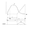
図5は、図2の液晶表示装置におけるディストーションモジュールで実行される発光輝度レベル選択処理の一例を説明するための図である。h1は映像信号のYヒストグラムを示している。ここで横軸は映像信号の入力階調(映像信号としてとりうる画素値、又は映像信号レベルともいう)を示し、縦軸は各映像信号レベルの頻度を示している。
<<
FIG. 5 is a diagram for explaining an example of the light emission luminance level selection process executed by the distortion module in the liquid crystal display device of FIG. h1 represents a Y histogram of the video signal. Here, the horizontal axis represents the input gradation of the video signal (also referred to as a pixel value or video signal level that can be taken as the video signal), and the vertical axis represents the frequency of each video signal level.
このような映像のヒストグラムh1に対して、使用する液晶パネルにおいてバックライトの発光輝度レベルが100%の時に表示可能な映像輝度範囲をAとする。また、ターゲットCRの液晶パネルで表示可能な映像輝度範囲をBとする。また、ディストーションモジュール5で選択可能な発光輝度レベルのうち、ある特定の発光輝度レベルで表示可能な映像輝度範囲をCとする。そして、ヒストグラムh1において、映像輝度範囲Cの両側で映像輝度範囲Bと重なる部分が、上述の数値化を行う対象となる部分であり、評価値算出部分である。この評価値算出部分のうち、低輝度部分をD1、高輝度部分をD2とする。
For such a video histogram h1, A is a video luminance range that can be displayed when the light emission luminance level of the backlight is 100% in the liquid crystal panel to be used. Also, let B be the video luminance range that can be displayed on the liquid crystal panel of the target CR. Also, let C be an image luminance range that can be displayed at a specific light emission luminance level among the light emission luminance levels that can be selected by the
評価値(Distortion)は、選択可能な発光輝度レベルに対して、頻度と重み付けによって下式(1)によって算出する。
Distortion=Σ{(映像輝度範囲D1+D2の頻度)×(距離重み)}・・・(1)
The evaluation value (Distortion) is calculated by the following equation (1) based on the frequency and weighting with respect to the selectable light emission luminance level.
Distortion = Σ {(frequency of image luminance range D1 + D2) × (distance weight)} (1)
重みとしては、評価値算出対象となる発光輝度レベルで表示可能な映像輝度範囲Cから遠ざかる程大きくする距離重みを用いる。ここでは、低輝度部分D1の距離重みをE1、高輝度部分D2の距離重みをE2とする。従って、同じ頻度値であっても、表現できる範囲から遠いほうが、評価値は大きくなる。これは表現できる範囲から遠いほうが、映像として表現できない影響が大きいためである。頻度と重み付けによって算出した値はF1(低輝度部分)、F2(高輝度部分)である。評価値はF1とF2の面積(累計)を合計した値となる。 As the weight, a distance weight that increases as the distance from the image luminance range C that can be displayed at the light emission luminance level that is an evaluation value calculation target increases. Here, the distance weight of the low luminance portion D1 is E1, and the distance weight of the high luminance portion D2 is E2. Therefore, even if the frequency value is the same, the evaluation value becomes larger as it is far from the range that can be expressed. This is because the farther from the range that can be expressed, the greater the influence that cannot be expressed as video. The values calculated by the frequency and the weight are F1 (low luminance part) and F2 (high luminance part). The evaluation value is the sum of the areas (cumulative total) of F1 and F2.
ディストーションモジュール5では、各発光輝度レベルに対して算出した評価値のうち、最も評価値が低い映像輝度範囲Cに対応する発光輝度レベルを、出力する発光輝度レベルBLreducedとして選択する。このとき、ディストーションモジュール5では、BL輝度レベル設定部8で設定され、第2のテンポラリフィルタ9によって緩和された発光輝度レベルBLrefを越えない範囲で、最も評価値が低い映像輝度範囲Cに対応する発光輝度レベルBLreducedを選択する。
The
このような評価値の算出は、ディストーションモジュール5で、選択可能な発光輝度レベルの全てについて行うことが理想である。しかし、処理時間等の制限があるため、選択可能な発光輝度レベルの輝度制御範囲を均等に分け、例えば10%程度毎の発光輝度レベルについて算出すればよい。
Ideally, the evaluation value is calculated for all selectable light emission luminance levels in the
つまり、上式(1)の特定の発光輝度レベルで表示可能な映像輝度範囲をCとして、選択可能な発光輝度レベルを順次適用し、発光輝度レベルごとに評価値を算出する。そして算出した評価値の中から、最も低い評価値をもつ発光輝度レベルを、選択した発光輝度レベルBLreducedとし、この値を第1のテンポラリフィルタ7に出力してバックライトの調光制御に用いるとともに、コンフィグレーションデザイン部13に出力して映像ゲインの設定(算出)に用いる。
That is, the video luminance range that can be displayed at the specific light emission luminance level of the above equation (1) is set as C, and the selectable light emission luminance levels are sequentially applied to calculate the evaluation value for each light emission luminance level. The light emission luminance level having the lowest evaluation value among the calculated evaluation values is set as the selected light emission luminance level BLreduced, and this value is output to the first temporary filter 7 to be used for backlight dimming control. And output to the
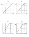
ディストーションモジュール5での選択処理を、図6〜図9を参照し具体的な数値で説明する。図6は、本発明に係る液晶表示装置における輝度変調処理の具体例を説明するための図で、映像ヒストグラムにおけるパネルCRとターゲットCRとの関係の一例を示す図である。ここでは、使用する液晶パネルのCR(パネルCR)が2000、ターゲットCRが3500、バックライトの輝度制御範囲が20〜100%で、バックライト輝度100%のときの液晶パネルの最大輝度は450cdとする。また、図6における各アルファベット記号は図5に準拠する。
The selection processing in the
この例において、使用する液晶パネルで表示可能な映像輝度範囲Aは、450cd〜0.225cdである。また、目標とする液晶パネルの表示可能な映像輝度範囲Bは、450cd〜0.128cdである。そして、各映像信号レベル0〜255に対する頻度を映像輝度範囲Bに合わせるように割り付ける。この場合、映像輝度範囲Aと映像輝度範囲Bとの差は5デジット程度である。
In this example, the video luminance range A that can be displayed on the liquid crystal panel to be used is 450 cd to 0.225 cd. In addition, the target image luminance range B that can be displayed on the liquid crystal panel is 450 cd to 0.128 cd. Then, the frequency for each
ヒストグラムh1において、映像輝度範囲Bと映像輝度範囲Aとの差の部分に映像があれば、バックライトの発光輝度レベルを下げることで、よりターゲットCRに近い輝度表現が可能になる。しかし、高輝度側にも映像が分布していると、バックライトの発光輝度レベルを下げることで表現できない部分が発生する。そこで、上述したように、評価値を算出して最適な発光輝度レベルBLreducedを求める。 If there is an image in the difference between the image luminance range B and the image luminance range A in the histogram h1, the luminance expression closer to the target CR can be expressed by lowering the light emission luminance level of the backlight. However, if an image is distributed on the high luminance side, a portion that cannot be expressed by reducing the light emission luminance level of the backlight occurs. Therefore, as described above, the evaluation value is calculated to obtain the optimum light emission luminance level BLreduced.
図7は、選択対象の一つである発光輝度レベル100%のときの映像輝度範囲Cを示す図、図8は、選択対象の一つである発光輝度レベル70%程度のときの映像輝度範囲Cを示す図、図9は、選択対象の一つである発光輝度レベル50%程度のときの映像輝度範囲Cを示す図である。図7〜図9における各アルファベット記号は図5に準拠する。 FIG. 7 is a diagram showing a video luminance range C when the light emission luminance level is 100%, which is one of the selection targets, and FIG. 8 is a video luminance range when the light emission luminance level is about 70%, which is one of the selection targets. FIG. 9 is a diagram showing a video luminance range C at a light emission luminance level of about 50%, which is one of the selection targets. Each alphabet symbol in FIGS. 7-9 is based on FIG.
図7で示したように、発光輝度レベルが100%を示すものである場合、低輝度部分の評価値F1には或る程度の値があり、高輝度部分の評価値F2には値がない。また、図8で示したように、発光輝度レベルを70%程度に下げた場合、低輝度部分の評価値F1及び高輝度部分の評価値F2ともに、低い値を持つ。また、図9で示したように、発光輝度レベルを50%程度に下げた場合、低輝度部分の評価値F1には値がなく、高輝度部分の評価値F2には大きな値を持つ。図7〜図9で例示した各発光輝度レベルでの評価値算出結果の面積(累積)を比較してみると、発光輝度レベルが70%のときが最も低い。従って、ディストーションモジュール5では発光輝度レベル70%を選択し、出力することになる。
As shown in FIG. 7, when the emission luminance level indicates 100%, the evaluation value F1 for the low luminance portion has a certain value, and the evaluation value F2 for the high luminance portion has no value. . Further, as shown in FIG. 8, when the emission luminance level is lowered to about 70%, both the low luminance portion evaluation value F1 and the high luminance portion evaluation value F2 have low values. As shown in FIG. 9, when the emission luminance level is lowered to about 50%, the evaluation value F1 for the low luminance portion has no value, and the evaluation value F2 for the high luminance portion has a large value. Comparing the areas (cumulative) of the evaluation value calculation results at the respective light emission luminance levels exemplified in FIGS. 7 to 9, the light emission luminance level is the lowest when it is 70%. Therefore, the
《コンフィグレーションデザイン部13》
液晶パネルへ入力される画素値と液晶パネルでの表示輝度との関係を示す基本的なモデルは、下式(2)により示される。ここで、Yは液晶パネルでの表示輝度、BLはバックライトの発光輝度レベル(バックライトDUTY)、CV(Code Value)は液晶パネルへ入力される画素値である。また、この例では映像信号の階調は0〜255で量子化されているものとする。
Y=BL(CV/255)γ ・・・(2)
<<
A basic model showing the relationship between the pixel value input to the liquid crystal panel and the display brightness on the liquid crystal panel is expressed by the following equation (2). Here, Y is the display luminance on the liquid crystal panel, BL is the light emission luminance level of the backlight (backlight DUTY), and CV (Code Value) is the pixel value input to the liquid crystal panel. In this example, it is assumed that the gradation of the video signal is quantized from 0 to 255.
Y = BL (CV / 255) γ (2)
コンフィグレーションデザイン部13は、ディストーションモジュール5で選択された発光輝度レベルBLreducedによってバックライトの発光輝度が低下したときに、画面上の輝度を上げるように、映像ゲインを調整する。ゲインをかけた画素値をCVreduced とするとき、発光輝度レベルを低下させたときの画面の明るさ(液晶パネルでの表示輝度)は、BLreduced(CVreduced/255)γである。一方で、参照用発光輝度レベルBLrefでバックライトを制御したときの画面の明るさは、BLref(CVref/255)γとなる。これらの値を等しくさせ、発光輝度レベルBLreducedによって生じるバックライトの発光輝度の低下分を補償するように、画素値を決定すればよい。つまり、コンフィグレーションデザイン部13は、下式(3)を満たすようなゲイン設定を行えばよい。
Y=BLreduced(CVreduced/255)γ=BLref(CVref/255)γ・・・(3)
The
Y = BLreduced (CVreduced / 255) γ = BLref (CVref / 255) γ (3)
従って、ゲイン(Gとする)は、下式(4)のようになる。例えば、参照用発光輝度レベルBLrefが100%のときには、下式(5)のようになる。なお、BLrefとBLreducedとの関係をルックアップテーブルとしてコンフィグレーションデザイン部13のROMなどに格納しておき、下式(4)の演算処理を高速に実行させることが好ましい。
Therefore, the gain (G) is expressed by the following equation (4). For example, when the reference light emission luminance level BLref is 100%, the following equation (5) is obtained. It is preferable to store the relationship between BLref and BLreduced as a look-up table in the ROM of the
G=CVreduced/CVref=(BLref/BLreduced)1/γ・・・(4)
G=(1/BLreduced)1/γ ・・・(5)
G = CVreduced / CVref = (BLref / BLreduced) 1 / γ (4)
G = (1 / BLreduced) 1 / γ (5)
図10は、図2の液晶表示装置におけるアドバンスト輝度変調部から出力されるゲイン設定信号に基づきRGBγ/WB調整部で設定される映像信号ゲインの例を示す図である。 FIG. 10 is a diagram illustrating an example of the video signal gain set by the RGBγ / WB adjustment unit based on the gain setting signal output from the advanced luminance modulation unit in the liquid crystal display device of FIG.
図10を参照して、入力されるゲイン設定値(変換係数)とそこから得るゲインカーブの関係について説明する。図10(A)に示すように、アドバンスト輝度変調部20から出力される映像信号のゲイン設定が1.0の場合には全輝度について線形のゲインカーブで問題ない。しかし、ゲインが1.0以上の場合、図10(B)に示すように、高輝度部分が一律255の値となり、いわゆる白つぶれが発生する。アドバンスト輝度変調処理では、例えば、少数の白輝度部分の白つぶれを犠牲にして、黒部分をより引き締めるようにゲイン設定してもよいが、白つぶれを起こす階調範囲が広い場合においては、表示品位を大きく低下させることになってしまう。
With reference to FIG. 10, the relationship between the input gain setting value (conversion coefficient) and the gain curve obtained therefrom will be described. As shown in FIG. 10A, when the gain setting of the video signal output from the advanced
そこで、低中輝度については、ゲイン設定に応じた信号伸張を行い、高輝度については、ゲインカーブを非線形にすることによって、高輝度部分の階調性の低下を軽減することが好ましい(白つぶれを防ぐこと)。この手法は明るさと白つぶれのトレードオフの関係になる。非線形とする領域を狭めれば、正規の明るさを表現できる領域が増えるが、高輝度の階調性が低下する。逆に、非線形とする領域を広めれば正規の明るさを表現できる領域が減るが、高輝度の階調性が或る程度保たれることになる。実際には非線形とする輝度は、ゲイン設定による出力の例えば90%以上の部分や95%以上の部分とするなどして、白つぶれの影響のある部分のみ非線形とすればよい。図10(C)には、ゲイン設定が1.2の場合に90%以上の部分を非線形にするように補正したゲインカーブを示している。また、図10(D)には、ゲイン設定が1.6の場合に90%以上の部分を非線形にするように補正したゲインカーブを示している。 Therefore, it is preferable to reduce the gradation of the high-brightness part by performing signal expansion according to the gain setting for low and medium brightness and making the gain curve non-linear for high brightness. To prevent). This method has a trade-off relationship between brightness and whiteout. If the non-linear region is narrowed, the region in which normal brightness can be expressed increases, but the high luminance gradation is lowered. Conversely, if the non-linear region is widened, the region where normal brightness can be expressed decreases, but the high luminance gradation is maintained to some extent. In practice, the non-linear luminance may be made non-linear only in the portion affected by the white-out, for example, by setting the output by the gain setting to 90% or more or 95% or more. FIG. 10C shows a gain curve corrected so that a portion of 90% or more becomes non-linear when the gain setting is 1.2. FIG. 10D shows a gain curve that is corrected so that a portion of 90% or more becomes non-linear when the gain setting is 1.6.
また、上述のように、ゲイン設定が1.0を超えた場合に生じる高輝度部分の白つぶれを避けるためには、ゲインカーブの高階調領域を一部非線形にする必要がある。しかし、RGBγ/WB調整部15は、ゲイン設定に基づき単純に比例計算を行うため、このようなゲインカーブを算出ことができない。そのため、ゲイン設定ごとにゲインカーブをメモリに格納するようにしてもよいし、もしくは、ゲインカーブの線形部分はゲイン設定値から単純に比例計算し、図10(C),(D)に例示したように90%以上の部分については、補間等によって非線形部分を算出するようにしてもよい。なお、ゲイン設定はバックライトの輝度変化に応じて、フレームごとにゲインカーブが算出される場合もあれば、複数のフレーム単位で算出される場合もある。
Further, as described above, in order to avoid whiteout in a high luminance portion that occurs when the gain setting exceeds 1.0, it is necessary to make the high gradation region of the gain curve partly non-linear. However, since the RGBγ /
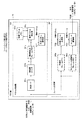
図11は、本発明の液晶表示装置が備える動き補償型FRC部の構成例を示すブロック図である。このFRC部16は、大きく分けて、入力映像信号に含まれる2つの連続したフレーム間で動きベクトルを検出するベクトル検出部161と、検出した動きベクトルに基づいて内挿フレーム(内挿映像)を生成するフレーム生成部162とで構成される。なお、ベクトル検出部161は、動きベクトル検出に反復勾配法を用いた場合の例について示すが、この反復勾配法に限定されず、ブロックマッチング法などを用いてもよい。
FIG. 11 is a block diagram illustrating a configuration example of a motion compensation type FRC unit included in the liquid crystal display device of the present invention. The
ここで、反復勾配法の特徴は、動きベクトルの検出がブロック単位で可能であるため、数種類の動き量が検出でき、また、小領域の動物体でも動きベクトルを検出することができる。また、回路構成も他の方式(ブロックマッチング法など)と比較して小規模で実現することができる。この反復勾配法では、被検出ブロックに対して、すでに検出された近傍のブロックの動きベクトルを初期偏位ベクトルとして、これを起点として勾配法の演算を繰り返す方法が用いられる。この方法によれば、勾配法の繰り返しは2回程度でほぼ正確な動き量を得ることができる。 Here, the feature of the iterative gradient method is that a motion vector can be detected in units of blocks, so that several types of motion amounts can be detected, and a motion vector can be detected even in a small-sized moving object. Also, the circuit configuration can be realized on a small scale as compared with other methods (block matching method or the like). In this iterative gradient method, a method is used in which the gradient method is repeated for the detected block, using the motion vector of a nearby block that has already been detected as an initial displacement vector, and starting from this. According to this method, it is possible to obtain an almost accurate motion amount by repeating the gradient method about twice.
図11において、ベクトル検出部161は、入力映像信号(RGB信号)から輝度信号(Y信号)を抽出する輝度信号抽出部161aと、抽出したY信号にLPFを掛けて高域部の帯域を制限するための前処理フィルタ161bと、動き検出用フレームメモリ161cと、初期ベクトル候補を蓄積するための初期ベクトルメモリ161dと、反復勾配法を用いてフレーム間の動きベクトルを検出する動きベクトル検出部161eと、検出した動きベクトルに基づいてフレーム間に内挿ベクトルを割り付ける内挿ベクトル評価部161fとを備える。
なお、動きベクトル検出部11eは本発明の動きベクトル検出部に相当し、内挿ベクトル評価部11fは本発明の内挿ベクトル割付部に相当する。
In FIG. 11, a
The motion vector detection unit 11e corresponds to the motion vector detection unit of the present invention, and the interpolation vector evaluation unit 11f corresponds to the interpolation vector allocation unit of the present invention.
上記反復勾配法の演算は画素の微分成分を用いているため、ノイズの影響を受け易く、また、検出ブロック内の勾配の変化量が多いと演算誤差が大きくなるため、前処理フィルタ161bにおいてLPFをかけて高域部の帯域を制限しておく。初期ベクトルメモリ161dには、初期ベクトル候補として、前々フレームで既に検出されている動きベクトル(初期ベクトル候補)を蓄積しておく。 Since the calculation of the iterative gradient method uses the differential component of the pixel, it is easily affected by noise, and the calculation error increases if the gradient change amount in the detection block is large. To limit the high-frequency band. In the initial vector memory 161d, motion vectors (initial vector candidates) already detected in the previous frame are stored as initial vector candidates.
動きベクトル検出部161eは、初期ベクトルメモリ161dに蓄積されている初期ベクトル候補の中から被検出ブロックの動きベクトルに最も近い動きベクトルを初期ベクトルとして選択する。すなわち、被検出ブロック近傍のブロックにおける既検出動きベクトル(初期ベクトル候補)の中からブロックマッチング法により初期ベクトルを選択する。そして、動きベクトル検出部161eは、選択した初期ベクトルを起点として、勾配法演算によって前フレームと現フレーム間の動きベクトルを検出する。
The motion
内挿ベクトル評価部161fは、動きベクトル検出部161eにより検出された動きベクトルを評価し、その評価結果に基づいて最適な内挿ベクトルをフレーム間の内挿ブロックに割り付けて、フレーム生成部162に出力する。
The interpolation vector evaluation unit 161f evaluates the motion vector detected by the motion
フレーム生成部162は、2つの入力フレーム(前フレーム、現フレーム)を蓄積するための内挿用フレームメモリ162aと、内挿用フレームメモリ162aからの2つの入力フレームと内挿ベクトル評価部161fからの内挿ベクトルとに基づいて内挿フレームを生成する内挿フレーム生成部162bと、入力フレーム(前フレーム、現フレーム)を蓄積するためのタイムベース変換用フレームメモリ162cと、タイムベース変換用フレームメモリ162cからの入力フレームに内挿フレーム生成部162bからの内挿フレームを挿入するタイムベース変換部162dと、を備えて構成される。
なお、内挿フレーム生成部162bは本発明の内挿映像生成部に相当し、タイムベース変換部162dは本発明の映像内挿部に相当する。
The
The interpolation frame generation unit 162b corresponds to the interpolation video generation unit of the present invention, and the time
図12は、フレーム生成部162による内挿フレーム生成処理の一例を説明するための図である。内挿フレーム生成部162bは、内挿ブロックに割り付けられた内挿ベクトルVを前フレーム、現フレームに伸ばして、各フレームとの交点近傍の画素を用いて内挿ブロック内の各画素を補間する。例えば、前フレームでは近傍3点よりA点の輝度を算出する。現フレームでは近傍3点よりB点の輝度を算出する。内挿フレームではP点の輝度をA点とB点の輝度から補間する。P点の輝度は、例えばA点の輝度とB点の輝度の平均としてもよい。
FIG. 12 is a diagram for explaining an example of the interpolation frame generation process by the
上記のようにして生成された内挿フレームは、タイムベース変換部162dに送られる。タイムベース変換部162dは、前フレーム、現フレームの間に、内挿フレームを挟み込んで、フレームレートを変換する処理を行う。このように、FRC部16により、入力映像信号(60フレーム/秒)を、動き補償された出力映像信号(120フレーム/秒)へ変換でき、これを表示パネルに出力することにより、動きぼけを低減して動画質を改善することが可能となる。なお、ここでは、60フレーム/秒の入力映像信号を、120フレーム/秒の出力映像信号にフレームレート変換する場合について説明するが、例えば90フレーム/秒、180フレーム/秒の出力映像信号を得る場合に適用しても良いことは言うまでもない。
The interpolated frame generated as described above is sent to the time
本発明に係る映像表示装置の主たる特徴部分は、動き補償型のFRC処理を行う際に、シーンチェンジを精度良く判定し、適切なFRC処理を行えるようにすることである。このための構成として、入力映像信号のヒストグラムに基づいてシーンチェンジか否かを検出するシーンチェンジ検出手段に相当するシーンチェンジ検出部6と、入力映像信号のフレーム間に、動き補償処理を施した映像信号を内挿することにより、入力映像信号のフレーム数を変換して表示パネル(図示せず)へ出力するレート変換手段に相当するFRC部16とを備える。FRC部16は、シーンチェンジ検出部6によりシーンチェンジが検出された場合に、動きベクトルを初期化する。
The main characteristic part of the video display device according to the present invention is to accurately determine a scene change and perform an appropriate FRC process when performing a motion compensation type FRC process. As a configuration for this, a motion compensation process is performed between a scene
図11において、シーンチェンジ検出部6からシーンチェンジ検出信号が出力され、FRC部16に入力された場合、動きベクトル検出部161eが動きベクトルを初期化、すなわち、初期ベクトルメモリ161dに蓄積されている初期ベクトル候補を初期化する。初期ベクトルメモリ161dには初期ベクトル候補として、前々フレームで既に検出されている動きベクトルが蓄積されているが、動きベクトル検出部161eによる動きベクトルの初期化に伴い、これらの初期ベクトル候補がリセットされ、シーンチェンジ後のフレーム間で動きベクトルを検出して初期ベクトル候補を初期ベクトルメモリ161dに蓄積し直す。
In FIG. 11, when a scene change detection signal is output from the scene
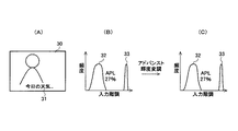
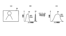
図13は、字幕が有る場合のアドバンスト輝度変調後のヒストグラムとAPLの変化例について説明するための図である。また、図14は、字幕が無い場合のアドバンスト輝度変調後のヒストグラムとAPLの変化例について説明するための図である。図中、30は映像フレーム、31は字幕、32は映像フレーム30のヒストグラム、33は字幕31のヒストグラム、34は輝度変調処理後のヒストグラムを示す。ここでは、字幕有りの映像と字幕無しの同じような映像とが連続して入力された場合について説明する。
FIG. 13 is a diagram for explaining an example of changes in the histogram and APL after advanced luminance modulation when there is a caption. FIG. 14 is a diagram for explaining an example of changes in the histogram and APL after advanced luminance modulation when there is no caption. In the figure, 30 is a video frame, 31 is a caption, 32 is a histogram of the
図13(A)に示す映像フレーム30は字幕31を含んでおり、図13(B)に示すようなヒストグラムがシーンチェンジ検出部6に入力される。なお、このときのAPLは27%とする。この映像フレーム30に対して、アドバンスト輝度変調処理を行った場合、映像フレーム30は字幕31の白ピークを含み、その映像信号は0から255の値を持つために、輝度変調処理後の映像信号は図13(C)に示すように0から255の値でゲインを変化させることはない。この場合APLも当然変化せず27%となる。
A
一方、次のフレームとして、図14(A)に示す映像フレーム30が入力された場合、この映像フレーム30は字幕を含まないため、図14(B)に示すようなヒストグラムがシーンチェンジ検出部6に入力される。なお、このときのAPLは25%とする。この映像フレーム30に対して、アドバンスト輝度変調処理を行った場合、映像フレーム30は字幕等の白ピークがない暗い映像であるため、図14(C)に示すように、輝度変調処理によりゲインを変化させダイナミックレンジ(例えば、0〜255)をフルに使用するように制御される。この場合APLは大きく変化して50%となる。
On the other hand, when the
上記の図13及び図14の例において、APLの変化に基づいて動きベクトルを初期化する従来例の場合、輝度変調処理後のAPLが図13(C)の27%から図14(C)の50%に変化しているため、同じようなシーンであるにも係らず、FRC部16ではシーンチェンジと判定してしまい、動きベクトルを初期化していた。
13 and 14, in the case of the conventional example in which the motion vector is initialized based on the change in APL, the APL after the luminance modulation processing is changed from 27% in FIG. 13C to that in FIG. Since it has changed to 50%, the
すなわち、輝度変調処理と共に、FRC処理を行う構成とした場合、同じようなシーンであっても、白ピークの有無によりAPLが大きく変化してしまうため、液晶表示装置はこのAPLの変化に基づいてシーンチェンジ有りと判定し、FRC処理時に動きベクトルを初期化してしまっていた。 In other words, when the FRC process is performed together with the luminance modulation process, the APL changes greatly depending on the presence or absence of the white peak even in the same scene, so the liquid crystal display device is based on the change of the APL. It was determined that there was a scene change, and the motion vector was initialized during FRC processing.
これに対して、ヒストグラムの変化に基づいて動きベクトルを初期化する本発明の場合、シーンチェンジ検出部6に入力されるヒストグラムが図13(B)から図14(B)に変化するため、ヒストグラムの変化量は図14(B)の斜線で示す部分(すなわち、字幕31のヒストグラム33)に相当することになる。このヒストグラムの変化量は所定値よりも小さいため、シーンチェンジ検出部6はシーンチェンジと判定せず、シーンチェンジ検出信号を出力しない。このため、FRC部16が動きベクトルを不必要に初期化することはない。
On the other hand, in the case of the present invention in which the motion vector is initialized based on the change of the histogram, the histogram input to the scene
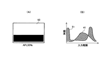
図15は、映像におけるAPLとヒストグラムとの関係の一例を示す図である。また、図16は、映像におけるAPLとヒストグラムとの関係の他の例を示す図である。図中、40は一般風景の映像フレーム、41は映像フレーム40のヒストグラム、50は白黒ブロックの映像フレーム50、51は映像フレーム50のヒストグラムを示す。ここでは、APLが同じで且つシーンが変化した映像が連続して入力された場合について説明する。
FIG. 15 is a diagram illustrating an example of the relationship between the APL and the histogram in the video. FIG. 16 is a diagram illustrating another example of the relationship between the APL and the histogram in the video. In the figure, 40 is a video frame of a general landscape, 41 is a histogram of the
シーンチェンジを検出する手段として、APLを用いた場合、図15(A)の一般風景から図16(A)の白黒ブロックのように、シーンが変化しても、たまたまAPLが同一(本例では50%)であると、液晶表示装置ではシーンチェンジがなかったものと判定してしまい、動きベクトルを初期化せず、画質を劣化させていた。 When APL is used as means for detecting a scene change, the APL happens to be the same (in this example, even if the scene changes from the general landscape in FIG. 15A to the black and white block in FIG. 16A). 50%), it was determined that there was no scene change in the liquid crystal display device, the motion vector was not initialized, and the image quality was deteriorated.
これに対して、ヒストグラムの変化に基づいて動きベクトルを初期化する本発明の場合、シーンチェンジ検出部6に入力されるヒストグラムが図15(B)から図16(B)に変化するため、ヒストグラムの変化量は図16(B)の斜線で示す部分に相当することになる。このヒストグラムの変化量は所定値よりも大きいため、シーンチェンジ検出部6はシーンチェンジと判定し、シーンチェンジ検出信号を出力する。このため、FRC部16が動きベクトルを適切に初期化することができる。
On the other hand, in the case of the present invention in which the motion vector is initialized based on the change in the histogram, the histogram input to the scene
なお、上記の所定値は、予め様々なコンテンツのヒストグラムの変化量に対して、FRC処理を初期化するか否かに応じた画質の劣化具合を分析することにより決定すればよい。すなわち、シーンチェンジと判定せずにFRC処理を継続させるよりも、シーンチェンジと判定してFRC処理を初期化させたほうが画質の劣化が小さくなるように所定値を決定すればよい。 The predetermined value may be determined in advance by analyzing the degree of image quality deterioration according to whether or not to initialize the FRC process with respect to the amount of change in the histogram of various contents. That is, rather than continuing the FRC process without determining the scene change, the predetermined value may be determined so that the image quality degradation is smaller when the FRC process is determined and the FRC process is initialized.
上記より、ヒストグラムによるシーンチェンジ検出は、APLの場合よりも精度が高いことがわかる。図15及び図16に示した例のように、APLではシーン変化をうまく検出できない場合であっても、ヒストグラムによりシーン変化を精度良く検出することができる。 From the above, it can be seen that the scene change detection by the histogram is more accurate than in the case of APL. As in the example shown in FIGS. 15 and 16, even if the scene change cannot be detected well by the APL, the scene change can be detected accurately by the histogram.
ここで、アドバンスト輝度変調処理を行うためには映像内の輝度分布を知る必要があり、このため最も合理的と考えられるヒストグラムが用いられている。そして、ヒストグラムの2次的な利用として、シーンチェンジの検出に用いることができ、さらに、FRC処理時に動きベクトルの初期化を行うか否かの判定基準として用いることができる。 Here, in order to perform the advanced luminance modulation process, it is necessary to know the luminance distribution in the video, and for this reason, the most reasonable histogram is used. As a secondary use of the histogram, it can be used to detect a scene change, and can be used as a criterion for determining whether or not to initialize a motion vector during FRC processing.
このように、動き補償型のFRC処理を行う際に、入力映像信号のヒストグラムに基づいてシーンチェンジを精度良く判定することができるため、適切なFRC処理を行うことができる。 As described above, when the motion compensation type FRC process is performed, the scene change can be accurately determined based on the histogram of the input video signal, so that the appropriate FRC process can be performed.
1…スケーリング部、2…Yヒストグラム検出部、3…APL検出部、4…ヒストグラムストレッチング部、5…ディストーションモジュール、6…シーンチェンジ検出部、7…第1のテンポラリフィルタ、8…BL輝度レベル設定部、9…第2のテンポラリフィルタ、10…可変ディレイ、11…CPU/CPLD、12…BL調整部、13…コンフィグレーションデザイン部、14…画質補正部、15…RGBγ/WB調整部、16…FRC部、17…映像出力部、20…アドバンスト輝度変調部、161…ヒストグラムバッファ、162…ヒストグラム変化検出部、161…ベクトル検出部、161a…輝度信号抽出部、161b…前処理フィルタ、161c…動き検出用フレームメモリ、161d…初期ベクトルメモリ、161e…動きベクトル検出部、161f…内挿ベクトル評価部、162…フレーム生成部、162a…内挿用フレームメモリ、162b…内挿フレーム生成部、162c…タイムベース変換用フレームメモリ、162d…タイムベース変換部。 DESCRIPTION OF SYMBOLS 1 ... Scaling part, 2 ... Y histogram detection part, 3 ... APL detection part, 4 ... Histogram stretching part, 5 ... Distortion module, 6 ... Scene change detection part, 7 ... 1st temporary filter, 8 ... BL brightness level Setting unit, 9 ... second temporary filter, 10 ... variable delay, 11 ... CPU / CPLD, 12 ... BL adjustment unit, 13 ... configuration design unit, 14 ... image quality correction unit, 15 ... RGB γ / WB adjustment unit, 16 DESCRIPTION OF SYMBOLS ... FRC part, 17 ... Video output part, 20 ... Advanced luminance modulation part, 161 ... Histogram buffer, 162 ... Histogram change detection part, 161 ... Vector detection part, 161a ... Luminance signal extraction part, 161b ... Preprocessing filter, 161c ... Frame memory for motion detection, 161d ... initial vector memory, 161e ... Vector detection unit, 161f ... interpolation vector evaluation unit, 162 ... frame generation unit, 162a ... frame memory for interpolation, 162b ... frame generation unit for interpolation, 162c ... frame memory for time base conversion, 162d ... time base conversion unit .
Claims (4)
前記入力映像信号のヒストグラムに基づいてシーンチェンジか否かを検出するシーンチェンジ検出手段を備え、
前記レート変換手段は、前記シーンチェンジ検出手段によりシーンチェンジが検出された場合に、動きベクトルを初期化することを特徴とする映像表示装置。 Rate conversion means for converting the number of frames or fields of the input video signal and outputting it to the display panel by interpolating the video signal subjected to motion compensation between frames or fields of the input video signal A video display device,
Scene change detection means for detecting whether or not a scene change based on a histogram of the input video signal;
The video display device, wherein the rate conversion means initializes a motion vector when a scene change is detected by the scene change detection means.
Priority Applications (1)
| Application Number | Priority Date | Filing Date | Title |
|---|---|---|---|
| JP2008165474A JP5139897B2 (en) | 2008-06-25 | 2008-06-25 | Video display device |
Applications Claiming Priority (1)
| Application Number | Priority Date | Filing Date | Title |
|---|---|---|---|
| JP2008165474A JP5139897B2 (en) | 2008-06-25 | 2008-06-25 | Video display device |
Publications (2)
| Publication Number | Publication Date |
|---|---|
| JP2010008535A true JP2010008535A (en) | 2010-01-14 |
| JP5139897B2 JP5139897B2 (en) | 2013-02-06 |
Family
ID=41589162
Family Applications (1)
| Application Number | Title | Priority Date | Filing Date |
|---|---|---|---|
| JP2008165474A Expired - Fee Related JP5139897B2 (en) | 2008-06-25 | 2008-06-25 | Video display device |
Country Status (1)
| Country | Link |
|---|---|
| JP (1) | JP5139897B2 (en) |
Cited By (2)
| Publication number | Priority date | Publication date | Assignee | Title |
|---|---|---|---|---|
| WO2013015217A1 (en) * | 2011-07-25 | 2013-01-31 | シャープ株式会社 | Stereoscopic image processing device and stereoscopic image processing method |
| JP7334608B2 (en) | 2019-12-19 | 2023-08-29 | 株式会社Jvcケンウッド | VIDEO SIGNAL PROCESSING DEVICE AND VIDEO SIGNAL PROCESSING METHOD |
Citations (5)
| Publication number | Priority date | Publication date | Assignee | Title |
|---|---|---|---|---|
| JP2000333134A (en) * | 1999-05-20 | 2000-11-30 | Toshiba Corp | Interpolation field generating circuit and field double speed conversion circuit |
| JP2006121274A (en) * | 2004-10-20 | 2006-05-11 | Victor Co Of Japan Ltd | Scene change detecting device |
| JP2006352611A (en) * | 2005-06-17 | 2006-12-28 | Hitachi Displays Ltd | Picture interpolator, frame rate changer and picture display |
| JP2008076755A (en) * | 2006-09-21 | 2008-04-03 | Toshiba Corp | Image display device and image display method |
| JP2008109627A (en) * | 2006-09-28 | 2008-05-08 | Sharp Corp | Image display apparatus and method, image processor, and method |
-
2008
- 2008-06-25 JP JP2008165474A patent/JP5139897B2/en not_active Expired - Fee Related
Patent Citations (5)
| Publication number | Priority date | Publication date | Assignee | Title |
|---|---|---|---|---|
| JP2000333134A (en) * | 1999-05-20 | 2000-11-30 | Toshiba Corp | Interpolation field generating circuit and field double speed conversion circuit |
| JP2006121274A (en) * | 2004-10-20 | 2006-05-11 | Victor Co Of Japan Ltd | Scene change detecting device |
| JP2006352611A (en) * | 2005-06-17 | 2006-12-28 | Hitachi Displays Ltd | Picture interpolator, frame rate changer and picture display |
| JP2008076755A (en) * | 2006-09-21 | 2008-04-03 | Toshiba Corp | Image display device and image display method |
| JP2008109627A (en) * | 2006-09-28 | 2008-05-08 | Sharp Corp | Image display apparatus and method, image processor, and method |
Cited By (3)
| Publication number | Priority date | Publication date | Assignee | Title |
|---|---|---|---|---|
| WO2013015217A1 (en) * | 2011-07-25 | 2013-01-31 | シャープ株式会社 | Stereoscopic image processing device and stereoscopic image processing method |
| JP2013026943A (en) * | 2011-07-25 | 2013-02-04 | Sharp Corp | Stereoscopic image processing apparatus and stereoscopic image processing method |
| JP7334608B2 (en) | 2019-12-19 | 2023-08-29 | 株式会社Jvcケンウッド | VIDEO SIGNAL PROCESSING DEVICE AND VIDEO SIGNAL PROCESSING METHOD |
Also Published As
| Publication number | Publication date |
|---|---|
| JP5139897B2 (en) | 2013-02-06 |
Similar Documents
| Publication | Publication Date | Title |
|---|---|---|
| JP5091955B2 (en) | Video display device | |
| JP5091701B2 (en) | Liquid crystal display | |
| JP3430998B2 (en) | Image display device and image display method | |
| JP4203090B2 (en) | Image display device and image display method | |
| JP4231071B2 (en) | Image display device, image display method, and image display program | |
| JP5338019B2 (en) | Image display device | |
| JP2010085524A (en) | Liquid crystal display | |
| JP5197858B1 (en) | Video display device and television receiver | |
| JP2009205128A (en) | Display device | |
| JP2013161018A (en) | Video display device and television receiver | |
| JP2009098574A (en) | Image processing apparatus, image display device and image processing method | |
| JP5039566B2 (en) | Method and apparatus for improving visual perception of image displayed on liquid crystal screen, liquid crystal panel, and liquid crystal screen | |
| JP2004326082A (en) | Display controller and display device | |
| US8958657B2 (en) | Frame rate conversion image processing apparatus, control method, and computer-readable storage medium | |
| JP2004326082A5 (en) | ||
| JP2010271480A (en) | Display device | |
| JP5236622B2 (en) | Display device | |
| JP5070114B2 (en) | Video display device | |
| JP5139897B2 (en) | Video display device | |
| JP5249703B2 (en) | Display device | |
| JP2011228926A (en) | Image signal processing apparatus and image display apparatus | |
| JP2009265114A (en) | Liquid crystal display device | |
| JP5091699B2 (en) | Video display device | |
| JP2011128182A (en) | Display device | |
| JP2008259097A (en) | Video signal processing circuit and video display device |
Legal Events
| Date | Code | Title | Description |
|---|---|---|---|
| A621 | Written request for application examination |
Free format text: JAPANESE INTERMEDIATE CODE: A621 Effective date: 20100826 |
|
| A131 | Notification of reasons for refusal |
Free format text: JAPANESE INTERMEDIATE CODE: A131 Effective date: 20120710 |
|
| A521 | Written amendment |
Free format text: JAPANESE INTERMEDIATE CODE: A523 Effective date: 20120904 |
|
| TRDD | Decision of grant or rejection written | ||
| A01 | Written decision to grant a patent or to grant a registration (utility model) |
Free format text: JAPANESE INTERMEDIATE CODE: A01 Effective date: 20121023 |
|
| A01 | Written decision to grant a patent or to grant a registration (utility model) |
Free format text: JAPANESE INTERMEDIATE CODE: A01 |
|
| A61 | First payment of annual fees (during grant procedure) |
Free format text: JAPANESE INTERMEDIATE CODE: A61 Effective date: 20121116 |
|
| R150 | Certificate of patent or registration of utility model |
Ref document number: 5139897 Country of ref document: JP Free format text: JAPANESE INTERMEDIATE CODE: R150 Free format text: JAPANESE INTERMEDIATE CODE: R150 |
|
| FPAY | Renewal fee payment (event date is renewal date of database) |
Free format text: PAYMENT UNTIL: 20151122 Year of fee payment: 3 |
|
| LAPS | Cancellation because of no payment of annual fees |