JP2010008437A - Electro-optical device, manufacturing method thereof, and electronic apparatus - Google Patents
Electro-optical device, manufacturing method thereof, and electronic apparatus Download PDFInfo
- Publication number
- JP2010008437A JP2010008437A JP2008157951A JP2008157951A JP2010008437A JP 2010008437 A JP2010008437 A JP 2010008437A JP 2008157951 A JP2008157951 A JP 2008157951A JP 2008157951 A JP2008157951 A JP 2008157951A JP 2010008437 A JP2010008437 A JP 2010008437A
- Authority
- JP
- Japan
- Prior art keywords
- electro
- substrates
- pair
- pixel
- shielding film
- Prior art date
- Legal status (The legal status is an assumption and is not a legal conclusion. Google has not performed a legal analysis and makes no representation as to the accuracy of the status listed.)
- Granted
Links
Images


Abstract
Description
本発明は、例えば単板式にてカラー表示可能である、液晶装置等の電気光学装置及びその製造方法、並びに電気光学装置を備えた、例えば携帯電話等の電子機器の技術分野に関する。 The present invention relates to an electro-optical device such as a liquid crystal device capable of color display, for example, in a single plate type, a manufacturing method thereof, and a technical field of an electronic apparatus such as a mobile phone including the electro-optical device.
この種の電気光学装置の一例である単板式の液晶装置では、一つの画素はRGB(即ち、赤色、緑色、青色)別の三つのサブ画素から構成されており、隣接する画素に異なる電位を供給することでカラー画像を表示している。 In a single-plate type liquid crystal device which is an example of this type of electro-optical device, one pixel is composed of three sub-pixels for RGB (that is, red, green, and blue), and different potentials are applied to adjacent pixels. The color image is displayed by supplying.
ここで、液晶を挟持する一対の基板間に、画像信号に応じて生じる電界(以下単に「縦電界」という)によって液晶を駆動する縦電界駆動方式の場合、高精細化という一般的要請下で、このようなサブ画素のピッチを小さくすると、相異なる電位の画像信号が供給される相隣接する画素電極間の電位差(以下単に「横電界」という)が、縦電界に対して相対的に大きくなってしまう。よって、横電界の悪影響が顕在化し、液晶の配向不良が問題となる。特に反転駆動方式で相隣接する画素電極間に極性の異なる電位の画像信号が供給される場合には、この問題は顕著となる。このため、画素電極の形状を、液晶の配向状態に応じて変形することにより、横電界を抑制するという技術が提案されている(特許文献1参照)。 Here, in the case of a vertical electric field driving method in which a liquid crystal is driven by an electric field generated in accordance with an image signal (hereinafter simply referred to as “longitudinal electric field”) between a pair of substrates sandwiching the liquid crystal, under the general demand for high definition. When the pitch of such subpixels is reduced, the potential difference between adjacent pixel electrodes to which image signals having different potentials are supplied (hereinafter simply referred to as “lateral electric field”) is relatively large with respect to the vertical electric field. turn into. Therefore, the adverse effect of the transverse electric field becomes obvious, and the alignment failure of the liquid crystal becomes a problem. This problem is particularly noticeable when image signals having different polarities are supplied between adjacent pixel electrodes by the inversion driving method. For this reason, a technique for suppressing the lateral electric field by changing the shape of the pixel electrode in accordance with the alignment state of the liquid crystal has been proposed (see Patent Document 1).
本願発明者の知るところでは、上述の背景技術によれば、ある特定の種類の電気光学物質を使用した電気光学装置については、画素電極を変えることによって横電界の発生を大なり小なりに抑制できる可能性がある。 The inventor of the present application knows that according to the background art described above, for an electro-optical device using a specific type of electro-optical material, the generation of a lateral electric field is suppressed to a greater or lesser extent by changing the pixel electrode. There is a possibility.
しかしながら、背景技術によれば、電圧無印加時における液晶の配向状態に基づいて画素電極の形状を決定する必要があるため、使用する液晶の種類によっては、画素電極の形状が複雑になってしまうという問題点がある。特に高精細化の要請の下で画素ピッチを小さくした液晶装置においては、複雑な形状を有する画素電極を画像表示領域全体に渡って均一に形成することは、技術的な困難性を伴う。特に単板式でカラー表示を行う液晶装置の場合、その性質上、画素ピッチを小さくする必要があるので、この問題は深刻さを増す。 However, according to the background art, since it is necessary to determine the shape of the pixel electrode based on the alignment state of the liquid crystal when no voltage is applied, the shape of the pixel electrode becomes complicated depending on the type of liquid crystal used. There is a problem. In particular, in a liquid crystal device in which the pixel pitch is reduced under the demand for higher definition, it is technically difficult to uniformly form pixel electrodes having a complicated shape over the entire image display region. In particular, in the case of a liquid crystal device that performs color display with a single plate type, this problem becomes serious because the pixel pitch needs to be reduced due to its nature.
本発明は、例えば上記問題点に鑑みてなされたものであり、単板式で高品位のカラー表示を行うことが可能であり、しかも高精細化に適している電気光学装置及びその製造方法、並びにそのような電気光学装置を備える電子機器を提供することを課題とする。 The present invention has been made, for example, in view of the above-described problems, and is capable of performing high-quality color display with a single plate type, and is suitable for high definition, and a manufacturing method thereof, and It is an object to provide an electronic apparatus including such an electro-optical device.
本発明の第1電気光学装置は上記課題を解決するために、一対の基板と、該一対の基板間に挟持された電気光学物質と、前記一対の基板の一方に、相交差するように配線された複数の走査線及び複数のデータ線と、前記一対の基板の一方における前記電気光学物質に面する側に、前記複数のデータ線及び前記複数の走査線の交差に対応する画素毎に配列された複数の画素電極と、前記一対の基板の他方に、前記複数の画素電極に前記電気光学物質を介して対向するように配置された対向電極と、前記一対の基板の少なくとも一方に設けられ、前記一対の基板上で平面的に見て、前記画素の開口領域を少なくとも部分的に規定する遮光膜とを備え、前記画素電極及び前記遮光膜は、前記一対の基板上で平面的に見て、前記画素電極及び前記遮光膜が部分的に重畳するように、配置されており、前記一対の基板間における基板間ギャップ距離X、並びに前記画素電極及び前記遮光膜が部分的に重畳する重畳幅Yは、不等式
Y≧0.625X−y
但し
y=−0.0208Δε2+0.5625Δε−3.0417
Δε=前記電気光学物質の誘電率異方性
を満たす。
In order to solve the above problems, a first electro-optical device according to the present invention has a pair of substrates, an electro-optical material sandwiched between the pair of substrates, and a wiring that crosses one of the pair of substrates. A plurality of scanning lines and a plurality of data lines arranged on a side facing the electro-optical material in one of the pair of substrates for each pixel corresponding to an intersection of the plurality of data lines and the plurality of scanning lines. Provided on at least one of the plurality of pixel electrodes, the other electrode of the pair of substrates, the counter electrode disposed to face the plurality of pixel electrodes via the electro-optic material, and the pair of substrates. A light shielding film that at least partially defines an opening region of the pixel when viewed in plan on the pair of substrates, and the pixel electrode and the light shielding film are viewed in plan on the pair of substrates. The pixel electrode and the light shielding Superimposing width Y is inequality but so as to overlap partially, are disposed, the pair of substrates gap distance X between substrates, and wherein the pixel electrode and the light-shielding film overlaps partially
Y ≧ 0.625X−y
However, y = −0.0208Δε 2 + 0.5625Δε−3.0417
Δε = the dielectric anisotropy of the electro-optic material is satisfied.
本発明の第1電気光学装置によれば、その動作時には、例えば電源信号、データ信号、制御信号等の各種信号が入出力されると、基板上に作り込まれた内蔵駆動回路又は外付けされた駆動回路によって、走査信号が第1方向(即ち、典型的には横方向又はX方向)に沿って形成された複数の走査線に対して順次供給される。これと並行して画像信号が第2方向(即ち、典型的には縦方向又はY方向)に沿って形成された複数のデータ線に対して、RGB(即ち赤色、緑色及び青色)別の画像信号が同時に又は逐次に供給される。その結果、画素毎に形成された画素電極と、対向する基板上に形成された対向電極間に生じる縦電界によって、基板間に挟持された電気光学物質の配向状態を変え、各画素における光透過率を制御することが可能となる。このように電気光学物質の配向状態を制御することによって、第1電気光学装置において、例えば液晶表示等の電気光学動作が、縦電界駆動によるアクティブマトリクス方式で行われる。 According to the first electro-optical device of the present invention, when various signals such as a power signal, a data signal, and a control signal are input and output during operation, the built-in drive circuit built on the substrate or externally attached. By the driving circuit, the scanning signal is sequentially supplied to a plurality of scanning lines formed along the first direction (that is, typically the horizontal direction or the X direction). In parallel with this, RGB (that is, red, green, and blue) separate images for a plurality of data lines in which the image signal is formed along the second direction (that is, typically the vertical direction or the Y direction). Signals are supplied simultaneously or sequentially. As a result, the vertical electric field generated between the pixel electrode formed for each pixel and the counter electrode formed on the opposing substrate changes the orientation state of the electro-optic material sandwiched between the substrates, and transmits light in each pixel. The rate can be controlled. By controlling the orientation state of the electro-optic material in this way, in the first electro-optic device, for example, an electro-optic operation such as a liquid crystal display is performed by an active matrix method using vertical electric field driving.
基板上には、開口領域となる画素の占める領域を規定するように遮光膜が形成され、画素電極が各画素に対応するように配置されている。各画素電極は、対応する開口領域の面積よりも大きく形成されている。そのため、基板上から平面的にみると、当該画素電極は、開口領域を規定している遮光膜と重畳する。尚、基板上で平面的に見て、この重畳する領域を、以下適宜「重畳領域」と称し、この重畳する幅を、以下適宜「重畳領域の幅」と称する。即ち、「重畳領域の幅」とは、基板上で平面的に見て、ある方向に沿った画素電極或いは遮光膜に、部分的に重畳領域が存在する場合に、重畳領域における該ある方向に交差する方向の幅を意味する。 On the substrate, a light shielding film is formed so as to define an area occupied by the pixel serving as an opening area, and a pixel electrode is disposed so as to correspond to each pixel. Each pixel electrode is formed larger than the area of the corresponding opening region. Therefore, when viewed from above the substrate, the pixel electrode overlaps with the light shielding film defining the opening region. Note that, when viewed in plan on the substrate, the overlapping region is hereinafter referred to as “superimposing region” as appropriate, and the overlapping width is hereinafter referred to as “superimposing region width” as appropriate. In other words, the “width of the overlapping region” refers to a certain direction in the overlapping region when the overlapping region partially exists in the pixel electrode or the light shielding film along a certain direction when viewed in plan on the substrate. It means the width in the intersecting direction.
ここで本願発明者の研究によれば、各画素を縦電界駆動する場合には、重畳領域の幅が上記不等式を満足するように画素電極或いは遮光膜を形成することで、相隣接する画素間に生ずる横電界の悪影響を顕著に抑制できることが判明している。これは次の理由によるものと考察される。即ち、先ず画素ピッチを小さくすべく相隣接する画素電極間の間隔を狭めると、この間隔に概ね反比例する形で相隣接する画素電極間に発生する横電界が増大される。よって仮に何らの対策も施さないとすれば、画素間で(典型的には、液晶の配向乱れの如き)電気光学物質の動作不良に起因した光漏れが誘発されてしまう。逆に、このような光漏れを防ぐべく、遮光膜を幅広にして、重畳領域の幅を広くしてしまうと、今度は、肝心の光の利用効率が低下して、表示が暗くなってしまう。しかるに、このように横電界が増大されるような状況下でも、上記不等式が満足されれば、各画素電極及び対向電極間に発生する縦電界が、上記横電界の増大に応じて増大される。或いは、画素ピッチを小さくすることに伴って上記横電界が増大する増大率よりも高い増大率にて、縦電界が増大される。よって、画素ピッチを小さくしても、横電界の強度に対する相対的な縦電界の強度を、画素関における光漏れが生じない程度に、維持できる。しかも、上記不等式が満足されれば、重畳領域付近における電気光学物質の動作不良部分(典型的には、横電界により重畳領域付近に発生する液晶ドメイン)については、重畳領域にて重畳する遮光膜によって覆われ、実際には、動作不良部分で漏れる光が表示光に混入することを未然防止できるからと考察される。言い換えれば、基板間ギャップが小さくなれば、重畳領域の幅については小さくて足りると言ってもよい。 According to the study of the present inventor, in the case where each pixel is driven by a vertical electric field, a pixel electrode or a light shielding film is formed so that the width of the overlapping region satisfies the above inequality, so that adjacent pixels are It has been found that the adverse effect of the transverse electric field that occurs in can be significantly suppressed. This is considered to be due to the following reason. That is, when the interval between adjacent pixel electrodes is first narrowed to reduce the pixel pitch, the lateral electric field generated between adjacent pixel electrodes is increased in a manner generally inversely proportional to the interval. Therefore, if no countermeasure is taken, light leakage due to the malfunction of the electro-optical material (typically, liquid crystal alignment disorder) is induced between pixels. Conversely, if the light shielding film is widened and the width of the overlapping region is widened to prevent such light leakage, the important light utilization efficiency is lowered and the display becomes dark. . However, even if the lateral electric field is increased in this way, if the above inequality is satisfied, the vertical electric field generated between each pixel electrode and the counter electrode is increased in accordance with the increase in the lateral electric field. . Alternatively, the vertical electric field is increased at a higher rate than the rate at which the horizontal electric field increases as the pixel pitch is reduced. Therefore, even if the pixel pitch is reduced, the strength of the vertical electric field relative to the strength of the horizontal electric field can be maintained to such an extent that light leakage does not occur in the pixels. In addition, if the above inequality is satisfied, a light-shielding film that overlaps in the superimposing region for a malfunctioning portion of the electro-optic material in the vicinity of the superimposing region (typically, a liquid crystal domain generated in the vicinity of the superimposing region by a lateral electric field) In practice, it is considered that light leaking from the malfunctioning portion can be prevented from being mixed into the display light. In other words, if the inter-substrate gap is reduced, it may be said that the width of the overlapping region is small.
そこで本発明では、重畳領域の幅が上記不等式を満足するように形成される。これによって、特に重畳領域付近において、横電界による悪影響を顕在化させない電界状態及び遮光状態が構築されることになる。尚、典型的なTN駆動方式で電気光学装置を駆動する場合には、Δεは正の値を取る。 Therefore, in the present invention, the width of the overlapping region is formed so as to satisfy the above inequality. As a result, an electric field state and a light shielding state that do not reveal the adverse effects due to the lateral electric field are constructed, particularly in the vicinity of the overlapping region. Note that Δε takes a positive value when the electro-optical device is driven by a typical TN driving method.
以上のように画素電極の形状を変えることによって、横電界の影響を軽減している背景技術に比べて、画素電極の形状を複雑化することなく、横電界の悪影響を抑制或いは殆ど無くすことができる。その結果、画素ピッチの微細化に対応した高精細な表示を、比較的簡単に単板式にて実行可能となる。 By changing the shape of the pixel electrode as described above, the adverse effect of the horizontal electric field can be suppressed or almost eliminated without complicating the shape of the pixel electrode, as compared with the background art that reduces the influence of the horizontal electric field. it can. As a result, high-definition display corresponding to the finer pixel pitch can be executed with a single plate method relatively easily.
本発明の第1電気光学装置の一態様では、前記開口領域は、前記走査線に沿った第1方向及び前記データ線に沿った第2方向のうち一方の方向に、長辺方向が一致する平面形状を有し、前記基板間ギャップ距離X及び前記重畳幅Yは、前記画素電極及び前記遮光膜が前記一方の方向に沿って部分的に重畳する部分について、前記不等式を満たす。 In one aspect of the first electro-optical device of the present invention, the opening region has a long side direction that coincides with one of the first direction along the scanning line and the second direction along the data line. It has a planar shape, and the inter-substrate gap distance X and the overlapping width Y satisfy the inequality for a portion where the pixel electrode and the light shielding film partially overlap along the one direction.
この態様によれば、開口領域は、第1又は第2方向を長辺方向或いは長手方向とする、長方形の形状として形成される。この場合、重畳領域は長辺方向或いは短辺方向のどちらか一方の方向について、前記不等式を満たすように設けられる。即ち、開口領域に形成された重畳領域のうち第1方向と第2方向のいずれか一方に沿った部分について、前記不等式を満たすように形成すれば、横電解の影響をある程度抑制することが可能である。特に、長辺方向に沿って前記不等式を満たすように重畳領域を形成すると、短辺方向に形成した場合に比べて、効率的に横電界の影響を低減することができる。 According to this aspect, the opening region is formed as a rectangular shape having the first or second direction as the long side direction or the longitudinal direction. In this case, the overlapping region is provided so as to satisfy the inequality in either the long side direction or the short side direction. In other words, if the portion along one of the first direction and the second direction in the overlapping region formed in the opening region is formed so as to satisfy the above inequality, the influence of lateral electrolysis can be suppressed to some extent. It is. In particular, when the overlapping region is formed so as to satisfy the inequality along the long side direction, the influence of the lateral electric field can be reduced more efficiently than when formed in the short side direction.
特に、例えば、1H反転駆動或いは1S反転駆動などの、走査線又はデータ線に沿ったライン毎に画像信号の極性を反転させる反転駆動方式では、横電界が発生し易い方向は、いずれか一方の方向である。よって、横電界が発生し易い方向についての重畳領域の幅が前記不等式を満たすように形成すれば、極めて効率良く横電解の影響を抑制できるので実践上有利である。この際、他方の方向については、前記不等式を満たさないように形成しても横電解の影響は元々小さいので実害が無い。よって、平面レイアウトにおける設計自由度を顕著に高めることができる。 In particular, in the inversion driving method in which the polarity of the image signal is inverted for each line along the scanning line or the data line, such as 1H inversion driving or 1S inversion driving, the direction in which the horizontal electric field is likely to be generated is any one of the directions. Direction. Therefore, if the width of the overlapping region in the direction in which the transverse electric field is likely to be generated satisfies the above inequality, it is practically advantageous because the influence of the lateral electrolysis can be suppressed very efficiently. In this case, even if the other direction is formed so as not to satisfy the inequality, there is no actual harm because the influence of the lateral electrolysis is originally small. Therefore, the degree of freedom in design in the planar layout can be significantly increased.
或いは本発明の第1電気光学装置の他の態様では、前記基板間ギャップ距離X及び前記重畳幅Yは、前記走査線に沿った第1方向及び前記データ線に沿った第2方向の両方について、前記不等式を満たす。 Alternatively, in another aspect of the first electro-optical device of the present invention, the inter-substrate gap distance X and the overlap width Y are both in the first direction along the scanning line and in the second direction along the data line. Satisfies the inequality.
この態様によれば、形成された重畳領域の全てが前記不等式を満たすため、各画素間に生じる横電界の影響を最も抑制或いは殆ど無くすることが可能となる。 According to this aspect, since all of the formed overlapping regions satisfy the inequality, the influence of the lateral electric field generated between the pixels can be most suppressed or eliminated.
特に、例えばフィールド反転駆動、フレーム反転駆動、領域走査反転駆動などの、いずれの方向にも横電界の悪影響が懸念される反転駆動方式で、このように両方の方向について前記不等式を満たすようにすれば、両方向の方向について横電界の悪影響を抑制できるので、実践上有利である。 In particular, for example, field inversion driving, frame inversion driving, area scanning inversion driving, and the like are inversion driving methods in which the adverse effect of the transverse electric field is concerned in any direction. Thus, the above inequality is satisfied in both directions. For example, the adverse effect of the transverse electric field can be suppressed in both directions, which is advantageous in practice.
本発明の第1電気光学装置の他の態様では、前記データ線及び前記走査線の少なくとも一方は、遮光性の材料から構成されており、前記遮光膜に加えて、前記開口領域を少なくとも部分的に規定する。 In another aspect of the first electro-optical device of the present invention, at least one of the data line and the scanning line is made of a light-shielding material, and in addition to the light-shielding film, the opening region is at least partially formed. Stipulate.
この態様によれば、例えばアルミニウム等の導電性のある遮光性の材料から構成されたデータ線や走査線と遮光膜とによって、重畳的に又は協働で、各開口領域が規定される。即ち、平面的に見て、各画素の非開口領域における同一領域に、遮光膜として機能するデータ線や走査線と遮光膜とが重ねて形成されてもよい。或いは、遮光膜として機能するデータ線や走査線が形成されている領域と遮光膜が形成されている領域とを併せることで、各画素の非開口領域が構築されてもよい。その結果、基板上に設けられた遮光膜の遮光性を、これらの配線によって高めることが可能となり、非開口領域からの光漏れを軽減することで、高コントラストを有する高品質な電気光学装置を実現することができる。例えば、第1及び第2方向の一方に沿った非開口領域については、ストライプ状のデータ線により遮光され、第1及び第2方向の他方に沿った非開口領域については、ストライプ状の遮光膜により遮光されてもよい。この場合、これら両者により格子状の遮光膜が構築されることになる。 According to this aspect, each opening region is defined in a superimposed or cooperative manner by the data line or scanning line made of a conductive light shielding material such as aluminum and the light shielding film. That is, as viewed in a plan view, a data line or a scanning line that functions as a light shielding film and the light shielding film may be formed in the same area in the non-opening area of each pixel. Alternatively, a non-opening region of each pixel may be constructed by combining a region where a data line or a scanning line functioning as a light shielding film is formed with a region where the light shielding film is formed. As a result, the light shielding property of the light shielding film provided on the substrate can be enhanced by these wirings, and a high-quality electro-optical device having high contrast can be obtained by reducing light leakage from the non-opening region. Can be realized. For example, a non-opening region along one of the first and second directions is shielded by a stripe-shaped data line, and a non-opening region along the other of the first and second directions is striped. May be shielded from light. In this case, a lattice-shaped light shielding film is constructed by both of them.
本発明の第1電気光学装置の他の態様では、前記複数の画素電極は、前記画素毎として、R(赤色)、G(緑色)及びB(青色)のいずれか一つに対応するサブ画素毎に、配列されており、前記遮光膜は、前記サブ画素の開口領域を少なくとも部分的に規定し、前記サブ画素は、前記第1方向及び前記第2方向に沿って配置されている。 In another aspect of the first electro-optical device of the present invention, the plurality of pixel electrodes may be sub-pixels corresponding to any one of R (red), G (green), and B (blue) for each pixel. The light shielding film at least partially defines an opening region of the sub-pixel, and the sub-pixel is disposed along the first direction and the second direction.
この態様によれば、夫々のサブ画素を個別に駆動してRGB別に光量を調整することによって、カラー表示或いはフルカラー表示が可能となる。 According to this aspect, it is possible to perform color display or full color display by individually driving each sub-pixel and adjusting the amount of light for each RGB.
特に本発明によれば、画素電極と遮光膜によって形成される重畳領域の幅を上式を満たすように設けることによって、サブ画素間における光漏れだけでなく、相異なる色のサブ画素間において生じる混色も同時に軽減することが可能となる。そのため、混色が極めて少なく、色彩表現に優れたカラー表示或いはフルカラー表示が可能な単板式の電気光学装置を実現することが可能となる。 In particular, according to the present invention, by providing the width of the overlapping region formed by the pixel electrode and the light shielding film so as to satisfy the above formula, not only light leakage between subpixels but also between subpixels of different colors occurs. Color mixing can be reduced at the same time. Therefore, it is possible to realize a single-plate electro-optical device that has very little color mixing and is capable of color display or full color display excellent in color expression.
典型的には、各サブ画素は夫々、第2方向に沿って一列に配列されており、Rに対応する列、Gに対応する列、及びBに対応する列に整列しており、更に、個々の画素は第1方向に隣接する三つのサブ画素から一つの画素が構成されるように配置してもよい。即ち、“ストライプ配列”でサブ画素を配列してもよい。このように配列した場合、画素ピッチを小さくすることができるため、高精細な画像表示が望まれる単板式でカラー表示が可能な液晶装置に適した電気光学装置を提供可能となる。尚、カラーフィルタの配列については、デルタ配列、トライアングル配列等であっても、本発明に適用可能である。 Typically, each of the sub-pixels is arranged in a line along the second direction, and is aligned with a column corresponding to R, a column corresponding to G, and a column corresponding to B; Each pixel may be arranged so that one pixel is constituted by three sub-pixels adjacent in the first direction. That is, the sub-pixels may be arranged in a “stripe arrangement”. When arranged in this manner, the pixel pitch can be reduced, so that it is possible to provide an electro-optical device suitable for a liquid crystal device capable of color display with a single plate type in which high-definition image display is desired. Note that the arrangement of the color filters can be applied to the present invention even if the arrangement is a delta arrangement, a triangle arrangement, or the like.
本発明の第2電気光学装置は上記課題を解決するために、一対の基板と、該一対の基板間に挟持された電気光学物質と、前記一対の基板の一方に、相交差するように配線された複数の走査線及び複数のデータ線と、前記一対の基板の一方における前記電気光学物質に面する側に、前記複数のデータ線及び前記複数の走査線の交差に対応する画素毎に配列された複数の画素電極と、前記一対の基板の他方に、前記複数の画素電極に前記電気光学物質を介して対向するように配置された対向電極とを備え、前記データ線及び前記走査線の少なくとも一方の配線は、遮光性の材料から構成されており、前記一対の基板上で平面的に見て、前記画素の開口領域を少なくとも部分的に規定し、前記画素電極及び前記少なくとも一方の配線は、前記一対の基板上で平面的に見て、前記画素電極及び前記少なくとも一方の配線が部分的に重畳するように、配置されており、前記一対の基板間における基板間ギャップ距離X、並びに前記画素電極及び前記少なくとも一方の配線が部分的に重畳する重畳幅Yは、不等式
Y≧0.625X−y
但し
y=−0.0208Δε2+0.5625Δε−3.0417
Δε=前記電気光学物質の誘電率異方性
を満たす。
In order to solve the above-described problem, the second electro-optical device of the present invention has a pair of substrates, an electro-optical material sandwiched between the pair of substrates, and wiring so as to intersect with one of the pair of substrates. A plurality of scanning lines and a plurality of data lines arranged on a side facing the electro-optical material in one of the pair of substrates for each pixel corresponding to an intersection of the plurality of data lines and the plurality of scanning lines. A plurality of pixel electrodes and a counter electrode disposed on the other of the pair of substrates so as to face the plurality of pixel electrodes with the electro-optical material interposed therebetween, and the data lines and the scanning lines At least one of the wirings is made of a light-shielding material, and at least partially defines an opening region of the pixel when viewed in plan on the pair of substrates, and the pixel electrode and the at least one wiring Is the pair of When viewed in plan on the plate, the pixel electrode and the at least one wiring are arranged so as to partially overlap each other, the inter-substrate gap distance X between the pair of substrates, and the pixel electrode and the The overlapping width Y where at least one of the wirings partially overlaps is an inequality
Y ≧ 0.625X−y
However, y = −0.0208Δε 2 + 0.5625Δε−3.0417
Δε = the dielectric anisotropy of the electro-optic material is satisfied.
本発明の第2電気光学装置によれば、データ線及び走査線を遮光性の材料で構成することにより、これらの配線に、上述した本発明に係る第1電気光学装置が備える遮光膜の機能を兼任させることができる。その結果、基板上に形成すべき配線等の積層構造を簡略化することができ、より単純な構造の電気光学装置で高品位な画像表示を実現することができる。また、このように遮光膜として機能する配線の縁と画素電極の縁とについて前記不等式が満たされるので、上述した本発明に係る第1電気光学装置と同様の作用効果が得られる。 According to the second electro-optical device of the present invention, the data line and the scanning line are made of a light-shielding material, so that the function of the light-shielding film included in the above-described first electro-optical device according to the present invention is formed on these wirings Can be held concurrently. As a result, a laminated structure such as wiring to be formed on the substrate can be simplified, and high-quality image display can be realized with an electro-optical device having a simpler structure. In addition, since the inequality is satisfied with respect to the edge of the wiring functioning as a light shielding film and the edge of the pixel electrode in this way, the same effect as the first electro-optical device according to the present invention described above can be obtained.
本発明の第1の電気光学装置の製造方法は上記課題を解決するために、一対の基板と、該一対の基板間に挟持された電気光学物質と、前記一対の基板の一方に、相交差するように配線された複数の走査線及び複数のデータ線と、前記一対の基板の一方における前記電気光学物質に面する側に、前記複数のデータ線及び前記複数の走査線の交差に対応する画素毎に配列された複数の画素電極と、前記一対の基板の他方に、前記複数の画素電極に前記電気光学物質を介して対向するように配置された対向電極と、前記一対の基板の少なくとも一方に設けられ、前記一対の基板上で平面的に見て、前記画素の開口領域を少なくとも部分的に規定する遮光膜とを備える電気光学装置を製造する電気光学装置の製造方法であって、前記画素電極及び前記遮光膜を、前記一対の基板上で平面的に見て、前記画素電極及び前記遮光膜が部分的に重畳するように、配置する工程を備え、前記一対の基板間における基板間ギャップ距離X、並びに前記画素電極及び前記遮光膜が部分的に重畳する重畳幅Yは、不等式
Y≧0.625X−y
但し
y=−0.0208Δε2+0.5625Δε−3.0417
Δε=前記電気光学物質の誘電率異方性
を満たす。
In order to solve the above problems, a first electro-optical device manufacturing method of the present invention includes a pair of substrates, an electro-optical material sandwiched between the pair of substrates, and a phase cross between one of the pair of substrates. A plurality of scanning lines and a plurality of data lines wired in such a manner as to correspond to the intersection of the plurality of data lines and the plurality of scanning lines on the side facing the electro-optical material in one of the pair of substrates. A plurality of pixel electrodes arranged for each pixel; a counter electrode arranged to face the other of the plurality of pixel electrodes with the electro-optic material on the other of the pair of substrates; and at least one of the pair of substrates An electro-optical device manufacturing method for manufacturing an electro-optical device provided on one side and including a light-shielding film that at least partially defines an opening region of the pixel when viewed in plan on the pair of substrates, The pixel electrode and the A step of disposing the optical film so that the pixel electrode and the light-shielding film partially overlap each other when viewed in plan on the pair of substrates, the inter-substrate gap distance X between the pair of substrates, In addition, the overlapping width Y in which the pixel electrode and the light shielding film partially overlap is an inequality.
Y ≧ 0.625X−y
However, y = −0.0208Δε 2 + 0.5625Δε−3.0417
Δε = the dielectric anisotropy of the electro-optic material is satisfied.
本発明の第1の電気光学装置の製造方法によれば、遮光膜及び画素電極を前記不等式を満たすように配置することで、上述した本発明に係る第1電気光学装置を製造できる。 According to the first method for manufacturing an electro-optical device of the present invention, the first electro-optical device according to the present invention described above can be manufactured by arranging the light shielding film and the pixel electrode so as to satisfy the inequality.
本発明の第2の電気光学装置の製造方法は上記課題を解決するために、一対の基板と、該一対の基板間に挟持された電気光学物質と、前記一対の基板の一方に、相交差するように配線された複数の走査線及び複数のデータ線と、前記一対の基板の一方における前記電気光学物質に面する側に、前記複数のデータ線及び前記複数の走査線の交差に対応する画素毎に配列された複数の画素電極と、前記一対の基板の他方に、前記複数の画素電極に前記電気光学物質を介して対向するように配置された対向電極とを備え、前記前記データ線及び前記走査線の少なくとも一方の配線は、遮光性の材料から構成されており、前記一対の基板上で平面的に見て、前記画素の開口領域を少なくとも部分的に規定する電気光学装置を製造する電気光学装置の製造方法であって、前記画素電極及び前記少なくとも一方の配線を、前記一対の基板上で平面的に見て、前記画素電極及び前記少なくとも一方の配線が部分的に重畳するように、配置する工程を備え、前記一対の基板間における基板間ギャップ距離X、並びに前記画素電極及び前記少なくとも一方の配線が部分的に重畳する重畳幅Yは、不等式
Y≧0.625X−y
但し
y=−0.0208Δε2+0.5625Δε−3.0417
Δε=前記電気光学物質の誘電率異方性
を満たす。
In order to solve the above problems, a second electro-optical device manufacturing method according to the present invention includes a pair of substrates, an electro-optical material sandwiched between the pair of substrates, and a phase cross between one of the pair of substrates. A plurality of scanning lines and a plurality of data lines wired in such a manner as to correspond to the intersection of the plurality of data lines and the plurality of scanning lines on the side facing the electro-optical material in one of the pair of substrates. A plurality of pixel electrodes arranged for each pixel; and a counter electrode disposed on the other of the pair of substrates so as to face the plurality of pixel electrodes with the electro-optical material interposed therebetween, and the data line And at least one wiring of the scanning line is made of a light-shielding material, and manufactures an electro-optical device that at least partially defines an opening region of the pixel when viewed in plan on the pair of substrates. Of electro-optical devices A method of disposing the pixel electrode and the at least one wiring so that the pixel electrode and the at least one wiring partially overlap each other when viewed in plan on the pair of substrates. An inter-substrate gap distance X between the pair of substrates and an overlap width Y in which the pixel electrode and the at least one wiring partly overlap are inequalities
Y ≧ 0.625X−y
However, y = −0.0208Δε 2 + 0.5625Δε−3.0417
Δε = the dielectric anisotropy of the electro-optic material is satisfied.
本発明の第2の電気光学装置の製造方法によれば、遮光膜として機能する配線及び画素電極を前記不等式を満たすように配置することで、上述した本発明に係る第2電気光学装置を製造できる。 According to the second electro-optical device manufacturing method of the present invention, the above-described second electro-optical device according to the present invention is manufactured by arranging the wiring and the pixel electrode functioning as a light shielding film so as to satisfy the above inequality. it can.
本発明の電子機器は上記課題を解決するために、上述した本発明の電気光学装置(但し、その各種態様を含む)を備える。 In order to solve the above problems, an electronic apparatus according to the present invention includes the above-described electro-optical device according to the present invention (including various aspects thereof).
本発明の電子機器によれば、上述した本発明の電気光学装置を備えてなるので、高品質な画像表示を行うことが可能な、投射型表示装置、テレビ、携帯電話、電子手帳、ワードプロセッサ、ビューファインダ型又はモニタ直視型のビデオテープレコーダ、ワークステーション、テレビ電話、POS端末、タッチパネルなどの各種電子機器を実現できる。 According to the electronic apparatus of the present invention, since it includes the electro-optical device of the present invention described above, a projection display device, a television, a mobile phone, an electronic notebook, a word processor, capable of performing high-quality image display, Various electronic devices such as a viewfinder type or a monitor direct-view type video tape recorder, a workstation, a videophone, a POS terminal, and a touch panel can be realized.
本発明の作用及び他の利得は次に説明する実施するための最良の形態から明らかにされる。 The operation and other advantages of the present invention will become apparent from the best mode for carrying out the invention described below.
以下では、本発明の実施形態について図を参照しつつ説明する。以下の実施形態では、本発明の電気光学装置の一例である駆動回路内蔵型のTFTアクティブマトリクス駆動方式の液晶装置を例にとる。 Hereinafter, embodiments of the present invention will be described with reference to the drawings. In the following embodiments, a driving circuit built-in type TFT active matrix driving type liquid crystal device, which is an example of the electro-optical device of the present invention, is taken as an example.
<1−1:電気光学装置>
先ず、本実施形態に係る液晶装置の具体的な構成について、図1及び図2を参照して説明する。ここに図1は、本実施形態に係る液晶装置100の構成を示す平面図であり、図2は、図1のH−H´線断面図である。
<1-1: Electro-optical device>
First, a specific configuration of the liquid crystal device according to the present embodiment will be described with reference to FIGS. 1 and 2. FIG. 1 is a plan view showing the configuration of the
図1及び図2において、本実施形態に係る液晶装置100では、TFTアレイ基板10と対向基板20とが対向配置されている。TFTアレイ基板10は、例えば石英基板、ガラス基板等の透明基板や、シリコン基板等である。対向基板20は、例えば石英基板、ガラス基板等の透明基板である。TFTアレイ基板10と対向基板20との間には、本発明に係る「電気光学物質」の一例たる液晶50が封入されている。液晶50は、例えば一種又は数種類のネマティック液晶を混合した液晶からなり、これら一対の配向膜間で所定の配向状態をとる。TFTアレイ基板10と対向基板20とは、複数の画素電極が設けられる表示領域たる画像表示領域10aの周囲に位置するシール領域に設けられたシール材52により相互に接着されている。
1 and 2, in the
シール材52は、両基板を貼り合わせるための、例えば紫外線硬化樹脂、熱硬化樹脂等からなり、製造プロセスにおいてTFTアレイ基板10上に塗布された後、紫外線照射、加熱等により硬化させられたものである。シール材52中には、TFTアレイ基板10と対向基板20との間隔(即ち、基板間ギャップ)を所定値とするためのグラスファイバ或いはガラスビーズ等のギャップ材が散布されている。尚、ギャップ材を、シール材52に混入されるものに加えて若しくは代えて、画像表示領域10a又は画像表示領域10aの周辺に位置する周辺領域に、配置するようにしてもよい。
The sealing
シール材52が配置されたシール領域の内側に並行して、画像表示領域10aの額縁領域を規定する遮光性の額縁遮光膜53が、対向基板20側に設けられている。但し、このような額縁遮光膜53の一部又は全部は、TFTアレイ基板10側に内蔵遮光膜として設けられてもよい。尚、画像表示領域10aの周辺に位置する周辺領域が存在する。言い換えれば、本実施形態においては特に、TFTアレイ基板10の中心から見て、この額縁遮光膜53より以遠が周辺領域として規定されている。
A light-shielding frame light-shielding
周辺領域のうち、シール材52が配置されたシール領域の外側に位置する領域には、データ線駆動回路101及び外部回路接続端子102がTFTアレイ基板10の一辺に沿って設けられている。この一辺に沿ったシール領域よりも内側に、サンプリング回路7が
額縁遮光膜53に覆われるようにして設けられている。走査線駆動回路104は、この一辺に隣接する2辺に沿い、且つ、額縁遮光膜53に覆われるようにして設けられている。
A data
TFTアレイ基板10上には、対向基板20の4つのコーナー部に対向する領域に、両基板間を上下導通材で接続するための上下導通端子106が配置されている。これらにより、TFTアレイ基板10と対向基板20との間で電気的な導通をとることができる。
On the
TFTアレイ基板10上には、外部回路接続端子102と、データ線駆動回路101、走査線駆動回路104、上下導通端子106等とを電気的に接続するための引回配線が形成されている。
On the
図2において、TFTアレイ基板10上には、駆動素子であるサブ画素スイッチング用のTFTや走査線、データ線等の配線が作り込まれた積層構造が形成される。この積層構造の上に、ITO(Indium Tin Oxide)等の透明材料からなる画素電極9が、画素毎に所定のパターンで島状に形成されている。更には、図2では図示を省略してあるが、最上層部分に配向膜が形成されている。
In FIG. 2, on the
尚、図1及び図2に示したTFTアレイ基板10上には、これらのデータ線駆動回路101、走査線駆動回路104等の駆動回路に加えて、複数のデータ線に所定電圧レベルのプリチャージ信号を画像信号に先行して各々供給するプリチャージ回路、製造途中や出荷時の当該液晶装置の品質、欠陥等を検査するための検査回路等を形成してもよい。
1 and FIG. 2, on the
他方、TFTアレイ基板10との対向面上に配置された対向基板20上には、カラーフィルタ26が各画素電極9に対向するように所定の厚みで形成されている。本実施形態では、1つのサブ画素毎に上述した画素電極9、サブ画素スイッチング用のTFT、カラーフィルタ26等が設けられている。夫々のサブ画素には、赤色(R)のカラーフィルタ、緑色(G)のカラーフィルタ及び青色(B)のカラーフィルタがそれぞれ設けられている。赤色のカラーフィルタは、赤色の光(即ち、例えば625〜740nmの波長を有する光)のみを通過させるカラーフィルタであり、緑色のカラーフィルタは、緑色の光(即ち、例えば500〜565nmの波長を有する光)のみを通過させるカラーフィルタであり、青色のカラーフィルタは、青色の光(即ち、例えば450〜485nmの波長を有する光)のみを通過させるカラーフィルタである。
<1−2:サブ画素の周辺領域における構成>
次に、本実施形態に係る液晶装置の電気的な構成について、図3を参照して説明する。ここに図3は、本実施形態に係る液晶装置100の電気的な構成を示すブロック図である。
On the other hand, on the
<1-2: Configuration in the peripheral region of the sub-pixel>
Next, the electrical configuration of the liquid crystal device according to the present embodiment will be described with reference to FIG. FIG. 3 is a block diagram showing an electrical configuration of the
図3に示すように、液晶装置100のTFTアレイ基板10は、画像表示領域10aにおいて、縦横に配線されたデータ線6(即ち、データ線6R、6G及び6B)及び走査線3を備えており、それらの交差或いは交点に対応してサブ画素70が形成されている。各サブ画素70は、液晶素子118の画素電極9、及び画素電極9をスイッチング制御するためのTFT30、並びに蓄積容量119を備えている。尚、本実施形態では、走査線3の総本数をm本(但し、mは2以上の自然数)とし、データ線6の総本数をn本(但し、nは2以上の自然数)として説明する。
As shown in FIG. 3, the
カラー画素80は、走査線3が延びる方向(即ち、X方向)に互いに隣り合う3つのサブ画素70(即ち、サブ画素70R、70G及び70B)により構成されている。ここに図4は、画像表示領域10aにおいて、サブ画素70の具体的な配列を示した模式図である。1つのカラー画素80は、赤色に対応するサブ画素70Rと、緑色に対応するサブ画素70Gと、青色に対応するサブ画素70Bの3つのサブ画素から構成されている。そして、其々のカラー画素80は、画像表示領域10a全体において、X方向及びY方向に沿ってマトリクス状に配置されている。
The
更に、各サブ画素70は、Y方向に沿う辺がX方向に沿う辺に比べて長く形成されており、いわゆる長方形の形状を有している。このように、1つのサブ画素の面積を小さくすることにより、画素ピッチを小さくすることが可能となり、単板式で高精細或いは高品質なカラー画像を表示可能にしている。 Furthermore, each sub-pixel 70 is formed so that the side along the Y direction is longer than the side along the X direction, and has a so-called rectangular shape. Thus, by reducing the area of one sub-pixel, the pixel pitch can be reduced, and a single-plate type high-definition or high-quality color image can be displayed.
尚、対向基板20側には、サブ画素70Rの画素電極9に対向するように赤色のカラーフィルタ26が設けられ、サブ画素70Gの画素電極9に対向するように緑色のカラーフィルタ26が設けられ、サブ画素70Bの画素電極9に対向するように青色のカラーフィルタ26が設けられている。これらのカラーフィルタ26も、対応するサブ画素70の形状に合わせて、長方形の形状を有している。
On the
対向基板20上に設けられた赤色、緑色及び青色のカラーフィルタ26は夫々、データ線6が延びる方向(即ち、Y方向)に沿って一列に配列されている。一のデータ線6には、赤色、緑色及び青色のいずれかの色のサブ画素70が電気的に接続されている。即ち、データ線6Rには、赤色のサブ画素70Rが電気的に接続され、データ線6Gには、緑色のサブ画素70Gが電気的に接続され、データ線6Bには、青色のサブ画素70Bが電気的に接続されている。
The red, green and
再び図3に戻って、液晶装置100は、そのTFTアレイ基板10上の周辺領域に、走査線駆動回路104、データ線駆動回路101、サンプリング回路71及び画像信号線500を備えている。
Returning to FIG. 3 again, the
走査線駆動回路104には、外部回路から外部回路接続端子102(図1参照)を介してYクロック信号CLY、反転Yクロック信号CLYinv、及びYスタートパルスDYが供給される。走査線駆動回路104は、YスタートパルスDYが入力されると、Yクロック信号CLY及び反転Yクロック信号CLYinvに基づくタイミングで、走査信号Y1、・・・、Ymを順次生成して出力する。
The scanning
データ線駆動回路101には、外部回路から外部回路接続端子102(図1参照)を介してXクロック信号CLX、反転Xクロック信号CLXinv及びXスタートパルスDXが供給される。データ線駆動回路101は、XスタートパルスDXが入力されると、Xクロック信号CLX及び反転Xクロック信号XCLXinvに基づくタイミングで、サンプリング信号S1、・・・、Snを順次生成して出力する。
The data line driving
サンプリング回路71は、データ線6毎に設けられた複数のサンプリングトランジスタ71を備えている。
The
画像信号線500は、本実施形態では12本設けられている。1系統の画像信号が外部の画像処理回路によって12相にシリアル−パラレル展開(或いは相展開)された画像信号VID1〜VID12が、12本の画像信号線500を介して電気光学装置100に供給される。そして、n本のデータ線6は、以下に説明するように、画像信号線500の本数に対応する12本のデータ線6を1群とするデータ線群毎に、順次駆動される。
In this embodiment, twelve
データ線駆動回路101から、データ線群に対応するサンプリングトランジスタ71毎にサンプリング信号Si(i=1、2、・・・、n)が順次供給され、サンプリング信号Siに応じて各サンプリングトランジスタ71はオン状態(即ち、導通状態)及びオフ状態(即ち、非導通状態)が切り換えられる。12本の画像信号線500から画像信号VID1〜VID12が、オン状態となったサンプリングトランジスタ71を介して、データ線群に属するデータ線6に同時に、且つデータ線群毎に順次供給される。これにより、一のデータ線群に属するデータ線6は互いに同時に駆動されることとなる。従って、本実施形態では、12本のデータ線6をデータ線群毎に駆動するため、駆動周波数が抑えることができる。
A sampling signal Si (i = 1, 2,..., N) is sequentially supplied from the data line driving
図3中、一つのサブ画素70の構成に着目すれば、TFT30のソース電極には、画像信号VIDk(但し、k=1、2、3、・・・、12)が供給されるデータ線6が電気的に接続されている一方、TFT30のゲート電極には、走査信号Yj(但し、j=1、2、3、・・・、m)が供給される走査線3が電気的に接続されるとともに、TFT30のドレイン電極には、液晶素子118の画素電極9が電気的に接続されている。ここで、各サブ画素70において、液晶素子118は、画素電極9と対向電極21との間に液晶50を挟持してなる。
If attention is paid to the configuration of one sub-pixel 70 in FIG. 3, the
走査線駆動回路104から出力される走査信号Y1、・・・、Ymによって、各走査線3は線順次に選択される。選択された走査線3に対応するサブ画素70において、TFT30に走査信号Yjが供給されると、TFT30はオン状態となり、当該サブ画素70は選択状態となる。液晶素子118の画素電極9には、TFT30を一定期間だけそのスイッチを閉じることにより、データ線6より画像信号VIDkが所定のタイミングで供給される。これにより、液晶素子118には、画素電極9及び対向電極21の各々の電位によって規定される印加電圧が印加される。液晶は、印加される電圧レベルにより分子集合の配向や秩序が変化することにより、光を変調し、階調表示を可能とする。
Each
液晶50(図2参照)を構成する液晶は、印加される電圧レベルにより分子集合の配向や秩序が変化することにより、光を変調し、階調表示を可能とする。本実施形態では特に、ノーマリーホワイトモードを採用しており、各画素の単位で印加された電圧に応じて入射光に対する透過率が減少する。 The liquid crystal constituting the liquid crystal 50 (see FIG. 2) modulates light and allows gradation display by changing the orientation and order of the molecular assembly depending on the applied voltage level. Particularly in the present embodiment, a normally white mode is employed, and the transmittance with respect to incident light is reduced according to the voltage applied in units of pixels.
続いて、図5から図7を参照して、画像表示領域10aにおけるサブ画素70の具体的な構成について説明する。
Next, a specific configuration of the sub-pixel 70 in the
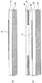
図5は、TFTアレイ基板10上に形成された相隣接する複数のサブ画素70の平面図である。TFTアレイ基板10上には、X方向及びY方向に対してマトリクス状にデータ線6及び走査線3が設けられている。
FIG. 5 is a plan view of a plurality of adjacent sub-pixels 70 formed on the
本実施形態では特に、各サブ画素の非開口領域に、本発明に係る「遮光膜」の一例を構成する、ブラックマトリクス27が対向基板20上に形成されている。ブラックマトリクス27は、カラーフィルタ26を区画するように格子状に設けられ、各サブ画素の開口領域を規定している。本実施形態では、本発明に係る「遮光膜」の一例を構成する、遮光膜11がTFTアレイ基板10上に形成されている。更に、データ線6も、本発明に係る「遮光膜」の一例を構成している。
Particularly in the present embodiment, a
即ち、本実施形態では、ブラックマトリクス27と遮光膜11とデータ線6とにより冗長的に又は協働にて、格子状の遮光領域が構築され、即ち、各サブ画素の開口領域が規定されている。遮光膜11は、TFTアレイ基板10の裏側(図2又図7中、下側)から戻り光(即ち、入射光がTFTアレイ基板の裏面で反射してなる光や、3板式プロジェクタで他の液晶ライトバルブから合成光学系を突き抜けてくる光など)がTFTに入射するのを防ぐべく、TFTアレイ基板10上に形成されている。また、このような遮光膜11は、走査線を兼ねてもよい。このように本発明に係る「遮光膜」は三つの別層から構成されているので、例えば、ブラックマトリクスは、格子状で無くストライプ状でもよいし、遮光膜11は、格子状で無くストライプ状でもよい。或いは、ブラックマトリクス27及び遮光膜11は夫々、格子状でもよく、いずれかの幅が広くてもよいし、狭くてもよい。基板貼合せのズレがないが故に画素電極との位置ズレが小さい遮光膜11の方に、各サブ画素の開口領域を規定する役割を負わせ、ブラックマトリクス27には、補助的な役割を持たせると、後述の重畳領域の幅の精度を高める上では有利である。この意味では、例えば反転駆動方式との関係で、相対的に横電界が発生し易い方向について、遮光膜11に各サブ画素の開口領域を規定する役割を負わせ、相対的に横電界の発生し難い方向について、ブラックマトリクス27に各サブ画素の開口領域を規定する役割を負わせると有利である。
That is, in the present embodiment, a grid-like light shielding region is constructed by the
本実施形態では、走査線3を構成している配線は透明な素材で形成されてもよい。更に、ブラックマトリクス27と遮光膜11との二者から本発明に係る「遮光膜」を構成するのであれば、データ線6についても透明な材料で形成されてもよい。但し、配線抵抗を低める等の観点から、データ線6は、アルミニウム等の導電性金属から形成される。
In the present embodiment, the wiring constituting the
本実施形態においては特に、データ線6は遮光膜11よりも幅広に形成されており、各サブ画素70間の開口領域を規定している。尚、後述するように、データ線6は、対向基板20上に形成されたブラックマトリクス27の幅と同程度或いは少々広めに幅を有するように形成されている。
Particularly in the present embodiment, the
このように本実施形態では、データ線6によって、開口領域が規定されている。夫々の開口領域には、複数の透明な画素電極9(点線部9´により輪郭が示されている)が設けられている。特に、この画素電極9は、その縁部においてデータ線6と平面的に見て重畳部分を有するように形成されている。即ち、画素電極9と、開口領域を規定するデータ線6とは、次に詳述するように、平面的に見て重畳領域を有するように配置されている。
Thus, in the present embodiment, the opening area is defined by the
ここで図6は、本発明に係る「遮光膜」と画素電極9の位置関係を図式的に示した模式図である。遮光膜11は格子状に形成され、その上に画素電極9が形成されている。画素電極9の外縁9’は、遮光膜上に位置しており、重畳領域12(即ち、12x及び12y)を有するように形成されている。ここで、重畳領域12xは、開口領域のX方向に沿った縁部に形成された重畳領域である。重畳領域12yは、開口領域のY方向に沿った縁部に形成された重畳領域である。重畳領域12は遮光膜11で規定された開口領域の縁部分を囲むように、X方向及びY方向に存在している。
FIG. 6 is a schematic diagram schematically showing the positional relationship between the “light-shielding film” and the
次に、図7を参照して、TFTアレイ基板10上に形成されたサブ画素70の階層構造について詳細に説明する。図7は、図5のV−V’線断面図である。
Next, the hierarchical structure of the sub-pixel 70 formed on the
TFTアレイ基板10上には、遮光膜11が形成され、該遮光膜11は下地絶縁膜14によって覆われている。遮光膜11は、TFTアレイ基板10上でマトリクス状に形成されており、TFTアレイ基板10の裏側からの戻り光がTFT(図7において省略)に入射するのを防いでいる。遮光膜11は、対向基板20上に形勢されたブラックマトリクス27に比べて幅狭に形成されている。そのため、遮光膜11とブラックマトリクス27は重畳的に又は協働にて、各サブ画素の開口領域を規定している。尚、遮光膜11は、例えば、Ti、Cr、W、Ta、Mo、Pd等の高融点金属のうちの少なくとも一つを含む、金属単体、合金、金属シリサイド、ポリシリサイド、これらを積層したもの等からなる。
A
データ線6は、その上面が平坦化された層間絶縁膜14を下地として形成されている。データ線6は、例えば、Al−Si−Cu、Al−Cu等のAl(アルミニウム)含有材料、又はAl単体、若しくはAl層とTiN層等との多層膜からなる。
The
データ線6上には、層間絶縁膜15を介して、画素電極9が島状に設けられており、その上側には、ラビング処理等の所定の配向処理が施された配向膜16が設けられている。画素電極9は、例えばITO(Indium Tin Oxide)膜などの透明導電性膜からなり、配向膜16は、ポリイミド膜などの有機膜からなる。
A
対向基板20上(図7では、対向基板20の下側)には、下地絶縁膜22を介してカラーフィルタ26、ブラックマトリクス27、平坦化膜28、対向電極21及び配向膜23が設けられている。特に、ブラックマトリクスは、TFTアレイ基板10上に形成されているデータ線6と共に開口領域を規定している。
A
TFTアレイ基板10上に形成された画素電極9及び遮光膜11は、重畳領域12を形成している。TFTアレイ基板10と対向基板20との間には、液晶50が形成されており、画素電極9からの電界が印加されていない状態で配向膜16及び23により所定の配向状態をとっている。ここで、TFTアレイ基板10と対向基板20とは、前述のギャップ材の存在によって、一定距離だけ離れて配置されている。この距離を基板間ギャップ距離X[μm]と規定する。
The
また、TFTアレイ基板10上において、画素電極9はサブ画素70毎(図7においては70B及び70C毎)に形成されている。ここで、隣接する画素電極9間の距離をa[μm]とし、開口領域を規定するブラックマトリクス27及びデータ線6の幅をb[μm]とすると、重畳領域12の幅(即ち、重畳幅)Y[μm]は、次式
Y=(b−a)/2 ・・・ (1)式
で表すことができる。
On the
図8に、実際に本願発明者が試作をした液晶装置における液晶50の誘電率異方性Δε、基板間ギャップ距離X、画素電極9間の距離a、データ線の幅b、重畳幅Yの夫々の値を示してある。ここに、液晶50はTN液晶であり、Δεは正の値をとる。
FIG. 8 shows the dielectric anisotropy Δε of the
図8に示した通りに液晶装置の寸法を規定すると、サブ画素間に生ずる横電界の影響を抑制できることが、本願発明者の研究によって判明している。 It has been found by the inventor's research that if the dimensions of the liquid crystal device are defined as shown in FIG. 8, the influence of the transverse electric field generated between the sub-pixels can be suppressed.
ここで、図8に示した値をもとに、図9に、横軸に基板間ギャップ距離X、縦軸に重畳幅Yをプロットした結果を示す。図9では、液晶50の誘電率異方性Δε毎に2つずつデータ点をプロットしている。本願発明者の実験により、基板間ギャップ距離Xと重畳幅Yには正比例関係があることが判明している。従って、図9に示すように、各誘電率異方性Δεにおける2つのデータ点は、夫々直線で近似することができる。この近似直線は、縦軸切片をyとすると、次式
Y=0.625X−y
で表すことができる。また、本願発明者の実験では、重畳幅Yがこの式から求められる値よりも大きく形成していれば、サブ画素間における横電界の影響を抑制できることが判明している。即ち、重畳幅Yが次式
Y≧0.625X−y ・・・ (2)式
を満足するように重畳領域の幅Yを設定すれば、隣接するサブ画素70間に生じる横電界の影響を抑制することができる。
Here, based on the values shown in FIG. 8, FIG. 9 shows the result of plotting the inter-substrate gap distance X on the horizontal axis and the overlapping width Y on the vertical axis. In FIG. 9, two data points are plotted for each dielectric anisotropy Δε of the
Y = 0.625X-y
Can be expressed as Further, in the experiments by the inventors of the present application, it has been found that the influence of the lateral electric field between the sub-pixels can be suppressed if the overlapping width Y is formed larger than the value obtained from this equation. That is, the overlapping width Y is expressed by the following equation:
Y ≧ 0.625X−y (2) If the width Y of the overlapping region is set so as to satisfy the expression (2), the influence of the horizontal electric field generated between the adjacent sub-pixels 70 can be suppressed.
図9によると、一定のΔεのもとでは、基板間ギャップ距離Xと重畳幅Yとは、比例関係を有する。即ち、基板間ギャップ距離Xが大きくなると、液晶50の配向を制御するために基板間に印加された縦電界を大きくする必要があるため、サブ画素70間に生ずる横電界の影響が相対的に増大する。そのため、横電界の影響を低減するために必要な重畳幅Yも大きくする必要がある。逆に、基板間ギャップ距離Xが小さくなると、基板間の縦電界が小さくなるため、サブ画素70間に生じる横電界の大きさも相対的に小さくとも済む。その結果、横電界の影響を低減するために必要な重畳幅も小さくなる。
According to FIG. 9, under a constant Δε, the inter-substrate gap distance X and the overlapping width Y have a proportional relationship. That is, as the inter-substrate gap distance X increases, it is necessary to increase the vertical electric field applied between the substrates in order to control the alignment of the
次に、図10は、縦軸に(2)式のy切片の値、横軸に誘電率異方性Δεをプロットした図である。図10に示した3つのデータ点は、夫々、図9における3つの誘電率異方性Δεの値に対応している。図10にプロットした各データ点の近似曲線を求めた結果、(2)式のy切片と誘電率異方性Δεとの間には次式
y=−0.0208Δε2+0.5625Δε−3.0417 ・・・ (3)式
の関係が成り立つことが判明している。
Next, FIG. 10 is a diagram in which the y-intercept value of the equation (2) is plotted on the vertical axis and the dielectric anisotropy Δε is plotted on the horizontal axis. The three data points shown in FIG. 10 correspond to the values of the three dielectric anisotropies Δε in FIG. 9, respectively. As a result of obtaining an approximate curve of each data point plotted in FIG. 10, the following equation y = −0.0208Δε 2 + 0.5625Δε−3. 0417 ... It has been found that the relationship of the expression (3) holds.
図10によると、基板間ギャップ距離Xが一定である場合、誘電率異方性Δεを大きくすると、図9におけるy切片の値は増加する。即ち、誘電率異方性Δεが大きくなると、横電界に対して敏感に液晶50が反応するようになるため、横電界の影響を低減するために必要な重畳幅Yも大きくしなければならないことを表している。
According to FIG. 10, when the inter-substrate gap distance X is constant, increasing the dielectric anisotropy Δε increases the y-intercept value in FIG. That is, when the dielectric anisotropy Δε increases, the
尚、重畳領域の幅Yが(2)式を満たさない場合には、基板間に生ずる縦電界の大きさに比べ横電界が相対的に大きくなるため、横電界の影響が顕著になり、液晶50が配向乱れを起こすことになる。 If the width Y of the overlapping region does not satisfy the expression (2), the horizontal electric field is relatively larger than the vertical electric field generated between the substrates, so that the influence of the horizontal electric field becomes significant. 50 will cause alignment disorder.
図9及び図10から、(2)式に従って液晶装置を構成すれば、重畳領域12付近における遮光領域の幅を、不必要に広げないで済む。しかも、液晶ドメインが見えないようにしつつ遮光領域の幅を小さくする(言い換えれば、光の利用効率を高める)際の限界の値を、Y=0.625X−yとして、与えてくれる。
9 and 10, if the liquid crystal device is configured according to the equation (2), it is not necessary to unnecessarily widen the width of the light shielding region in the vicinity of the overlapping
以上説明したように、本実施形態に係る液晶装置100によれば、(2)式を満たす重畳領域を設けることによって、隣接するサブ画素間に生ずる横電界の影響を抑制することができる。その結果、画素ピッチの小さい単板式の液晶装置において高品質なカラー画像表示を実現することができる。
<1−3:第1変形例>
次に、本実施形態の変形例について図11を参照して説明する。本変形例では、開口領域の縁部に形成された重畳領域12のうち、Y方向に形成された部分12yについては、上記(2)式を満足するように設けられているものの、X方向に形成された部分12xについては上記(2)式を満足しないように設けられている。ここで、本変形例における開口領域は長方形に形成されており、Y方向に沿った辺は、X方向に沿った辺よりも長い。そのため、開口領域の長辺部分であるX方向に沿った辺についてのみ上記(2)式を満たすように重畳領域12yを形成することで、効率的に隣接するサブ画素に異なる電圧が印加されることにより生じる横電界を抑制することができる。即ち、開口領域のX方向に沿った辺に形成された重畳領域12xについてのみ、上記(2)式を満たすように形成した場合に比べて、効率的に横電界を抑制することができる。
As described above, according to the
<1-3: First Modification>
Next, a modification of the present embodiment will be described with reference to FIG. In this modification, the
尚、開口領域の短辺方向であるX方向に形成された重畳領域12xについてのみ上記(2)式を満足するように形成した場合であっても、サブ画素70間に生ずる横電界の影響を軽減できるという本発明の効果をある程度得ることが可能である。
<1−4:第2変形例>
続いて、他の変形例について、図12を参照して説明する。ここでは、データ線6及び走査線3に遮光性を有する素材を用いることにより、別途遮光膜(例えば、図7における遮光膜11)を設けることなく、開口領域を規定している。尚、対向基板20上にはブラックマトリクス27が設けられており、データ線6及び走査線3と共に開口領域を規定している。
Even when the
<1-4: Second Modification>
Next, another modification will be described with reference to FIG. Here, by using a light-shielding material for the
図12は、本変形例に係る電気光学装置の画像表示領域10aにおける断面図である。TFTアレイ基板10上には、下地絶縁膜14を介して、データ線6が形成されている。データ線の上層については、図7で説明した液晶装置100と同様である。
FIG. 12 is a cross-sectional view of the
この場合、液晶50の誘電率異方性をΔε、基板間ギャップ距離X、隣接する画素電極9間の距離をa、遮光膜として機能するデータ線6の長さをbとすると、重畳幅Y[μm]は、上記(1)式を満足するように形成されている。即ち、このような重畳領域を有するように、データ線6の幅b及び画素電極9間の間隔aを規定することにより、隣接するサブ画素に異なる電圧が印加されることにより生じる横電界の影響を抑制することが可能である。
In this case, if the dielectric anisotropy of the
特に、本変形例の場合、図7のように、TFTアレイ基板10上に遮光膜11を別途設ける必要がないため、TFTアレイ基板10上の階層構造を単純化することができる。そのため、より単純な構造の電気光学装置において高品質なカラー表示を実現することができる。
<第3変形例>
続いて、図13を参照して他の変形例を説明する。ここでは、TFTアレイ基板10上に遮光膜11が幅bで設けられ、TFTアレイ基板10上に形成されたデータ線6と対向基板20上に形成されたブラックマトリクス27は遮光膜11よりも小さめに設けられている。この変形例では特に、データ線6によって開口領域が規定されていない。開口領域は、主に遮光膜11によって規定されており、遮光膜11よりも幅狭に形成されたデータ線6及びブラックマトリクス27は遮光膜11の遮光性を補助的に助けている。尚、開口領域は、遮光膜11とブラックマトリクス27との二者により重畳的に又は協働で規定されてもよい。
In particular, in the case of this modification, it is not necessary to separately provide the light-shielding
<Third Modification>
Next, another modification will be described with reference to FIG. Here, the
更に、遮光膜11に限らず、データ線6の上層側又は下層側に積層された、例えばAl膜、Ti膜等の金属膜などから構成された容量線や容量電極或いはこれと同一層に形成された専用の遮光膜から、このように開口領域が規定されてもよく、更に、容量線や容量電極とブラックマトリクス27との二者により冗長的に又は協働で規定されてもよい。
Further, not only the
尚、本変形例では、対向基板20上にあるブラックマトリクス27は、遮光膜11よりも幅狭に形成されているため、開口領域の規定については寄与しない。但し、ブラックマトリクス27を設けることによって、相異なるカラーフィルタ26間に生じる光漏れや混色を防止できるので、本変形例に係る電気光学装置の画質向上に補助的に貢献している。
In this modification, the
<2:製造方法>
本実施形態に係る液晶装置100の製造方法を図14及び図15を参照しながら、工程ごとに説明する。
<2: Manufacturing method>
A method for manufacturing the
まず、図14(a)に示すように、透明基板10上に、遮光膜11を形成することにより、開口領域を形成する。遮光膜11は、例えば、Ti、Cr、W、Ta、Mo、Pd等の高融点金属のうちの少なくとも一つを含む、金属単体、合金、金属シリサイド、ポリシリサイド、これらを積層したもの等を使用するとよい。形成した遮光膜11上には下地絶縁膜14を形成し、表面を平坦化する。下地絶縁膜14上には、必要に応じてTFT、データ線6や走査線の配線等を形成する。具体的にはスパッタリング法等によって金属膜を形成した後、エッチング等によってこれらの配線を容易に形成することができる。
First, as shown in FIG. 14A, an opening region is formed by forming a
次に、図14(b)を参照して、画素電極の形成工程について説明する。画素電極9は、下地絶縁膜14上にITO(Indium Tin Oxide)等の透明材料からなる画素電極9を、サブ画素毎に所定のパターンで島状に形成する。ここで、画素電極9は、基板10上で平面的に見て該画素電極9の縁部分が開口領域の縁部と重畳部分(即ち、重畳領域12)を有するように形成される。更に、X方向及びY方向に形成されている重畳領域12の少なくとも一部分について上記(2)式を満たすように、画素電極9を形成する。尚、上記第1変形例に係る液晶装置を製造する場合には、開口領域のY方向に沿った方向に存在する重畳領域12yだけ上記(2)を満たすように、画素電極9を形成すればよい。
Next, with reference to FIG. 14B, a process for forming a pixel electrode will be described. In the
尚、第2変形例に係る液晶装置(図12参照)を製造する場合には、遮光膜11を形成する代わりに、遮光性を有するデータ線及び走査線を形成すれば足りる。即ち、図15(a)に示すように、透明基板上に直接下地絶縁膜を形成し、その上層に、遮光性を有するデータ線6及び走査線(図15において省略)を形成することで開口領域することができる。データ線6上には層間絶縁膜15が形成され、その上に、上記(4)式を少なくとも部分的に満たす重畳領域12を有するように画素電極9を形成する。
In the case of manufacturing the liquid crystal device according to the second modification (see FIG. 12), it is sufficient to form data lines and scanning lines having light shielding properties instead of forming the
画素電極9上には配向膜が形成され、TFTアレイ基板が完成する。
An alignment film is formed on the
一方、対向基板20は、透明基板20上に下地絶縁膜22、カラーフィルタ26、対向電極21と配向膜23を配置することで、容易に形成することができる。
On the other hand, the
最後に、完成したTFTアレイ基板と対向基板とを対向配置し、間に液晶50を封入することにより、液晶装置100が完成する。
Finally, the completed TFT array substrate and the counter substrate are arranged to face each other, and the
以上説明したように本実施形態に係る製造方法によれば、本発明に係る電気光学装置を容易に製造できる。 As described above, according to the manufacturing method according to this embodiment, the electro-optical device according to the present invention can be easily manufactured.
<3:電子機器>
次に、本実施形態に係る電気光学装置100を適用可能な電子機器の具体例について図16及び図17を参照して説明する。
<3: Electronic equipment>
Next, specific examples of electronic apparatuses to which the electro-
まず、本実施形態に係る液晶装置100を、可搬型のパーソナルコンピュータ(いわゆるノート型パソコン)の表示部に適用した例について説明する。図16は、このパーソナルコンピュータの構成を示す斜視図である。同図に示すように、パーソナルコンピュータ710は、キーボード711を備えた本体部712と、本実施形態に係る液晶装置100をパネルとして適用した表示部713とを備えている。
First, an example in which the
また、本実施形態に係る液晶装置100は、液晶テレビや、カーナビゲーション装置の表示部に適用されるのが特に好適である。例えば、カーナビゲーション装置の表示部に本実施形態に係る液晶装置100を用いることにより、運転席にいる観察者に対しては、地図の画像を表示し、助手席にいる観察者に対しては、映画などの映像を表示することができる。
The
続いて、本実施形態に係る液晶装置100を、携帯電話機の表示部に適用した例について説明する。図17は、この携帯電話機の構成を示す斜視図である。同図に示すように、携帯電話機720は、複数の操作ボタン721のほか、受話口722、送話口723とともに、本実施形態に係る液晶装置100を適用した表示部724を備える。
Next, an example in which the
なお、本実施形態に係る液晶装置100を適用可能な電子機器としては、図16に示したパーソナルコンピュータや図17に示した携帯電話機の他にも、液晶テレビ、ビューファインダ型・モニタ直視型のビデオテープレコーダ、カーナビゲーション装置、ページャ、電子手帳、電卓、ワードプロセッサ、ワークステーション、テレビ電話、POS端末、ディジタルスチルカメラなどが挙げられる。
In addition to the personal computer shown in FIG. 16 and the mobile phone shown in FIG. 17, examples of electronic devices to which the
なお、上述の電気光学装置用基板及び電気光学装置などは、上述の例にのみ限定されるものではなく、本発明の要旨を逸脱しない範囲内において種々の変更が可能であることは勿論である。 The above-described electro-optical device substrate and the electro-optical device are not limited to the above-described examples, and various changes can be made without departing from the scope of the present invention. .
本発明は、上述した実施形態に限られるものではなく、請求の範囲及び明細書全体から読み取れる発明の要旨或いは思想に反しない範囲で適宜変更可能であり、そのような変更を伴う電気光学装置用基板及び電気光学装置、並びに該電気光学装置を備えた電子機器もまた本発明の技術的範囲に含まれるものである。 The present invention is not limited to the above-described embodiments, and can be appropriately changed without departing from the gist or concept of the invention that can be read from the claims and the entire specification. For electro-optical devices with such changes The substrate, the electro-optical device, and the electronic apparatus including the electro-optical device are also included in the technical scope of the present invention.
6 データ線、 9 画素電極、 10 TFTアレイ基板、 10a 画像表示領域、 11 遮光膜、 20 対向基板、 21 対向電極、 26 カラーフィルタ、 27 ブラックマトリクス、 50 液晶、 70 サブ画素、 80 画素、 100 液晶装置 6 data lines, 9 pixel electrodes, 10 TFT array substrate, 10a image display area, 11 light shielding film, 20 counter substrate, 21 counter electrode, 26 color filter, 27 black matrix, 50 liquid crystal, 70 sub-pixels, 80 pixels, 100 liquid crystal apparatus
Claims (9)
該一対の基板間に挟持された電気光学物質と、
前記一対の基板の一方に、相交差するように配線された複数の走査線及び複数のデータ線と、
前記一対の基板の一方における前記電気光学物質に面する側に、前記複数のデータ線及び前記複数の走査線の交差に対応する画素毎に配列された複数の画素電極と、
前記一対の基板の他方に、前記複数の画素電極に前記電気光学物質を介して対向するように配置された対向電極と、
前記一対の基板の少なくとも一方に設けられ、前記一対の基板上で平面的に見て、前記画素の開口領域を少なくとも部分的に規定する遮光膜と
を備え、
前記画素電極及び前記遮光膜は、前記一対の基板上で平面的に見て、前記画素電極及び前記遮光膜が部分的に重畳するように、配置されており、
前記一対の基板間における基板間ギャップ距離X、並びに前記画素電極及び前記遮光膜が部分的に重畳する重畳幅Yは、不等式
Y≧0.625X−y
但し
y=−0.0208Δε2+0.5625Δε−3.0417
Δε=前記電気光学物質の誘電率異方性
を満たす
ことを特徴とする電気光学装置。 A pair of substrates;
An electro-optic material sandwiched between the pair of substrates;
A plurality of scanning lines and a plurality of data lines wired to cross each other on one of the pair of substrates,
A plurality of pixel electrodes arranged for each pixel corresponding to an intersection of the plurality of data lines and the plurality of scanning lines on a side facing the electro-optical material in one of the pair of substrates;
A counter electrode disposed on the other of the pair of substrates so as to face the plurality of pixel electrodes with the electro-optic material interposed therebetween;
A light-shielding film that is provided on at least one of the pair of substrates and that at least partially defines an opening region of the pixel when viewed in plan on the pair of substrates.
The pixel electrode and the light-shielding film are disposed so that the pixel electrode and the light-shielding film partially overlap each other when viewed in plan on the pair of substrates.
The inter-substrate gap distance X between the pair of substrates and the overlapping width Y where the pixel electrode and the light shielding film partially overlap are inequalities.
Y ≧ 0.625X−y
However, y = −0.0208Δε 2 + 0.5625Δε−3.0417
Δε = the electro-optical device satisfying the dielectric anisotropy of the electro-optical material.
前記基板間ギャップ距離X及び前記重畳幅Yは、前記画素電極及び前記遮光膜が前記一方の方向に沿って部分的に重畳する部分について、前記不等式を満たすことを特徴とする請求項1に記載の電気光学装置。 The opening region has a planar shape in which a long side direction coincides with one of a first direction along the scanning line and a second direction along the data line,
2. The inter-substrate gap distance X and the overlapping width Y satisfy the inequality for a portion where the pixel electrode and the light shielding film partially overlap along the one direction. Electro-optic device.
前記遮光膜は、前記サブ画素の開口領域を少なくとも部分的に規定し、
前記サブ画素は、前記第1方向及び前記第2方向に沿って配置されている
ことを特徴とする請求項1から4のいずれか一項に記載の電気光学装置。 The plurality of pixel electrodes are arranged for each of the sub-pixels corresponding to any one of R (red), G (green), and B (blue), for each pixel.
The light-shielding film at least partially defines an opening region of the sub-pixel;
The electro-optical device according to claim 1, wherein the sub-pixels are arranged along the first direction and the second direction.
該一対の基板間に挟持された電気光学物質と、
前記一対の基板の一方に、相交差するように配線された複数の走査線及び複数のデータ線と、
前記一対の基板の一方における前記電気光学物質に面する側に、前記複数のデータ線及び前記複数の走査線の交差に対応する画素毎に配列された複数の画素電極と、
前記一対の基板の他方に、前記複数の画素電極に前記電気光学物質を介して対向するように配置された対向電極と
を備え、
前記データ線及び前記走査線の少なくとも一方の配線は、遮光性の材料から構成されており、前記一対の基板上で平面的に見て、前記画素の開口領域を少なくとも部分的に規定し、
前記画素電極及び前記少なくとも一方の配線は、前記一対の基板上で平面的に見て、前記画素電極及び前記少なくとも一方の配線が部分的に重畳するように、配置されており、
前記一対の基板間における基板間ギャップ距離X、並びに前記画素電極及び前記少なくとも一方の配線が部分的に重畳する重畳幅Yは、不等式
Y≧0.625X−y
但し
y=−0.0208Δε2+0.5625Δε−3.0417
Δε=前記電気光学物質の誘電率異方性
を満たす
ことを特徴とする電気光学装置。 A pair of substrates;
An electro-optic material sandwiched between the pair of substrates;
A plurality of scanning lines and a plurality of data lines wired to cross each other on one of the pair of substrates,
A plurality of pixel electrodes arranged for each pixel corresponding to an intersection of the plurality of data lines and the plurality of scanning lines on a side facing the electro-optical material in one of the pair of substrates;
A counter electrode disposed on the other of the pair of substrates so as to oppose the plurality of pixel electrodes with the electro-optical material interposed therebetween,
At least one of the data line and the scanning line is made of a light-shielding material, and at least partially defines an opening region of the pixel when viewed in plan on the pair of substrates.
The pixel electrode and the at least one wiring are arranged so as to partially overlap the pixel electrode and the at least one wiring when viewed in plan on the pair of substrates.
An inter-substrate gap distance X between the pair of substrates and an overlap width Y in which the pixel electrode and the at least one wiring partly overlap are inequalities.
Y ≧ 0.625X−y
However, y = −0.0208Δε 2 + 0.5625Δε−3.0417
Δε = the electro-optical device satisfying the dielectric anisotropy of the electro-optical material.
前記画素電極及び前記遮光膜を、前記一対の基板上で平面的に見て、前記画素電極及び前記遮光膜が部分的に重畳するように、配置する工程を備え、
前記一対の基板間における基板間ギャップ距離X、並びに前記画素電極及び前記遮光膜が部分的に重畳する重畳幅Yは、不等式
Y≧0.625X−y
但し
y=−0.0208Δε2+0.5625Δε−3.0417
Δε=前記電気光学物質の誘電率異方性
を満たす
ことを特徴とする電気光学装置の製造方法。 A pair of substrates, an electro-optical material sandwiched between the pair of substrates, a plurality of scanning lines and a plurality of data lines wired to cross each other on one of the pair of substrates, and the pair of substrates A plurality of pixel electrodes arranged for each pixel corresponding to an intersection of the plurality of data lines and the plurality of scanning lines on the side facing the electro-optic material in one of the plurality of data lines and the other of the pair of substrates, A counter electrode disposed so as to face a plurality of pixel electrodes via the electro-optic material and at least one of the pair of substrates, and when viewed in plan on the pair of substrates, an opening of the pixel An electro-optical device manufacturing method for manufacturing an electro-optical device comprising a light shielding film that at least partially defines a region,
A step of arranging the pixel electrode and the light shielding film so that the pixel electrode and the light shielding film partially overlap each other when viewed in plan on the pair of substrates;
The inter-substrate gap distance X between the pair of substrates and the overlapping width Y where the pixel electrode and the light shielding film partially overlap are inequalities.
Y ≧ 0.625X−y
However, y = −0.0208Δε 2 + 0.5625Δε−3.0417
Δε = Dielectric anisotropy of the electro-optical material is satisfied. A method of manufacturing an electro-optical device.
前記画素電極及び前記少なくとも一方の配線を、前記一対の基板上で平面的に見て、前記画素電極及び前記少なくとも一方の配線が部分的に重畳するように、配置する工程を備え、
前記一対の基板間における基板間ギャップ距離X、並びに前記画素電極及び前記少なくとも一方の配線が部分的に重畳する重畳幅Yは、不等式
Y≧0.625X−y
但し
y=−0.0208Δε2+0.5625Δε−3.0417
Δε=前記電気光学物質の誘電率異方性
を満たす
ことを特徴とする電気光学装置の製造方法。 A pair of substrates, an electro-optical material sandwiched between the pair of substrates, a plurality of scanning lines and a plurality of data lines wired to cross each other on one of the pair of substrates, and the pair of substrates A plurality of pixel electrodes arranged for each pixel corresponding to an intersection of the plurality of data lines and the plurality of scanning lines on the side facing the electro-optic material in one of the plurality of data lines and the other of the pair of substrates, A counter electrode disposed so as to face a plurality of pixel electrodes with the electro-optic material interposed therebetween, and at least one of the data line and the scanning line is made of a light shielding material, An electro-optical device manufacturing method for manufacturing an electro-optical device that at least partially defines an opening area of the pixel when viewed in plan on the pair of substrates,
A step of arranging the pixel electrode and the at least one wiring so that the pixel electrode and the at least one wiring are partially overlapped when viewed in plan on the pair of substrates;
An inter-substrate gap distance X between the pair of substrates and an overlap width Y in which the pixel electrode and the at least one wiring partly overlap are inequalities.
Y ≧ 0.625X−y
However, y = −0.0208Δε 2 + 0.5625Δε−3.0417
Δε = Dielectric anisotropy of the electro-optical material is satisfied. A method of manufacturing an electro-optical device.
Priority Applications (1)
| Application Number | Priority Date | Filing Date | Title |
|---|---|---|---|
| JP2008157951A JP5534655B2 (en) | 2008-05-26 | 2008-06-17 | ELECTRO-OPTICAL DEVICE, MANUFACTURING METHOD THEREOF, AND ELECTRONIC DEVICE |
Applications Claiming Priority (3)
| Application Number | Priority Date | Filing Date | Title |
|---|---|---|---|
| JP2008136864 | 2008-05-26 | ||
| JP2008136864 | 2008-05-26 | ||
| JP2008157951A JP5534655B2 (en) | 2008-05-26 | 2008-06-17 | ELECTRO-OPTICAL DEVICE, MANUFACTURING METHOD THEREOF, AND ELECTRONIC DEVICE |
Publications (2)
| Publication Number | Publication Date |
|---|---|
| JP2010008437A true JP2010008437A (en) | 2010-01-14 |
| JP5534655B2 JP5534655B2 (en) | 2014-07-02 |
Family
ID=41589081
Family Applications (1)
| Application Number | Title | Priority Date | Filing Date |
|---|---|---|---|
| JP2008157951A Expired - Fee Related JP5534655B2 (en) | 2008-05-26 | 2008-06-17 | ELECTRO-OPTICAL DEVICE, MANUFACTURING METHOD THEREOF, AND ELECTRONIC DEVICE |
Country Status (1)
| Country | Link |
|---|---|
| JP (1) | JP5534655B2 (en) |
Cited By (2)
| Publication number | Priority date | Publication date | Assignee | Title |
|---|---|---|---|---|
| JP2010014760A (en) * | 2008-07-01 | 2010-01-21 | Hitachi Displays Ltd | Liquid crystal display device |
| JP2013101183A (en) * | 2011-11-07 | 2013-05-23 | Japan Display Central Co Ltd | Liquid crystal display device |
Citations (5)
| Publication number | Priority date | Publication date | Assignee | Title |
|---|---|---|---|---|
| JPH08160454A (en) * | 1994-12-09 | 1996-06-21 | Sanyo Electric Co Ltd | Liquid crystal display device |
| JP2000305114A (en) * | 1999-03-17 | 2000-11-02 | Lg Philips Lcd Co Ltd | Liquid crystal display device and its production |
| JP2001166337A (en) * | 1999-09-29 | 2001-06-22 | Seiko Epson Corp | Liquid crystal device, projection type display device and method of producing liquid crystal device |
| JP2001166321A (en) * | 1999-12-10 | 2001-06-22 | Hitachi Ltd | Liquid crystal display device |
| JP2001337346A (en) * | 2000-05-26 | 2001-12-07 | Toshiba Corp | Liquid crystal display device |
-
2008
- 2008-06-17 JP JP2008157951A patent/JP5534655B2/en not_active Expired - Fee Related
Patent Citations (5)
| Publication number | Priority date | Publication date | Assignee | Title |
|---|---|---|---|---|
| JPH08160454A (en) * | 1994-12-09 | 1996-06-21 | Sanyo Electric Co Ltd | Liquid crystal display device |
| JP2000305114A (en) * | 1999-03-17 | 2000-11-02 | Lg Philips Lcd Co Ltd | Liquid crystal display device and its production |
| JP2001166337A (en) * | 1999-09-29 | 2001-06-22 | Seiko Epson Corp | Liquid crystal device, projection type display device and method of producing liquid crystal device |
| JP2001166321A (en) * | 1999-12-10 | 2001-06-22 | Hitachi Ltd | Liquid crystal display device |
| JP2001337346A (en) * | 2000-05-26 | 2001-12-07 | Toshiba Corp | Liquid crystal display device |
Cited By (3)
| Publication number | Priority date | Publication date | Assignee | Title |
|---|---|---|---|---|
| JP2010014760A (en) * | 2008-07-01 | 2010-01-21 | Hitachi Displays Ltd | Liquid crystal display device |
| JP2013101183A (en) * | 2011-11-07 | 2013-05-23 | Japan Display Central Co Ltd | Liquid crystal display device |
| US9400409B2 (en) | 2011-11-07 | 2016-07-26 | Japan Display Inc. | Liquid crystal display |
Also Published As
| Publication number | Publication date |
|---|---|
| JP5534655B2 (en) | 2014-07-02 |
Similar Documents
| Publication | Publication Date | Title |
|---|---|---|
| TWI381231B (en) | Liquid crystal display device | |
| JP5239512B2 (en) | Electro-optical device and electronic apparatus | |
| JP5024110B2 (en) | Electro-optical device and electronic apparatus | |
| US8194217B2 (en) | Electro-optical apparatus and electronic device having particular pixel configuration | |
| US20050200793A1 (en) | In-plane switching mode liquid crystal display device and method of fabricating the same | |
| JP6028332B2 (en) | Liquid crystal device and electronic device | |
| JP2007226175A (en) | Liquid crystal device and electronic equipment | |
| JP2003207803A (en) | In-plane switching mode active matrix liquid crystal display device | |
| JP2014186121A (en) | Liquid crystal display device and driving method thereof | |
| JP2011028013A (en) | Display device and electronic apparatus | |
| WO2010131552A1 (en) | Liquid crystal display device | |
| JP2010066642A (en) | Liquid crystal display device | |
| KR20110032341A (en) | Liquid crystal display device | |
| JP2007226200A (en) | Liquid crystal device, and electronic device | |
| JPH10104664A (en) | Liquid crystal display device | |
| KR20040100903A (en) | Electro-optical device, electronic apparatus, and projection display apparatus | |
| JP2010139975A (en) | Liquid crystal display apparatus | |
| US10168581B2 (en) | Display device | |
| KR20130034744A (en) | Liquid crystal display device and method for fabricating the same | |
| JP5534655B2 (en) | ELECTRO-OPTICAL DEVICE, MANUFACTURING METHOD THEREOF, AND ELECTRONIC DEVICE | |
| JP2007192975A (en) | Electrooptical apparatus and its manufacturing method | |
| JP2008070610A (en) | Liquid crystal device, and electronic equipment | |
| JP5326460B2 (en) | Electro-optical device substrate, and electro-optical device and electronic apparatus | |
| JP2013072932A (en) | Electro-optical device and electronic apparatus | |
| JP5398897B2 (en) | Liquid crystal display |
Legal Events
| Date | Code | Title | Description |
|---|---|---|---|
| A621 | Written request for application examination |
Free format text: JAPANESE INTERMEDIATE CODE: A621 Effective date: 20110428 |
|
| RD01 | Notification of change of attorney |
Free format text: JAPANESE INTERMEDIATE CODE: A7421 Effective date: 20120327 |
|
| A977 | Report on retrieval |
Free format text: JAPANESE INTERMEDIATE CODE: A971007 Effective date: 20120822 |
|
| A131 | Notification of reasons for refusal |
Free format text: JAPANESE INTERMEDIATE CODE: A131 Effective date: 20120828 |
|
| A521 | Written amendment |
Free format text: JAPANESE INTERMEDIATE CODE: A523 Effective date: 20121016 |
|
| A02 | Decision of refusal |
Free format text: JAPANESE INTERMEDIATE CODE: A02 Effective date: 20121113 |
|
| A521 | Written amendment |
Free format text: JAPANESE INTERMEDIATE CODE: A523 Effective date: 20130206 |
|
| A911 | Transfer of reconsideration by examiner before appeal (zenchi) |
Free format text: JAPANESE INTERMEDIATE CODE: A911 Effective date: 20130214 |
|
| A912 | Removal of reconsideration by examiner before appeal (zenchi) |
Free format text: JAPANESE INTERMEDIATE CODE: A912 Effective date: 20130329 |
|
| A61 | First payment of annual fees (during grant procedure) |
Free format text: JAPANESE INTERMEDIATE CODE: A61 Effective date: 20140422 |
|
| R150 | Certificate of patent or registration of utility model |
Ref document number: 5534655 Country of ref document: JP Free format text: JAPANESE INTERMEDIATE CODE: R150 |
|
| S531 | Written request for registration of change of domicile |
Free format text: JAPANESE INTERMEDIATE CODE: R313531 |
|
| R350 | Written notification of registration of transfer |
Free format text: JAPANESE INTERMEDIATE CODE: R350 |
|
| LAPS | Cancellation because of no payment of annual fees |