JP2010005795A - Method of manufacturing liquid jet recording head - Google Patents
Method of manufacturing liquid jet recording head Download PDFInfo
- Publication number
- JP2010005795A JP2010005795A JP2008164337A JP2008164337A JP2010005795A JP 2010005795 A JP2010005795 A JP 2010005795A JP 2008164337 A JP2008164337 A JP 2008164337A JP 2008164337 A JP2008164337 A JP 2008164337A JP 2010005795 A JP2010005795 A JP 2010005795A
- Authority
- JP
- Japan
- Prior art keywords
- film
- supply port
- protective film
- liquid discharge
- etching
- Prior art date
- Legal status (The legal status is an assumption and is not a legal conclusion. Google has not performed a legal analysis and makes no representation as to the accuracy of the status listed.)
- Granted
Links
Images


Landscapes
- Particle Formation And Scattering Control In Inkjet Printers (AREA)
Abstract
Description
本発明は、液体吐出記録ヘッドの製造方法に関する。 The present invention relates to a method for manufacturing a liquid discharge recording head.
従来、インク吐出圧発生素子の上方にインクを吐出するタイプのインクジェット記録ヘッド、所謂サイドシューター型のインクジェット記録ヘッドが、特許文献1、あるいは、特許文献2に開示されている。特許文献1、あるいは、特許文献2に開示されたインクジェット記録ヘッドは、インク吐出圧発生素子が形成された基板に貫通口よりなるインク供給口を設けインク吐出圧発生素子が形成された面の裏面よりインクを供給する方式が採られている。
Conventionally,
これは、インク吐出圧発生素子形成面(インク吐出口形成面)側からインク供給を行う場合、インク吐出口と紙や布等の被記録媒体との間にインク供給部材が存在する構成となる。しかしながらインク供給部材を薄くすることが困難なため、インク吐出口と被記録媒体との距離を短くできず、着弾位置精度の低下等で十分な画像品位が得られないためである。 In this case, when ink is supplied from the ink discharge pressure generating element forming surface (ink discharge port forming surface) side, an ink supply member exists between the ink discharge port and a recording medium such as paper or cloth. . However, since it is difficult to make the ink supply member thin, the distance between the ink discharge port and the recording medium cannot be shortened, and sufficient image quality cannot be obtained due to a decrease in landing position accuracy.
近年のインクジェット記録ヘッドには、高性能化に伴い、供給口寸法のバラツキを抑えて、高精度に開口することが求められている。供給口を高精度に加工することは、吐出される液体の流抵抗に大きな影響を与える、供給口端部からヒーターまでの距離のバラツキを抑えることにつながる。供給口を高精度に加工することが実現できれば、流路部の設計自由度が増し、吐出性能の優れたインクジェット記録ヘッドを実現するためには大変有利となる。 Recent inkjet recording heads are required to open with high accuracy while suppressing variations in the dimensions of the supply port as performance increases. Processing the supply port with high accuracy leads to suppressing variation in the distance from the end of the supply port to the heater, which greatly affects the flow resistance of the discharged liquid. If it is possible to process the supply port with high accuracy, the degree of freedom in designing the flow path portion increases, which is very advantageous for realizing an ink jet recording head with excellent discharge performance.
供給口を高精度に開口するための手段の一つに、ドライエッチングがある。その中でも異方性のドライエッチングを用いれば、高精度の加工が可能であると共に、微細加工が可能である。 One means for opening the supply port with high accuracy is dry etching. Among them, if anisotropic dry etching is used, high-precision processing is possible and fine processing is possible.
一方、近年では、MEMS(Micro Electro Mechanical Systems)の分野において、シリコンの深掘り技術としてボッシュプロセスが注目を浴びている。これは、壁面への保護膜形成とドライエッチングとを交互に繰り返すRIE法(反応性イオンエッチング法)の一種である。 On the other hand, in recent years, in the field of MEMS (Micro Electro Mechanical Systems), the Bosch process has attracted attention as a silicon digging technique. This is a kind of RIE method (reactive ion etching method) in which protective film formation on a wall surface and dry etching are alternately repeated.
供給口をドライエッチングによって形成する場合、シリコン基板の一方の側にエッチングストップ層を設け、基板の他方の側にエッチングマスクを設け、基板を貫通するようにエッチングすることが一般的である。この時、シリコンとの選択比が高い上、工程的にも容易であることからエッチングストップ層として、配線等の絶縁層として使用されるシリコン系の絶縁膜を用いることが多い。 When the supply port is formed by dry etching, an etching stop layer is generally provided on one side of the silicon substrate, an etching mask is provided on the other side of the substrate, and etching is performed so as to penetrate the substrate. At this time, since the selection ratio with silicon is high and the process is easy, a silicon-based insulating film used as an insulating layer for wiring or the like is often used as an etching stop layer.
シリコン深掘り技術として上述のボッシュプロセスを用いて供給口を形成する技術が特許文献3に開示されている。特許文献3に開示されているボッシュプロセスをインクジェット記録ヘッドに採用した場合のインクジェット記録ヘッドの構成を説明するための模式的平面図が図11(a)に、図11(a)のa−a部の模式的断面図が図11に示されている。
以下、図13の図11(a)のa−a部の断面を用いた模式的工程断面図を用いて、特許文献3に開示されているボッシュプロセスを採用した場合のインクジェット記録ヘッドの構成と製造方法とを説明する。
Hereinafter, the configuration of the ink jet recording head when the Bosch process disclosed in
シリコン基板400上に熱酸化膜450、インク吐出圧発生素子となるヒーター300、保護膜となるシリコン窒化膜200、Ta(タンタル)膜100が形成され、将来インク供給口が形成される位置の保護膜となるシリコン窒化膜200、Ta膜100が除去されている状態が図11および図13(1)に示されている。
A thermal oxide film 450, a heater 300 serving as an ink discharge pressure generating element, a silicon nitride film 200 serving as a protective film, and a Ta (tantalum)
その後、流路を形成する面に保護レジスト500を塗布し、供給口エッチングが開始される面に裏面レジストを形成する。次に、供給口を形成する部位の裏面レジストを除去し裏面レジストパターン600を形成する(図13(2)参照)。
Thereafter, the
その後、裏面レジストパターン600をマスクとしてシリコン基板400をエッチングストップ層である熱酸化膜450が露出するまでボッシュプロセスを用いてシリコンエッチングを行い、供給口700が形成される(図13(3)参照)。
Thereafter, using the
次に、供給口700に露出する熱酸化膜450を、ボッシュプロセスを用いて除去した状態を示す(図13(4)参照)。
Next, a state where the thermal oxide film 450 exposed at the
次に、保護レジスト500と裏面レジストパターン600を剥離除去する(図13(5)参照)。剥離には、一般的なレジスト剥離液を用いた。
Next, the
供給口を貫通させた後、ノズルプレート800を貼り合わせることでインクジェット記録ヘッドが形成される(図13(6)参照)。ここでは、ポリイミドフィルムをレーザーで加工し、これを接着材で貼り合わせ例を示している。
After penetrating the supply port, the
しかしながらシリコン系の絶縁膜をエッチングストップ層として用いてドライエッチングを行った場合、図12に示す供給口のエッチングストップ層側の端部がエッチングされ溝状の「ノッチ」と称される形状が形成される場合がある。 However, when dry etching is performed using a silicon-based insulating film as an etching stop layer, the end portion on the etching stop layer side of the supply port shown in FIG. 12 is etched to form a groove-shaped “notch” shape. May be.
これは、非特許文献1にそのメカニズムが解説されているようにエッチングストップ層が正に帯電することにより、エッチングに寄与する正イオンの軌道が曲げられてしまい、エッチングが絶縁膜近傍で側壁方向へ進行することが原因である。ノッチは、不規則に発生し、その形状や寸法を制御することは甚だ困難である。これを防ぐため、基板バイアスを制御する技術もあるが、一般的にこのようなエッチング条件はレートが遅く、生産性を落とすことになる。
This is because, as explained in
エッチングストップ層に絶縁膜を用いた場合でも、供給口にエッチングストップ層が露出したらすぐにエッチングを停止すれば、この様な現象が発生することを防止することが可能である。しかしながら、供給口の中央部と周辺部とでエッチング速度違いがある、繰り返しエッチングを行った場合、1回ごとのエッチング速度が変化する、あるいは、基板の中央部と周辺部とでエッチング速度が異なる場合等がある。そのため、基板を貫通する供給口を形成するためには、エッチング時間を計算値よりも長く行う(オーバーエッチングする)必要がある。そのため、供給口に露出したSiN等の絶縁材料からなるエッチングストップ層を用いた場合、エッチングストップ層の帯電を防止することは難しい。 Even when an insulating film is used for the etching stop layer, such a phenomenon can be prevented from occurring if the etching is stopped as soon as the etching stop layer is exposed at the supply port. However, there is an etching rate difference between the central portion and the peripheral portion of the supply port. When repeated etching is performed, the etching rate changes every time, or the etching rate is different between the central portion and the peripheral portion of the substrate. There are cases. Therefore, in order to form the supply port that penetrates the substrate, it is necessary to perform the etching time longer than the calculated value (overetching). Therefore, when an etching stop layer made of an insulating material such as SiN exposed at the supply port is used, it is difficult to prevent the etching stop layer from being charged.
一方、特許文献4には、基板を貫通する開孔を形成する際に、ノッチの形成を回避するために、基板のエッチングが開始される面と対向する側の面全体に導電層からなるエッチングストップ層を形成することが開示されている。
On the other hand, in
また、特許文献5には、インクジェット記録ヘッドに用いる基板について、発熱抵抗体上に保護膜を2層設ける構造が開示されている。特許文献5では、発熱抵抗体直上には、共通電極と個別電極の絶縁性を保つことを目的としてSi3N4などのシリコン系の保護膜を使用し、その上に金属等の比較的粘りがあって機械的強度のあるTa等の保護膜を使用することが開示されている。
一方、ノッチの形成を防ぐために、特許文献4に示されているエッチングストップ層として基板全面に導電層を形成する方法がある。
On the other hand, in order to prevent the formation of the notch, there is a method of forming a conductive layer on the entire surface of the substrate as an etching stop layer disclosed in
しかしながら、エッチングストップ層は、供給口が形成される領域に設ける必要がある膜で、且つ、シリコン基板のエッチングが終了した後に除去する必要のある膜である。このため、導電材料からなるエッチングストップ層を新たに設ける場合、工程数の増加や位置精度等の問題がある。 However, the etching stop layer is a film that needs to be provided in a region where the supply port is formed, and a film that needs to be removed after the etching of the silicon substrate is completed. For this reason, when an etching stop layer made of a conductive material is newly provided, there are problems such as an increase in the number of processes and positional accuracy.
このため、工程数の増加を少なくし、且つ、ノッチの形成を防止する技術の開発が急務となる。 For this reason, there is an urgent need to develop a technique that reduces the increase in the number of processes and prevents the formation of notches.
本発明は、シリコン基板の上に設けられたシリコン系の絶縁膜の上に設けられた液体吐出圧力発生素子と、該液体吐出圧力発生素子の上に設けられた流路と、流路に液体を供給する基板を貫通する供給口とを有する液体吐出記録ヘッドの製造方法であって、
液体吐出圧力発生素子を形成する領域にシリコン系の絶縁膜を形成する工程と、
シリコン系の絶縁膜の上に液体吐出圧力発生素子を設ける工程と、
液体吐出圧力発生素子の上にシリコン系の絶縁膜からなる第一の保護膜を形成する工程と、
少なくともシリコン基板の将来供給口が形成される領域の端部となる領域の第一の保護膜を除去する工程と、
その後、金属材料からなる第二の保護膜を形成する工程と、
シリコン基板を貫通する供給口を、反応性イオンエッチングを用いて形成する工程と、
その後、供給口に露出する反応性イオンエッチングのエッチングストップ層となる第一の保護膜、あるいは、前記第一の保護膜および前記第二の保護膜を除去する工程と、
流路を形成する吐出口を有するノズルプレートを、供給口を覆う様に形成する工程と、を有することを特徴とする液体吐出記録ヘッドの製造方法製造方法である。
The present invention relates to a liquid discharge pressure generating element provided on a silicon-based insulating film provided on a silicon substrate, a flow path provided on the liquid discharge pressure generating element, and a liquid in the flow path. A liquid discharge recording head having a supply port penetrating a substrate for supplying
Forming a silicon-based insulating film in a region for forming the liquid discharge pressure generating element;
Providing a liquid discharge pressure generating element on a silicon-based insulating film;
Forming a first protective film made of a silicon-based insulating film on the liquid discharge pressure generating element;
Removing at least a first protective film in a region to be an end of a region where a future supply port of the silicon substrate is formed;
Thereafter, a step of forming a second protective film made of a metal material,
Forming a supply port penetrating the silicon substrate using reactive ion etching;
Thereafter, a step of removing the first protective film that becomes an etching stop layer of reactive ion etching exposed to the supply port, or the first protective film and the second protective film,
And a step of forming a nozzle plate having a discharge port for forming a flow path so as to cover the supply port.
本発明により、インクジェット記録ヘッドの吐出特性に大きな影響を及ぼすインク供給口を、高精度にかつ生産性の良く開口することが可能となる。 According to the present invention, it is possible to open an ink supply port that greatly affects the ejection characteristics of an ink jet recording head with high accuracy and high productivity.
インクジェット記録ヘッドは、インク以外の液体、例えば、有機EL等を用いることも行われているので、以下、液体吐出記録ヘッドと称する。 Since the ink jet recording head uses a liquid other than ink, for example, an organic EL, it is hereinafter referred to as a liquid discharge recording head.
発明者は、液体吐出圧力発生素子(以下、ヒーターと称す)上に設ける保護膜に着目した。保護膜には、個別電極と共通電極の絶縁性を保つことを目的とした絶縁性のシリコン窒化膜等のシリコン系の保護膜と、その上に設ける比較的粘りがあり機械的強度のあるTa等の金属材料からなる保護膜がある。Ta(タンタル)は液体吐出記録ヘッドにおいては、粘りがありしかも機械的強度があるという理由でヒーターの保護膜として用いられている。 The inventor paid attention to a protective film provided on a liquid discharge pressure generating element (hereinafter referred to as a heater). The protective film includes a silicon-based protective film such as an insulating silicon nitride film for the purpose of maintaining insulation between the individual electrode and the common electrode, and a relatively sticky and mechanically strong Ta film provided thereon. There is a protective film made of a metal material. Ta (tantalum) is used as a protective film for a heater in a liquid discharge recording head because it is sticky and has mechanical strength.
更に、Taのドライエッチングには、シリコン系の絶縁膜のエッチングにも使用するCF4などの一般的なエッチングガスを用いることが可能であることに着目した。 Further, it has been noted that for Ta dry etching, a general etching gas such as CF 4 that is also used for etching a silicon-based insulating film can be used.
尚、シリコン系の絶縁膜とは、シリコン酸化膜、シリコン窒化膜、あるいは、シリコン酸窒化膜のようなシリコン系の絶縁膜を総称している。 The silicon-based insulating film is a generic term for silicon-based insulating films such as a silicon oxide film, a silicon nitride film, or a silicon oxynitride film.
本発明は、従来の熱酸化膜に変えて、保護膜で、且つ、金属膜であるTaを、供給口のエッチングストップ層として使用するものである。そのため、エッチングストップ層として新たな金属膜を導入することなく、金属であるTaからなる保護膜をエッチングストップ層として採用することが可能となるのでノッチの発生を防止しできる。 In the present invention, Ta, which is a protective film and a metal film, is used as an etching stop layer for the supply port instead of the conventional thermal oxide film. Therefore, it is possible to adopt a protective film made of Ta, which is a metal, as an etching stop layer without introducing a new metal film as an etching stop layer, so that the generation of notches can be prevented.
この際に、エッチングストップ層全体がTa膜である必要はなく、供給口の側壁近傍(供給口の外縁部)に露出するエッチングストップ層がTa膜であれば良く、供給口の中央部に露出したエッチングストップ層はシリコン系の絶縁膜であっても良い。理由は、供給口の中央部に露出した絶縁膜が帯電し、エッチングに寄与する正イオンの軌道が曲げられても、曲げられた正イオンが供給口の側壁に到達しなければノッチが形成されないからである。 At this time, the entire etching stop layer does not need to be a Ta film, and the etching stop layer exposed in the vicinity of the side wall of the supply port (outer edge portion of the supply port) may be a Ta film, and is exposed at the center of the supply port. The etched stop layer may be a silicon-based insulating film. The reason is that even if the insulating film exposed at the center of the supply port is charged and the trajectory of positive ions contributing to the etching is bent, the notch is not formed unless the bent positive ions reach the side wall of the supply port. Because.
保護膜として使用されているTa膜を、エッチングストップ層とすることで、新たな金属膜を採用しないですむ、更に、工程数が増加することもない。 By using the Ta film used as the protective film as an etching stop layer, a new metal film can be omitted, and the number of processes does not increase.
本発明の液体吐出記録ヘッドの第1の実施の形態を、図1、2、および、3を用いて説明する。 A first embodiment of a liquid discharge recording head of the present invention will be described with reference to FIGS.
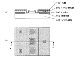
ヒーターの保護膜とエッチングストップ層とを兼ねるTaからなる保護膜を形成した状態の平面図が図2(b)に示され、図2(b)のa−a断面が図2(a)に示されている。更に、供給口が形成された状態での図2(b)のa−a断面の模式的斜視図が図1に示されている。 FIG. 2B shows a plan view of a state in which a protective film made of Ta which also serves as a protective film for the heater and an etching stop layer is formed. FIG. 2A shows a cross section taken along the line aa in FIG. It is shown. Further, FIG. 1 shows a schematic perspective view of the section aa in FIG. 2B in a state in which the supply port is formed.
図3は、図2(b)のa−a断面による第1の実施の形態の液体吐出記録ヘッドの製法を示す模式的工程断面図である。 FIG. 3 is a schematic process cross-sectional view illustrating a manufacturing method of the liquid discharge recording head according to the first embodiment, taken along a line aa in FIG.
シリコン基板400上のヒーターが形成される領域に熱酸化膜450が形成され、熱酸化膜450上にヒーター300が形成されている。ヒーター300を覆う様にシリコン窒化膜200が形成され、シリコン窒化膜200の将来供給口が形成される領域のシリコン基板400の表面が露出するように除去され、シリコン全面にTa膜100が形成されている(図2(a)、(b)参照)。
A thermal oxide film 450 is formed in a region on the
これは、シリコン基板400上にシリコン窒化膜(不図示)を形成し、その後、将来供給口を形成する領域のシリコン窒化膜を除去し、将来ヒーターを形成する領域のシリコン基板を露出させる。次に、露出したシリコン基板を、熱酸化法を用いて酸化し、熱酸化膜450を形成する。次に、熱酸化膜上にヒーター300形成後、シリコン窒化膜200を形成する。その後、シリコン窒化膜200の将来供給口が形成される領域を通常のフォトリソグラフィー法とドライエッチング法を用いて除去した後、Ta膜100が形成される。
This forms a silicon nitride film (not shown) on the
図1では更にシリコン基板がエッチング除去され、供給口の形成された状態が示されている。 FIG. 1 shows a state where the silicon substrate is further etched away and a supply port is formed.
図1および図2では、熱酸化膜450が、将来ヒーター300が形成される領域に設けられた構造が示されているが、シリコン基板400上に、熱酸化膜450、シリコン窒化膜200を形成後、供給口が形成される領域をエッチング除去しても良い。
1 and 2 show a structure in which the thermal oxide film 450 is provided in a region where the heater 300 will be formed in the future, the thermal oxide film 450 and the silicon nitride film 200 are formed on the
この場合、上述の従来技術で説明した製造方法とは工程数が増加することなく製造工程の順序が異なるだけで、同一マスクを用いて製造することができる。 In this case, the manufacturing method described in the above-described prior art can be manufactured by using the same mask only in the order of manufacturing steps without increasing the number of steps.
図3(1)(図2(a)と同じ)のようにTa膜100を形成後、シリコン基板400の流路を形成する面(Ta膜100が形成された側の面)に保護レジスト500を塗布し、供給口エッチングが開始される面に裏面レジストを塗布する。
After forming the
次に、供給口を形成する部位の裏面レジストを通常のフォトリソグラフィー法を用いて除去し裏面レジストパターン600が形成される(図3(2)参照)。 Next, the backside resist at the portion where the supply port is formed is removed using a normal photolithography method to form a backside resist pattern 600 (see FIG. 3B).
その後、裏面レジストパターン600をマスクとしてシリコン基板400をエッチングして供給口700を形成する。エッチングはエッチングストップ層であるTa膜100が露出するまで深堀りRIE(反応性イオンエッチング)の一種であるボッシュプロセスを用いて行うことが好ましい(図3(3)参照)。
Thereafter, the
次に、供給口700に露出するTa膜100を、裏面レジストパターン600をマスクとしてRIE法を用いて除去した状態を示す(図3(4)参照)。
Next, a state in which the
次に、保護レジスト500と裏面レジストパターン600とを剥離除去する(図3(5)参照)。剥離には、一般的なレジスト剥離液を用いればよい。
Next, the protective resist 500 and the back surface resist
供給口を貫通させた後、ノズルプレート800を貼り合わせることでインクジェット記録ヘッドが形成される(図3(6)参照)。ここでは、ポリイミドフィルムをレーザーで加工し、これを接着材で貼り合わせた例を示しているが、流路型材を用いることも可能である。
After penetrating the supply port, the
一方、RIE法を用いて深い開孔を形成する場合、開孔の中央部に対し、開孔の側壁近傍のエッチャントの供給量が少なくなる場合がある。この場合、パターンの中央部が外周部よりもエッチング速度が速いことがあり、開孔の側壁の近傍のエッチングストップ層が露出するまでエッチングが行われた場合、開孔の中央部ではエッチングストップ層となるTa膜が除去された部分が発生する場合ある。 On the other hand, when a deep hole is formed using the RIE method, the supply amount of the etchant in the vicinity of the side wall of the hole may be reduced with respect to the central part of the hole. In this case, the central portion of the pattern may have a higher etching rate than the outer peripheral portion, and when etching is performed until the etching stop layer near the side wall of the opening is exposed, the etching stop layer is formed in the central portion of the opening. A portion from which the Ta film is removed may occur.
第2の実施の形態は上述の問題が生じない構造を提供することを目的とするものである。以下、図4および5を用いて詳細に説明する。 The second embodiment is intended to provide a structure in which the above-described problems do not occur. This will be described in detail below with reference to FIGS.
シリコン基板400上のヒーターが形成される領域に熱酸化膜450が形成され、熱酸化膜450上にヒーター300が形成されている。ヒーター300を覆う様にシリコン窒化膜200が形成されている。シリコン窒化膜200の将来供給口が形成される領域の中央部を除いた領域が除去され、シリコン全面にTa膜100が形成されている(図4(a)、(b)参照)。
A thermal oxide film 450 is formed in a region where a heater is formed on the
これは、シリコン基板400上にシリコン窒化膜(不図示)を形成し、その後、将来供給口を形成する領域のシリコン窒化膜を除去し、将来ヒーターを形成する領域のシリコン基板を露出させる。次に、露出したシリコン基板を、熱酸化法を用いて酸化し、熱酸化膜450を形成する。次に、熱酸化膜上にヒーター300形成後、シリコン窒化膜200を形成する。その後、シリコン窒化膜200の将来供給口が形成される領域の中央部を除いた領域を通常のフォトリソグラフィー法とドライエッチング法とを用いて除去する。その後、Ta膜100が形成される。
This forms a silicon nitride film (not shown) on the
本実施の形態でも第1の実施の形態と同様に、熱酸化膜450が、将来ヒーター300が形成される領域に設けられた構造が示されているが、シリコン基板400上に、熱酸化膜450、シリコン窒化膜200を形成後、供給口が形成される領域をエッチング除去することもできる。
In the present embodiment, similarly to the first embodiment, a structure is shown in which a thermal oxide film 450 is provided in a region where the heater 300 will be formed in the future. However, a thermal oxide film is formed on the
図5は、図4(b)のa−a断面を用いた模式的工程断面図である。 FIG. 5 is a schematic process cross-sectional view using the aa cross section of FIG.
図5(1)(図4(a)と同じ)のようにTa膜100を形成後、流路を形成する面に保護レジスト500を塗布し、供給口エッチングが開始される面に裏面レジストを塗布する。
After forming the
次に、供給口を形成する部位の裏面レジストを除去し裏面レジストパターン600を形成する(図5(2)参照)。その後、裏面レジストパターン600をマスクとしてボッシュプロセスを用いてシリコンエッチングを行い、供給口700を形成する。供給口700の中央部は供給口の側壁近傍よりもエッチング速度が速い。そのために、供給口700の中央部でエッチングストップ層となるシリコン窒化膜200が露出した状態では、供給口700の側壁近傍では、シリコン基板400が残った状態である(図5(3)参照)。
Next, the backside resist at the portion where the supply port is formed is removed to form a backside resist pattern 600 (see FIG. 5B). Thereafter, silicon etching is performed using a Bosch process using the backside resist
その後、供給口700の側壁近傍でもエッチングストップ層となるTa膜が露出するまでさらにエッチングを行うことで、シリコン基板400を貫通する供給口が形成される。供給口700の側壁近傍にエッチングストップ層が露出すると、供給口700の中央部では、ストッパー層となるシリコン窒化膜200やTa膜100がエッチングされた状態となるが、保護レジスト500が露出することはない(図5(4)参照)。
Thereafter, further etching is performed in the vicinity of the sidewall of the
次に、供給口700に露出するTa膜100およびシリコン窒化膜200を、RIE法を用いて除去した状態を示す(図5(5)参照)。
Next, a state where the
次に、保護レジスト500と裏面レジストパターン600とを剥離除去する(図5(6)参照)。剥離には、一般的なレジスト剥離液を用いた。
Next, the protective resist 500 and the back surface resist
供給口を貫通させた後、ノズルプレート800を貼り合わせることでインクジェット記録ヘッドが形成される(図5(7)参照)。ここでは、ポリイミドフィルムをレーザーで加工し、これを接着材で貼り合わせた例を示しているが、流路型材を用いることも可能である。
After penetrating the supply port, the
一方、Taは一般的に応力が大きく、成膜条件によっては、供給口エッチング後の状態において剥がれなどの現象を生じる場合がある。 On the other hand, Ta generally has a large stress, and depending on the film forming conditions, a phenomenon such as peeling may occur in the state after the supply port etching.
第3の実施の形態は上述の問題が生じない構造を提供することを目的とするものである。 The third embodiment is intended to provide a structure that does not cause the above-described problems.
上述の問題が発生することを防止するために、図4に示す供給口の中央部に残したシリコン窒化膜200の中央部のTa膜100の一部を除去しTa膜100の応力を分散させることでTa膜100の剥がれ等の現象を防止することができる。
In order to prevent the above problem from occurring, a part of the
以下、図6および7を用いて詳細に説明する。 This will be described in detail below with reference to FIGS.
シリコン基板400上のヒーターが形成される領域に熱酸化膜450が形成され、熱酸化膜450上にヒーター300が形成されている。ヒーター300を覆う様にシリコン窒化膜200が形成されている。シリコン窒化膜200の将来供給口が形成される領域の中央部を除いた領域が除去されている。供給口700の中央部となる領域に残されたシリコン窒化膜200上に形成されたTa膜100が除されている(図6(a)、(b)参照)。
A thermal oxide film 450 is formed in a region on the
これは、シリコン基板400上にシリコン窒化膜(不図示)を形成し、その後、将来供給口を形成する領域のシリコン窒化膜を除去し、将来ヒーターを形成する領域のシリコン基板を露出させる。次に、露出したシリコン基板を、熱酸化法を用いて酸化し、熱酸化膜450を形成する。次に、熱酸化膜上にヒーター300形成後、シリコン窒化膜200を形成する。その後、シリコン窒化膜200の将来供給口が形成される領域の中央部を除いた領域を通常のフォトリソグラフィー法とドライエッチング法とを用いて除去する。その後、Ta膜100が形成される。
This forms a silicon nitride film (not shown) on the
その後、Ta膜100を形成し、通常のフォトリソグラフィー法とドライエッチング法とを用いて供給口700の中央部となる領域に残されたシリコン窒化膜200上に形成されたTa膜100を除去する。
Thereafter, a
本実施の形態でも第1の実施の形態と同様に、熱酸化膜450が、将来ヒーター300が形成される領域に設けられた構造が示されているが、シリコン基板400上に、熱酸化膜450、シリコン窒化膜200を形成後、供給口が形成される領域をエッチング除去することもできる。
In the present embodiment, similarly to the first embodiment, a structure is shown in which a thermal oxide film 450 is provided in a region where the heater 300 will be formed in the future. However, a thermal oxide film is formed on the
図7は、図6(b)のa−a断面を用いた模式的工程断面図である。 FIG. 7 is a schematic process cross-sectional view using the aa cross section of FIG.
図7(1)(図6(a)と同じ)のようにTa膜100を形成し、供給口700の中央部となる領域に残したシリコン窒化膜200上に形成されたTa膜100を除去した後、流路を形成する面に保護レジスト500を、供給口エッチングが開始される面に裏面レジストを塗布する。
The
次に、供給口を形成する部位の裏面レジストを除去し裏面レジストパターン600を形成する(図7(2)参照)。その後、裏面レジストパターン600をマスクとしてボッシュプロセスを用いてシリコンエッチングを行い、エッチングストップ層となるTa膜が露出するまでされにエッチングを行う(図7(3)参照)。
Next, the backside resist at the portion where the supply port is formed is removed to form a backside resist pattern 600 (see FIG. 7B). Thereafter, silicon etching is performed using a Bosch process with the backside resist
次に、供給口700に露出するTa膜100およびシリコン窒化膜200を、RIE法を用いて除去した状態を示す(図7(4)参照)。
Next, a state where the
次に、保護レジスト500と裏面レジストパターン600とを剥離除去する(図7(5)参照)。剥離には、一般的なレジスト剥離液を用いることができる。
Next, the protective resist 500 and the back surface resist
シリコン基板400を貫通する供給口を形成した後、ノズルプレート800を貼り合わせることでインクジェット記録ヘッドが形成される(図7(6)参照)。ここでは、ポリイミドフィルムをレーザーで加工し、これを接着材で貼り合わせた例を示しているが、流路型材を用いることも可能である。
After the supply port penetrating the
本発明の第4の実施の形態として供給口内にフィルターを形成した例を図8および9を用いて説明する。 An example in which a filter is formed in the supply port will be described with reference to FIGS. 8 and 9 as a fourth embodiment of the present invention.
シリコン基板400上のヒーターが形成される領域に熱酸化膜450が形成され、熱酸化膜450上にヒーター300が形成されている。ヒーター300を覆う様にシリコン窒化膜200が形成され、シリコン窒化膜200の将来供給口が形成される領域除去され、Ta膜100がシリコン基板400上に形成されている。更に、Ta膜100の供給口700が形成される領域と対向する位置にフィルター層900が設けられている(図8(a)、(b)参照)。
A thermal oxide film 450 is formed in a region on the
これは、シリコン基板400上にシリコン窒化膜(不図示)を形成し、その後、将来供給口を形成する領域のシリコン窒化膜を除去し、将来ヒーターを形成する領域のシリコン基板を露出させる。次に、露出したシリコン基板を、熱酸化法を用いて酸化し、熱酸化膜450を形成する。次に、熱酸化膜上にヒーター300形成後、シリコン窒化膜200を形成する。その後、シリコン窒化膜200の将来供給口が形成される領域の中央部を除いた領域を通常のフォトリソグラフィー法とドライエッチング法とを用いて除去する。その後、Ta膜100が形成される。次に、Ta膜100の供給口700が形成される領域と対向する位置にフィルター層900が形成される。
This forms a silicon nitride film (not shown) on the
本実施の形態においても熱酸化膜450が、将来ヒーター300が形成される領域に設けられた構造が示されているが、シリコン基板400上に、熱酸化膜450、シリコン窒化膜200を形成後、供給口が形成される領域をエッチング除去することもできる。
Also in the present embodiment, a structure in which the thermal oxide film 450 is provided in a region where the heater 300 will be formed in the future is shown. However, after the thermal oxide film 450 and the silicon nitride film 200 are formed on the
図9は、図8(b)のa−a断面を用いた模式的工程断面図である。 FIG. 9 is a schematic process cross-sectional view using the aa cross section of FIG.
図9(1)(図8(a)と同じ)のようにTa膜100を形成し、その後、Ta膜100の供給口700が形成される領域と対向する位置にフィルター層900を設けた後、流路を形成する面に保護レジスト500を、供給口エッチングが開始される面に裏面レジストを塗布する。
After forming the
次に、供給口を形成する部位の裏面レジストを除去し裏面レジストパターン600を形成する(図9(2)参照)。その後、裏面レジストパターン600をマスクとしてエッチングストップ層であるTa膜100が露出するまでボッシュプロセスを用いてシリコンエッチングを行い、供給口700を形成する(図9(3)参照)。
Next, the backside resist at the portion where the supply port is formed is removed to form a backside resist pattern 600 (see FIG. 9B). Thereafter, silicon etching is performed using a Bosch process until the
次に、供給口700に露出するTa膜100を、RIE法を用いて除去した状態を示す(図9(4)参照)。
Next, a state where the
次に、保護レジスト500と裏面レジストパターン600を剥離除去する(図9(5)参照)。剥離には、一般的なレジスト剥離液を用いることができる。
Next, the protective resist 500 and the back surface resist
供給口を貫通させた後、ノズルプレート800を貼り合わせることでインクジェット記録ヘッドが形成される(図9(6)参照)。ここでは、ポリイミドフィルムをレーザーで加工し、これを接着材で貼り合わせた例を示しているが、流路型材を用いることも可能である。
After penetrating the supply port, the
本発明の第5の実施形態として、流路型材を用いた製造方法を、図10の図2(b)のa−a断面を用いた模式的工程断面図を用いて説明する。 As a fifth embodiment of the present invention, a manufacturing method using a flow path mold will be described with reference to a schematic process cross-sectional view using the aa cross-section of FIG. 2B.
シリコン基板400上のヒーターが形成される領域に熱酸化膜450が形成され、熱酸化膜450上にヒーター300が形成されている。ヒーター300を覆う様にシリコン窒化膜200が形成されている。シリコン窒化膜200の将来供給口が形成される領域の中央部を除いた領域が除去され、シリコン全面にTa膜100が形成されている(図10(1)参照)。
A thermal oxide film 450 is formed in a region on the
これは、シリコン基板400上にシリコン窒化膜(不図示)を形成し、その後、将来供給口を形成する領域のシリコン窒化膜を除去し、将来ヒーターを形成する領域のシリコン基板を露出させる。次に、露出したシリコン基板を、熱酸化法を用いて酸化し、熱酸化膜450を形成する。次に、熱酸化膜上にヒーター300形成後、シリコン窒化膜200を形成する。その後、シリコン窒化膜200の将来供給口が形成される領域の中央部を除いた領域を通常のフォトリソグラフィー法とドライエッチング法とを用いて除去する。その後、Ta膜100が形成される。
This forms a silicon nitride film (not shown) on the
その後、溶解可能な樹脂を用いて流路型材870を形成した後、流路型材870を覆うように流路壁となるノズル材850を形成する。ノズル材850のヒーター300と対向する位置に液体吐出口880を形成する。その後、ノズル材850上に保護レジスト500を塗布し、供給口のエッチングが開始される面に裏面レジストを形成する。 Thereafter, the flow path mold member 870 is formed using a soluble resin, and then the nozzle member 850 serving as a flow path wall is formed so as to cover the flow path mold member 870. A liquid discharge port 880 is formed at a position facing the heater 300 of the nozzle material 850. Thereafter, a protective resist 500 is applied on the nozzle material 850, and a backside resist is formed on the surface of the supply port where etching is started.
次に、供給口を形成する部位の裏面レジストを除去し裏面レジストパターン600を形成する(図10(2)参照)。 Next, the backside resist at the portion where the supply port is formed is removed to form a backside resist pattern 600 (see FIG. 10B).
その後、裏面レジストパターン600をマスクとしてエッチングストップ層であるTa膜100が露出するまでボッシュプロセスを用いてシリコンエッチングを行い、供給口700を形成する(図10(3)参照)。
Thereafter, silicon etching is performed using a Bosch process until the
次に、供給口700に露出するTa膜100を、RIE法を用いて除去した状態を示す(図10(4)参照)。
Next, a state in which the
次に、保護レジスト500と裏面レジストパターン600を剥離除去する(図10(5)参照)。剥離には、一般的なレジスト剥離液を用いた。
Next, the protective resist 500 and the back surface resist
その後、液体吐出口880および供給口700を介して溶媒により溶解除去し液体吐出記録ヘッドが形成される(図10(6)参照。 Thereafter, the liquid discharge recording head is formed by dissolving and removing with a solvent through the liquid discharge port 880 and the supply port 700 (see FIG. 10 (6)).
以下、本発明に基づく液体吐出記録ヘッドを実施例に基づいて説明するが、本発明はこれによって限定されるものではない。 Hereinafter, although the liquid discharge recording head based on this invention is demonstrated based on an Example, this invention is not limited by this.
(実施例)
(実施例1)
本実施例は、第1の実施形態に対応する実施例である。以下、図3の模式的工程断面図に基づいて本実施例の詳細を説明する。
(Example)
Example 1
The present example is an example corresponding to the first embodiment. The details of the present embodiment will be described below based on the schematic process cross-sectional view of FIG.
膜厚200μmのシリコン基板400上に、シリコン窒化膜を形成し、その後、熱酸化膜を形成する領域のシリコン窒化膜を除去した後、膜厚500nmの熱酸化膜450を形成した。シリコン窒化膜を除去した後、熱酸化膜450上にヒーター300と、配線(図示せず)の絶縁性を得るための第一の保護膜となるシリコン窒化膜200を形成した。その後、供給口が形成される領域のシリコン窒化膜200をドライエッチング法等のエッチング法を用いて除去し、機械的強度のある第二の保護膜となるTa膜100を形成した(図3(1)参照)。
A silicon nitride film was formed on a
シリコン窒化膜200はCVD法を用いて形成し、膜厚は300nm、Ta膜100はスパッタ法により形成し膜厚は230nmである。
The silicon nitride film 200 is formed using a CVD method, the film thickness is 300 nm, and the
次に、シリコン基板400の流路が形成する側に保護レジスト500を塗布し、供給口エッチングを開始する側に裏面レジストを形成した。その後、供給口が形成される領域の裏面レジストを除去し、裏面レジストパターン600を形成した(図3(2)参照)。
Next, a protective resist 500 was applied to the side where the flow path of the
本実施例においてはレジストを使用したが、ドライフィルムなどの材料を用いることも可能である。なお、本実施例では、保護レジスト500および裏面レジストには、東京応化工業製のOFPR800を用い、膜厚が7μmになるように塗布法を用いて形成した。 In this embodiment, a resist is used, but a material such as a dry film can also be used. In this example, the protective resist 500 and the back resist were formed of OFPR800 manufactured by Tokyo Ohka Kogyo Co., Ltd. using a coating method so as to have a film thickness of 7 μm.
次に、シリコン基板400のエッチングを、裏面レジストパターン600をマスクとして深堀りRIE法を用いて行った。シリコン基板400のエッチングは、エッチングストップ層となるTa膜100が供給口700に露出するまで行い、シリコン基板400を貫通する供給口700が形成された(図3(3)参照)。
Next, the
本実施例では、ボッシュプロセスを用いたが、ボッシュプロセスに限定する必要はなく、ボッシュプロセス以外の深堀りRIE法であってももちろん構わない。 In this embodiment, the Bosch process is used. However, the Bosch process is not necessarily limited, and a deep RIE method other than the Bosch process may be used.
ボッシュプロセスの条件は特に限定されないが、本実施例においては、プラズマパワー2000W、基板バイアス100Wとした。基板バイアスはパルス制御とし、20ms(ON)と80ms(OFF)を繰り返した。 The conditions of the Bosch process are not particularly limited, but in this embodiment, the plasma power is 2000 W and the substrate bias is 100 W. The substrate bias was controlled by pulses and repeated 20 ms (ON) and 80 ms (OFF).
供給ガスはエッチングを目的としてSF6、側壁保護を目的としてC4F8を用いた。SF6とC4F8はそれぞれ3秒と1秒ずつ交互に流し、その際の流量は、それぞれ300sccm、150sccmとし、圧力は4.8Paに設定した。また、基板温度は冷媒により20℃となるように制御した。 The supply gas was SF 6 for the purpose of etching and C 4 F 8 for the purpose of protecting the side walls. SF 6 and C 4 F 8 were alternately flowed for 3 seconds and 1 second, respectively. The flow rates at that time were 300 sccm and 150 sccm, respectively, and the pressure was set to 4.8 Pa. The substrate temperature was controlled to 20 ° C. with a refrigerant.
エッチングが進行し、供給口700がシリコン基板400を貫通すると、エッチングストップ層となるTa膜100が供給口700に露出する。Ta膜100は、金属膜であるので、エッチングストップ層が正に帯電することがないのでノッチは発生しにくい。
When the etching progresses and the
次に、エッチングストップ層であるTa膜100をCF4などのガスを用い、ドライエッチング法を用いて除去した(図3(4)参照)。
Next, the
その後、保護レジスト500と裏面レジストパターン600とレジスト剥離液を用いて除去した(図3(5)参照)。剥離液としては、OFPR800用の剥離液を用いることが出来る。
Then, it removed using the protective resist 500, the back surface resist
次に、ノズルプレート800を貼り合わせ液体吐出ヘッドが完成させた(図3(6)参照)。ノズルプレート800用の材料としては、例えば、ポリイミドフィルムを用いた。ポリイミドフィルムをレーザーで加工し、ノズルプレート800を形成した後、接着材を用いて貼り合わせた。
Next, the
本実施例においては、基体へ供給口形成後にノズルプレートを貼り合わせるプロセスを示したが、後述の実施例5に示すように、従来技術で示した流路パターンを設ける製造方法を適用できる。 In the present embodiment, the process of attaching the nozzle plate to the substrate after forming the supply port is shown. However, as shown in Example 5 described later, the manufacturing method for providing the flow path pattern shown in the prior art can be applied.
(実施例2)
本実施例は、第2の実施形態に対応する実施例である。以下、図5の模式的工程断面図に基づいて本実施例の詳細を説明する。
(Example 2)
This example is an example corresponding to the second embodiment. Hereinafter, the details of the present embodiment will be described based on the schematic process cross-sectional view of FIG.
膜厚200μmのシリコン基板400上に、シリコン窒化膜を形成し、その後、熱酸化膜を形成する領域のシリコン窒化膜を除去した後、膜厚500nmの熱酸化膜450を形成した。その後、シリコン窒化膜を除去した。次に、熱酸化膜450上にヒーター300と、配線(図示せず)の絶縁性を得るための第一の保護膜となる膜厚300nmのシリコン窒化膜200を、CVD法を用いて形成した。
A silicon nitride film was formed on a
その後、将来供給口が形成される領域の端部のシリコン窒化膜200をフォトリソグラフィー法とドライエッチング法とを用いて除去した。 Thereafter, the silicon nitride film 200 at the end of the region where the supply port is to be formed in the future was removed using a photolithography method and a dry etching method.
次に、スパッタ法を用いて膜厚230nmのTa膜100を形成した(図5(1)参照)。
Next, a
次に、シリコン基板400の流路が形成する側に保護レジスト500を塗布し、供給口エッチングを開始する側に裏面レジストを形成した。その後、供給口が形成される領域の裏面レジストを除去し、裏面レジストパターン600を形成した(図5(2)参照)。
Next, a protective resist 500 was applied to the side where the flow path of the
尚、保護レジスト500および裏面レジストには、東京応化工業製のOFPR800を用い、膜厚が7μmになるように塗布法を用いて形成した。 Note that OFPR800 manufactured by Tokyo Ohka Kogyo Co., Ltd. was used for the protective resist 500 and the backside resist, and the film thickness was 7 μm by a coating method.
本実施例においてはレジストを使用したが、ドライフィルムなどの材料を用いることも可能である。 In this embodiment, a resist is used, but a material such as a dry film can also be used.
次に、シリコン基板400を貫通する供給口700を、裏面レジストパターン600をマスクとして深堀りRIE法を用いて形成する。この際、供給口700の様に深い開孔を形成する場合、供給口700の中央部に対し、供給口700の側壁近傍のエッチャントの供給量が少なくなることがある。この様な状態が発生すると、中央部のエッチング速度に比べて壁面近傍のエッチング速度が遅くなる場合がある。この結果、供給口700の中央部ではエッチングストップ層が露出しているが、供給口700の壁面側はエッチングが終了していない場合が生じる(図5(3)参照)。
Next, a
この場合、供給口700の、供給口中央部のエッチング速度が速いため、供給口700の壁面側のエッチングが終了(供給口がシリコン基板を貫通する状態)すると、中央部はさらにエッチングが進む。この結果、供給口700の中央部ではエッチングストップ層がエッチングされてしまう(図5(4)参照)。しかしながら本実施例では、供給口700の中央部は、シリコン窒化膜200上にTa膜100が形成された2層構造となっている。このため、中央部のエッチングストップ層がなくなる可能性は小さくなる。
In this case, since the etching rate of the
本実施例では供給口の中央部には絶縁膜からなるエッチングストップ層が露出してしまうが、エッチングが終了するまで供給口の壁面近傍は、シリコン基板あるいはTa膜が露出しているので帯電は生じない。 In this embodiment, an etching stop layer made of an insulating film is exposed at the central portion of the supply port. However, since the silicon substrate or Ta film is exposed in the vicinity of the wall surface of the supply port until the etching is completed, charging is not performed. Does not occur.
深堀りRIE法としては、本実施例でもボッシュプロセスを用いた。 As the deep RIE method, the Bosch process was also used in this example.
ボッシュプロセスの条件は特に限定されないが、本実施例においては、プラズマパワー2000W、基板バイアス100Wとした。基板バイアスはパルス制御とし、20ms(ON)と80ms(OFF)を繰り返した。 The conditions of the Bosch process are not particularly limited, but in this embodiment, the plasma power is 2000 W and the substrate bias is 100 W. The substrate bias was controlled by pulses and repeated 20 ms (ON) and 80 ms (OFF).
供給ガスはエッチングを目的としてSF6、側壁保護を目的としてC4F8を用いた。SF6とC4F8はそれぞれ3秒と1秒ずつ交互に流し、その際の流量は、それぞれ300sccm、150sccmとし、圧力は4.8Paに設定した。また、基板温度は冷媒により20℃となるように制御した。 The supply gas was SF 6 for the purpose of etching and C 4 F 8 for the purpose of protecting the side walls. SF 6 and C 4 F 8 were alternately flowed for 3 seconds and 1 second, respectively. The flow rates at that time were 300 sccm and 150 sccm, respectively, and the pressure was set to 4.8 Pa. The substrate temperature was controlled to 20 ° C. with a refrigerant.
次に、エッチングストップ層であるTa膜100とシリコン窒化膜200とをCF4などのガスを用い、ドライエッチング法を用いて除去した(図5(5)参照)。
Next, the
その後、保護レジスト500と裏面レジストパターン600とレジスト剥離液を用いて除去した(図5(6)参照)。剥離液としては、OFPR800用の剥離液を用いることが出来る。
Then, it removed using the protective resist 500, the back surface resist
次に、ノズルプレート800を貼り合わせ液体吐出ヘッドが完成させた(図5(7)参照)。ノズルプレート800用の材料としては、例えば、ポリイミドフィルムを用いた。ポリイミドフィルムをレーザーで加工し、ノズルプレート800を形成した後、接着材を用いて貼り合わせた。
Next, the
本実施例においては、基体へ供給口形成後にノズルプレートを貼り合わせるプロセスを示したが、後述の実施例5に示すように、従来技術で示した流路パターンを設ける製造方法を適用できる。 In the present embodiment, the process of attaching the nozzle plate to the substrate after forming the supply port is shown. However, as shown in Example 5 described later, the manufacturing method for providing the flow path pattern shown in the prior art can be applied.
(実施例3)
Taは一般的に応力が大きく、成膜条件によっては、供給口エッチング後の状態において剥がれなどの現象を生じる場合がある。
(Example 3)
Ta generally has a large stress, and depending on the film formation conditions, a phenomenon such as peeling may occur in the state after etching of the supply port.
上述の問題が発生することを防止するために、実施例2で供給口の中央部に残したシリコン窒化膜200上のTa膜100の一部を除去しTa膜100の応力を分散させることでTa膜100の剥がれ等の現象を防止することができる。
In order to prevent the above-described problem from occurring, a part of the
以下、図7の模式的工程断面図を用いて本実施例の製造方法を詳細に説明する。 Hereafter, the manufacturing method of a present Example is demonstrated in detail using the typical process sectional drawing of FIG.
膜厚200μmのシリコン基板400上に、シリコン窒化膜を形成し、その後、熱酸化膜を形成する領域のシリコン窒化膜を除去した後、膜厚500nmの熱酸化膜450を形成した。その後、シリコン窒化膜を除去した。次に、熱酸化膜450上にヒーター300と、配線(図示せず)の絶縁性を得るための第一の保護膜となる膜厚300nmのシリコン窒化膜200を、CVD法を用いて形成した。
A silicon nitride film was formed on a
その後、将来供給口が形成される領域の端部のシリコン窒化膜200をフォトリソグラフィー法とドライエッチング法とを用いて除去した。 Thereafter, the silicon nitride film 200 at the end of the region where the supply port is to be formed in the future was removed using a photolithography method and a dry etching method.
次に、スパッタ法を用いて膜厚230nmのTa膜100を形成した後、供給口が形成される領域に設けられたシリコン窒化膜200上のTa膜100をフォトリソグラフィー法とドライエッチング法とを用いて除去した(図7(1)参照)。
Next, after forming the
次に、シリコン基板400の流路が形成する側に保護レジスト500を塗布し、供給口エッチングを開始する側に裏面レジストを形成した。その後、供給口が形成される領域の裏面レジストを除去し、裏面レジストパターン600を形成した(図7(2)参照)。
Next, a protective resist 500 was applied to the side where the flow path of the
尚、保護レジスト500および裏面レジストには、東京応化工業製のOFPR800を用い、膜厚が7μmになるように塗布法を用いて形成した。 Note that OFPR800 manufactured by Tokyo Ohka Kogyo Co., Ltd. was used for the protective resist 500 and the backside resist, and the film thickness was 7 μm by a coating method.
本実施例においてはレジストを使用したが、ドライフィルムなどの材料を用いることも可能である。 In this embodiment, a resist is used, but a material such as a dry film can also be used.
次に、シリコン基板400を裏面レジストパターン600をマスクとして深堀りRIE法を用い行った。シリコン基板400のエッチングは、エッチングストップ層となるTa膜100およびシリコン窒化膜200が供給口700に露出するまで行い、シリコン基板400を貫通する供給口700を形成した(図7(3)参照)。
Next, the
エッチングストップ層の下のシリコン基板がエッチングされ、エッチングストップ層となるTa膜100の膜応力のバランスに変化が生じても、供給口中央部分のTa膜100が除去されているため、剥がれなどの現象は起こりにくい。
Even if the silicon substrate under the etching stop layer is etched and the balance of the film stress of the
深堀りRIE法としては、本実施例でもボッシュプロセスを用いた。 As the deep RIE method, the Bosch process was also used in this example.
ボッシュプロセスの条件は特に限定されないが、本実施例においては、プラズマパワー2000W、基板バイアス100Wとした。基板バイアスはパルス制御とし、20ms(ON)と80ms(OFF)を繰り返した。 The conditions of the Bosch process are not particularly limited, but in this embodiment, the plasma power is 2000 W and the substrate bias is 100 W. The substrate bias was controlled by pulses and repeated 20 ms (ON) and 80 ms (OFF).
供給ガスはエッチングを目的としてSF6、側壁保護を目的としてC4F8を用いた。SF6とC4F8はそれぞれ3秒と1秒ずつ交互に流し、その際の流量は、それぞれ300sccm、150sccmとし、圧力は4.8Paに設定した。また、基板温度は冷媒により20℃となるように制御した。 The supply gas was SF 6 for the purpose of etching and C 4 F 8 for the purpose of protecting the side walls. SF 6 and C 4 F 8 were alternately flowed for 3 seconds and 1 second, respectively. The flow rates at that time were 300 sccm and 150 sccm, respectively, and the pressure was set to 4.8 Pa. The substrate temperature was controlled to 20 ° C. with a refrigerant.
次に、エッチングストップ層であるTa膜100とシリコン窒化膜200とをCF4などのガスを用い、ドライエッチング法を用いて除去した(図7(4)参照)。
Next, the
その後、保護レジスト500と裏面レジストパターン600とレジスト剥離液を用いて除去した(図7(5)参照)。剥離液としては、OFPR800用の剥離液を用いることが出来る。
Then, it removed using the protective resist 500, the back surface resist
次に、ノズルプレート800を貼り合わせ液体吐出ヘッドが完成させた(図7(6)参照)。ノズルプレート800用の材料としては、例えば、ポリイミドフィルムを用いた。ポリイミドフィルムをレーザーで加工し、ノズルプレート800を形成した後、接着材を用いて貼り合わせた。
Next, the
本実施例においては、基体へ供給口形成後にノズルプレートを貼り合わせるプロセスを示したが、後述の実施例5に示すように、従来技術で示した流路パターンを設ける製造方法を適用できる。 In the present embodiment, the process of attaching the nozzle plate to the substrate after forming the supply port is shown. However, as shown in Example 5 described later, the manufacturing method for providing the flow path pattern shown in the prior art can be applied.
(実施例4)
本実施例は、供給口内にフィルターを形成したもので、図9の模式的工程断面図を用いて製造方法を説明する。
Example 4
In this embodiment, a filter is formed in the supply port, and the manufacturing method will be described with reference to the schematic process cross-sectional view of FIG.
膜厚200μmのシリコン基板400上に、シリコン窒化膜を形成し、その後、熱酸化膜を形成する領域のシリコン窒化膜を除去した後、膜厚500nmの熱酸化膜450を形成した。次に、シリコン窒化膜を除去した。次に、熱酸化膜450上にヒーター300と、配線(図示せず)の絶縁性を得るための第一の保護膜となるシリコン窒化膜200を形成した。その後、供給口が形成される領域のシリコン窒化膜200をドライエッチング法等のエッチング法を用いて除去し、機械的強度のある第二の保護膜となるTa膜100を形成した。
A silicon nitride film was formed on a
その後、Ta膜100のシリコン基板400の将来供給口が形成される領域に対向する位置にフィルター層900を形成した(図9(1)参照)。
Thereafter, a
シリコン窒化膜200はCVD法を用いて形成し、膜厚は300nm、Ta膜100はスパッタ法により形成し膜厚は230nmである。
The silicon nitride film 200 is formed using a CVD method, the film thickness is 300 nm, and the
フィルター層900の材料としては、無機膜や有機膜などを用いることが可能である。フィルター形成後に供給口形成する場合、エッチングストップ層は、このフィルターへの保護層として働くことになる。
As a material of the
次に、シリコン基板400の流路が形成する側に保護レジスト500を塗布し、供給口エッチングを開始する側に裏面レジストを形成した。その後、供給口が形成される領域の裏面レジストを除去し、裏面レジストパターン600を形成した(図9(2)参照)。
Next, a protective resist 500 was applied to the side where the flow path of the
本実施例においてはレジストを使用したが、ドライフィルムなどの材料を用いることも可能である。なお、本実施例では、保護レジスト500および裏面レジストには、東京応化工業製のOFPR800を用い、膜厚が7μmになるように塗布法を用いて形成した。 In this embodiment, a resist is used, but a material such as a dry film can also be used. In this example, the protective resist 500 and the back resist were formed of OFPR800 manufactured by Tokyo Ohka Kogyo Co., Ltd. using a coating method so as to have a film thickness of 7 μm.
次に、シリコン基板400を裏面レジストパターン600をマスクとして深堀りRIE法を用い行った。シリコン基板400のエッチングは、エッチングストップ層となるTa膜100が供給口700に露出するまで行い、シリコン基板400を貫通する供給口700を形成した(図9(3)参照)。
Next, the
本実施例では、ボッシュプロセスを用いたが、ボッシュプロセスに限定する必要はなく、ボッシュプロセス以外の深堀りRIE法であってももちろん構わない。 In this embodiment, the Bosch process is used. However, the Bosch process is not necessarily limited, and a deep RIE method other than the Bosch process may be used.
ボッシュプロセスの条件は特に限定されないが、本実施例においては、プラズマパワー2000W、基板バイアス100Wとした。基板バイアスはパルス制御とし、20ms(ON)と80ms(OFF)を繰り返した。 The conditions of the Bosch process are not particularly limited, but in this embodiment, the plasma power is 2000 W and the substrate bias is 100 W. The substrate bias was controlled by pulses and repeated 20 ms (ON) and 80 ms (OFF).
供給ガスはエッチングを目的としてSF6、側壁保護を目的としてC4F8を用いた。SF6とC4F8はそれぞれ3秒と1秒ずつ交互に流し、その際の流量は、それぞれ300sccm、150sccmとし、圧力は4.8Paに設定した。また、基板温度は冷媒により20℃となるように制御した。 The supply gas was SF 6 for the purpose of etching and C 4 F 8 for the purpose of protecting the side walls. SF 6 and C 4 F 8 were alternately flowed for 3 seconds and 1 second, respectively. The flow rates at that time were 300 sccm and 150 sccm, respectively, and the pressure was set to 4.8 Pa. The substrate temperature was controlled to 20 ° C. with a refrigerant.
エッチングが進行し、供給口700がシリコン基板400を貫通すると、エッチングストップ層となるTa膜100が供給口700に露出する。Ta膜100は、金属膜であるので、エッチングストップ層が正に帯電することがないのでノッチは発生しにくい。
When the etching progresses and the
次に、エッチングストップ層であるTa膜100をCF4などのガスを用い、ドライエッチング法を用いて除去した(図9(4)参照)。
Next, the
Ta膜100は、CF4などのガスを用い、ラジカルを主体とした異方性ドライエッチングすることが可能である。その場合、例えばフィルター層900の材料が樹脂の場合、フィルター層900とエッチングストップ層となるTa膜100とのエッチング選択比を大きくすることができるのでフィルター層900へのダメージは小さくなる。
The
その後、保護レジスト500と裏面レジストパターン600とをレジスト剥離液を用いて除去した(図9(5)参照)。剥離液としては、OFPR800用の剥離液を用いることが出来る。
Thereafter, the protective resist 500 and the back surface resist
次に、ノズルプレート800を貼り合わせ液体吐出ヘッドが完成させた(図9(6)参照)。ノズルプレート800用の材料としては、例えば、ポリイミドフィルムを用いた。ポリイミドフィルムをレーザーで加工し、ノズルプレート800を形成した後、接着材を用いて貼り合わせた。
Next, the
本実施例においては、基体へ供給口形成後にノズルプレートを貼り合わせるプロセスを示したが、後述の実施例5に示すように、従来技術で示した流路パターンを設ける製造方法を適用できる。 In the present embodiment, the process of attaching the nozzle plate to the substrate after forming the supply port is shown. However, as shown in Example 5 described later, the manufacturing method for providing the flow path pattern shown in the prior art can be applied.
(実施例5)
図10には、実施例1のノズルプレートを、
(1)溶解可能な樹脂にてインク流路パターンを形成する工程と、
(2)常温にて固体状のエポキシ樹脂を含む被覆樹脂を溶媒に溶解し、これを溶解可能な樹脂層上にソルベントコートすることによって、溶解可能な樹脂層上にインク流路壁となる被覆樹脂層を形成する工程と、
(3)インク吐出圧力発生素子上方の被覆樹脂層にインク吐出口を形成する工程と、
(4)溶解可能な樹脂層を溶出する工程と、を行うことによって形成する、液体吐出記録ヘッドの製造方法を、図10の模式的工程断面図を用いて詳細に説明する。
(Example 5)
In FIG. 10, the nozzle plate of Example 1 is
(1) forming an ink flow path pattern with a soluble resin;
(2) A coating resin containing an epoxy resin that is solid at room temperature is dissolved in a solvent, and this is solvent-coated on a soluble resin layer, thereby forming a coating that becomes an ink flow path wall on the soluble resin layer. Forming a resin layer;
(3) forming an ink discharge port in the coating resin layer above the ink discharge pressure generating element;
(4) The process for eluting the soluble resin layer is described in detail with reference to the schematic cross-sectional process diagram of FIG.
膜厚200μmのシリコン基板400上に、シリコン窒化膜を形成し、その後、熱酸化膜を形成する領域のシリコン窒化膜を除去した後、膜厚500nmの熱酸化膜450を形成した。次に、シリコン窒化膜を除去した。次に、熱酸化膜450上にヒーター300と、配線(図示せず)の絶縁性を得るための第一の保護膜となるシリコン窒化膜200を形成した。その後、供給口が形成される領域のシリコン窒化膜200をドライエッチング法等のエッチング法を用いて除去し、機械的強度のある第二の保護膜となるTa膜100を形成した(図10(1)参照)。
A silicon nitride film was formed on a
シリコン窒化膜200はCVD法を用いて形成し、膜厚は300nm、Ta膜100はスパッタ法により形成し膜厚は230nmである。
The silicon nitride film 200 is formed using a CVD method, the film thickness is 300 nm, and the
その後、溶解可能な樹脂を用いて流路型材870を形成した後、流路型材870を覆うように流路壁となるノズル材850を形成した。溶解可能な樹脂としてノボラック系のポジ型のレジストを、ノズル材850にはネガ型のレジストを用いた。 Thereafter, the flow path mold member 870 was formed using a soluble resin, and then the nozzle member 850 serving as a flow path wall was formed so as to cover the flow path mold member 870. A novolac positive resist was used as the soluble resin, and a negative resist was used for the nozzle material 850.
流路型材870は、ノボラック系のポジ型のレジストをシリコン基板400上に塗布後、通常のフォトリソグラフィー法を用いてパターン形成を行った。同様にノズル材850もネガ型のレジストをシリコン基板上に塗布した後、通常のフォトリソグラフィー法を用いてパターン形成を行った。この際同時にヒーター300と対向する位置に液体吐出口880の形成も行った。
For the flow path mold 870, a novolac positive resist was applied on the
その後、ノズル材850上に保護レジスト500を塗布し、供給口のエッチングが開始される面に裏面レジストを形成した。 Then, the protective resist 500 was apply | coated on the nozzle material 850, and the back surface resist was formed in the surface where the etching of a supply port is started.
次に、供給口を形成する部位の裏面レジストを除去し裏面レジストパターン600を形成した(図10(2)参照)。 Next, the backside resist at the portion where the supply port was formed was removed to form a backside resist pattern 600 (see FIG. 10 (2)).
本実施例においてはレジストを使用したが、ドライフィルムなどの材料を用いることも可能である。なお、本実施例では、保護レジスト500および裏面レジストには、東京応化工業製のOFPR800を用い、膜厚が7μmになるように塗布法を用いて形成した。 In this embodiment, a resist is used, but a material such as a dry film can also be used. In this example, the protective resist 500 and the back resist were formed of OFPR800 manufactured by Tokyo Ohka Kogyo Co., Ltd. using a coating method so as to have a film thickness of 7 μm.
本実施例ではネガ型のレジストにたいしフォトリソグラフィー法を用いて液体吐出口880を形成したが、ノズル材850上にレジストパターンを形成し、これをマスクとして、ドライエッチングなどにより行うことも出来る。 In this embodiment, the liquid discharge port 880 is formed on the negative resist by using the photolithography method, but a resist pattern is formed on the nozzle material 850, and this can be used as a mask by dry etching or the like. .
その後、裏面レジストパターン600をマスクとしてエッチングストップ層であるTa膜100が露出するまでボッシュプロセスを用いてシリコンエッチングを行い、供給口700を形成する(図10(3)参照)。
Thereafter, silicon etching is performed using a Bosch process until the
次に、供給口700に露出するTa膜100を、RIE法を用いて除去した状態を示す(図10(4)参照)。
Next, a state in which the
次に、保護レジスト500と裏面レジストパターン600を剥離除去する(図10(5)参照)。剥離には、一般的なレジスト剥離液を用いた。
Next, the protective resist 500 and the back surface resist
供給口を貫通させた後、液体吐出口880および供給口700を介し剥離液により流路型材870を溶解除去し液体吐出記録ヘッドが形成された(図10(6)参照)。ここで剥離液は、通常のレジスト剥離液を用いた。
After passing through the supply port, the flow path mold member 870 was dissolved and removed by the stripping solution through the liquid discharge port 880 and the
(比較例)
比較例としてシリコン系の絶縁膜をエッチングストップ層に用いた例を図13の模式的工程断面図を用いて説明する。
(Comparative example)
As a comparative example, an example in which a silicon-based insulating film is used as an etching stop layer will be described with reference to a schematic process sectional view of FIG.
膜厚200μmのシリコン基板400上に、膜厚500nmmの熱酸化膜450を形成した。次に、熱酸化膜450上にヒーター300と、配線(図示せず)の絶縁性を得るための第一の保護膜となるシリコン窒化膜200およびTa膜100を形成した。その後、将来供給口が形成される領域に対応するTa膜100と、シリコン窒化膜200と、を通常のフォトリソグラフィー法とドライエッチング法とを用い除去した(図13(1)参照)。
A thermal oxide film 450 having a thickness of 500 nm was formed on a
シリコン窒化膜200はCVD法を用いて形成し、膜厚は300nm、Ta膜100はスパッタ法により形成し膜厚は230nmである。
The silicon nitride film 200 is formed using a CVD method, the film thickness is 300 nm, and the
流路を形成する面に保護レジスト500を塗布し、供給口エッチングが開始される面に裏面レジストを形成する。 A protective resist 500 is applied to the surface where the flow path is to be formed, and a back surface resist is formed on the surface where the supply port etching is started.
次に、シリコン基板400の流路が形成する側に保護レジスト500を塗布し、供給口エッチングを開始する側に裏面レジストを形成した。その後、供給口が形成される領域の裏面レジストを除去し、裏面レジストパターン600を形成した(図13(2)参照)。
Next, a protective resist 500 was applied to the side where the flow path of the
本比較例では、保護レジスト500および裏面レジストには、東京応化工業製のOFPR800を用い、膜厚が7μmになるように塗布法を用いて形成した。 In this comparative example, the protective resist 500 and the back resist were formed by using an OFPR800 manufactured by Tokyo Ohka Kogyo Co., Ltd. by a coating method so that the film thickness was 7 μm.
次に、シリコン基板400を裏面レジストパターン600をマスクとして深堀りRIE法を用い供給口700の形成した。シリコン基板400のエッチングは、エッチングストップ層となる熱酸化膜450が供給口700に露出するまで行い、シリコン基板400を貫通する供給口700を形成した(図13(3)参照)。
Next, the
本比較例では、ボッシュプロセスを用いたが、ボッシュプロセスに限定する必要はなく、ボッシュプロセス以外の深堀りRIE法であってももちろん構わない。 In this comparative example, the Bosch process is used, but it is not necessary to limit to the Bosch process. Of course, a deep RIE method other than the Bosch process may be used.
ボッシュプロセスの条件は特に限定されないが、本比較例においては、プラズマパワー2000W、基板バイアス100Wとした。基板バイアスはパルス制御とし、20ms(ON)と80ms(OFF)を繰り返した。 The conditions of the Bosch process are not particularly limited, but in this comparative example, the plasma power was 2000 W and the substrate bias was 100 W. The substrate bias was controlled by pulses and repeated 20 ms (ON) and 80 ms (OFF).
供給ガスはエッチングを目的としてSF6、側壁保護を目的としてC4F8を用いた。SF6とC4F8はそれぞれ3秒と1秒ずつ交互に流し、その際の流量は、それぞれ300sccm、150sccmとし、圧力は4.8Paに設定した。また、基板温度は冷媒により20℃となるように制御した。 The supply gas was SF 6 for the purpose of etching and C 4 F 8 for the purpose of protecting the side walls. SF 6 and C 4 F 8 were alternately flowed for 3 seconds and 1 second, respectively. The flow rates at that time were 300 sccm and 150 sccm, respectively, and the pressure was set to 4.8 Pa. The substrate temperature was controlled to 20 ° C. with a refrigerant.
次に、供給口700に露出する熱酸化膜450を、RIE法を用いて除去した(図13(4)参照)。
Next, the thermal oxide film 450 exposed at the
次に、保護レジスト500と裏面レジストパターン600を剥離除去した(図13(5)参照)。剥離には、一般的なレジスト剥離液を用いた。
Next, the protective resist 500 and the back surface resist
供給口を貫通させた後、ノズルプレート800を貼り合わせることでインクジェット記録ヘッドが形成された(図13(6)参照)。
After penetrating the supply port, the
本比較例では、図13(3)に示される様に、熱酸化膜450をエッチングストップ層として供給口700を形成する際、熱酸化膜450の帯電の影響により、シリコン基板400の熱酸化膜との界面にノッチが形成される場合があった。
In this comparative example, as shown in FIG. 13 (3), when the
実施例1−5および比較例の液体吐出記録ヘッドを組み立てて印字を行ったところ、ノッチが発生した部分において、ヒーターと供給口との距離は設定した値よりも小さくなったことにより、想定した吐出性能を得ることが出来なかった。 When the liquid discharge recording heads of Example 1-5 and the comparative example were assembled and printing was performed, the distance between the heater and the supply port was assumed to be smaller than the set value in the portion where the notch occurred. Discharge performance could not be obtained.
100 Ta(タンタル)膜
200 シリコン窒化
300 ヒーター
400 シリコン基板
450 熱酸化膜
500 保護レジスト
600 裏面レジストパターン
700 供給口
770 ノッチ
800 ノズルプレート
850 ノズル材
870 流路型材
900 フィルター層
100 Ta (tantalum) film 200 Silicon nitride 300
Claims (8)
前記液体吐出圧力発生素子を形成する領域に前記シリコン系の絶縁膜を形成する工程と、
前記シリコン系の絶縁膜の上に前記液体吐出圧力発生素子を設ける工程と、
前記液体吐出圧力発生素子の上にシリコン系の絶縁膜からなる第一の保護膜を形成する工程と、
少なくともシリコン基板の将来供給口が形成される領域の端部となる領域の前記第一の保護膜を除去する工程と、
その後、金属材料からなる第二の保護膜を形成する工程と、
前記シリコン基板を貫通する前記供給口を、反応性イオンエッチングを用いて形成する工程と、
その後、前記供給口に露出する前記反応性イオンエッチングのエッチングストップ層となる前記第一の保護膜、あるいは、前記第一の保護膜および前記第二の保護膜を除去する工程と、
前記流路を形成する吐出口を有するノズルプレートを、前記供給口を覆う様に形成する工程と、を有することを特徴とする液体吐出記録ヘッドの製造方法。 A liquid discharge pressure generating element provided on a silicon-based insulating film provided on a silicon substrate, a flow path provided on the liquid discharge pressure generating element, and supplying a liquid to the flow path A manufacturing method of a liquid discharge recording head having a supply port penetrating a substrate,
Forming the silicon-based insulating film in a region for forming the liquid discharge pressure generating element;
Providing the liquid discharge pressure generating element on the silicon-based insulating film;
Forming a first protective film made of a silicon-based insulating film on the liquid discharge pressure generating element;
Removing the first protective film in a region to be an end portion of a region where at least a future supply port of the silicon substrate is formed;
Thereafter, a step of forming a second protective film made of a metal material,
Forming the supply port penetrating the silicon substrate using reactive ion etching;
Then, removing the first protective film that becomes the etching stop layer of the reactive ion etching exposed to the supply port, or the first protective film and the second protective film,
And a step of forming a nozzle plate having an ejection port for forming the flow path so as to cover the supply port.
前記第一の保護膜の上に前記第二の保護膜が形成されていることを特徴とする請求項1に記載の液体吐出記録ヘッドの製造方法。 The etching stop layer formed in the region where the supply port is formed is the second protective film at the outer edge portion of the supply port, and the first protective film at the central portion of the supply port,
The method of manufacturing a liquid discharge recording head according to claim 1, wherein the second protective film is formed on the first protective film.
(1)溶解可能な樹脂にてインク流路パターンを形成する工程と、
(2)常温にて固体状のエポキシ樹脂を含む被覆樹脂を溶媒に溶解し、これを前記溶解可能な樹脂層上にソルベントコートすることによって、前記溶解可能な樹脂層の上に前記ノズルプレートとなる被覆樹脂層を形成する工程と、
(3)前記液体吐出圧力発生素子の上方の前記被覆樹脂層にインク吐出口を形成する工程と、
(4)前記溶解可能な樹脂層を溶出する工程と、からなることを特徴とする、請求項1から7のいずれかに記載の液体吐出記録ヘッドの製造方法。 Forming the nozzle plate comprises:
(1) forming an ink flow path pattern with a soluble resin;
(2) A coating resin containing an epoxy resin that is solid at room temperature is dissolved in a solvent, and this is solvent-coated on the soluble resin layer, whereby the nozzle plate and the nozzle plate are formed on the soluble resin layer. Forming a coating resin layer comprising:
(3) forming an ink discharge port in the coating resin layer above the liquid discharge pressure generating element;
(4) The method for manufacturing a liquid discharge recording head according to any one of claims 1 to 7, further comprising a step of eluting the soluble resin layer.
Priority Applications (1)
| Application Number | Priority Date | Filing Date | Title |
|---|---|---|---|
| JP2008164337A JP5224929B2 (en) | 2008-06-24 | 2008-06-24 | Manufacturing method of liquid discharge recording head |
Applications Claiming Priority (1)
| Application Number | Priority Date | Filing Date | Title |
|---|---|---|---|
| JP2008164337A JP5224929B2 (en) | 2008-06-24 | 2008-06-24 | Manufacturing method of liquid discharge recording head |
Publications (2)
| Publication Number | Publication Date |
|---|---|
| JP2010005795A true JP2010005795A (en) | 2010-01-14 |
| JP5224929B2 JP5224929B2 (en) | 2013-07-03 |
Family
ID=41586843
Family Applications (1)
| Application Number | Title | Priority Date | Filing Date |
|---|---|---|---|
| JP2008164337A Expired - Fee Related JP5224929B2 (en) | 2008-06-24 | 2008-06-24 | Manufacturing method of liquid discharge recording head |
Country Status (1)
| Country | Link |
|---|---|
| JP (1) | JP5224929B2 (en) |
Cited By (3)
| Publication number | Priority date | Publication date | Assignee | Title |
|---|---|---|---|---|
| JP2012101364A (en) * | 2010-11-05 | 2012-05-31 | Canon Inc | Method for manufacturing ejection element substrate |
| JP2013233795A (en) * | 2012-04-10 | 2013-11-21 | Canon Inc | Liquid ejecting head and method for producing the same |
| JP2015020285A (en) * | 2013-07-16 | 2015-02-02 | キヤノン株式会社 | Liquid discharge head and manufacturing method of the same |
Citations (9)
| Publication number | Priority date | Publication date | Assignee | Title |
|---|---|---|---|---|
| JPH06286149A (en) * | 1993-02-03 | 1994-10-11 | Canon Inc | Production of ink jet recording head |
| JPH07314684A (en) * | 1994-05-26 | 1995-12-05 | Canon Inc | Substrate for recording head and its manufacture |
| JPH11348290A (en) * | 1998-06-03 | 1999-12-21 | Canon Inc | Ink jet head and manufacture thereof |
| JP2004517755A (en) * | 2000-10-27 | 2004-06-17 | レックスマーク・インターナショナル・インコーポレーテツド | Improved inkjet printhead and method of manufacturing the same |
| JP2005144850A (en) * | 2003-11-14 | 2005-06-09 | Fuji Xerox Co Ltd | Method of manufacturing inkjet recording head |
| JP2005178364A (en) * | 2003-11-28 | 2005-07-07 | Canon Inc | Method of manufacturing inkjet recording head, inkjet recording head, and inkjet cartridge |
| JP2006137030A (en) * | 2004-11-10 | 2006-06-01 | Canon Inc | Liquid discharging recording head, and its manufacturing method |
| JP2006264034A (en) * | 2005-03-23 | 2006-10-05 | Canon Inc | Inkjet recording head and method for manufacturing inkjet recording head |
| JP2007083711A (en) * | 2005-08-23 | 2007-04-05 | Canon Inc | Manufacturing method of ink jet recording head |
-
2008
- 2008-06-24 JP JP2008164337A patent/JP5224929B2/en not_active Expired - Fee Related
Patent Citations (9)
| Publication number | Priority date | Publication date | Assignee | Title |
|---|---|---|---|---|
| JPH06286149A (en) * | 1993-02-03 | 1994-10-11 | Canon Inc | Production of ink jet recording head |
| JPH07314684A (en) * | 1994-05-26 | 1995-12-05 | Canon Inc | Substrate for recording head and its manufacture |
| JPH11348290A (en) * | 1998-06-03 | 1999-12-21 | Canon Inc | Ink jet head and manufacture thereof |
| JP2004517755A (en) * | 2000-10-27 | 2004-06-17 | レックスマーク・インターナショナル・インコーポレーテツド | Improved inkjet printhead and method of manufacturing the same |
| JP2005144850A (en) * | 2003-11-14 | 2005-06-09 | Fuji Xerox Co Ltd | Method of manufacturing inkjet recording head |
| JP2005178364A (en) * | 2003-11-28 | 2005-07-07 | Canon Inc | Method of manufacturing inkjet recording head, inkjet recording head, and inkjet cartridge |
| JP2006137030A (en) * | 2004-11-10 | 2006-06-01 | Canon Inc | Liquid discharging recording head, and its manufacturing method |
| JP2006264034A (en) * | 2005-03-23 | 2006-10-05 | Canon Inc | Inkjet recording head and method for manufacturing inkjet recording head |
| JP2007083711A (en) * | 2005-08-23 | 2007-04-05 | Canon Inc | Manufacturing method of ink jet recording head |
Cited By (3)
| Publication number | Priority date | Publication date | Assignee | Title |
|---|---|---|---|---|
| JP2012101364A (en) * | 2010-11-05 | 2012-05-31 | Canon Inc | Method for manufacturing ejection element substrate |
| JP2013233795A (en) * | 2012-04-10 | 2013-11-21 | Canon Inc | Liquid ejecting head and method for producing the same |
| JP2015020285A (en) * | 2013-07-16 | 2015-02-02 | キヤノン株式会社 | Liquid discharge head and manufacturing method of the same |
Also Published As
| Publication number | Publication date |
|---|---|
| JP5224929B2 (en) | 2013-07-03 |
Similar Documents
| Publication | Publication Date | Title |
|---|---|---|
| JP2008162267A (en) | Manufacturing method for inkjet printing head | |
| JP2005066890A (en) | Nozzle plate and manufacturing method therefor | |
| US8951815B2 (en) | Method for producing liquid-discharge-head substrate | |
| JP2019001125A (en) | Method for manufacturing liquid discharge head | |
| JP5224929B2 (en) | Manufacturing method of liquid discharge recording head | |
| JP4979793B2 (en) | Manufacturing method of substrate for liquid discharge head | |
| WO2005021269A1 (en) | Nozzle plate and method of producing the same | |
| US9676193B2 (en) | Substrate processing method and method of manufacturing substrate for liquid discharge head including forming hole in substrate by dry etching | |
| JP2014069567A (en) | Method of producing liquid discharging head | |
| US9371225B2 (en) | Substrate processing method | |
| TW201348010A (en) | Printhead with recessed slot ends | |
| US8808553B2 (en) | Process for producing a liquid ejection head | |
| US9205654B2 (en) | Method of manufacturing a liquid ejection head | |
| US8591007B2 (en) | Ink jet recording head and method of producing the same | |
| US9511588B2 (en) | Method for processing silicon substrate | |
| US8092700B2 (en) | Method for manufacturing liquid discharge head | |
| JP2007210242A (en) | Inkjet recording head and its manufacturing method | |
| JP4489637B2 (en) | Ink jet head and manufacturing method thereof | |
| US9168750B2 (en) | Manufacturing method of liquid discharging head | |
| JP2019166658A (en) | Method for production of base plate for liquid discharge head | |
| US7767103B2 (en) | Micro-fluid ejection assemblies | |
| JP2014030923A (en) | Substrate having through port, substrate for liquid discharge head, and method for manufacturing liquid discharge head | |
| JP2006225745A (en) | Structure of thin film element and method for producing the same | |
| JP2006062186A (en) | Nozzle plate and the manufacturing method | |
| JP2014097609A (en) | Liquid discharge head and method for manufacturing the same |
Legal Events
| Date | Code | Title | Description |
|---|---|---|---|
| A621 | Written request for application examination |
Free format text: JAPANESE INTERMEDIATE CODE: A621 Effective date: 20110614 |
|
| A977 | Report on retrieval |
Free format text: JAPANESE INTERMEDIATE CODE: A971007 Effective date: 20121114 |
|
| A131 | Notification of reasons for refusal |
Free format text: JAPANESE INTERMEDIATE CODE: A131 Effective date: 20121120 |
|
| A521 | Written amendment |
Free format text: JAPANESE INTERMEDIATE CODE: A523 Effective date: 20130121 |
|
| TRDD | Decision of grant or rejection written | ||
| A01 | Written decision to grant a patent or to grant a registration (utility model) |
Free format text: JAPANESE INTERMEDIATE CODE: A01 Effective date: 20130212 |
|
| A61 | First payment of annual fees (during grant procedure) |
Free format text: JAPANESE INTERMEDIATE CODE: A61 Effective date: 20130312 |
|
| R151 | Written notification of patent or utility model registration |
Ref document number: 5224929 Country of ref document: JP Free format text: JAPANESE INTERMEDIATE CODE: R151 |
|
| FPAY | Renewal fee payment (event date is renewal date of database) |
Free format text: PAYMENT UNTIL: 20160322 Year of fee payment: 3 |
|
| LAPS | Cancellation because of no payment of annual fees |