JP2010002664A - Optical modulation element, and method for manufacturing the same - Google Patents
Optical modulation element, and method for manufacturing the same Download PDFInfo
- Publication number
- JP2010002664A JP2010002664A JP2008161308A JP2008161308A JP2010002664A JP 2010002664 A JP2010002664 A JP 2010002664A JP 2008161308 A JP2008161308 A JP 2008161308A JP 2008161308 A JP2008161308 A JP 2008161308A JP 2010002664 A JP2010002664 A JP 2010002664A
- Authority
- JP
- Japan
- Prior art keywords
- liquid crystal
- layer
- coating
- modulation element
- light
- Prior art date
- Legal status (The legal status is an assumption and is not a legal conclusion. Google has not performed a legal analysis and makes no representation as to the accuracy of the status listed.)
- Granted
Links
Images


Landscapes
- Liquid Crystal (AREA)
- Optical Modulation, Optical Deflection, Nonlinear Optics, Optical Demodulation, Optical Logic Elements (AREA)
- Devices For Indicating Variable Information By Combining Individual Elements (AREA)
Abstract
Description
本発明は、光変調素子及びその製造方法に関する。 The present invention relates to a light modulation element and a method for manufacturing the same.
紙パルプの原料である森林資源の破壊や、ごみの廃却、焼却による環境汚染などから、オフィスを中心とする大量の紙の消費が問題になっている。しかしながら、パーソナルコンピュータの普及、インターネットを始めとする情報化社会の発達により、電子情報の一時的な閲覧を目的とする、いわゆる短寿命文書としての紙の消費は、益々増加する傾向にあり、紙に代わる書き換え可能な表示媒体の実現が望まれている。
ところで、コレステリック光変調素子は無電源で表示を保持できるメモリ性を有すること、偏光板を使用しないため明るい表示が得られること、カラーフィルターを用いずにカラー表示が可能なことなどの特長を有することから近年注目を集めている。
Consumption of a large amount of paper, especially in offices, has become a problem due to destruction of forest resources, which are raw materials for paper pulp, waste disposal, and environmental pollution caused by incineration. However, with the spread of personal computers and the development of the information society such as the Internet, the consumption of paper as a so-called short-lived document for the purpose of temporary browsing of electronic information tends to increase more and more. It is desired to realize a rewritable display medium that can replace the above.
By the way, the cholesteric light modulation element has a memory property that can hold a display with no power supply, a bright display can be obtained because a polarizing plate is not used, and a color display can be performed without using a color filter. That has attracted attention in recent years.
液晶分子が螺旋構造を持つコレステリック液晶は、入射した光を右円偏光と左円偏光に分け、螺旋の捩じれ方向に一致する円偏光成分をブラッグ反射し、残りの光を透過させる選択反射現象を起こす。反射光の中心波長λ、及び反射波長幅Δλは、螺旋ピッチをp、平均屈折率をn、複屈折率をΔnとすると、それぞれλ=n・p、Δλ=Δn・pで表され、コレステリック液晶層による反射光は螺旋ピッチに依存した鮮やかな色を呈する。
正の誘電異方性を有するコレステリック液晶は、図9(A)に示すように、螺旋軸がセル表面に垂直になり、入射光に対して上記の選択反射現象を起こすプレーナ状態、図9(B)に示すように、螺旋軸がほぼセル表面に平行になり、入射光を少し前方散乱させながら透過させるフォーカルコニック状態、及び図9(C)に示すように、螺旋構造がほどけて液晶ダイレクタが電界方向を向き、入射光をほぼ完全に透過させるホメオトロピック状態、の3つの状態を示す。
Cholesteric liquid crystals with liquid crystal molecules having a helical structure divide incident light into right and left circularly polarized light, and perform a selective reflection phenomenon that causes Bragg reflection of the circularly polarized light component that matches the twist direction of the spiral and transmits the remaining light. Wake up. The central wavelength λ of reflected light and the reflected wavelength width Δλ are expressed as λ = n · p and Δλ = Δn · p, respectively, where the helical pitch is p, the average refractive index is n, and the birefringence is Δn. The reflected light from the liquid crystal layer exhibits a vivid color depending on the helical pitch.
As shown in FIG. 9A, the cholesteric liquid crystal having positive dielectric anisotropy is in a planar state in which the helical axis is perpendicular to the cell surface and causes the selective reflection phenomenon described above with respect to incident light. As shown in FIG. 9B, the helical axis is almost parallel to the cell surface and the incident light is transmitted while being slightly scattered forward, and as shown in FIG. Shows three states: a homeotropic state in which the direction of the electric field is directed and the incident light is almost completely transmitted.
上記の3つの状態のうち、プレーナ状態とフォーカルコニック状態は、無電圧で双安定に存在することができる。したがって、コレステリック液晶の配向状態は、液晶層に印加される電圧に対して一義的に決まらず、プレーナ状態が初期状態の場合には、印加電圧の増加に伴って、プレーナ状態、フォーカルコニック状態、ホメオトロピック状態の順に変化し、フォーカルコニック状態が初期状態の場合には、印加電圧の増加に伴って、フォーカルコニック状態、ホメオトロピック状態の順に変化する。一方、液晶層に印加した電圧を急激にゼロにした場合には、プレーナ状態とフォーカルコニック状態はそのままの状態を維持し、ホメオトロピック状態はプレーナ状態に変化する。そして、印加するパルス電圧の大きさによって上記3つの状態を相互に遷移させることができる。 Of the above three states, the planar state and the focal conic state can exist bistable without voltage. Therefore, the alignment state of the cholesteric liquid crystal is not uniquely determined with respect to the voltage applied to the liquid crystal layer. When the planar state is the initial state, the planar state, the focal conic state, When the focal conic state is the initial state, the focal conic state and the homeotropic state are changed in this order as the applied voltage increases. On the other hand, when the voltage applied to the liquid crystal layer is rapidly reduced to zero, the planar state and the focal conic state are maintained as they are, and the homeotropic state is changed to the planar state. Then, the three states can be shifted to each other depending on the magnitude of the applied pulse voltage.
この電気光学応答を示したものが図10である。図10中、曲線Aは初期状態がプレーナ状態の場合を示し、曲線Bは初期状態がフォーカルコニック状態の場合を示す。
図10において(a)で示す領域はプレーナ状態またはフォーカルコニック状態(選択反射状態または透過状態)を、(b)で示す領域は遷移領域を、(c)で示す領域はフォーカルコニック状態(透過状態)を、(d)で示す領域は遷移領域を、(e)で示す領域はホメオトロピック状態を示し、ホメオトロピック状態で電圧を0にするとプレーナ状態(選択反射状態)に変化する。また、Vpf,90 、Vpf,10 、Vfh,10 、Vh,90とは、前記の2つの遷移領域の前後において、正規化反射率が90または10になる電圧(正規化反射率が90以上を選択反射状態とし、10以下を透過状態とする)を意味する。
This electro-optic response is shown in FIG. In FIG. 10, a curve A shows a case where the initial state is a planar state, and a curve B shows a case where the initial state is a focal conic state.
In FIG. 10, the region indicated by (a) is a planar state or focal conic state (selective reflection state or transmission state), the region indicated by (b) is a transition region, and the region indicated by (c) is a focal conic state (transmission state). ), A region indicated by (d) indicates a transition region, a region indicated by (e) indicates a homeotropic state, and when the voltage is set to 0 in the homeotropic state, the region changes to a planar state (selective reflection state). In addition, Vpf, 90, Vpf, 10, Vfh, 10, Vh, 90 are voltages at which the normalized reflectance is 90 or 10 before and after the two transition regions (the normalized reflectance is 90 or more). It means a selective reflection state and 10 or less is a transmission state).
そして、コレステリック液晶層の背面に、少なくとも選択反射色と同じ波長の光を吸収する層を配置することで、プレーナ状態とフォーカルコニック状態を利用した反射型メモリ表示を実現できる。 A reflective memory display using the planar state and the focal conic state can be realized by disposing at least a layer that absorbs light having the same wavelength as the selective reflection color on the back surface of the cholesteric liquid crystal layer.
コレステリック光変調素子は、一対の支持基板間に液晶を連続相として封入する構造のほかに、高分子バインダー中にコレステリック液晶をドロップ状に分散したPDLC(Polymer Dispersed Liquid Crystal)や、高分子バインダー中に液晶マイクロカプセル化された液晶を分散したPDMLC(Polymer Dispersed Microencapsulated Liquid Crystal)と称される表示方法が知られている(例えば、以下の特許文献1乃至特許文献3参照)。
Cholesteric light modulators have a structure in which liquid crystal is encapsulated as a continuous phase between a pair of supporting substrates, PDLC (Polymer Dispersed Liquid Crystal) in which cholesteric liquid crystal is dispersed in a polymer binder in the form of drops, A display method called PDMLC (Polymer Dispersed Microencapsulated Liquid Crystal) in which liquid crystal microencapsulated liquid crystal is dispersed is known (for example, see
このような反射率及び彩度の低下を抑制するために、隣接する液晶ドロップを密着させると共に液晶ドロップを多面体構造とした液晶表示素子が知られている(例えば、特許文献4参照)。 In order to suppress such a decrease in reflectance and saturation, a liquid crystal display element in which adjacent liquid crystal drops are brought into close contact with each other and the liquid crystal drops have a polyhedral structure is known (for example, see Patent Document 4).
また、ゼラチンおよび溶媒を含む溶液に液晶ドロップまたは液晶マイクロカプセルが分散された調光層用塗布液を塗布し、該調光層中の溶媒を乾燥させる液晶表示素子の製造方法が開示されている(例えば、特許文献5参照)。
しかしながら、PDLC構造やPDMLC構造のコレステリック光変調素子には、プレーナ状態での選択反射色の明るさや色純度が低く綺麗なカラー表示を行うことができないという問題や、フォーカルコニック状態での光透過率が悪く、例えば背面に黒色の光吸収層を設けた表示素子では、黒表示が白濁してコントラストが低くなるという問題がある。
また、調光層中の液晶比率が高いPDLC構造では強度が不足し、外部からの押圧等により表示特性が低下してしまう場合がある。これに対して、一般的なリブなどのスペーサーをあらかじめ設けておく方法では、規則的なリブの配列によりモアレ等の表示欠陥が発生してしまうこともある。
However, the cholesteric light modulators with PDLC structure and PDMLC structure have a problem that the brightness and color purity of the selective reflection color in the planar state is low and a beautiful color display cannot be performed, and the light transmittance in the focal conic state. However, for example, in a display element in which a black light absorption layer is provided on the back surface, there is a problem that black display becomes cloudy and the contrast becomes low.
Further, the PDLC structure having a high liquid crystal ratio in the light control layer is insufficient in strength, and the display characteristics may be deteriorated due to external pressing or the like. On the other hand, in a method in which spacers such as general ribs are provided in advance, display defects such as moire may occur due to the regular arrangement of ribs.
本発明は、上述した事情に鑑みてなされたものであり、その課題は、表示特性を低下させることなく調光層の強度を高めた光変調素子および該光変調素子の製造方法を提供することである。 The present invention has been made in view of the above-described circumstances, and an object thereof is to provide a light modulation element in which the intensity of the light control layer is increased without deteriorating display characteristics, and a method for manufacturing the light modulation element. It is.
上記課題は、以下の本発明により達成される。
すなわち本発明の請求項1に係る発明は、少なくとも一方が透光性を有し、表面に設けられた電極が対向するように配置された一対の基板と、
前記一対の基板間に設けられ、少なくとも液晶ドロップまたは液晶マイクロカプセル、高分子バインダー及び樹脂スペーサーを含む調光層と、を有する光変調素子である。
The above-mentioned subject is achieved by the following present invention.
That is, in the invention according to
A light modulation element provided between the pair of substrates and having a light control layer including at least a liquid crystal drop or a liquid crystal microcapsule, a polymer binder, and a resin spacer.
請求項2係る発明は、前記樹脂スペーサーが多角柱形状である請求項1に記載の光変調素子である。
The invention according to
請求項3に係る発明は、前記液晶ドロップまたは液晶マイクロカプセルも多角柱形状である請求項1または2に記載の光変調素子である。
The invention according to
請求項4に係る発明は、前記液晶ドロップまたは液晶マイクロカプセル及び前記樹脂スペーサーの最大長差が±50%以内である請求項1乃至3のいずれか1項に記載の光変調素子である。
The invention according to
請求項5に係る発明は、前記液晶ドロップまたは液晶マイクロカプセル及び樹脂スペーサーが、単層かつ稠密に配置されている請求項1乃至4のいずれか1項に記載の光変調素子である。
The invention according to
請求項6に係る発明は、前記調光層上に、被覆層が設けられている請求項1乃至5のいずれか1項に記載の光変調素子である。
The invention according to
請求項7に係る発明は、少なくとも一方が透光性を有し、表面に設けられた電極が対向するように配置された一対の基板と、前記一対の基板間に設けられ、少なくとも液晶ドロップまたは液晶マイクロカプセル、高分子バインダー及び樹脂スペーサーを含む調光層と、を有する光変調素子の製造方法であって、前記調光層を設ける工程が、
前記基板上に、高分子バインダー及び溶媒を含む溶液中に液晶ドロップまたは液晶マイクロカプセル及び硬化性樹脂滴が分散された調光層用塗布液を塗布する塗布工程と、
前記塗布された調光層用塗布液によって形成された塗布層を、前記高分子バインダーの凝固点より高い温度で且つ前記溶媒の飽和蒸気圧と同一または前記溶媒の飽和蒸気圧に近い雰囲気中に所定時間保持する保持工程と、
前記塗布層中の前記溶媒を、前記高分子バインダーの凝固点以下の温度で揮発させて乾燥させる乾燥工程と、
を有する光変調素子の製造方法である。
According to a seventh aspect of the present invention, at least one has translucency and is provided between a pair of substrates disposed so that electrodes provided on a surface thereof are opposed to each other, and at least a liquid crystal drop or A light modulation layer comprising a liquid crystal microcapsule, a polymer binder and a resin spacer, and a step of providing the light modulation layer,
On the substrate, a coating step of coating a light control layer coating liquid in which liquid crystal drops or liquid crystal microcapsules and curable resin droplets are dispersed in a solution containing a polymer binder and a solvent;
The coating layer formed by the coated light control layer coating solution is predetermined in an atmosphere at a temperature higher than the freezing point of the polymer binder and the same as or close to the saturated vapor pressure of the solvent. Holding process for holding time;
A drying step of evaporating and drying the solvent in the coating layer at a temperature below the freezing point of the polymer binder;
Is a manufacturing method of a light modulation element having
請求項8に係る発明は、さらに、前記塗布層上に被覆層を形成する被覆層形成工程を有する請求項7に記載の光変調素子の製造方法である。 The invention according to claim 8 is the method for manufacturing a light modulation element according to claim 7, further comprising a covering layer forming step of forming a covering layer on the coating layer.
請求項9に係る発明は、前記液晶及び硬化性樹脂の比重の差が、−0.5以上+0.5以下である請求項7または8に記載の光変調素子の製造方法である。 The invention according to claim 9 is the method of manufacturing a light modulation element according to claim 7 or 8, wherein a difference in specific gravity between the liquid crystal and the curable resin is −0.5 or more and +0.5 or less.
本発明の請求項1に係る発明によれば、本構成を有しない場合に比して、表示特性をより低下させることなく調光層の強度を高めた光変調素子が得られる。
請求項2に係る発明によれば、本構成を有しない場合に比較して、表示特性がより高められる。
請求項3に係る発明によれば、本構成を有しない場合に比して、表示と強度との安定性がより高められる。
請求項4に係る発明によれば、本構成を有しない場合に比して、表示と強度との安定性がより高められる。
請求項5に係る発明によれば、本構成を有しない場合に比して、強度を保持しつつスペーサー導入による表示特性の低下をより抑えた光変調素子が得られる。
請求項6に係る発明によれば、本構成を有しない場合に比して、調光層における液晶滴、スペーサー粒子の密度がより高められ、表示特性もより向上する。
請求項7に係る発明によれば、本構成を有しない場合に比して、表示特性をより低下させることなく調光層の強度を高めた光変調素子を効率的に製造できる。
請求項8に係る発明によれば、本構成を有しない場合に比して、調光層における液晶滴、樹脂スペーサー粒子の形がより揃った光変調素子を製造できる。
請求項9に係る発明によれば、本構成を有しない場合に比して、調光層における液晶滴、樹脂スペーサー粒子の配置により偏りのない光変調素子を製造できる。
According to the first aspect of the present invention, a light modulation element in which the intensity of the light control layer is increased without lowering the display characteristics can be obtained as compared with the case where the present configuration is not provided.
According to the second aspect of the present invention, the display characteristics are further improved as compared with the case where the present configuration is not provided.
According to the invention which concerns on
According to the invention which concerns on
According to the fifth aspect of the present invention, it is possible to obtain a light modulation element that retains the strength and further suppresses the deterioration of the display characteristics due to the introduction of the spacer as compared with the case where the present configuration is not provided.
According to the invention which concerns on
According to the seventh aspect of the present invention, it is possible to efficiently manufacture a light modulation element in which the intensity of the light control layer is increased without lowering the display characteristics as compared with the case where the present configuration is not provided.
According to the eighth aspect of the present invention, it is possible to manufacture a light modulation element in which the liquid crystal droplets and the resin spacer particles in the light control layer are more uniform than in the case without this configuration.
According to the ninth aspect of the invention, as compared with the case where this configuration is not provided, it is possible to manufacture a light modulation element that is not biased by the arrangement of liquid crystal droplets and resin spacer particles in the light control layer.
以下、本発明の光変調素子およびその製造方法について、実施形態により詳細に説明する。
本実施形態の光変調素子は、少なくとも一方が透光性を有し、表面に設けられた電極が対向するように配置された一対の基板と、前記一対の基板間に設けられ、少なくとも液晶ドロップまたは液晶マイクロカプセル、高分子バインダー及び樹脂スペーサーを含む調光層と、を有することを特徴とする。
Hereinafter, the light modulation element of the present invention and the manufacturing method thereof will be described in detail with reference to embodiments.
The light modulation element of this embodiment has at least one light-transmitting property, a pair of substrates disposed so that electrodes provided on the surface face each other, and a pair of substrates disposed between the pair of substrates, and at least a liquid crystal drop Or a light control layer including a liquid crystal microcapsule, a polymer binder, and a resin spacer.
前述の光変調素子における調光層の強度を高めるためには、調光層形成時にあらかじめリブなどを設けておくことが有効である。しかし、リブやスペーサーを層形成前にあらかじめ設けておく製法では、これらが液晶に対して異物のように振る舞い、液晶滴を含む塗布液を流し込んだときに液晶滴が凝集したり、スペーサー上に堆積したりしてしまう。
本実施形態では、後述する製造方法により、層形成とスペーサー導入とを同時に行うことができることを見出し、前記特徴を有する光変調素子を得るに到った。
In order to increase the strength of the light control layer in the light modulation element described above, it is effective to provide ribs or the like in advance when the light control layer is formed. However, in the manufacturing method in which ribs and spacers are provided in advance before forming a layer, these behave like foreign substances with respect to the liquid crystal, and when a coating liquid containing liquid crystal droplets is poured, the liquid crystal droplets aggregate or on the spacer. It will accumulate.
In the present embodiment, it has been found that the layer formation and the spacer introduction can be performed simultaneously by the manufacturing method described later, and the light modulation element having the above characteristics has been obtained.
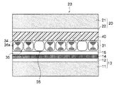
図1に本実施形態の光変調素子の一例の概略構成断面図を示すが、図にように、本実施形態の光変調素子10では、対向して設けられた一対の非表示面基板(基板)13と表示面基板(基板)20との間に、液晶ドロップ32及び樹脂スペーサー33を含む調光層30が設けられている。非表示面基板13は、支持基板11上に電極12を積層した構成となっている。表示面基板20は、支持基板21上に電極22を積層した構成となっている。非表示面基板13には遮光層14が設けられ、表示面基板20には調光層30が設けられており、接着層16を介して積層された構成となっている。
なお、図示は省略するが、電極22と調光層30との間、及び電極12と遮光層14との間等に接着層を設けてもよい。遮光層14は非表示面基板13の外側、即ち電極12が形成されていない側、あるいは表示面基板20側の電極22と調光層30との間に設けてられていてもよい。調光層30は、液晶32aを含む球状の液晶ドロップ32及び球状の樹脂スペーサー33が、ゼラチン(高分子バインダー)34中に配列した状態で構成されている。
FIG. 1 shows a schematic cross-sectional view of an example of the light modulation element of the present embodiment. As shown in the figure, in the
Although illustration is omitted, an adhesive layer may be provided between the
このように構成された光変調素子10において、対向する電極22及び電極12へ電圧が印加されると、印加電圧に応じてコレステリック液晶の配向状態が制御され、調光層30へ入射された入射光が、コレステリック液晶により選択反射される。
In the
なお、図1に示す光変調素子10の調光層30は、コレステリック液晶をドロップとしてではなく、液晶32aを高分子シェル、すなわち液晶マイクロカプセルに包み込んだ形態の液晶マイクロカプセルとして含むようにしてもよい。以下において、特に明記しない場合には「液晶ドロップ」というときには、その内容は前記液晶マイクロカプセルについても同様に適用される。
The
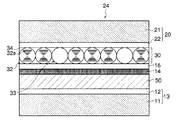
また本実施形態においては、図2に示すように樹脂スペーサー35が多角柱形状であることが望ましく、さらにこれに合わせて液晶36aを含む液晶ドロップ36も多角柱形状であることが望ましい。
樹脂スペーサー35が多角柱形状、特に六面体形状であると、図に示すように樹脂スペーサー35が電極を有する基板と面で接触することができ、スペーサーの配置が安定化され、またスペーサー導入による調光層面の凹凸の発生も抑制することができる。また、液晶ドロップ36も多角柱形状であることにより、同様に液晶ドロップ36も多角柱形状の樹脂スペーサー35と揃った状態で密に配列することができ、表示と強度との安定性がより高められる。
Further, in the present embodiment, as shown in FIG. 2, it is desirable that the
If the
ここで、上記「多角柱形状」とは、調光層面を500乃至1000倍程度で顕微鏡観察したときに、目視で液晶ドロップ等の粒子形状が円でなく、輪郭に2つ以上の角を有するものを意味する。またこのとき、例えばレーザー顕微鏡などにより焦点をずらして観察面と垂直方向の形状変化を調べ、同様の形状が深さ方向にも続いていることを確認することにより、多角柱形状であることが明確に判断される。
なお光変調素子において、樹脂スペーサー等が多角柱形状であるとは、観察される樹脂スペーサー粒子等全体の50個数%以上が多角柱形状であることをいう。
Here, the “polygonal column shape” means that when the light control layer surface is observed with a microscope at a magnification of about 500 to 1000 times, the particle shape such as a liquid crystal drop is not a circle and has two or more corners in the outline. Means things. Also, at this time, for example, by changing the focus with a laser microscope or the like and examining the shape change in the direction perpendicular to the observation surface, confirming that the same shape continues in the depth direction, it may be a polygonal column shape It is judged clearly.
In the light modulation element, the resin spacer or the like having a polygonal column shape means that 50% by number or more of the entire resin spacer particles or the like to be observed have a polygonal column shape.
さらに、前記樹脂スペーサーと液晶ドロップとがほぼ同サイズであることが望ましい。樹脂スペーサーと液晶ドロップとが同サイズであることにより、図2に示すように、例えば樹脂スペーサー35及び液晶ドロップ36が単層で配列したときに、より稠密な配置とすることができる。
Furthermore, it is desirable that the resin spacer and the liquid crystal drop have substantially the same size. Since the resin spacer and the liquid crystal drop are the same size, as shown in FIG. 2, for example, when the
ここで上記「ほぼ同サイズ」とは両粒子の最大長差が±50%以内であることを意味し、該最大長は、前記顕微鏡観察した調光層面の写真を画像解析し、液晶ドロップ粒子及び樹脂スペーサー粒子1000個以上各々について最大長を求め、それらの平均値の差として求められるものである。
また、前記「稠密な配置」とは、樹脂スペーサー及び液晶ドロップが互いに最大長の100%以上の間隙を空けることなく密に並列していることをいう。
Here, “substantially the same size” means that the maximum length difference between the two particles is within ± 50%, and the maximum length is obtained by image analysis of the photo of the light control layer surface observed by the microscope, and liquid crystal drop particles In addition, the maximum length is obtained for each of 1,000 or more resin spacer particles, and is obtained as a difference between the average values thereof.
The “dense arrangement” means that the resin spacers and the liquid crystal drops are closely arranged in parallel without leaving a gap of 100% or more of the maximum length.
本実施形態の光変調素子としては、調光層31上にさらに被覆層40を設けた図3に示した構成がさらに好適である。後述するように、前記樹脂スペーサー及び液晶ドロップが多角柱形状となるには、調光層塗布液の塗布を行って一度ゼラチンを固化させたのち、再度ゼラチンをゾル化して保持する工程が必要となる。このとき、ゾル化の前に調光層上にゲル化した膜(上記保持する工程の条件ではゾル化しない膜)である被覆層40を設けておくことにより、前記保持工程における多角柱形状化を効率的に行うことができる。
As the light modulation element of the present embodiment, the configuration shown in FIG. 3 in which a
また、上記被覆層40は、光変調素子作製の際に調光層31が外部に露出しないようにして、調光層31を保護する機能をも有しているため、作製時における調光層の乱れが抑制され、表示特性も向上する。
なお、本実施形態における前記「ゲル化した膜」とは、3次元的に水素結合して溶剤に不溶となった膜のことであり、超音波式粘度測定器により確認することができる。
The
The “gelled film” in the present embodiment is a film that is three-dimensionally hydrogen bonded and insoluble in a solvent, and can be confirmed by an ultrasonic viscosity measuring device.
さらに本実施形態において、例えば図1に示す光変調素子10は、図4に示すように、電極12と遮光層14との間に光導電層50を設けた構成の光変調素子24であってもよい。図4に示す光変調素子24によれば、電極12及び電極22の間にバイアス電圧を印加するとともに、光導電層50に書込み光を照射することによって、コレステリック液晶の配向状態を制御することができる。
Further, in the present embodiment, for example, the
なお、上記支持基板21及び支持基板11が、本実施形態における基板に相当し、液晶ドロップ32及び液晶マイクロカプセル36各々が、本実施形態における液晶ドロップ及び液晶マイクロカプセル各々に相当し、樹脂スペーサー33、35各々が本実施形態における樹脂スペーサーに相当する。また、上記電極12及び電極22各々が、本実施形態における電極に相当し、上記光変調素子10、光変調素子23、及び光変調素子24が、本実施形態における光変調素子に相当する。
The
次に、前記で説明した光変調素子に用いる各構成部材について説明する。
<基板>
基板を構成する支持基板は、絶縁性を有する、ガラス、及びシリコーン、またはポリエチレンテレフタレート、ポリスルホン、ポリエーテルスルホン、ポリカーボネートなどの高分子フィルムを用いて形成され、少なくとも一方、特に視認される側の支持基板(表示面基板を構成する支持基板)は、入射光及び反射光に対して透過性を有する材料により形成される。また必要に応じて、支持基板の表面に、防汚膜、耐磨耗膜、光反射防止膜、ガスバリア膜など公知の機能性膜を形成してもよい。
Next, each component used for the light modulation element described above will be described.
<Board>
The support substrate constituting the substrate is formed using glass and silicone or polymer films such as polyethylene terephthalate, polysulfone, polyethersulfone, polycarbonate, etc., which have insulating properties, and at least one of the supports that is particularly visible The substrate (supporting substrate constituting the display surface substrate) is formed of a material that is transmissive to incident light and reflected light. Moreover, you may form well-known functional films, such as a pollution protection film, an abrasion-resistant film | membrane, a light reflection prevention film, and a gas barrier film, on the surface of a support substrate as needed.
支持基板上に設けられる電極は、導電性を有する、金やアルミなどの金属薄膜、酸化インジウムや酸化スズなどの金属酸化物、またはポリピロール、ポリアセチレン、ポリアニリンなどの導電性有機高分子を用いて形成され、少なくとも表示面側にある電極は、入射光及び反射光に対して透過性を有する材料により形成する。また必要に応じて、その表面に、密着力改善膜、光反射防止膜、ガスバリア膜など公知の機能性膜を形成してもよい。 The electrode provided on the support substrate is formed using a conductive metal thin film such as gold or aluminum, a metal oxide such as indium oxide or tin oxide, or a conductive organic polymer such as polypyrrole, polyacetylene, or polyaniline. In addition, at least the electrode on the display surface side is formed of a material that is transmissive to incident light and reflected light. Moreover, you may form well-known functional films, such as an adhesive force improvement film | membrane, a light reflection prevention film | membrane, and a gas barrier film, on the surface as needed.
<調光層>
調光層は、液晶による液晶ドロップまたは液晶マイクロカプセルを、ゼラチン中に、分散保持した構造からなる。調光層の層厚は、大きすぎると電極間に印加する駆動電圧を高くする必要があり、小さすぎると光変調素子のコントラストが低下することから、駆動電圧を低く且つコントラストを高くするために、1μm以上100μm以下であることが好ましい。
本実施形態の光変調素子における調光層は、液晶ドロップまたは液晶マイクロカプセルが単層で構成されていても、複層で構成されていてもよいが、調光層の凹凸を抑制するために、単層であることが好ましい。
<Light control layer>
The light control layer has a structure in which liquid crystal drops or liquid crystal microcapsules made of liquid crystals are dispersed and held in gelatin. If the layer thickness of the light control layer is too large, it is necessary to increase the driving voltage applied between the electrodes. If the layer thickness is too small, the contrast of the light modulation element is lowered, so that the driving voltage is lowered and the contrast is increased. It is preferable that they are 1 micrometer or more and 100 micrometers or less.
The light control layer in the light modulation device of the present embodiment may be formed of a single layer or a plurality of liquid crystal drops or liquid crystal microcapsules, but in order to suppress unevenness of the light control layer A single layer is preferable.
(液晶)
調光層において、液晶ドロップや液晶マイクロカプセルに用いることができる液晶材料としては、屈折率異方性があり、電圧印加によって配向が変化するものであればどのような液晶材料であってもよいが、好ましくは、コレステリック液晶(カイラルネマチック液晶を含む)が挙げられる。
なお、本実施形態で用いられるコレステリック液晶材料として、ステロイド系コレステロール誘導体、あるいはシッフ塩基系、アゾ系、アゾキシ系、安息香酸エステル系、ビフェニル系、ターフェニル系、シクロヘキシルカルボン酸エステル系、フェニルシクロヘキサン系、ビフェニルシクロヘキサン系、ピリミジン系、ジオキサン系、シクロヘキシルシクロヘキサンエステル系、シクロヘキシルエタン系、シクロヘキサン系、トラン系、アルケニル系、スチルベン系、縮合多環系などのネマチック液晶やスメクチック液晶、またはこれらの混合液晶に、シッフ塩基系、アゾ系、エステル系、ビフェニル系などの光学活性材料からなるカイラル成分を添加した材料を用いることができる。
(liquid crystal)
As the liquid crystal material that can be used for the liquid crystal drop or the liquid crystal microcapsule in the light control layer, any liquid crystal material may be used as long as it has refractive index anisotropy and the orientation is changed by voltage application. However, cholesteric liquid crystals (including chiral nematic liquid crystals) are preferable.
The cholesteric liquid crystal material used in this embodiment is a steroid cholesterol derivative, or a Schiff base, azo, azoxy, benzoate, biphenyl, terphenyl, cyclohexylcarboxylate, or phenylcyclohexane. , Biphenylcyclohexane, pyrimidine, dioxane, cyclohexylcyclohexane ester, cyclohexylethane, cyclohexane, tolan, alkenyl, stilbene, condensed polycyclic nematic liquid crystals, smectic liquid crystals, or mixed liquid crystals thereof A material to which a chiral component made of an optically active material such as Schiff base, azo, ester, or biphenyl is added can be used.
(樹脂スペーサー)
また、調光層において樹脂スペーサーとしては硬化性樹脂が好適に用いられる。
硬化性樹脂としては光硬化性、放射線硬化性、電子線硬化性、熱硬化性等の樹脂を用いることができるが、中でも光硬化性樹脂及び熱硬化性樹脂が好ましく用いられる。該光硬化性樹脂または熱硬化性樹脂としては、光硬化性または熱硬化性のモノマー、オリゴマー若しくはモノマーとオリゴマーの混合物が好ましく用いられる。なお、本実施形態に用いる硬化性樹脂としては、後述する乳化工程を経て調光層用塗布液に分散されるため、水溶性でないことが望ましい。
(Resin spacer)
In the light control layer, a curable resin is preferably used as the resin spacer.
As the curable resin, a photocurable resin, a radiation curable resin, an electron beam curable resin, a thermosetting resin, or the like can be used. Among them, a photocurable resin and a thermosetting resin are preferably used. As the photocurable resin or thermosetting resin, a photocurable or thermosetting monomer, an oligomer, or a mixture of a monomer and an oligomer is preferably used. In addition, as curable resin used for this embodiment, since it disperse | distributes to the coating liquid for light control layers through the emulsification process mentioned later, it is desirable that it is not water-soluble.
前記熱硬化性樹脂としては、加熱すると硬化(不溶化)する樹脂として知られているものを適用できる。例えば、フェノール−ホルムアルデヒド樹脂、尿素−ホルムアルデヒド樹脂、メラミン−ホルムアルデヒド樹脂、アクリルポリオールをイソシアネートで硬化させた樹脂、ポリエステルポリオールをメラミンで硬化させた樹脂、あるいはアクリル酸をメラミンで硬化させた樹脂等である。また熱硬化性樹脂の構成成分であるモノマーを組み合わせて用いてもよい。 As said thermosetting resin, what is known as resin hardened | cured (insolubilized) when heated can be applied. For example, phenol-formaldehyde resin, urea-formaldehyde resin, melamine-formaldehyde resin, resin obtained by curing acrylic polyol with isocyanate, resin obtained by curing polyester polyol with melamine, or resin obtained by curing acrylic acid with melamine . Moreover, you may use combining the monomer which is a structural component of a thermosetting resin.
その他に熱可塑性樹脂でも架橋によって硬化し耐熱性を有する樹脂であれば、前記熱硬化性樹脂に含まれる。このような熱硬化性樹脂としては、例えば、熱硬化性アクリル樹脂を使用することが好ましい。熱硬化性アクリル樹脂は、少なくとも1種のアクリル系単量体、あるいはアクリル系単量体及びスチレン系単量体を重合してなる共重合体をメラミン系化合物、イソシアネート系化合物によって架橋させたものである。さらに、熱硬化性シリコーン樹脂も好ましい。
これらの中では、熱硬化性シリコーン樹脂を特に好適に用いることができる。
In addition, any thermoplastic resin that is cured by crosslinking and has heat resistance is included in the thermosetting resin. As such a thermosetting resin, for example, a thermosetting acrylic resin is preferably used. Thermosetting acrylic resin is obtained by crosslinking at least one acrylic monomer or a copolymer obtained by polymerizing acrylic monomer and styrene monomer with melamine compound or isocyanate compound. It is. Furthermore, a thermosetting silicone resin is also preferable.
In these, a thermosetting silicone resin can be used especially suitably.
前記光硬化性樹脂組成物としては、例えば、分子中にビニル基等の反応性二重結合を有する化合物(低分子量物に限らず、高分子をも含むものとする)と、光硬化に必要な開始剤と、を主成分とするもの等が挙げられる。
上記分子中に反応性二重結合を有する化合物としては、(メタ)アクリロイル基を有する、例えば、メチル(メタ)アクリレート、エチル(メタ)アクリレート、ベンジル(メタ)アクリレート、2−エトキシエチル(メタ)アクリレート、フェノキシジエチレングリコール(メタ)アクリレートなどの1官能タイプや、1,6−ヘキサンジオールジ(メタ)アクリレート、ネオペンチルグリコールジ(メタ)アクリレート、ポリエチレングリコールジ(メタ)アクリレート、ポリプロピレングリコールジ(メタ)アクリレート、トリメチルプロパントリ(メタ)アクリレート、ペンタエリスリトールトリ(メタ)アクリレート、ペンタエリスリトールテトラ(メタ)アクリレート、ジペンタエリスリトールヘキサ(メタ)アクリレート等の多官能タイプがある。また、ポリエステルアクリレート、ポリウレタンアクリレート、エポキシアクリレート、ポリエーテルアクリレート、オリゴアクリレート、アルキドアクリレート、ポリオールアクリレート等のオリゴマー等もある。更に、ビニル基やアリル基を有する、例えば、スチレンモノマー、α−メチルスチレン、ジビニルベンゼン、酢酸ビニル、ペンテン、ヘキセン、不飽和化合物等がある。さらに、チオール系の重合性単量体やエポキシ系の重合性単量体なども有効である。
光硬化用重合開始剤としては、例えば、ベンゾインアルキルエーテル系、アセトフェノン系、ベンゾフェノン系、チオキサントン系などの光開始剤が好適に用いられる。
Examples of the photocurable resin composition include a compound having a reactive double bond such as a vinyl group in a molecule (not only a low molecular weight substance but also a polymer), and a start necessary for photocuring. And the like mainly containing an agent.
Examples of the compound having a reactive double bond in the molecule include a (meth) acryloyl group, such as methyl (meth) acrylate, ethyl (meth) acrylate, benzyl (meth) acrylate, and 2-ethoxyethyl (meth). Monofunctional type such as acrylate, phenoxydiethylene glycol (meth) acrylate, 1,6-hexanediol di (meth) acrylate, neopentyl glycol di (meth) acrylate, polyethylene glycol di (meth) acrylate, polypropylene glycol di (meth) Acrylate, trimethylpropane tri (meth) acrylate, pentaerythritol tri (meth) acrylate, pentaerythritol tetra (meth) acrylate, dipentaerythritol hexa (meth) acrylate, etc. There is a functional type. Further, there are oligomers such as polyester acrylate, polyurethane acrylate, epoxy acrylate, polyether acrylate, oligo acrylate, alkyd acrylate, polyol acrylate and the like. Furthermore, there are, for example, styrene monomer, α-methylstyrene, divinylbenzene, vinyl acetate, pentene, hexene and unsaturated compounds having a vinyl group or an allyl group. Furthermore, thiol polymerizable monomers and epoxy polymerizable monomers are also effective.
As the photocuring polymerization initiator, for example, benzoin alkyl ether-based, acetophenone-based, benzophenone-based, thioxanthone-based photoinitiators are preferably used.
これらの硬化性樹脂としては、後述する調光層形成工程における加熱等により硬化時期が制限されないことが望ましく、その観点からは、光照射により硬化時期を任意とできる光硬化性樹脂を用いることが好適である。
特に樹脂スペーサーとして、表示特性に悪影響を与えないという点では用いる液晶と屈折率が近いことが望ましく、例えば、紫外線硬化性のチオール系重合性単量体であるNOA65(ノーランド社製)等が好ましい。
As these curable resins, it is desirable that the curing time is not limited by heating or the like in the light control layer forming step described later, and from this viewpoint, a photocurable resin that can be arbitrarily cured by light irradiation is used. Is preferred.
In particular, as a resin spacer, it is desirable that the refractive index is close to the liquid crystal used in that it does not adversely affect the display characteristics. For example, NOA65 (manufactured by Norland), which is an ultraviolet curable thiol polymerizable monomer, is preferable. .
本実施形態に用いられる調光層において、樹脂スペーサー濃度(液晶ドロップ及び樹脂スペーサー全体体積に対する樹脂スペーサー体積比率)は、0.01体積%以上10体積%以下とすることが望ましく、0.5体積%以上2.0体積%以下とすることがより好適である。
体積比率が0.01体積%に満たないと、外部からの押圧等に対して表示特性に影響が出ない程度の強度を確保することができない場合がある。10体積%を超えると、反射率低下など表示特性に悪影響が出る場合がある。
In the light control layer used in this embodiment, the resin spacer concentration (resin spacer volume ratio with respect to the total volume of the liquid crystal drop and the resin spacer) is desirably 0.01 volume% or more and 10 volume% or less, and 0.5 volume. % To 2.0% by volume is more preferable.
If the volume ratio is less than 0.01% by volume, it may not be possible to secure a strength that does not affect the display characteristics against external pressure or the like. If it exceeds 10% by volume, display characteristics such as a decrease in reflectance may be adversely affected.
なお上記体積比率は、調光層表面の顕微鏡による観察写真から、1000個以上の粒子について画像データを画像解析装置に取り込み、各粒子ごとに最大径を測定し、それを直径とした球体の粒子の体積として液晶ドロップ及び樹脂スペーサーの各総体積を求めることにより行った。 Note that the volume ratio is obtained by taking image data of 1000 or more particles from an observation photograph with a microscope on the surface of the light control layer, measuring the maximum diameter of each particle, and measuring the maximum diameter of each particle as a spherical particle. The total volume of the liquid crystal drop and the resin spacer was determined as the volume of.
(高分子バインダー)
本実施形態における高分子バインダーは、前記液晶ドロップまたは液晶マイクロカプセルを保持し、光変調素子の変形による液晶ドロップまたは液晶マイクロカプセルの流動を抑制する。高分子バインダーは、液晶材料に溶解せず、また液晶ドロップまたは液晶マイクロカプセルと相溶しない液体を溶剤とする高分子材料であり、且つ外力に耐えうる強度を持ち、少なくとも反射光及び入射光に対して高い透過性を有する材料であれば特に制限はなく、例えば、水溶性高分子材料(たとえばゼラチン、ポリビニルアルコール、セルロース誘導体、ポリアクリル酸系ポリマー、エチレンイミン、ポリエチレンオキサイド、ポリアクリルアミド、ポリスチレンスルホン酸塩、ポリアミジン、イソプレン系スルホン酸ポリマー)、あるいは水性エマルジョン化できる材料(たとえばフッ素樹脂、シリコーン樹脂、アクリル樹脂、ウレタン樹脂、エポキシ樹脂)等が好適に挙げられる。
中でも、表面凹凸を小さくでき、フラットな調光層が得られるという観点から、ゼラチンが特に好ましい
(Polymer binder)
The polymer binder in the present embodiment holds the liquid crystal drop or liquid crystal microcapsule and suppresses the flow of the liquid crystal drop or liquid crystal microcapsule due to deformation of the light modulation element. The polymer binder is a polymer material that uses a liquid that does not dissolve in the liquid crystal material and is incompatible with the liquid crystal drop or the liquid crystal microcapsule, and has a strength that can withstand external force, and at least reflects light and incident light. The material is not particularly limited as long as the material has high permeability. For example, a water-soluble polymer material (for example, gelatin, polyvinyl alcohol, cellulose derivative, polyacrylic acid polymer, ethyleneimine, polyethylene oxide, polyacrylamide, polystyrene sulfone). Preferable examples include acid salts, polyamidines, isoprene-based sulfonic acid polymers), and materials that can be emulsified in water (for example, fluorine resins, silicone resins, acrylic resins, urethane resins, and epoxy resins).
Among these, gelatin is particularly preferable from the viewpoint that the surface unevenness can be reduced and a flat light control layer can be obtained.
前記ゼラチンとしては、ゼラチンの物性として、ゼリー強度が大きく、ゾル粘度が低いものが好ましい。
このようなゼラチンとしては、α鎖の多量体である高分子量のβ鎖・γ鎖や、α鎖の主鎖が途中で切れた低分子量成分が少なく、α鎖残量の多いものが適している。牛骨を酸処理して製造されたゼラチン材料は、この条件を満たし、とくにゼリー強度が大きく、ゾル粘度が低いため好ましい。また、原料のコラーゲンを加水分解する際に最初に抽出される第一抽出品がよい。なお、液晶材料のイオン汚染を防止するため、ゼラチン中に残留するイオン成分をイオン交換樹脂など公知の手法を用いて除去してもよい。
As the gelatin, gelatin having a high jelly strength and a low sol viscosity is preferable.
As such gelatin, those having a high molecular weight β chain / γ chain, which is a polymer of α chains, and low molecular weight components in which the main chain of the α chain is cut off in the middle and having a large α chain remaining amount are suitable. Yes. A gelatin material produced by acid treatment of bovine bone is preferable because it satisfies this condition, and particularly has high jelly strength and low sol viscosity. Moreover, the 1st extract extracted first when hydrolyzing the collagen of a raw material is good. In order to prevent ionic contamination of the liquid crystal material, ionic components remaining in the gelatin may be removed using a known technique such as an ion exchange resin.
<被覆層>
被覆層としては前記のようにゲル化した膜(ゲル化膜)が用いられる。ゲル化膜としては、温度によりゾル−ゲル状態を示し、ゲル化状態で液晶ドロップ等を溶解しない特性を有するものであれば特に制限されない。なお本実施形態において、「ゲル化する」および「ゲル状態になる」とは、ゲル状態での飽和粘度を100、ゾル状態での飽和粘度を0として規格化した場合に、上記規格化した粘度が70以上になった場合を意味する。
<Coating layer>
As the coating layer, a gelled film (gelated film) as described above is used. The gelled film is not particularly limited as long as it shows a sol-gel state depending on the temperature and has a property of not dissolving a liquid crystal drop or the like in the gelled state. In this embodiment, “gelate” and “become in a gel state” mean that when the saturated viscosity in a gel state is 100 and the saturated viscosity in a sol state is 0, the normalized viscosity Means that the value becomes 70 or more.
前記ゲル化膜のもととなるコロイド粒子としては、天然高分子、合成高分子、または半合成高分子を用いることができ、寒天、ゼラチン、セルロース、カラーギナン、アルギン酸、キサンタンガム、ペクチン、シードガム、ファーセレラン、カードラン、ポリビニルアルコール、ポリアクリロニトリル、ポリエチレンオキシド等の高分子やその誘導体、あるいはこれらの混合物、あるいはこれらを低温ゲル化剤として、低温ゲル化性の無い高分子と混合したものを例示することができる。中でも、温度変化に対するゾル−ゲル変化挙動に大きなヒステリシス性を示す寒天やその誘導体が好ましい。また高分子溶液の物性としては、ゼリー強度が大きく、ゾル粘度が低いものが好ましい。 As the colloidal particles that form the gelled film, natural polymer, synthetic polymer, or semi-synthetic polymer can be used, and agar, gelatin, cellulose, carrageenan, alginic acid, xanthan gum, pectin, seed gum, and far celeran. Exemplifying polymers such as curdlan, polyvinyl alcohol, polyacrylonitrile, polyethylene oxide and derivatives thereof, or mixtures thereof, or those mixed with polymers having no low-temperature gelation properties as a low-temperature gelling agent Can do. Of these, agar and its derivatives exhibiting large hysteresis in the sol-gel change behavior with respect to temperature change are preferable. As the physical properties of the polymer solution, those having high jelly strength and low sol viscosity are preferred.
被覆層の層厚は、0.1μm以上5.0μm以下であることが望ましく、0.5μm以上2.0μm以下がより好適である。層厚が5.0μmを超えると、ゲル化膜での電圧降下が大きくなるため駆動電圧の上昇を引き起こすという問題が生じ、0.1μm未満であると、調光層の表面を充分被覆できず液晶ドロップや樹脂スペーサーの形状が不均一になったり液晶の拡散を抑制することができなかったりする場合がある。 The thickness of the coating layer is desirably 0.1 μm or more and 5.0 μm or less, and more preferably 0.5 μm or more and 2.0 μm or less. If the layer thickness exceeds 5.0 μm, the voltage drop at the gelled film increases, causing a problem of increasing the drive voltage. If the layer thickness is less than 0.1 μm, the surface of the light control layer cannot be sufficiently covered. There are cases where the shape of the liquid crystal drop or the resin spacer becomes non-uniform or the diffusion of the liquid crystal cannot be suppressed.
<光導電層>
光導電層は、a−Si:H、a−Se、Te−Se、As2Se3、CdSe、CdS
などの無機光導電体、あるいはアゾ顔料、フタロシアニン顔料、ペリレン顔料、キナクリドン顔料、ピロロピロール顔料、インジゴ顔料、アントロン顔料などの電荷発生材料とアリールアミン、ヒドラゾン、トリフェニルメタン、PVKなどの電荷輸送材料を組合せた有機光導電体(OPC)などにより構成されるが、2つの電荷発生層及び電荷輸送層が積層されたOPC層が好ましい。
<Photoconductive layer>
The photoconductive layer is composed of a-Si: H, a-Se, Te-Se, As 2 Se 3 , CdSe, CdS.
Inorganic photoconductors such as azo pigments, phthalocyanine pigments, perylene pigments, quinacridone pigments, pyrrolopyrrole pigments, indigo pigments, anthrone pigments, and charge transport materials such as arylamines, hydrazones, triphenylmethane, and PVK The organic photoconductor (OPC) is a combination of the two, and an OPC layer in which two charge generation layers and a charge transport layer are stacked is preferable.
電荷発生層は、アドレス光を吸収して光キャリアを発生させる機能を有する層である。主に、電荷発生層が表示面側の電極から書き込み面側の電極の方向に流れる光キャリア量を、電荷発生層が書き込み面側の電極から表示面側の電極の方向に流れる光キャリア量を、それぞれ左右している。電荷発生層としては、アドレス光を吸収して励起子を発生させ、CGL内部、またはCGL/CTL界面で自由キャリアに効率良く分離させられるものが好ましい。 The charge generation layer is a layer having a function of absorbing address light and generating photocarriers. Mainly, the amount of light carriers that the charge generation layer flows from the electrode on the display surface side to the electrode on the writing surface side, and the amount of light carriers that the charge generation layer flows from the electrode on the writing surface side to the electrode on the display surface side. , Each has an influence. The charge generation layer is preferably one that absorbs address light to generate excitons and can be efficiently separated into free carriers within the CGL or at the CGL / CTL interface.
電荷発生層は、電荷発生材料(たとえば金属又は無金属フタロシアニン、スクアリウム化合物、アズレニウム化合物、ペリレン顔料、インジゴ顔料、ビスやトリス等アゾ顔料、キナクリドン顔料、ピロロピロール色素、多環キノン顔料、ジブロモアントアントロンなど縮環芳香族系顔料、シアニン色素、キサンテン顔料、ポリビニルカルバゾールとニトロフルオレン等電荷移動錯体、ピリリウム塩染料とポリカーボネート樹脂からなる共昌錯体)を直接成膜する乾式法か、またはこれら電荷発生材料を、高分子バインダー(たとえばポリビニルブチラール樹脂、ポリアリレート樹脂、ポリエステル樹脂、フェノール樹脂、ビニルカルバゾール樹脂、ビニルホルマール樹脂、部分変性ビニルアセタール樹脂、カーボネート樹脂、アクリル樹脂、塩化ビニル樹脂、スチレン樹脂、ビニルアセテート樹脂、酢酸ビニル樹脂、シリコーン樹脂等)とともに適当な溶剤に分散ないし溶解させて塗布液を調製し、これを塗布し乾燥させて成膜する湿式塗布法等により形成することができる。 The charge generation layer is formed of a charge generation material (for example, metal or metal-free phthalocyanine, squalium compound, azurenium compound, perylene pigment, indigo pigment, azo pigment such as bis and tris, quinacridone pigment, pyrrolopyrrole dye, polycyclic quinone pigment, dibromoanthanthrone. Such as fused-ring aromatic pigments, cyanine dyes, xanthene pigments, charge transfer complexes such as polyvinylcarbazole and nitrofluorene, kyosho complexes composed of pyrylium salt dyes and polycarbonate resins), or these charge generation materials A polymer binder (for example, polyvinyl butyral resin, polyarylate resin, polyester resin, phenol resin, vinyl carbazole resin, vinyl formal resin, partially modified vinyl acetal resin, carbonate resin, acrylic resin, A coating solution prepared by dispersing or dissolving it in an appropriate solvent together with a vinyl chloride resin, a styrene resin, a vinyl acetate resin, a vinyl acetate resin, a silicone resin, etc.) Can be formed.
電荷輸送層は、電荷発生層で発生した光キャリアが注入さ、バイアス信号で印加された電場方向にドリフトする機能を有する層である。
電荷輸送層は、電荷発生層からの自由キャリアの注入が効率良く発生し(電荷発生層23,25とイオン化ポテンシャルが近いことが好ましい)、注入された自由キャリアができるだけ高速にホッピング移動するものが好適である。暗時のインピーダンスを高くするため、熱キャリアによる暗電流は低い方が好ましい。
The charge transport layer is a layer having a function of drifting in the direction of an electric field applied with a bias signal when photocarriers generated in the charge generation layer are injected.
In the charge transport layer, free carriers are efficiently injected from the charge generation layer (preferably close to the ionization potential of the charge generation layers 23 and 25), and the injected free carriers hop and move as fast as possible. Is preferred. In order to increase the dark impedance, it is preferable that the dark current due to the heat carrier is low.
電荷輸送層は、低分子の正孔輸送材料(たとえばトリニトロフルオレン系化合物、ポリビニルカルバゾール系化合物、オキサジアゾール系化合物、ベンジルアミノ系ヒドラゾンあるいはキノリン系ヒドラゾン等のヒドラゾン系化合物、スチルベン系化合物、トリフェニルアミン系化合物、トリフェニルメタン系化合物、ベンジジン系化合物)、または低分子の電子輸送材料(たとえばキノン系化合物、テトラシアノキノジメタン系化合物、フルフレオン化合物、キサントン系化合物、ベンゾフェノン系化合物)を、高分子バインダー(たとえばポリカーボネート樹脂、ポリアリレート樹脂、ポリエステル樹脂、ポリイミド樹脂、ポリアミド樹脂、ポリスチレン樹脂、含珪素架橋型樹脂等)とともに適当な溶剤に分散ないし溶解させたもの、あるいは上記正孔輸送材料や電子輸送材料を高分子化した材料を適当な溶剤に分散ないし溶解させたものを調製し、これを塗布し乾燥させて形成すればよい。 The charge transport layer comprises a low molecular weight hole transport material (for example, trinitrofluorene compound, polyvinylcarbazole compound, oxadiazole compound, hydrazone compound such as benzylamino hydrazone or quinoline hydrazone, stilbene compound, Phenylamine compounds, triphenylmethane compounds, benzidine compounds), or low molecular electron transport materials (for example, quinone compounds, tetracyanoquinodimethane compounds, furfreon compounds, xanthone compounds, benzophenone compounds) Dispersed or dissolved in an appropriate solvent together with a polymer binder (for example, polycarbonate resin, polyarylate resin, polyester resin, polyimide resin, polyamide resin, polystyrene resin, silicon-containing crosslinked resin, etc.) There may be formed by the hole transporting material and electron transport material were prepared are dispersed or dissolved in a suitable solvent polymerized material, then it was applied and dried.
<遮光層>
必要に応じて設けられる遮光層は、絶縁性を有する、カドミウム系、クロム系、コバルト系、マンガン系、カーボン系などの無機顔料、またはアゾ系、アントラキノン系、インジゴ系、トリフェニルメタン系、ニトロ系、フタロシアニン系、ペリレン系、ピロロピロール系、キナクリドン系、多環キノン系、スクエアリウム系、アズレニウム系、シアニン系、ピリリウム系、アントロン系などの有機染料や有機顔料、あるいはこれらを高分子バインダーに分散した材料を用いて形成され、少なくとも反射光に対して、光吸収性を有するように構成する。
<Light shielding layer>
The light shielding layer provided as necessary is an insulating cadmium-based, chromium-based, cobalt-based, manganese-based, carbon-based inorganic pigment, or azo-based, anthraquinone-based, indigo-based, triphenylmethane-based, nitro-based , Phthalocyanine, perylene, pyrrolopyrrole, quinacridone, polycyclic quinone, squalium, azurenium, cyanine, pyrylium, anthrone organic dyes and pigments, or these as polymer binders It is formed using a dispersed material, and is configured to have light absorptivity with respect to at least reflected light.
<接着層>
必要に応じて設けられる接着層は、ウレタン樹脂、エポキシ樹脂、アクリル樹脂、シリコーン樹脂など、熱や圧力によって調光層と遮光層を密着させることができる材料を用いる。なお、接着層を挿入する位置はこの実施形態に限らず、電極と調光層の間、電極と遮光層の間とすることもできる。電極と調光層の間に接着層を形成する場合は、少なくとも入射光及び反射光に対して透過性を有する材料により形成する。
<Adhesive layer>
The adhesive layer provided as necessary uses a material that can adhere the light control layer and the light shielding layer by heat or pressure, such as urethane resin, epoxy resin, acrylic resin, or silicone resin. The position where the adhesive layer is inserted is not limited to this embodiment, and may be between the electrode and the light control layer, or between the electrode and the light shielding layer. In the case where an adhesive layer is formed between the electrode and the light control layer, the adhesive layer is formed of a material having transparency to at least incident light and reflected light.
次に、本実施形態の光変調素子の作製方法について説明する。なおここでは、説明を簡略化するために、図1、図2に示すように、対向して設けられた非表示面基板と表示面基板との間に、液晶ドロップを含む調光層が設けられる場合を説明する。 Next, a method for manufacturing the light modulation element of this embodiment will be described. Here, in order to simplify the explanation, as shown in FIGS. 1 and 2, a light control layer including a liquid crystal drop is provided between the non-display surface substrate and the display surface substrate which are provided to face each other. The case where it is possible will be described.
本実施形態の光変調素子は、例えば表面に電極を有する支持基板としての非表示面基板上に遮光層を積層し、また、表面に電極を有する支持基板としての表示面基板上に調光層を積層した後に、接着層を介して、表面に電極を有する支持基板としての表示面基板を電極が形成された側と表面に電極を有する支持基板としての非表示面基板の電極が形成された面とが対向するように重ね合わせて接着することにより作製される。 In the light modulation element of the present embodiment, for example, a light shielding layer is laminated on a non-display surface substrate as a support substrate having electrodes on the surface, and a light control layer is provided on the display surface substrate as a support substrate having electrodes on the surface. After stacking, the electrode of the non-display surface substrate as the support substrate having the electrode on the side where the electrode was formed and the display surface substrate as the support substrate having the electrode on the surface were formed through the adhesive layer It is manufactured by overlapping and adhering so that the surfaces face each other.
前記本実施形態の光変調素子は、特に調光層形成工程で樹脂スペーサーとなる硬化性樹脂滴を混入させたり、液滴を変形させたりすることによって得られるものである、この調光層形成工程を中心に説明する。また、調光層に用いる高分子バインダーとしては、好適な材料であるゼラチンを用いた形態とする。 The light modulation element of the present embodiment is obtained by mixing a curable resin droplet that becomes a resin spacer in the light control layer forming step, or by deforming the liquid droplet. The process will be mainly described. The polymer binder used for the light control layer is a form using gelatin which is a suitable material.
本実施形態において、調光層を設ける工程は、表示面基板上に、ゼラチン及び溶媒を含む溶液中に液晶ドロップまたは液晶マイクロカプセル及び硬化性樹脂滴が分散された調光層用塗布液を塗布する塗布工程と、塗布された調光層用塗布液によって形成された塗布層を、ゼラチンの凝固点より高い温度で且つ溶媒の飽和蒸気圧と同一または溶媒の飽和蒸気圧に近い雰囲気中に所定時間保持する保持工程と、塗布層中の前記溶媒をゼラチンの凝固点以下の温度で揮発させて乾燥させる乾燥工程と、を有している。
本実施形態において、調光層の形成は、塗布として(1)調光層形成用塗布液の塗布工程のみを行う方法と、(2)前記塗布工程に加えて被覆層を形成する被覆層形成工程を行う方法と、に分けられる。
In this embodiment, the step of providing the light control layer is performed by applying a light control layer coating liquid in which liquid crystal drops or liquid crystal microcapsules and curable resin droplets are dispersed in a solution containing gelatin and a solvent on the display surface substrate. And a coating layer formed by the coated light control layer coating solution at a temperature higher than the freezing point of gelatin and the same as or near the saturated vapor pressure of the solvent for a predetermined time. A holding step of holding, and a drying step of evaporating the solvent in the coating layer at a temperature below the freezing point of gelatin and drying.
In the present embodiment, the light control layer is formed by applying (1) a method of performing only the coating process of the light control layer forming coating solution, and (2) forming a coating layer that forms a coating layer in addition to the coating process. And the method of performing the process.
A.調光層用塗布液の塗布工程のみを行う場合
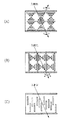
図5は、調光層の形成を調光層用塗布液の塗布工程のみにより行う場合を示す概略工程図である。
この方法による調光層形成は、調光層用塗布液を塗布する工程(工程(A1))、塗布した層を一定温度で保持する工程(工程(A2、A3)、及び乾燥する工程(工程(A4)から構成される。
A. FIG. 5 is a schematic process diagram showing a case where the light control layer is formed only by the application process of the light control layer coating liquid.
The light control layer formation by this method is a step of applying a light control layer coating liquid (step (A1)), a step of holding the applied layer at a constant temperature (steps (A2, A3)), and a step of drying (step). (A4).
(調光層用塗布液の調製)
まず調光層塗布に用いる調光層用塗布液の調製について詳細に説明する。
調光層用塗布液は、例えばゼラチン及び液体を含有する溶液に、液晶ドロップまたは液晶マイクロカプセルと、樹脂スペーサーとなる硬化性樹脂滴とを分散することによって調製される。
以下、液晶ドロップ及び液晶マイクロカプセルの調製方法について説明する。
(Preparation of coating solution for light control layer)
First, preparation of the light control layer coating solution used for light control layer application will be described in detail.
The light control layer coating solution is prepared, for example, by dispersing liquid crystal drops or liquid crystal microcapsules and curable resin droplets serving as resin spacers in a solution containing gelatin and a liquid.
Hereinafter, a method for preparing a liquid crystal drop and a liquid crystal microcapsule will be described.
−液晶ドロップエマルジョンの調製−
液晶ドロップエマルジョンは、少なくともコレステリック液晶からなる分散相を、分散相と相溶しない連続相、例えば、水相中にドロップ状に乳化分散させることにより調製される。乳化する手段として、分散相と連続相を混合した後、ホモジナイザーなどの機械的なせん断力で分散相を微小な液滴として分散させる方法や、分散相を連続相中に多孔質膜を通して押出し、微小な液滴として分散させる膜乳化法などを用いることができる。特に膜乳化法は乳化液滴の粒径ばらつきが小さくなるため、均一な粒径の液晶ドロップを形成することができるため好ましい。なお、乳化時の連続相中に、乳化を安定させるための界面活性剤や保護コロイドを微量混合しておいてもよい。
-Preparation of liquid crystal drop emulsion-
The liquid crystal drop emulsion is prepared by emulsifying and dispersing a dispersed phase composed of at least a cholesteric liquid crystal in a continuous phase incompatible with the dispersed phase, for example, an aqueous phase. As a means for emulsification, after mixing the dispersed phase and the continuous phase, a method of dispersing the dispersed phase as fine droplets by mechanical shearing force such as a homogenizer, or extruding the dispersed phase through the porous film in the continuous phase, For example, a film emulsification method in which fine droplets are dispersed can be used. In particular, the membrane emulsification method is preferable because liquid crystal drops having a uniform particle diameter can be formed because the dispersion of the particle diameters of the emulsified droplets is small. A small amount of a surfactant or protective colloid for stabilizing the emulsification may be mixed in the continuous phase during emulsification.
−液晶マイクロカプセルスラリーの調製−
高分子シェル内にコレステリック液晶が内包された液晶マイクロカプセルの調製には、公知の液晶マイクロカプセル化手法、例えば、相分離法、界面重合法、in situ重合法を用いることができる。具体的には、前記のごとくして作製した液晶ドロップを、高分子シェル材料を含む溶液中に分散させ、または前記材料に応じて熱硬化などさせ、液晶ドロップの周囲に高分子シェルを形成する。また、ウレタン・ウレア系の高分子シェルを作る場合には、あらかじめ液晶ドロップに多価イソシアネート化合物を含ませておき、液晶ドロップを、多価アルコールを含む溶液中に添加してウレタン・ウレア生成反応を起こさせることが好ましい。
-Preparation of liquid crystal microcapsule slurry-
In preparing a liquid crystal microcapsule in which a cholesteric liquid crystal is encapsulated in a polymer shell, a known liquid crystal microencapsulation method such as a phase separation method, an interfacial polymerization method, or an in situ polymerization method can be used. Specifically, the liquid crystal drop produced as described above is dispersed in a solution containing a polymer shell material, or is thermoset according to the material to form a polymer shell around the liquid crystal drop. . Also, when making urethane / urea polymer shells, a polyisocyanate compound is added to the liquid crystal drop in advance, and the liquid crystal drop is added to a solution containing the polyhydric alcohol to generate a urethane / urea reaction. It is preferable to cause
高分子シェルとしては内包する液晶材料に溶解しない材料を用い、例えば、ゼラチン、セルロース誘導体、ゼラチン−アラビアゴム、ゼラチン−ゲランゴム、ゼラチン−ペプトン、ゼラチン−カルボキシメチルセルロース、ポリスチレン、ポリアミド、ナイロン、ポリエステル、ポリフェニルエステル、ポリウレタン、ポリウレア、メラミンホルマリン樹脂、フェノールホルマリン樹脂、尿素ホルマリン樹脂、アクリル樹脂、メタクリル樹脂などが挙げられる。 As the polymer shell, a material that does not dissolve in the encapsulated liquid crystal material is used. For example, gelatin, cellulose derivative, gelatin-gum arabic, gelatin-gellan gum, gelatin-peptone, gelatin-carboxymethylcellulose, polystyrene, polyamide, nylon, polyester, poly Examples include phenyl ester, polyurethane, polyurea, melamine formalin resin, phenol formalin resin, urea formalin resin, acrylic resin, and methacrylic resin.
液晶マイクロカプセルの粒径は小さすぎると充分な反射特性が得られず、表示特性を悪化させると共に、コントラストの低下を招く。一方、高分子シェルによる液晶マイクロカプセルの壁厚は、厚すぎると液晶マイクロカプセル内に内包される液晶材料の量が少なくなり、薄すぎると強度が低下する。したがって、コントラストが高く且つ強度の低下を抑制するには、液晶マイクロカプセルの壁厚は、液晶マイクロカプセルの半径の1%乃至25%、好ましくは3%乃至21%にする。 If the particle size of the liquid crystal microcapsules is too small, sufficient reflection characteristics cannot be obtained, which deteriorates display characteristics and lowers contrast. On the other hand, if the wall thickness of the liquid crystal microcapsule by the polymer shell is too thick, the amount of the liquid crystal material included in the liquid crystal microcapsule decreases, and if it is too thin, the strength decreases. Therefore, in order to suppress the decrease in strength with high contrast, the wall thickness of the liquid crystal microcapsule is set to 1% to 25%, preferably 3% to 21%, of the radius of the liquid crystal microcapsule.
なお、液晶マイクロカプセル及び液晶ドロップの体積平均一次粒径は、1μm以上100μm以下が好ましく、3μm以上20μm以下がより好ましく、特に好ましくは10μm以上15μm以下である。液晶マイクロカプセル及び液晶ドロップの体積平均一次粒径が100μmを超えると駆動電圧の上昇を生じ、1μm未満であると充分な反射特性が期待できないおそれがある。
ただし、この段階で液晶ドロップ等の粒径は、調光層用塗布液として混合される硬化性樹脂滴の粒径とほぼ同一としておくことが望ましい。
The volume average primary particle size of the liquid crystal microcapsules and the liquid crystal drop is preferably 1 μm or more and 100 μm or less, more preferably 3 μm or more and 20 μm or less, and particularly preferably 10 μm or more and 15 μm or less. If the volume average primary particle size of the liquid crystal microcapsules and the liquid crystal drop exceeds 100 μm, the drive voltage increases, and if it is less than 1 μm, sufficient reflection characteristics may not be expected.
However, at this stage, it is desirable that the particle size of the liquid crystal drop or the like is substantially the same as the particle size of the curable resin droplet mixed as the light control layer coating liquid.
−硬化性樹脂エマルジョンの調製−
硬化性樹脂エマルジョンは、少なくとも硬化性樹脂からなる分散相を、分散相と相溶しない連続相、例えば、水相中にドロップ状に乳化分散させることにより調製される。硬化性樹脂としては、前記各種樹脂の中から後述する保持工程などで十分に硬化でき、分散性に優れるものが選択される。
-Preparation of curable resin emulsion-
The curable resin emulsion is prepared by emulsifying and dispersing at least a dispersed phase composed of a curable resin in a continuous phase that is incompatible with the dispersed phase, for example, an aqueous phase. As the curable resin, a resin that can be sufficiently cured in the holding step described later and has excellent dispersibility is selected from the various resins.
特に本実施形態では、調光層用塗布液を塗布した後のゼラチン層の硬化時やその後のゼラチン層のゾル化時に、液晶ドロップ等と硬化性樹脂滴とが均一に分散、均一に配置されることが望ましく、その観点から液晶及び硬化性樹脂の比重の差が小さいことが望ましい。具体的には、調光層に用いる液晶及び硬化性樹脂の比重の差が−0.5以上0.5以下であることが望ましく、−0.1以上0.1以下であることがより好適である。 In particular, in the present embodiment, liquid crystal drops and curable resin droplets are uniformly dispersed and uniformly arranged when the gelatin layer is hardened after the light control layer coating solution is applied or when the gelatin layer is subsequently solated. From this point of view, it is desirable that the difference in specific gravity between the liquid crystal and the curable resin is small. Specifically, the difference in specific gravity between the liquid crystal and the curable resin used for the light control layer is preferably −0.5 or more and 0.5 or less, and more preferably −0.1 or more and 0.1 or less. It is.
乳化する手段等は、前記液晶ドロップエマルジョンの場合と同様である。硬化性樹脂滴の体積平均一次粒径は、1μm以上100μm以下が好ましく、3μm以上20μm以下がより好ましく、特に好ましくは10μm以上15μm以下である。体積平均粒径が100μmを超えると、表示素子としての厚さが大きくなり駆動上も好ましくない場合があり、1μm未満であると充分な硬化後に十分なスペーサー効果が得られない場合がある。
ただし、この段階で硬化性樹脂滴の粒径は、前記同様、調光層用塗布液として混合される液晶ドロップ等の粒径とほぼ同一としておくことが望ましい。
The means for emulsifying is the same as in the case of the liquid crystal drop emulsion. The volume average primary particle size of the curable resin droplets is preferably 1 μm or more and 100 μm or less, more preferably 3 μm or more and 20 μm or less, and particularly preferably 10 μm or more and 15 μm or less. When the volume average particle size exceeds 100 μm, the thickness as a display element increases, which may be unfavorable for driving. When the volume average particle size is less than 1 μm, a sufficient spacer effect may not be obtained after sufficient curing.
However, at this stage, it is desirable that the particle diameter of the curable resin droplet is substantially the same as the particle diameter of the liquid crystal drop or the like mixed as the light control layer coating liquid, as described above.
−濃縮−
上記工程後の液晶ドロップエマルジョンあるいは液晶マイクロカプセルスラリー、または硬化性樹脂エマルジョンの不揮発分濃度が低く、塗布時の調光層用塗布液で必要となる不揮発分濃度に調整できない場合は濃縮を行う。液晶ドロップあるいは液晶マイクロカプセル、または硬化性樹脂と連続相との比重差を利用して、静置や遠心分離によって沈殿、あるいは沈降させて分離した連続相を除去する方法や、メンブランフィルタで濾過する方法などを用いる。
-Concentration-
If the non-volatile concentration of the liquid crystal drop emulsion, liquid crystal microcapsule slurry, or curable resin emulsion after the above process is low and cannot be adjusted to the non-volatile concentration required for the light control layer coating liquid during coating, concentration is performed. Using liquid crystal drop or liquid crystal microcapsule, or difference in specific gravity between curable resin and continuous phase, settling by standing or centrifuging or removing continuous phase separated by settling or filtering with membrane filter Use methods.
以上の如く得られた液晶ドロップエマルジョンあるいは液晶マイクロカプセルスラリー、または硬化性樹脂エマルジョンを、ゼラチン及び溶媒を含む溶液に分散することにより調光層用塗布液を調製する。
この場合、支持基板上に単層かつ稠密に液晶ドロップ等を塗布するために、密度計や比重計を用いて、前記液晶ドロップエマルジョンまたは液晶マイクロカプセルスラリー、硬化性樹脂エマルジョン内の各成分の含有量を測定し、調光層用塗布液のゼラチン、溶媒、液晶ドロップまたは液晶マイクロカプセル及び硬化性樹脂の混合割合を調整することが望ましい。
A liquid crystal drop emulsion, a liquid crystal microcapsule slurry, or a curable resin emulsion obtained as described above is dispersed in a solution containing gelatin and a solvent to prepare a light control layer coating solution.
In this case, in order to apply a liquid crystal drop or the like on a support substrate in a single layer and densely, using a density meter or a hydrometer, the liquid crystal drop emulsion or liquid crystal microcapsule slurry, containing each component in the curable resin emulsion It is desirable to measure the amount and adjust the mixing ratio of gelatin, solvent, liquid crystal drop or liquid crystal microcapsule and curable resin in the light control layer coating solution.
調光層用塗布液体積に対する不揮発成分体積の比率(体積率)をSr、不揮発成分体積に対する液晶ドロップまたは液晶マイクロカプセル及び硬化性樹脂の体積の比率(体積率)をLr、液晶ドロップまたは液晶マイクロカプセル及び硬化性樹脂の平均粒径(μm)をDL、非表示面基板上へのウェット塗布厚(μm)をtWとすると、塗布面積に対する液晶ドロップまたは液晶マイクロカプセルの被覆面積の比率ALは、下記式(1)で示される。
AL=(3/2)・(tW・Sr・Lr/DL)・・・ 式(1)
The ratio (volume ratio) of the nonvolatile component volume to the coating liquid volume for the light control layer is Sr, the ratio (volume ratio) of the liquid crystal drop or liquid crystal microcapsule and the curable resin to the nonvolatile component volume is Lr, the liquid crystal drop or the liquid crystal micro When the average particle diameter (μm) of the capsule and the curable resin is D L and the wet coating thickness (μm) on the non-display surface substrate is t W , the ratio A of the coating area of the liquid crystal drop or the liquid crystal microcapsule to the coating area A L is represented by the following formula (1).
A L = (3/2) · (t W · Sr · Lr / D L ) (1)
そして、ALが下記式(2)範囲になるように塗布調光層用塗布液を調整することが好ましい。
0.8<AL<1.0 ・・・ 式(2)
Then, it is preferred that A L is adjusted to the following formula (2) coating dimmer layer coating solution to be in the range.
0.8 <A L <1.0 Formula (2)
前記Srは、調光層用塗布液Xccから溶媒を蒸発させた場合に残る不揮発成分がYccの場合、Sr=Y/Xを意味し、また不揮発成分YccにZccの液晶ドロップまたは液晶マイクロカプセルが含まれる場合Lr=Z/Yを意味する。 The Sr means Sr = Y / X when the non-volatile component remaining when the solvent is evaporated from the light control layer coating solution Xcc is Ycc, and a Zcc liquid crystal drop or liquid crystal microcapsule is included in the non-volatile component Ycc. If included, it means Lr = Z / Y.
また、圧力などによる破壊を防ぐため、前記不揮発成分体積に対する液晶ドロップまたは液晶マイクロカプセル及び硬化性樹脂の体積の比率(体積率)Lrを0.9以下にすることが好ましい。
算出した混合割合に基づき、液晶ドロップエマルジョンあるいは液晶マイクロカプセルスラリー、または硬化性樹脂に対する、ゼラチン及び溶媒の混合量を調整して塗布調光層用塗布液を作製する。ここで、増粘剤、濡れ性改善剤、乾燥速度調整剤など、公知の調光層用塗布液特性改質剤を微量添加してもよい。
In order to prevent breakage due to pressure or the like, the ratio (volume ratio) Lr of the volume of the liquid crystal drop or liquid crystal microcapsule to the nonvolatile component volume and the curable resin is preferably set to 0.9 or less.
Based on the calculated mixing ratio, the amount of gelatin and solvent mixed with the liquid crystal drop emulsion, the liquid crystal microcapsule slurry, or the curable resin is adjusted to prepare a coating liquid for coating light control layer. Here, you may add a trace amount of well-known coating liquid characteristic modifiers for light control layers, such as a thickener, a wettability improving agent, and a drying rate modifier.
本実施形態の調光層用塗布液に含有される溶媒としては、ゼラチンを溶解し、硬化性樹脂を溶解させず、液晶ドロップの場合は液晶を溶解させないものが用いられ、液晶マイクロカプセルを用いる場合は少なくとも液晶マイクロカプセルの高分子シェルを溶解させないものが用いられる。このような溶媒としては、純水、イオン交換水、蒸留水、水道水等の水、水溶性有機溶媒、あるいはイオン交換水、蒸留水、水道水等の水と水溶性有機溶媒を混合した液体、非水溶性有機溶媒、及びイオン性液体等が用途や使用条件等に応じて適宜選択される。 As the solvent contained in the light control layer coating liquid of the present embodiment, a solvent that dissolves gelatin, does not dissolve the curable resin, and does not dissolve liquid crystal in the case of a liquid crystal drop, uses a liquid crystal microcapsule. In this case, at least a liquid crystal microcapsule polymer shell that does not dissolve is used. Examples of such a solvent include pure water, ion exchange water, distilled water, tap water, and the like, water-soluble organic solvents, or liquids obtained by mixing water such as ion exchange water, distilled water, tap water, and water-soluble organic solvents. The water-insoluble organic solvent, the ionic liquid, and the like are appropriately selected according to the use and use conditions.
本実施形態において、上記溶媒は、調光層用塗布液に対して、75質量%乃至95質量%含有されることが好ましく、80質量%乃至90質量%含有されることがより好ましい。溶媒の含有量が75質量%乃至90質量%の範囲内であると、調光層用塗布液を塗布できる粘度に調整することができる。
また、液晶ドロップ等と硬化性樹脂との混合質量比(液晶ドロップ/硬化性樹脂)は、必要な体積比から算出して決める。
In the present embodiment, the solvent is preferably contained in an amount of 75% by mass to 95% by mass, and more preferably 80% by mass to 90% by mass with respect to the light control layer coating solution. When the content of the solvent is in the range of 75% by mass to 90% by mass, the viscosity can be adjusted to allow application of the light control layer coating solution.
The mixing mass ratio between the liquid crystal drop or the like and the curable resin (liquid crystal drop / curable resin) is determined by calculation from a necessary volume ratio.
(調光層用塗布液を塗布する工程(工程(A1))、塗布工程)
上記のごとく濃度調製を行った調光層用塗布液の表示面基板への塗布は、アプリケーター、エッジコーター、スクリーンコーター、ロールコーター、カーテンコーター、ダイコーターなど所望のウェット厚に塗布できる公知の装置を用いて行う。
図5においては、エッジコーター64によって電極62を有する基板60上に未硬化の硬化性樹脂滴72a及び液晶ドロップ74aを含む塗布液が塗布され、塗布層70が形成される。
(Process for applying light-control layer coating solution (process (A1)), application process)
The application of the light-adjusting layer coating solution with the concentration adjusted as described above to the display surface substrate is a known apparatus that can be applied to a desired wet thickness such as an applicator, edge coater, screen coater, roll coater, curtain coater, die coater. To do.
In FIG. 5, a coating liquid containing uncured
なお、塗布工程では、調光層塗布液のゼラチンを融点より高い温度に加熱して流動性のあるゾル状態に保持する必要がある。ゼラチンは、融点以上の温度に温めるとゾル化し、凝固点以下の温度に下げるとゲル化し流動性を失う。ゼラチン水溶液の濃度、pHなどによって変化するが、市販ゼラチンの凝固点は20℃乃至30℃で、融点はそれよりも約5℃高い。このため、塗布工程では、調光層塗布液は、凝固点20℃以上の温度として、20℃乃至80℃の調光層用塗布液温度に保持することが好ましく、30℃乃至70℃の調光層用塗布液温度に保持することがより好適である。調光層用塗布液の温度が20℃未満であると、ゼラチンのゾル化が不十分なため塗布インクとしての適度な粘性が得られず、80℃を超えると、液晶材料の揮発などが発生しやすくなり液晶化合物の組成比が変化してしまう場合がある。 In the coating step, it is necessary to heat the gelatin of the light control layer coating solution to a temperature higher than the melting point to maintain a fluid sol state. Gelatin becomes sol when heated to a temperature above its melting point and gels and loses fluidity when lowered to a temperature below its freezing point. Although it varies depending on the concentration and pH of the gelatin aqueous solution, the freezing point of commercially available gelatin is 20 ° C. to 30 ° C., and the melting point is about 5 ° C. higher than that. For this reason, in the coating process, the light control layer coating liquid is preferably maintained at a temperature of the light control layer coating liquid of 20 ° C. to 80 ° C. as the temperature of the freezing point of 20 ° C. or higher, and the light control layer of 30 ° C. to 70 ° C. It is more preferable to maintain the coating solution temperature for the layer. If the temperature of the coating liquid for the light control layer is less than 20 ° C, the gelatin cannot be made into a suitable viscosity due to insufficient sol formation, and if it exceeds 80 ° C, the liquid crystal material may volatilize. And the composition ratio of the liquid crystal compound may change.
(塗布した層を一定温度で保持する工程(工程(A2、A3))、保持工程)
本工程では、前記塗布工程により表示面基板上に形成された塗布層70を密閉容器の中に保持し、且つ表示面基板上への加熱を継続することにより塗布層70をゼラチンの凝固点より高い温度に加熱して、40℃乃至60℃の温度となるような状況下に塗布層70を保持し、且つ、塗布層70を、塗布層中の飽和蒸気圧と同一またはこの溶媒の飽和蒸気圧に近い雰囲気中に1分間乃至10分間保持する。
(Process for holding the applied layer at a constant temperature (process (A2, A3)), holding process)
In this step, the
加熱するための加熱装置としては、オーブン、温風ブロー装置、ホットプレートなどを用いることができる。塗布層中の飽和蒸気圧と同一またはこの溶媒の飽和蒸気圧に近い雰囲気にするためには、塗布層をできるだけ小さい容積の容器内で保持する方法、上記発生部を持つチャンバー内で保持する方法、あるいは溶媒の飽和蒸気圧を大気圧以下にする方法などを用いることができる。
なお、塗布層温度は、35℃以上65℃以下が好ましく、特に好ましくは、40℃以上60℃以下となるように調整する。65℃を超えると、液晶化合物の組成比が変化しやすいという問題がり、35℃未満であると塗布層中の流動性が低く液晶ドロップまたは液晶マイクロカプセルが稠密に配置しにくくなるため好ましくない。
As a heating device for heating, an oven, a hot air blowing device, a hot plate, or the like can be used. In order to make the atmosphere the same as or close to the saturated vapor pressure of this solvent in the coating layer, a method of holding the coating layer in a container with a volume as small as possible, a method of holding in the chamber having the above-mentioned generating part Alternatively, a method in which the saturated vapor pressure of the solvent is reduced to atmospheric pressure or the like can be used.
The coating layer temperature is preferably 35 ° C. or higher and 65 ° C. or lower, and particularly preferably adjusted to be 40 ° C. or higher and 60 ° C. or lower. If it exceeds 65 ° C., there is a problem that the composition ratio of the liquid crystal compound tends to change, and if it is less than 35 ° C., the fluidity in the coating layer is low and liquid crystal drops or liquid crystal microcapsules are difficult to arrange densely.
この場合、図5(A2)に示すように塗布層はゾル状態の塗布層73となるが、このように、塗布層中のゼラチンをゾル状態に維持したまま、この塗布層73を、塗布層中の溶媒の飽和蒸気圧と同一または飽和蒸気圧に近い雰囲気中に所定時間保持すると、図5(A3)に示すように、塗布層73の乾燥を抑制しつつ、塗布層中の液晶ドロップまたは液晶マイクロカプセルが比重差によって稠密配列される。液晶ドロップまたは液晶マイクロカプセルや硬化性樹脂の比重がゼラチン水溶液とまったく同じ場合には、稠密配列は生じない。しかしながら、液晶ドロップまたは液晶マイクロカプセルや硬化性樹脂の比重がゼラチン水溶液と異なる場合には、液晶ドロップ74a等や硬化性樹脂滴74aが基板面に対して自然沈降、あるいは浮揚するため、稠密配列される。
In this case, as shown in FIG. 5 (A2), the coating layer becomes a
また、加熱装置内の雰囲気は、塗布層73中の溶媒の初期揮発によって溶媒の飽和蒸気圧に近い状態になっている。この状態では、塗布層73から溶媒が急激に揮発しないため、各硬化性樹脂滴72a、各液晶ドロップ74aが激しい流動によって歪むことはない。
なお、加熱装置内では、溶媒の飽和蒸気圧に近い状態となっていることから、塗布層73が乾燥されることを抑制することができる
The atmosphere in the heating device is in a state close to the saturated vapor pressure of the solvent due to the initial volatilization of the solvent in the
In addition, since it is in the state close | similar to the saturated vapor pressure of a solvent in a heating apparatus, it can suppress that the
前記のように上記自然沈降、配列に際して、液晶及び硬化性樹脂の比重にほとんど差がないことが望ましいことは言うまでもない。
また、硬化性樹脂として熱硬化性樹脂を用いた場合には、前記基板面に対して配列した段階で硬化がほぼ終了するようにしてもよい(硬化工程)。この場合、硬化性樹脂滴は球状のまま硬化するため、後述する乾燥工程で硬化性樹脂滴を多角柱形状とならずそのまま球状の樹脂スペーサーを含む調光層となる。
Needless to say, it is desirable that there is almost no difference in specific gravity between the liquid crystal and the curable resin during the natural sedimentation and alignment as described above.
Further, when a thermosetting resin is used as the curable resin, the curing may be almost completed at the stage where it is arranged on the substrate surface (curing step). In this case, since the curable resin droplets are cured in a spherical shape, the curable resin droplets do not have a polygonal column shape in a drying process described later, and become a light control layer including a spherical resin spacer as it is.
なお、液晶ドロップ74a及び硬化性樹脂滴72aまたは液晶マイクロカプセルの動きが不十分な場合、保持工程の一部または全部において、前記塗布層73に振動、例えば超音波振動子などによる機械的な振動を加えれば、液晶ドロップ74a及び硬化性樹脂滴72aをより稠密に配置しやすくすることができる。
When the movement of the
(塗布した層を乾燥する工程(工程(A4))、乾燥工程)
前記保持工程によって、ゼラチンがゾル状態にある塗布層中の液晶ドロップが塗布層中で稠密配列された後に、乾燥工程では、まず、表示面基板を室温による自然冷却、あるいは冷却装置を用いて強制冷却することによって塗布層中のゼラチンをゼラチンの凝固点以下で且つ塗布層中の溶媒が揮発可能な温度に冷却する。表示面基板を冷却するための冷却装置としては、冷却オーブン、ペルチェなどを用いた冷却プレート、及び冷風ブロー装置等を用いることができる。
乾燥工程をゼラチンの凝固点以下の温度にすることで、塗布膜中のゼラチンの乾燥モードはゾル状態からゲル状態へと変化する。このようなゼラチンの凝固点以下の温度下で且つ塗布層中の溶媒が揮発可能な温度下において、塗布層中の溶媒を揮発させて塗布層を乾燥させる。
(Step of drying the applied layer (step (A4)), drying step)
After the liquid crystal drops in the coating layer in which the gelatin is in the sol state are densely arranged in the coating layer by the holding step, in the drying step, first, the display surface substrate is naturally cooled at room temperature or forced using a cooling device. By cooling, the gelatin in the coating layer is cooled to a temperature below the freezing point of the gelatin and the solvent in the coating layer can be volatilized. As a cooling device for cooling the display surface substrate, a cooling oven, a cooling plate using a Peltier, a cold air blowing device, or the like can be used.
By setting the drying step to a temperature below the freezing point of gelatin, the drying mode of gelatin in the coating film changes from the sol state to the gel state. Under such a temperature below the freezing point of gelatin and at a temperature at which the solvent in the coating layer can be volatilized, the solvent in the coating layer is volatilized to dry the coating layer.
ここで、ゼラチンはコラーゲンの熱変性物であるため、ゾル状態でのゼラチンの分子構造はランダムコイル状となっているが、ゲル状態でのゼラチンは分子の一部が元のコラーゲンのらせん構造をとりネットワークが形成される。そのため、ゾル状態よりもゲル状態で乾燥工程を行ったほうが、塗布層中の液体の揮発に伴うゼラチンの体積収縮は大きい。 このため、前記保持工程で稠密配列された液晶ドロップ及び硬化性樹脂滴は、乾燥工程をゲル状態にすることでゾル状態での乾燥に比べて、厚み方向には圧縮力が、面方向には引っ張り力が働くため変形し、液晶ドロップ及び硬化性樹脂滴各々が多角柱形状化される。 Here, since gelatin is a heat-denatured product of collagen, the molecular structure of gelatin in the sol state is a random coil shape, but gelatin in the gel state has a part of the molecule's original collagen helical structure. Network is formed. Therefore, the volumetric shrinkage of gelatin accompanying the volatilization of the liquid in the coating layer is larger when the drying process is performed in the gel state than in the sol state. For this reason, the liquid crystal drops and curable resin droplets arranged densely in the holding step have a compressive force in the thickness direction and a compressive force in the plane direction as compared with drying in the sol state by bringing the drying step into a gel state. Since the pulling force is applied, the liquid crystal drop and the curable resin drop are deformed into a polygonal column shape.
具体的には、まず、前記保持工程によって硬化性樹脂滴72a及び液晶ドロップ74aが稠密に配列された塗布層73が形成された基板60を、塗布層73がゼラチンの凝固点以下の温度以下となるように、図示を省略する冷却プレートによって冷却する。
塗布層73中のゼラチンは、凝固点以下の温度下に保持されることにより、ゾル−ゲル変化が生じ、ゲル状態での乾燥モードとなる。
Specifically, first, the
When the gelatin in the
そして乾燥工程では、塗布層73が、ゼラチンの凝固点以下の温度で且つ溶媒が揮発可能な温度15℃乃至25℃となるように、基板60を冷却プレートによって保持することによって、塗布層37中の溶媒を揮発させる。
In the drying step, the
このように乾燥工程では、ゼラチンを含む塗布層73は、液晶ドロップ74a及び硬化性樹脂滴72aを稠密となるように配列させた状態でゾル−ゲル変化する。その後、図5(A4)に示すように、ゼラチンは、ゾル状態に比べてゲル状態で乾燥させたほうが塗布層中の液体の揮発に伴うゼラチンの体積収縮が大きいことから、乾燥工程をゲル状態で行うことで、溶媒が揮発した時の塗布層の厚みはゾル乾燥で行う時よりも薄い塗布層75となる。また、前記ゼラチンの体積収縮に伴って、厚み方向には圧縮力が、面方向に引っ張り力がそれぞれ働き、各硬化性樹脂滴72a及び液晶ドロップ74aはゾル状態で乾燥したときよりもゲル状態で乾燥したときのほうが扁平化される。このとき、前記保持工程により、各硬化性樹脂滴72a及び液晶ドロップ74aは稠密配列されているので、溶媒の揮発に伴うゼラチンの体積収縮によって、各硬化性樹脂滴72a及び液晶ドロップ74aは、図5(A4)に示すように稠密に配置された状態で多角柱形状化された各硬化性樹脂滴72b及び液晶ドロップ74bとなる。
Thus, in the drying process, the
本実施形態に用いるゼラチン材料は、保持工程では液晶ドロップまたは液晶マイクロカプセルや硬化性樹脂滴の動きを阻害しないようゾル粘度の小さいものが好ましく、且つ乾燥工程終了後の調光層表面に液晶滴の漏れ出しを抑制するようゼリー強度の高いものが好ましく、以上の観点から牛骨を原料として酸処理を行ったゼラチンが好適である。 The gelatin material used in the present embodiment preferably has a low sol viscosity so as not to hinder the movement of liquid crystal drops or liquid crystal microcapsules or curable resin droplets in the holding step, and the liquid crystal droplets on the surface of the light control layer after the drying step. From the above viewpoint, gelatin that has been subjected to acid treatment using cow bone as a raw material is preferable.
前記ゼラチンのゾル−ゲル変化による液晶ドロップ及び硬化性樹脂滴の多角柱形状化の理由については、厳密に解明できていない。しかしながら、ゼラチンはコラーゲンの熱変性物であるため、ゾル状態で乾燥させたゼラチンの分子構造はランダムコイル状となっているが、ゲル状態で乾燥させたゼラチンは、分子の一部が元のコラーゲンのらせん構造をとりネットワークが形成されている。そのため、ゼラチンがゾル状態からゲル状態へと変化すると、体積収縮が生じると考えられる。そのため、塗布層を、ゾル状態のまま乾燥した場合には、塗布層中の液体の揮発に伴うゼラチンの体積収縮が低いことから、液晶ドロップまたは液晶マイクロカプセルを扁平化し、多角柱形状化することは困難であると考えられる。 The reason why the liquid crystal drop and the curable resin droplet are formed into a polygonal column shape by the sol-gel change of gelatin has not been clarified precisely. However, since gelatin is a heat-denatured product of collagen, the molecular structure of gelatin dried in a sol state has a random coil shape. However, gelatin dried in a gel state has a part of the original collagen. A network is formed with a helical structure. Therefore, it is considered that volume shrinkage occurs when gelatin changes from a sol state to a gel state. Therefore, when the coating layer is dried in the sol state, the volumetric shrinkage of gelatin accompanying the volatilization of the liquid in the coating layer is low, so the liquid crystal drop or the liquid crystal microcapsule is flattened to form a polygonal column. Is considered difficult.
一方、本実施形態の製造方法では、塗布工程において表示面基板上に、ゼラチン及び溶媒を含む溶液に液晶ドロップまたは液晶マイクロカプセルが分散された調光層用塗布液を塗布し、次の保持工程において、塗布層をゼラチンの凝固点以上の温度で溶媒の飽和蒸気圧と同一または溶媒の飽和蒸気圧に近い雰囲気中に所定時間保持した後に、乾燥工程においてゼラチンの凝固点以下の温度で溶媒を揮発させて乾燥させるので、塗布層中の液体の揮発に伴うゼラチンの体積収縮が大きく、液晶ドロップまたは液晶マイクロカプセルが、ゼラチン中に稠密に配列された塗布層中のゼラチンをゲル化した状態で乾燥することができ、ゲル状のゼラチン中に含まれる溶媒の揮発に伴い、厚み方向には圧縮力が、面方向には引っ張り力が働くため、液晶ドロップ及び硬化性樹脂滴が扁平化し、最終的には多角柱形状化することができる。 On the other hand, in the manufacturing method of the present embodiment, in the coating step, a light control layer coating liquid in which liquid crystal drops or liquid crystal microcapsules are dispersed in a solution containing gelatin and a solvent is applied onto the display surface substrate, and the next holding step. In the drying process, after the coating layer is kept in an atmosphere equal to or close to the saturated vapor pressure of the solvent at a temperature equal to or higher than the freezing point of gelatin for a predetermined time, the solvent is volatilized at a temperature equal to or lower than the freezing point of gelatin in the drying step. As the liquid in the coating layer volatilizes, the volumetric shrinkage of the gelatin is large, and the liquid crystal drop or liquid crystal microcapsule is dried in a state where the gelatin in the coating layer densely arranged in gelatin is gelled. Along with the volatilization of the solvent contained in the gelatinous gelatin, a compressive force acts in the thickness direction and a tensile force acts in the surface direction. Drop and a curable resin droplets are flattened and eventually can be polygonal shaped.
その後、硬化性樹脂滴を硬化させて樹脂スペーサーとする必要があるが、硬化性樹脂滴の硬化は、硬化性樹脂が熱硬化性である場合は前記ゲル化した塗布層がゾル化しない程度の温度で加熱することにより行ってもよいし、硬化性樹脂が光硬化性である場合は所定の光源により光照射することによりを行ってもよい。
なお、本実施形態における硬化工程は、特に乾燥工程の後でなくてもよく、前述のように熱硬化性樹脂を用いた場合には保持工程と同時に行なうこともできるし、光硬化性樹脂を用いた場合でも途中の工程で光照射を行って硬化させてもよい。
Thereafter, it is necessary to cure the curable resin droplets to form a resin spacer, but the curing of the curable resin droplets is such that the gelled coating layer does not sol when the curable resin is thermosetting. You may carry out by heating at temperature, and when curable resin is photocurable, you may carry out by irradiating light with a predetermined light source.
The curing step in this embodiment may not be particularly after the drying step, and can be performed simultaneously with the holding step when the thermosetting resin is used as described above. Even when it is used, it may be cured by light irradiation in the middle of the process.
ただし、前記のように乾燥工程で液晶ドロップと一緒に硬化性樹脂滴も多角柱形状化を行うためには、少なくとも乾燥工程では硬化性樹脂滴の硬化を行っていないことが望ましい。また、前記保持工程等での加熱により硬化してしまうことや、液晶ドロップ等が稠密配置された後に再度の加熱でそれらが乱れてしまうことを避けるためには、硬化性樹脂として光硬化性樹脂を用い、乾燥工程後に光照射により硬化を行うことが望ましい。 However, in order to make the curable resin droplets into a polygonal column shape together with the liquid crystal drop in the drying step as described above, it is desirable that the curable resin droplets are not cured at least in the drying step. In order to avoid curing by heating in the holding step or the like, and liquid crystal drops etc. are densely arranged and then disturbing them by heating again, a photocurable resin is used as the curable resin. It is desirable to perform curing by light irradiation after the drying step.
また、前記乾燥工程後には、最終的に素子として組み上げた後も含まれるが、特に表示面基板と非表示面基板とは張り合わせてラミネートする場合には、加圧変形が加わるので、その後に光照射等により硬化を行えば、液晶滴によりスペーサーの高さにばらつきが出ることがなく好適である。
なお、前記光照射には紫外線ランプ、紫外線LED、及び紫外線照射装置などを用いることができ、前記加熱にはオーブン等の加熱装置を用いることができる。
In addition, after the drying step, it is included even after the final assembly as an element. However, particularly when the display surface substrate and the non-display surface substrate are laminated and laminated, pressure deformation is applied, so that light is applied thereafter. Curing by irradiation or the like is preferable because the height of the spacer does not vary due to liquid crystal droplets.
Note that an ultraviolet lamp, an ultraviolet LED, and an ultraviolet irradiation device can be used for the light irradiation, and a heating device such as an oven can be used for the heating.
B.塗布工程に加えて被覆層を形成する被覆層形成工程を行う場合
図6は、調光層の形成を、調光層用塗布液の塗布工程に、被覆層形成工程を加えて行う場合を示す概略工程図である。
この方法による調光層形成は、調光層用塗布液を塗布する工程(工程(B1))、塗布した層を冷却する工程(工程(B2))、塗布層上に被覆層を形成する工程(工程(B3))、該被覆層を冷却する工程(工程(B4))、塗布層を一定温度で保持する工程(工程(B5))、及び乾燥する工程(工程(B6))から構成される。これらのうち、用いる調光層用塗布液及び工程(B1)は前記工程(A1)と同様であるので、以下それ以降の工程について説明する。
B. When performing a coating layer forming step of forming a coating layer in addition to the coating step FIG. 6 shows a case where the light control layer is formed by adding the coating layer forming step to the coating step of the light control layer coating solution. It is a schematic process drawing.
The light control layer formation by this method includes the step of applying a light control layer coating liquid (step (B1)), the step of cooling the applied layer (step (B2)), and the step of forming a coating layer on the coating layer. (Step (B3)), a step of cooling the coating layer (step (B4)), a step of holding the coating layer at a constant temperature (step (B5)), and a step of drying (step (B6)). The Among these, since the light control layer coating liquid and the step (B1) to be used are the same as the step (A1), the subsequent steps will be described below.
(塗布層を冷却する工程(工程(B2)))
本工程では、工程(B1)で塗布された塗布層がゲル状態になる温度まで冷却する。図6(B2)には、本工程による操作終了後の状態が示されている。
(Step of cooling the coating layer (step (B2)))
In this step, the coating layer applied in the step (B1) is cooled to a temperature at which it becomes a gel state. FIG. 6 (B2) shows a state after the end of the operation in this step.
図6(B2)に示されるように、本工程においては、基板表面に塗布された塗布層70が硬いゲル状態の塗布層71となる温度まで冷却する。具体的な冷却方法としては、ゲル化温度(ゲル状態を維持する最高温度)が環境温度以上の場合には単に放置して環境温度まで除冷するだけでよいが、低温オーブン、冷風ブロー、冷却プレートなどの冷却装置によって積極的に冷却しても構わない。
As shown in FIG. 6 (B2), in this step, the
(被覆層を形成する工程(工程(B3))
本工程では、コロイド粒子を含む被覆層塗布液を該塗布液がゾル状態となる温度で、ゲル状態になる温度となっている塗布層71の上に塗布する。なお、図6(B3)には、エッジコーター64により塗布層71上にゾル状態の被覆層80が形成される状態が示されている。
被覆層塗布液に含まれるコロイド粒子の詳細については、前記光変調素子の各構成で既に説明した通りである。被覆層塗布液は、前記コロイド粒子を含む溶液、分散液の形で用いられるが、必要に応じて、増粘剤、濡れ性改善剤、消泡剤、乾燥速度調整剤など、公知の特性改質剤を微量添加してもよい。
(Process for forming coating layer (process (B3))
In this step, the coating layer coating solution containing colloidal particles is applied onto the
The details of the colloidal particles contained in the coating layer coating solution are as already described in the respective components of the light modulation element. The coating layer coating solution is used in the form of a solution or dispersion containing the colloidal particles. If necessary, known coating properties such as thickeners, wettability improvers, antifoaming agents, and drying rate modifiers can be used. A small amount of a quality agent may be added.
基板表面でゲル状態となった塗布層71の上に被覆層塗布液を塗布する方法としては、前記工程(A1)で例示した塗布方法と同様のものがそのまま適用できる。被覆層塗布液がゾル状態を維持する最低温度としては、材料によって一概には言えないが、例えばコロイド粒子として寒天を用いた場合には、30℃乃至70℃の被覆層塗布液温度にすることが好ましい。
As a method for applying the coating layer coating solution onto the
本工程においては、塗布層冷却工程(工程(B2))において冷却された状態を維持したまま(ただし、塗布層および被覆層塗布液のゾル−ゲル状態が保持される範囲内での温度変動は許容される)、被覆層塗布液が塗布される。図5(B3)に示されるように、本工程においては、既に基板表面に塗布されている塗布層71はゲル状になって硬くなっており、そこにゾル状で軟らかい状態の被覆層80が積層される。
In this step, the temperature variation within the range in which the sol-gel state of the coating layer and coating layer coating liquid is maintained is maintained while maintaining the cooled state in the coating layer cooling step (step (B2)). Coating layer coating solution is applied). As shown in FIG. 5 (B3), in this step, the
本工程では、既に塗布された塗布層71は低温状態になっており3次元的に架橋されたゲル状で硬く、積層される被覆層80は高温状態になっておりゾル状で塗布適性を有している。冷却されている塗布層71の上に塗布された被覆層80は、塗布直後からゲル状態へと変化して行く。そのため、この段階で被覆層塗布液を塗布することで生じるせん断力によって粒子分散液が流動して膜厚が不均一になる懸念や、被覆層塗布液側に塗布層71の固形分が流れ込む、あるいは塗布層71側に被覆層塗布液の固形分が流れ込んで両層が混和する懸念が払拭される。
In this step, the already applied
(被覆層を冷却する工程(工程B4))
前記工程の終了後、次工程の保持工程の前の段階には、既に塗布された塗布層71は勿論、積層された被覆層80もゲル状態となって、共に硬化した状態になっている必要がある。
(Step of cooling the coating layer (step B4))
After the completion of the process, before the holding process of the next process, not only the already applied
既述の通り、被覆層80は塗布直後からゲル状態へと変化して行くため、工程(B3))の終了時に被覆層80が十分に降温してゲル状態になっていれば、そのまま次工程である保持工程の操作に供して構わないが、塗布時における被覆層塗布液の温度が高い等の場合には、保持工程に先立って、本工程の操作を施すことが好適である。これにより、ゾル状態の被覆層80は完全にゲル化した被覆層81となる。
As described above, since the
被覆層冷却工程における具体的な冷却方法としては、工程(B2)と同様、単に放置して環境温度まで除冷したり、低温オーブン、冷風ブロー、冷却プレートなどの冷却装置によって積極的に冷却したり等の方法をそのまま採用することができる。このとき、例えば冷風ブローによって冷却する場合には、なるべく早く図6(B4)の状態にすることが望まれるため、塗布操作の直後に連動して冷風ブローを当てることが好ましい。 As a specific cooling method in the coating layer cooling step, just as in step (B2), it is simply left to cool to the ambient temperature, or actively cooled by a cooling device such as a low-temperature oven, a cold air blow, or a cooling plate. It is possible to adopt a method such as a straightforward method. At this time, for example, when cooling by cold air blow, it is desirable to make the state of FIG. 6 (B4) as soon as possible, so it is preferable to apply cold air blow in conjunction with immediately after the coating operation.
(塗布層を一定温度で保持する工程(工程(B5))、保持工程)
保持工程では、工程(B1)乃至工程(B4)で基板表面に塗り重ねられた塗布層71及び被覆層81を、被覆層がゲル状態でかつ塗布層がゾル状態になる温度まで昇温する。図6(B5)には、本工程による操作を行っている状態が示されている。
(Step of holding the coating layer at a constant temperature (step (B5)), holding step)
In the holding step, the temperature of the
図6(B5)に示されるように、本工程においては、まず基板表面に塗布された塗布層が軟らかいゾル状態、その上に積層された被覆層がゲル状態となる温度まで昇温する。本実施形態においては、積層状態を一旦図6(B4)に示されている状態にした上で、本工程により、図6(B5)に示されている状態にすることがポイントとなる。 As shown in FIG. 6 (B5), in this step, the temperature is first raised to a temperature at which the coating layer applied to the substrate surface is in a soft sol state and the coating layer laminated thereon is in a gel state. In this embodiment, the point is that the layered state is once changed to the state shown in FIG. 6 (B4) and then brought into the state shown in FIG. 6 (B5) by this step.
そのため、本実施形態においては、被覆層用塗布液としてはゾル−ゲル特性を示す寒天またはその誘導体および溶媒を含む溶液が好ましく、前記調光層用塗布液としては、ゼラチンまたはその誘導体および溶媒を含む溶液であることが好ましい。 Therefore, in the present embodiment, the coating layer coating solution is preferably a solution containing agar or a derivative thereof and a solvent exhibiting sol-gel characteristics, and the light control layer coating solution is gelatin or a derivative thereof and a solvent. It is preferable that it is a solution containing.
本工程において昇温(加熱)に供する加熱装置としては、オーブン、温風ブローなどの対流電熱装置;ホットプレート、加熱ドラムなどの伝導伝熱装置;赤外線ヒータなどの輻射伝熱装置;などを用いることができる。 In this step, as a heating device for heating (heating), a convection electric heat device such as an oven or a hot air blow; a conductive heat transfer device such as a hot plate or a heating drum; a radiant heat transfer device such as an infrared heater; be able to.
昇温後は、前記工程(A3)と同様に、ゾル化した塗布層73中で液晶ドロップ74a等や硬化性樹脂滴74aが基板面に対して自然沈降、あるいは浮揚するため、稠密配列される。この場合、前記のように上記自然沈降、配列に際して、液晶及び硬化性樹脂の比重にほとんど差がないことが望ましいことは言うまでもない。
また、硬化性樹脂として熱硬化性樹脂を用いた場合には、前記基板面に対して配列した段階で硬化がほぼ終了するようにしてもよい。この場合、同様に、硬化性樹脂滴は球状のまま硬化するため、後述する乾燥工程で硬化性樹脂滴を多角柱形状とならずそのまま球状の樹脂スペーサーを含む調光層となる。
After the temperature rise, as in the step (A3), the
Further, when a thermosetting resin is used as the curable resin, the curing may be almost completed when the thermosetting resin is arranged on the substrate surface. In this case, similarly, since the curable resin droplets are cured in a spherical shape, the curable resin droplets do not have a polygonal column shape in a drying process described later, and become a light control layer including a spherical resin spacer as it is.
(乾燥工程(工程(B6))
乾燥工程では、塗り重ねられた両層を乾燥して硬化させる。このときの温度条件は、被覆層のゲル状態を維持したまま、最終的に塗布層もゲル状態となる温度とする。したがって、前記被覆層がゲル状態でかつ前記塗布層粒子分散液がゾル状態になる範囲内での温度変動は許容される。
(Drying process (process (B6))
In the drying step, both the overcoated layers are dried and cured. The temperature condition at this time is a temperature at which the coating layer finally becomes a gel state while maintaining the gel state of the coating layer. Therefore, temperature fluctuations within a range where the coating layer is in a gel state and the coating layer particle dispersion is in a sol state are allowed.
乾燥温度としては、上記温度条件を満たしつつそれぞれの層を凝固点以上の温度に加熱する必要があり、例えば塗布層の材料としてゼラチンを、被覆層の材料として寒天をそれぞれ用いた場合には、35℃乃至65℃の温度範囲にすることが好ましい。 As the drying temperature, it is necessary to heat each layer to a temperature equal to or higher than the freezing point while satisfying the above temperature condition. For example, when gelatin is used as the material of the coating layer and agar is used as the material of the coating layer, 35 It is preferable that the temperature range be from 0C to 65C.
このとき、上層の被覆層が3次元的に架橋された硬いゲル状であるため、被覆層側に塗布層の固形分が流れ込んだり、塗布層側に被覆層の固形分が流れ込んで両層が混和することが回避される。また、最初は下層の塗布層がゾル状で軟らかい状態で乾燥していくため、溶剤の揮発とともに、均一に分散していた粒子分散液中の粒子がお互いの位置関係を少しずつ変えながら面均一に自然に変化していく。 At this time, since the upper coating layer is a hard gel that is three-dimensionally cross-linked, the solid content of the coating layer flows into the coating layer side, or the solid content of the coating layer flows into the coating layer side. Mixing is avoided. Also, since the lower coating layer is initially dried in a sol-like soft state, the particles in the uniformly dispersed particle dispersion gradually change the positional relationship with each other as the solvent evaporates. Changes naturally.
またこのとき、前記工程(A4)同様、塗布層のゲル化に伴い塗布層中の粒子が扁平化する作用が発現するが、その塗布層の上層としてゲル状となっている被覆層の膜が覆った状態になっており、当該膜が乾燥硬化時に塗布層中の粒子を押し込める作用が促進され、より粒子ごとの形の揃った多角柱形状へ変形させることが可能となる。また、前記保持工程で硬化性樹脂滴、液晶ドロップが稠密配置されているので、各硬化性樹脂滴72a及び液晶ドロップ74aは、図6(B6)に示すように、より稠密に配置された状態で多角柱形状化された各硬化性樹脂滴72b及び液晶ドロップ74bとなる。
At this time, as in the step (A4), an effect of flattening the particles in the coating layer with the gelation of the coating layer appears. Since the film is in a covered state, the action of pushing the particles in the coating layer at the time of drying and curing is promoted, and the film can be deformed into a polygonal column shape having a uniform shape for each particle. Further, since the curable resin droplets and the liquid crystal drops are densely arranged in the holding step, the curable resin drops 72a and the liquid crystal drops 74a are arranged more densely as shown in FIG. 6 (B6). The
その後(これ以前であってもよいし、調光層形成時でなくともよい)、硬化性樹脂滴を硬化させて樹脂スペーサーとすることは、前記と同様である。 After that (it may be before this or not at the time of forming the light control layer), the curable resin droplets are cured to form a resin spacer as described above.
以上説明したように、本実施形態の光変調素子の製造方法では、調光層を設ける工程が、前記塗布工程と、保持工程と、乾燥工程とを有することから、特にリブなどを設けることなく樹脂スペーサーを導入することができ、しかも、液晶ドロップまたは液晶マイクロカプセルや硬化性樹脂滴を、従来のように機械的な圧力を加えることなく多角柱形状化することができ、素子強度の向上と共に調光層の反射率の向上を図ることができる。 As described above, in the method for manufacturing a light modulation element of the present embodiment, the step of providing the light control layer includes the coating step, the holding step, and the drying step, and therefore, without providing a rib or the like. Resin spacers can be introduced, and liquid crystal drops or liquid crystal microcapsules and curable resin drops can be formed into polygonal columns without applying mechanical pressure as in the past, with improved element strength The reflectance of the light control layer can be improved.
具体的には、本実施形態における調光層の形成方法によれば、リブをあらかじめ設ける必要がないので、調光層形成時に液晶滴の凝集や局在化を招くことがない。また、機械的に加圧を行うことなく液晶ドロップまたは液晶マイクロカプセルや硬化性樹脂滴を多角柱形状化することができ、しかもそれらを稠密(樹脂スペーサーの位置はランダム)に配置させることができるので、不要な散乱光の増加を招くことやスペーサー導入による液晶滴配列の乱れを生じさせることがなく、反射率やコントラストを向上させることができる。 Specifically, according to the method for forming a light control layer in the present embodiment, it is not necessary to provide ribs in advance, so that liquid crystal droplets are not aggregated or localized when the light control layer is formed. In addition, liquid crystal drops or liquid crystal microcapsules or curable resin drops can be formed into polygonal columns without mechanically applying pressure, and they can be arranged densely (resin spacer positions are random). Therefore, the reflectance and contrast can be improved without causing unnecessary increase of scattered light and without causing disturbance of the liquid crystal droplet arrangement due to the introduction of the spacer.
本実施形態の光変調素子に画像を書き込むには、例えば図4に示した構成の光変調素子として、外部からの画像情報に基づいて不図示の制御回路によって電圧印加部から適切に制御された電圧を電極12,22間に印加しつつ、光照射部によってアドレス光を像様に照射する。このときアドレス光は、光変調素子の書き込み面(例えば、図における下側の面)から見て平面的部位毎に画像様に制御されて面ごと同時に、あるいはスキャニングさせることで照射される。この像様のアドレス光の照射によって、光変調素子に画像が書き込まれる。
In order to write an image into the light modulation element of the present embodiment, for example, as the light modulation element having the configuration shown in FIG. 4, it is appropriately controlled from a voltage application unit by a control circuit (not shown) based on image information from the outside. While applying a voltage between the
印加される電圧は、アドレス光の照射がなかった部分はコレステリック液晶の相変化の閾値を超えず、アドレス光の照射があった部分のみが相変化の閾値を超える程度の大きさに制御される。どのような相変化をさせるかは目的に応じて自由に選択できる。 The applied voltage is controlled so that the portion not irradiated with the address light does not exceed the phase change threshold of the cholesteric liquid crystal, and only the portion irradiated with the address light exceeds the phase change threshold. . The type of phase change can be freely selected according to the purpose.
以上、好ましい実施形態を詳細に説明したが、本発明は以上の実施形態に限定されるものではない。例えば、上記実施形態ではいずれも調光層が1層のみからなる単色画像形成用の光変調素子を例に挙げて説明したが、調光層やその他の層を必要に応じて複数層として多色画像が形成できる光変調素子としてもよいし、このとき少なくともブルー、グリーンおよびレッドの三原色を表示し得る調光層を積層することでフルカラー画像が形成できる光変調素子としてもよい。 As mentioned above, although preferable embodiment was described in detail, this invention is not limited to the above embodiment. For example, in the above-described embodiments, the light modulation element for forming a monochromatic image having only one light control layer has been described as an example. However, the light control layer and other layers may be formed as a plurality of layers as necessary. A light modulation element capable of forming a color image may be used, and at this time, a light modulation element capable of forming a full color image may be formed by laminating light control layers capable of displaying at least three primary colors of blue, green, and red.
以下、本発明を実施例により具体的に説明するが、本発明は以下の実施例に限定されるものではない。
<実施例1>
(調光層用塗布液の調製)
ネマチック液晶(商品名:E7、メルク社製)77.5質量%と、カイラル剤1(商品名:CB15、メルク社製)18.8質量%と、カイラル剤2(商品名:R1011、メルク社製)3.7質量%とを混合して、グリーンの色光を選択反射するコレステリック液晶を調製した。
EXAMPLES Hereinafter, although an Example demonstrates this invention concretely, this invention is not limited to a following example.
<Example 1>
(Preparation of coating solution for light control layer)
Nematic liquid crystal (trade name: E7, manufactured by Merck & Co., Inc.) 77.5% by mass, chiral agent 1 (trade name: CB15, manufactured by Merck & Co.) 18.8% by mass, chiral agent 2 (trade name: R1011, Merck & Co., Inc.) A cholesteric liquid crystal which selectively reflects green color light was prepared by mixing 3.7% by mass.
平均孔径が4.2μmのセラミック多孔質膜をセットした膜乳化装置(商品名:マイクロキット、SPGテクノ社製)を用いて、窒素圧力約11.8kPa(0.12kgf/cm2)の条件下で前記コレステリック液晶2gを0.25質量%のドデシルベンゼンスルホン酸ナトリウム水溶液100ml中に乳化してエマルジョンを得た。 Using a membrane emulsification apparatus (trade name: Microkit, manufactured by SPG Techno Co., Ltd.) on which a ceramic porous membrane having an average pore size of 4.2 μm is set, a nitrogen pressure of about 11.8 kPa (0.12 kgf / cm 2 ) Then, 2 g of the cholesteric liquid crystal was emulsified in 100 ml of a 0.25 mass% aqueous sodium dodecylbenzenesulfonate solution to obtain an emulsion.
得られたエマルジョンを任意サンプリングしてデジタル顕微鏡(商品名:VHX−200、キーエンス社製)で撮影し、撮影した約2500個の粒子の画像を粒度測定ソフト(商品名:A像くん、旭化成エンジニアリング社製)で処理したところ、コレステリック液晶ドロップの粒径平均が数平均で14.9μm、粒径標準偏差が1.32μmで、単分散に近い状態だった。 The obtained emulsion was arbitrarily sampled and photographed with a digital microscope (trade name: VHX-200, manufactured by Keyence Corporation), and about 2500 particles photographed were measured for particle size measurement software (trade name: A Image-kun, Asahi Kasei Engineering). The average particle size of cholesteric liquid crystal drops was 14.9 μm in number average, and the standard deviation of particle size was 1.32 μm, which was close to monodispersion.
次に、得られたエマルジョンを静置してコレステリック液晶ドロップを沈降させ上澄みを除去して、濃縮されたエマルジョンを得た。密度計(商品名:DMA35n、日本シイベルヘグナー社製)を用いて濃縮エマルジョン内におけるコレステリック液晶ドロップの体積率を測定したところ、0.535であった。 Next, the obtained emulsion was allowed to stand to settle the cholesteric liquid crystal drop, and the supernatant was removed to obtain a concentrated emulsion. It was 0.535 when the volume ratio of the cholesteric liquid crystal drop in a concentrated emulsion was measured using the density meter (brand name: DMA35n, Nihon Shibel Hegner company make).
一方、前記膜乳化装置を用いて、窒素圧力約11.8kPa(0.12kgf/cm2)の条件下で、紫外線硬化樹脂(商品名:NOA65、ノーランド社製)を0.25質量%のドデシルベンゼンスルホン酸ナトリウム水溶液100ml中に乳化してエマルジョンを得た。
このエマルジョン中の硬化性樹脂滴の粒径は数平均で15.2μm、粒径標準偏差が1.55μmで、単分散に近い状態だった。
On the other hand, an ultraviolet curable resin (trade name: NOA65, manufactured by Norland) was added to 0.25% by mass of dodecyl under the condition of nitrogen pressure of about 11.8 kPa (0.12 kgf / cm 2 ) using the membrane emulsifier. An emulsion was obtained by emulsification in 100 ml of a sodium benzenesulfonate aqueous solution.
The particle diameter of the curable resin droplets in this emulsion was 15.2 μm in number average, and the standard deviation of particle diameter was 1.55 μm.
続いて、得られたエマルジョンを静置して硬化性樹脂滴を沈降させ上澄みを除去して、濃縮されたエマルジョンを得た。密度計(商品名:DMA35n、日本シイベルヘグナー社製)を用いて濃縮エマルジョン内における硬化性樹脂滴の体積率を測定したところ、0.510であった。 Subsequently, the obtained emulsion was allowed to stand to settle curable resin droplets, and the supernatant was removed to obtain a concentrated emulsion. It was 0.510 when the volume ratio of the curable resin droplet in a concentrated emulsion was measured using the density meter (brand name: DMA35n, Nihon Shibel Hegner company make).
調光層中の粒子をすべて液晶ドロップと仮定して、塗布面積に対する液晶ドロップの被覆面積の比率ALを0.95に、また、ウェット塗布厚を90μmに設定した。前記コレステリック液晶ドロップの粒径平均(14.9μm)、表示基板上へのウェット塗布厚(90μm)を用いて、前記式(1)により表示層用塗布液におけるコレステリック液晶ドロップの体積率(Sr×Lr)を求めたところ、0.10(10体積%)であった。 Assuming that all the particles in the light control layer are liquid crystal drops, the ratio AL of the coating area of the liquid crystal drop to the coating area was set to 0.95, and the wet coating thickness was set to 90 μm. Using the average particle diameter (14.9 μm) of the cholesteric liquid crystal drop and the wet coating thickness (90 μm) on the display substrate, the volume ratio of the cholesteric liquid crystal drop (Sr × Lr) was determined to be 0.10 (10% by volume).
前記液晶ドロップの濃縮エマルジョンと硬化性樹脂滴の濃縮エマルジョンとを、液晶ドロップ及び硬化性樹脂滴全体体積に対する硬化性樹脂滴の体積比が、0.811体積%となるように混合した混合濃縮エマルジョンを調製した。
前記の値を目安にして、上記混合濃縮エマルジョン1質量部に対して、酸性法骨ゼラチン(ゼリー強度:314g、ゾル粘度(60℃):3.2mPa・s、ニッピ社製)の7.7質量%水溶液を4質量部添加することにより、塗布液内の不揮発分体積率が約0.15、不揮発分内の液晶滴及び硬化性樹脂滴を併せたドロップレットの体積率が約0.70の調光層用塗布液を調製した。
Mixed concentrated emulsion in which the concentrated emulsion of the liquid crystal drop and the concentrated emulsion of the curable resin droplet are mixed so that the volume ratio of the curable resin droplet to the total volume of the liquid crystal drop and the curable resin droplet is 0.811% by volume. Was prepared.
Using the above values as a guideline, 7.7 of acidic bone gelatin (jelly strength: 314 g, sol viscosity (60 ° C.): 3.2 mPa · s, manufactured by Nippi) per 1 part by mass of the above mixed concentrated emulsion. By adding 4 parts by mass of a mass% aqueous solution, the volume fraction of the nonvolatile content in the coating solution is about 0.15, and the volume fraction of the liquid crystal droplet and the curable resin droplet in the nonvolatile content is about 0.70. The light control layer coating solution was prepared.
得られた調光層用塗布液の温度に対する粘度変化を振動式粘度計(商品名:VM−10A−M、CBCマテリアルズ社製)で測定し、この塗布液がゲル状態を維持できる最高温度を求めたところ約38℃であった。 The viscosity change with respect to the temperature of the obtained light control layer coating solution is measured with a vibration viscometer (trade name: VM-10A-M, manufactured by CBC Materials), and the maximum temperature at which this coating solution can maintain a gel state. Was about 38 ° C.
(被覆層用塗布液の調製)
被覆層用塗布液として、界面活性剤(ドデシルベンゼンスルホン酸ナトリウム、関東化学社製)を0.05質量%添加した寒天(和光純薬工業社製)の1質量%水溶液(保護層用塗布液)を調製した。
得られた保護層用塗布液の温度に対する粘度変化を振動式粘度計(商品名:VM−10A−M、CBCマテリアルズ社製)で測定し、この塗布液が昇温時ゲル状態を維持できる最高温度を求めたところ約80℃であり、降温時ゾル状態を維持できる最高温度は約45℃であった。
(Preparation of coating solution for coating layer)
As a coating solution for a coating layer, a 1% by weight aqueous solution (a coating solution for a protective layer) of agar (manufactured by Wako Pure Chemical Industries, Ltd.) to which 0.05% by weight of a surfactant (sodium dodecylbenzenesulfonate, manufactured by Kanto Chemical Co., Inc.) is added. ) Was prepared.
The change in viscosity with respect to the temperature of the coating liquid for protective layer obtained was measured with a vibration viscometer (trade name: VM-10A-M, manufactured by CBC Materials), and this coating liquid can maintain a gel state when the temperature is raised. When the maximum temperature was determined, it was about 80 ° C., and the maximum temperature at which the sol state could be maintained when the temperature was lowered was about 45 ° C.
(調光層の作製)
−塗布工程−
表示面基板として、片面にITO透明電極(表面抵抗:300Ω/□)が形成された125μm厚のポリエチレンテレフタレート(PET)基板(商品名:ハイビーム、東レ社製)を用意し、前記調光層用塗布液を50℃に加熱して、含まれるゼラチンをゾル状態にした上で、その状態のまま、前記ITO透明電極側の面に、塗布後のウェット膜厚が90μmになるようにギャップを調整したマイクロメータ付きアプリケータ(商品名:Kペイントアプリケータ、松尾産業社製)で塗布し塗布層を形成した。
次いで、塗布後の基板を室温に放置し25℃に徐冷して、塗布層に含まれるゼラチンをゲル化させた。
(Preparation of light control layer)
-Application process-
A 125 μm thick polyethylene terephthalate (PET) substrate (trade name: High Beam, manufactured by Toray Industries, Inc.) having an ITO transparent electrode (surface resistance: 300Ω / □) formed on one side is prepared as the display surface substrate. The coating liquid is heated to 50 ° C. to make the contained gelatin into a sol state, and the gap is adjusted so that the wet film thickness after coating is 90 μm on the surface on the ITO transparent electrode side as it is. The coated layer was formed by applying with an applicator with a micrometer (trade name: K paint applicator, manufactured by Matsuo Sangyo Co., Ltd.).
Next, the substrate after coating was allowed to stand at room temperature and gradually cooled to 25 ° C. to gelatinize the gelatin contained in the coating layer.
続いて、前記被覆層用塗布液中に含まれる寒天がゾル状態になる60℃で、既にゲル化した状態の塗布層の上に、塗布後のウェット膜厚が100μmになるようにギャップを調整したマイクロメータ付きアプリケータ(商品名:Kペイントアプリケータ、松尾産業社製)で被覆層用塗布液を塗布し被覆層を形成した。そして、塗布後の基板を室温に放置し25℃に徐冷して、被覆層中に含まれる寒天をゲル化させた。 Subsequently, the gap is adjusted so that the wet film thickness after coating is 100 μm on the coating layer already gelled at 60 ° C. in which the agar contained in the coating layer coating solution is in a sol state. The coating layer coating solution was applied with an applicator with a micrometer (trade name: K paint applicator, manufactured by Matsuo Sangyo Co., Ltd.) to form a coating layer. And the board | substrate after application | coating was left to stand at room temperature, and it annealed to 25 degreeC, and the agar contained in a coating layer was gelatinized.
−保持工程−
塗布層及び被覆層を積層した後の基板を55℃のホットプレート上に載せ10分間保持した。前記調光層用塗布液及び被覆層用塗布液の粘度測定の結果から、乾燥の初期段階で、塗布層のゼラチンはゲル状態からゾル状態へ変化し、被覆層の寒天はゲル状態を維持したものと推測される。
-Holding process-
The substrate after laminating the coating layer and the coating layer was placed on a hot plate at 55 ° C. and held for 10 minutes. From the results of the viscosity measurement of the light control layer coating solution and the coating layer coating solution, the gelatin of the coating layer changed from the gel state to the sol state at the initial stage of drying, and the agar of the coating layer maintained the gel state. Presumed to be.
保持工程における塗布層の挙動をデジタル顕微鏡(商品名:VHX−200、キーエンス社製)で撮影し、時間が経過ごとの状態を観察したところ、乾燥が進むにつれて、次第にコレステリック液晶ドロップ及び硬化性樹脂滴がお互いの位置関係を少しずつ変えながら、稠密状態へと変化していくのが確認された。 The behavior of the coating layer in the holding process was photographed with a digital microscope (trade name: VHX-200, manufactured by Keyence Corporation), and the state of each time was observed. As the drying progressed, the cholesteric liquid crystal drop and the curable resin gradually increased. It was confirmed that the droplets changed into a dense state while gradually changing their positional relationship.
−乾燥工程−
調光層塗布液中のコレステリック液晶ドロップ及び硬化性樹脂滴が稠密状態になった表示面基板をホットプレートからはずし、23℃付近の室温で調光層塗布液の溶媒を揮発させた。
このとき、同様にデジタル顕微鏡で塗膜を観察すると、さらに溶剤の揮発が進み完全に乾燥した状態では、多角柱構造に変形したコレステリック液晶ドロップ及び硬化性樹脂滴が単層で稠密に並んだ状態が確認された。
-Drying process-
The display surface substrate in which the cholesteric liquid crystal drop and the curable resin droplet in the light control layer coating solution were in a dense state was removed from the hot plate, and the solvent of the light control layer coating solution was volatilized at room temperature near 23 ° C.
At this time, when the coating film is similarly observed with a digital microscope, the volatile liquid crystal drops and curable resin droplets deformed into a polygonal column structure are densely arranged in a single layer when the solvent is further evaporated and completely dried. Was confirmed.
前記乾燥・硬化後の塗膜について撮影した写真について、粒子ごとの画像をルーゼックス画像解析装置に取り込み、樹脂スペーサー及び液晶ドロップの各々1000個の粒子の最大長を求め、その平均値を求めて比較したところ、その差は0.3μmでありほぼ同サイズであった。なお、上記写真で確認する限り、樹脂スペーサー及び液晶ドロップは単層で稠密に配置されていた。 About the photograph taken about the coating film after drying and curing, the image for each particle is taken into a Luzex image analyzer, the maximum length of 1000 particles of each of the resin spacer and the liquid crystal drop is obtained, and the average value is obtained and compared. As a result, the difference was 0.3 μm, which was almost the same size. In addition, as long as it confirmed with the said photograph, the resin spacer and the liquid crystal drop were arrange | positioned densely by the single layer.
また、レーザー3D顕微鏡(商品名:VK−8500、キーエンス社製)で測定した調光層の厚みは12.6μmであり、被覆層の厚みは1.2μm、調光層層内のコレステリック液晶ドロップの数平均粒径は約16.3μm、樹脂スペーサーの数平均粒径は16.6μmであった。 The thickness of the light control layer measured by a laser 3D microscope (trade name: VK-8500, manufactured by Keyence Corporation) is 12.6 μm, the thickness of the coating layer is 1.2 μm, and the cholesteric liquid crystal drop in the light control layer The number average particle diameter of the resin spacer was about 16.3 μm, and the number average particle diameter of the resin spacer was 16.6 μm.
(光変調素子の作製)
前記調光層用塗布液の塗布において基板として用いた物と同じPET基板を非表示面基盤とし、このITO透明電極側の面に、カーボンブラック顔料を23g/lの割合で分散させた9.0質量%ポリビニルアルコール水溶液を1.3μm厚にスピンコート塗布して遮光層を形成した。さらに形成された遮光層の上に、ウレタン系ラミネート剤(LX719/KY−90、大日本インキ化学社製)を1μm厚にスピンコート塗布して、接着層(ラミネート層)を形成した。
(Production of light modulation element)
8. The same PET substrate as the substrate used in the application of the light control layer coating solution was used as a non-display surface base, and a carbon black pigment was dispersed at a rate of 23 g / l on the surface on the ITO transparent electrode side. A 0 mass% polyvinyl alcohol aqueous solution was spin-coated to a thickness of 1.3 μm to form a light shielding layer. Further, on the formed light shielding layer, a urethane-based laminating agent (LX719 / KY-90, manufactured by Dainippon Ink & Chemicals, Inc.) was spin-coated to a thickness of 1 μm to form an adhesive layer (laminate layer).
次いで、前記のように作製した表示面基板と上記非表示面基板とを、被覆層と接着層とが向かい合うように重ね合わせて、100℃のラミネータを通して接着し、最後に、高圧水銀ランプにより紫外線照射を行い、硬化性樹脂滴を硬化させ樹脂スペーサーとし、光変調素子1を得た。なお、照射条件は、照射強度:25mW/cm2(365nm)、照射時間:120秒とした。
Next, the display surface substrate manufactured as described above and the non-display surface substrate are overlapped so that the coating layer and the adhesive layer face each other, and are bonded through a laminator at 100 ° C. Finally, ultraviolet light is emitted from a high-pressure mercury lamp. Irradiation was performed to cure the curable resin droplets to form a resin spacer, whereby the
<実施例2>
実施例1の調光層用塗布液の調製において、液晶ドロップの濃縮エマルジョンと硬化性樹脂滴の濃縮エマルジョンとの混合比を、全体体積に対する硬化性樹脂滴の体積比が、2.00体積%とした以外は、実施例1と同様にして塗布液の調製を行い、これを用いて実施例1と同様にして光変調素子2の作製を行った。
<Example 2>
In the preparation of the light control layer coating solution of Example 1, the mixing ratio of the concentrated emulsion of liquid crystal drop and the concentrated emulsion of curable resin droplets was set such that the volume ratio of the curable resin droplets to the entire volume was 2.00% by volume. Except for the above, a coating solution was prepared in the same manner as in Example 1, and the
なお、上記光変調素子2の調光層における液晶ドロップ及び樹脂スペーサーの粒径、サイズ、配置状態等は、実施例1の光変調素子1と同様であった。
The liquid crystal drops and resin spacers in the light modulation layer of the
<実施例3>
実施例1の調光層用塗布液の調製において、液晶ドロップの濃縮エマルジョンと硬化性樹脂滴の濃縮エマルジョンとの混合比を、全体体積に対する硬化性樹脂滴の体積比が、3.93体積%とした以外は、実施例1と同様にして塗布液の調製を行い、これを用いて実施例1と同様にして光変調素子3の作製を行った。
<Example 3>
In the preparation of the light control layer coating solution of Example 1, the mixing ratio of the liquid crystal drop concentrated emulsion and the curable resin droplet concentrated emulsion was such that the volume ratio of the curable resin droplet to the total volume was 3.93 vol%. A coating solution was prepared in the same manner as in Example 1 except that the
なお、上記光変調素子3の調光層における液晶ドロップ及び樹脂スペーサーの粒径、サイズ、配置状態等は、実施例1の光変調素子1と同様であった。
The particle size, size, arrangement state, and the like of the liquid crystal drop and the resin spacer in the light control layer of the
<実施例4>
表面をカルボキシル基で修飾した球形の樹脂スペーサー(粒径:10μm)を液晶ドロップの濃縮エマルジョンと混合し、全体体積に対する樹脂スペーサーの体積比が2.00体積%とした以外は、実施例1と同様にして光変調素子4を得た。
<Example 4>
Example 1 except that a spherical resin spacer (particle size: 10 μm) whose surface was modified with a carboxyl group was mixed with a concentrated emulsion of liquid crystal drop so that the volume ratio of the resin spacer to the total volume was 2.00% by volume. Similarly, the
なお、上記光変調素子4における調光層形成時に、乾燥工程終了後の塗膜表面を前記デジタル顕微鏡で確認したところ、球状の数平均粒径が約10μmの樹脂スペーサーが確認された。
When the light control layer was formed in the
<比較例1>
実施例1の調光層用塗布液の調製において、硬化性樹脂エマルジョンを用いず、濃縮エマルジョンとして液晶ドロップの濃縮エマルジョンのみ使用して、不揮発分内の液晶体積率を約0.70とした以外は、実施例1と同様にして調光層用塗布液を調製し、実施例1と同様に塗布、保持、乾燥を行って比較用の光変調素子5を得た。
この光変調素子5における液晶ドロップの粒径や各層厚は、実施例1の光変調素子1における場合と同等であった。
<Comparative Example 1>
In the preparation of the light control layer coating liquid of Example 1, except that the curable resin emulsion was not used, and only the concentrated emulsion of liquid crystal drop was used as the concentrated emulsion, and the liquid crystal volume fraction in the nonvolatile content was about 0.70. Prepared a light control layer coating solution in the same manner as in Example 1, and applied, held and dried in the same manner as in Example 1 to obtain a comparative
The particle size and the thickness of each layer of the liquid crystal drop in the
(表示特性の測定)
−ピーク波長反射率−
得られた各光変調素子について、プレーナ状態およびフォーカルコニック状態における表示特性を、積分球型分光測色計(CM2002型、ミノルタ社製)を用いて測定した。具体的には、拡散照明下で正反射光を除去した状態(d8/SCE条件)における反射率を、完全拡散板の反射率を100%として求めた。その反射スペクトルから求めたプレーナ状態のピーク波長における反射率を、まとめて図7に示す。
(Measurement of display characteristics)
-Peak wavelength reflectance-
About each obtained light modulation element, the display characteristic in a planar state and a focal conic state was measured using the integrating sphere type | mold spectrocolorimeter (CM2002 type | mold, Minolta company make). Specifically, the reflectivity in the state (d8 / SCE condition) in which the specularly reflected light was removed under diffuse illumination was determined with the reflectivity of the complete diffuser as 100%. The reflectance at the peak wavelength in the planar state obtained from the reflection spectrum is shown together in FIG.
−加圧後の黒反射率−
一方、10mmの角の直方体状ゴムにより表示側から圧力0.1MPa(10N/cm2)で5秒間押圧し、その後、フォーカルコニック状態としたときの視感反射率Y値(黒反射率)を測定した。次いで、電気的に液晶をフォーカルコニック状態にリセットして、押圧後黒反射率を測定する操作を、0.2MPaから0.6MPaまで0.1MPaずつ圧力を上昇させて行った。
実施例1、2及び比較例1の光変調素子について測定した結果を、まとめて図8に示す。
-Black reflectance after pressurization-
On the other hand, the luminous reflectance Y value (black reflectance) when pressed for 5 seconds at a pressure of 0.1 MPa (10 N / cm 2 ) from the display side with a rectangular parallelepiped rubber of 10 mm square and then brought into the focal conic state. It was measured. Next, the operation of electrically resetting the liquid crystal to the focal conic state and measuring the black reflectance after pressing was performed by increasing the pressure by 0.1 MPa from 0.2 MPa to 0.6 MPa.
The results of measurement for the light modulation elements of Examples 1 and 2 and Comparative Example 1 are collectively shown in FIG.
図7に示すように、樹脂スペーサー濃度の上昇と共に反射率は低下する傾向が見られるが、これは反射に寄与する液晶比率の低下によるものと考えられる。ただし、樹脂スペーサー比率を約4体積%とした実施例3の光変調素子でも、反射率は実際の使用上問題となるレベルではなかった。 As shown in FIG. 7, the reflectance tends to decrease as the resin spacer concentration increases, which is considered to be due to a decrease in the liquid crystal ratio contributing to reflection. However, even in the light modulation element of Example 3 in which the resin spacer ratio was about 4% by volume, the reflectivity was not at a level causing a problem in actual use.
また、図8に示すように、 調光層に樹脂スペーサーを含んでいない比較例1の光変調素子では、押圧力が0.5MPa(50N/cm2)で黒反射率が大きく上昇(白く変化)するのに対し、調光層に樹脂スペーサーを約0.8体積%含む実施例1の光変調素子では、既に押圧力の上昇に対しても黒反射率の変化は見られず、樹脂スペーサー比率が高い他の実施例でも同様の結果となった。
また、図示していないが、球状の樹脂スペーサーを含む実施例4の光変調素子4でも問題なく変化しなかった。但し、ペン先で押した時には差が見られ、本願のスペーサーでは変化しなかったが、球形のスペーサーでは白く変化してしまった。球形のスペーサーでは表示層と高さが合ってないために部分的なたわみが出易く局所的な圧力がかかってしまうからだと推定される。
Further, as shown in FIG. 8, in the light modulation element of Comparative Example 1 in which the light control layer does not include the resin spacer, the black reflectance greatly increases (changes white) when the pressing force is 0.5 MPa (50 N / cm 2 ). On the other hand, in the light modulation element of Example 1 in which the light control layer includes a resin spacer of about 0.8% by volume, the change in the black reflectance is not observed even when the pressing force is increased. Similar results were obtained in other examples having a high ratio.
Although not shown, the
10、23、24 光変調素子
11、21 支持基板
12、22 電極
13 非表示面基板
14 遮光層
16 接着層
20 表示面基板
30、31 調光層
32、36、74 液晶ドロップ
33、35 樹脂スペーサー
34 ゼラチン(高分子バインダー)
60 基板
62 電極
64 エッジコーター
70、71、73、75 塗布層
72 硬化性樹脂滴
80、81、84 被覆層
10, 23, 24
60
Claims (9)
前記一対の基板間に設けられ、少なくとも液晶ドロップまたは液晶マイクロカプセル、高分子バインダー及び樹脂スペーサーを含む調光層と、を有することを特徴とする光変調素子。 A pair of substrates arranged such that at least one of them has translucency and electrodes provided on the surface thereof are opposed to each other;
A light modulation element comprising a light control layer provided between the pair of substrates and including at least a liquid crystal drop or a liquid crystal microcapsule, a polymer binder, and a resin spacer.
前記基板上に、高分子バインダー及び溶媒を含む溶液中に液晶ドロップまたは液晶マイクロカプセル及び硬化性樹脂滴が分散された調光層用塗布液を塗布する塗布工程と、
前記塗布された調光層用塗布液によって形成された塗布層を、前記高分子バインダーの凝固点より高い温度で且つ前記溶媒の飽和蒸気圧と同一または前記溶媒の飽和蒸気圧に近い雰囲気中に所定時間保持する保持工程と、
前記塗布層中の前記溶媒を、前記高分子バインダーの凝固点以下の温度で揮発させて乾燥させる乾燥工程と、
を有することを特徴とする光変調素子の製造方法。 A pair of substrates disposed so that at least one of them has a light-transmitting property and electrodes provided on the surface thereof are opposed to each other; and provided between the pair of substrates; at least a liquid crystal drop or a liquid crystal microcapsule; a polymer binder; A light modulation layer comprising a resin spacer, and a step of providing the light modulation layer,
On the substrate, a coating step of coating a light control layer coating liquid in which liquid crystal drops or liquid crystal microcapsules and curable resin droplets are dispersed in a solution containing a polymer binder and a solvent;
The coating layer formed by the coated light control layer coating solution is predetermined in an atmosphere at a temperature higher than the freezing point of the polymer binder and the same as or close to the saturated vapor pressure of the solvent. Holding process for holding time;
A drying step of evaporating and drying the solvent in the coating layer at a temperature below the freezing point of the polymer binder;
A method for manufacturing a light modulation element, comprising:
Priority Applications (1)
| Application Number | Priority Date | Filing Date | Title |
|---|---|---|---|
| JP2008161308A JP5359050B2 (en) | 2008-06-20 | 2008-06-20 | Light modulation element and manufacturing method thereof |
Applications Claiming Priority (1)
| Application Number | Priority Date | Filing Date | Title |
|---|---|---|---|
| JP2008161308A JP5359050B2 (en) | 2008-06-20 | 2008-06-20 | Light modulation element and manufacturing method thereof |
Publications (2)
| Publication Number | Publication Date |
|---|---|
| JP2010002664A true JP2010002664A (en) | 2010-01-07 |
| JP5359050B2 JP5359050B2 (en) | 2013-12-04 |
Family
ID=41584447
Family Applications (1)
| Application Number | Title | Priority Date | Filing Date |
|---|---|---|---|
| JP2008161308A Expired - Fee Related JP5359050B2 (en) | 2008-06-20 | 2008-06-20 | Light modulation element and manufacturing method thereof |
Country Status (1)
| Country | Link |
|---|---|
| JP (1) | JP5359050B2 (en) |
Cited By (5)
| Publication number | Priority date | Publication date | Assignee | Title |
|---|---|---|---|---|
| WO2018199718A1 (en) * | 2017-04-28 | 2018-11-01 | 주식회사 엘지화학 | Optical modulation device |
| JP2019514047A (en) * | 2016-03-23 | 2019-05-30 | ガーディアン・グラス・エルエルシーGuardian Glass, Llc | Low haze switchable liquid crystal device for use in switchable windows or similar windows |
| WO2021200828A1 (en) * | 2020-03-31 | 2021-10-07 | 日東電工株式会社 | Polymer-dispersed-type liquid crystal film, emulsion, and method for producing polymer-dispersed-type liquid crystal film |
| US11619858B2 (en) | 2018-09-19 | 2023-04-04 | Panasonic Intellectual Property Management Co., Ltd. | Optical device and optical detection system |
| US11977314B2 (en) | 2019-04-25 | 2024-05-07 | Panasonic Intellectual Property Management Co., Ltd. | Optical device, photodetection system, and method for manufacturing the same |
Citations (5)
| Publication number | Priority date | Publication date | Assignee | Title |
|---|---|---|---|---|
| JPH0713138A (en) * | 1993-06-29 | 1995-01-17 | Casio Comput Co Ltd | Polymer dispersion type liquid crystal display element |
| JPH08179284A (en) * | 1994-12-21 | 1996-07-12 | Matsushita Electric Ind Co Ltd | Liquid crystal panel, production of liquid crystal panel and projection device |
| JPH11258581A (en) * | 1998-03-16 | 1999-09-24 | Minolta Co Ltd | Liquid crystal display element and its manufacture |
| JP2007057574A (en) * | 2005-08-22 | 2007-03-08 | Fuji Xerox Co Ltd | Optical modulator and method of manufacturing optical modulator |
| JP2008134480A (en) * | 2006-11-29 | 2008-06-12 | Fuji Xerox Co Ltd | Laminate including particle dispersion layer, method for manufacturing the same, and optical modulation element |
-
2008
- 2008-06-20 JP JP2008161308A patent/JP5359050B2/en not_active Expired - Fee Related
Patent Citations (5)
| Publication number | Priority date | Publication date | Assignee | Title |
|---|---|---|---|---|
| JPH0713138A (en) * | 1993-06-29 | 1995-01-17 | Casio Comput Co Ltd | Polymer dispersion type liquid crystal display element |
| JPH08179284A (en) * | 1994-12-21 | 1996-07-12 | Matsushita Electric Ind Co Ltd | Liquid crystal panel, production of liquid crystal panel and projection device |
| JPH11258581A (en) * | 1998-03-16 | 1999-09-24 | Minolta Co Ltd | Liquid crystal display element and its manufacture |
| JP2007057574A (en) * | 2005-08-22 | 2007-03-08 | Fuji Xerox Co Ltd | Optical modulator and method of manufacturing optical modulator |
| JP2008134480A (en) * | 2006-11-29 | 2008-06-12 | Fuji Xerox Co Ltd | Laminate including particle dispersion layer, method for manufacturing the same, and optical modulation element |
Cited By (17)
| Publication number | Priority date | Publication date | Assignee | Title |
|---|---|---|---|---|
| JP2019514047A (en) * | 2016-03-23 | 2019-05-30 | ガーディアン・グラス・エルエルシーGuardian Glass, Llc | Low haze switchable liquid crystal device for use in switchable windows or similar windows |
| US10921672B2 (en) | 2016-03-23 | 2021-02-16 | Guardian Glass, LLC | Low haze switchable window |
| US11009725B2 (en) | 2017-04-28 | 2021-05-18 | Lg Chem, Ltd. | Light modulation device |
| US11347080B2 (en) | 2017-04-28 | 2022-05-31 | Lg Chem, Ltd. | Light modulation device |
| WO2018199720A1 (en) * | 2017-04-28 | 2018-11-01 | 주식회사 엘지화학 | Optical modulation device |
| WO2018199722A1 (en) * | 2017-04-28 | 2018-11-01 | 주식회사 엘지화학 | Optical modulation device |
| US10768461B2 (en) | 2017-04-28 | 2020-09-08 | Lg Chem, Ltd. | Light modulation device |
| WO2018199717A1 (en) * | 2017-04-28 | 2018-11-01 | 주식회사 엘지화학 | Light modulation device |
| WO2018199718A1 (en) * | 2017-04-28 | 2018-11-01 | 주식회사 엘지화학 | Optical modulation device |
| US11536987B2 (en) | 2017-04-28 | 2022-12-27 | Lg Chem, Ltd. | Light modulation device |
| US11262600B2 (en) | 2017-04-28 | 2022-03-01 | Lg Chem, Ltd. | Light modulation device |
| US11314106B2 (en) | 2017-04-28 | 2022-04-26 | Lg Chem, Ltd. | Light modulation device |
| WO2018199716A1 (en) * | 2017-04-28 | 2018-11-01 | 주식회사 엘지화학 | Optical modulation device |
| US11506915B2 (en) | 2017-04-28 | 2022-11-22 | Lg Chem, Ltd. | Light modulation device |
| US11619858B2 (en) | 2018-09-19 | 2023-04-04 | Panasonic Intellectual Property Management Co., Ltd. | Optical device and optical detection system |
| US11977314B2 (en) | 2019-04-25 | 2024-05-07 | Panasonic Intellectual Property Management Co., Ltd. | Optical device, photodetection system, and method for manufacturing the same |
| WO2021200828A1 (en) * | 2020-03-31 | 2021-10-07 | 日東電工株式会社 | Polymer-dispersed-type liquid crystal film, emulsion, and method for producing polymer-dispersed-type liquid crystal film |
Also Published As
| Publication number | Publication date |
|---|---|
| JP5359050B2 (en) | 2013-12-04 |
Similar Documents
| Publication | Publication Date | Title |
|---|---|---|
| Lee et al. | Wavelength-tunable and shape-reconfigurable photonic capsule resonators containing cholesteric liquid crystals | |
| Hu et al. | Stable and scalable smart window based on polymer stabilized liquid crystals | |
| JP5018046B2 (en) | Laminated body including particle dispersion layer, method for producing the same, and light modulation element | |
| Ren et al. | Tunable-focus microlens arrays using nanosized polymer-dispersed liquid crystal droplets | |
| US6104448A (en) | Pressure sensitive liquid crystalline light modulating device and material | |
| US7903203B2 (en) | Liquid crystal display element and manufacturing method thereof | |
| JP5359050B2 (en) | Light modulation element and manufacturing method thereof | |
| JPH0580302A (en) | Liquid crystal electrooptical device | |
| JP5162867B2 (en) | Liquid crystal-containing composition, method for producing liquid crystal-containing composition, and liquid crystal display device | |
| US20050218376A1 (en) | Liquid crystal display device and manufacturing method thereof | |
| JP2008197433A (en) | Optical modulation element, driving method therefor, and driving device | |
| JP4929648B2 (en) | Manufacturing method of light modulation element | |
| CN101726935A (en) | Optical writing apparatus and optical writing method | |
| JP2006234885A (en) | Manufacturing method of liquid crystal optical modulator, liquid crystal optical modulator and liquid crystal display | |
| Li et al. | Printed Polymer‐Stabilized Chiral Nematic Liquid Crystal Privacy Windows | |
| JP4692150B2 (en) | Light modulation element and method of manufacturing light modulation element | |
| JP2009122537A (en) | Method and device for driving liquid crystal display medium, and liquid crystal display medium | |
| JP4929649B2 (en) | Manufacturing method of light modulation element | |
| KR102365992B1 (en) | Light shutter film comprising liquid crystal cell with polymer network and method of manufacturing the same | |
| JP4280246B2 (en) | Reflective liquid crystal display device and manufacturing method thereof | |
| JP2005202016A (en) | Liquid crystal display element and method for manufacturing the same | |
| JP2009157011A (en) | Image writing/display device | |
| US9019446B2 (en) | Liquid crystal display device and manufacturing method thereof | |
| JP2010145727A (en) | Optical modulator element and method of driving the same | |
| JP2008112011A (en) | Layered body including particle dispersion layer, method for manufacturing the same, and optical modulation element |
Legal Events
| Date | Code | Title | Description |
|---|---|---|---|
| A621 | Written request for application examination |
Free format text: JAPANESE INTERMEDIATE CODE: A621 Effective date: 20110520 |
|
| A977 | Report on retrieval |
Free format text: JAPANESE INTERMEDIATE CODE: A971007 Effective date: 20121107 |
|
| A131 | Notification of reasons for refusal |
Free format text: JAPANESE INTERMEDIATE CODE: A131 Effective date: 20121204 |
|
| A521 | Written amendment |
Free format text: JAPANESE INTERMEDIATE CODE: A523 Effective date: 20130204 |
|
| TRDD | Decision of grant or rejection written | ||
| A01 | Written decision to grant a patent or to grant a registration (utility model) |
Free format text: JAPANESE INTERMEDIATE CODE: A01 Effective date: 20130806 |
|
| A61 | First payment of annual fees (during grant procedure) |
Free format text: JAPANESE INTERMEDIATE CODE: A61 Effective date: 20130819 |
|
| R150 | Certificate of patent or registration of utility model |
Ref document number: 5359050 Country of ref document: JP Free format text: JAPANESE INTERMEDIATE CODE: R150 Free format text: JAPANESE INTERMEDIATE CODE: R150 |
|
| LAPS | Cancellation because of no payment of annual fees |