JP2010002323A - Infrared sensor and carbon dioxide sensor - Google Patents
Infrared sensor and carbon dioxide sensor Download PDFInfo
- Publication number
- JP2010002323A JP2010002323A JP2008161881A JP2008161881A JP2010002323A JP 2010002323 A JP2010002323 A JP 2010002323A JP 2008161881 A JP2008161881 A JP 2008161881A JP 2008161881 A JP2008161881 A JP 2008161881A JP 2010002323 A JP2010002323 A JP 2010002323A
- Authority
- JP
- Japan
- Prior art keywords
- infrared
- sensor
- infrared sensor
- carbon dioxide
- silicon substrate
- Prior art date
- Legal status (The legal status is an assumption and is not a legal conclusion. Google has not performed a legal analysis and makes no representation as to the accuracy of the status listed.)
- Granted
Links
Images


Abstract
Description
本発明は、特定波長の赤外線を検出する赤外線センサ及び該赤外線センサを用いた二酸化炭素センサに関する。 The present invention relates to an infrared sensor that detects infrared light having a specific wavelength, and a carbon dioxide sensor using the infrared sensor.
従来、この種の赤外線センサとして、例えば特開2006−58203号公報(特許文献1)及び特開2006−317232号公報(特許文献2)に開示されたものがある。特許文献1のものは、シリコン基板の表裏面のうち一方の面にサーモパイルなどを用いた赤外線センサ部をもうけ、この赤外線センサ部をダイヤフラム上に支持させて形成したものである。また、シリコン基板の他方の面に光学干渉多層膜からなる受光波長選択用光学フィルタを形成したものである。そして、赤外線センサと光学フィルタの一体構造とし、製造コストの削減を図るとともに、小型化を目的としたものである。
Conventionally, as this type of infrared sensor, there are those disclosed in, for example, Japanese Patent Laid-Open No. 2006-58203 (Patent Document 1) and Japanese Patent Laid-Open No. 2006-317232 (Patent Document 2). The thing of
特許文献2のものは、シリコン基板の一方の表面に赤外線センシング部を形成するとともに、この赤外線センシング部を囲んでその上部を覆うように構造体を形成したものである。また、シリコン基板の他方の面に所定波長域の光を透過する光学フィルタを設けたものである。そして、赤外線感度の向上、低コスト化及び小型化を図るものである。
特許文献1及び2のように、従来の赤外線センサは、特定の波長の赤外線のみを受光するために、多層膜光学バンドパスフィルタ、受光素子、受光素子上の赤外線吸収膜、及びこれらを収納するパッケージ等から構成されている。このため、構成要素が多く、センサ構造が複雑になるという問題がある。また、多層膜光学フィルタは特定の赤外線のみを透過させるためには、干渉膜を複数枚積層させる必要があり、製造工程が煩雑になるという問題がある。また、膜を積層することで成膜ばらつきが積み上げられて膜厚精度を上げるのが困難である。
As in
本発明は、簡単な構成で特定の波長の赤外線を検出できる赤外線センサを提供するとともに、この赤外線線センサを用いた二酸化炭素センサを提供することを課題とする。 It is an object of the present invention to provide an infrared sensor capable of detecting infrared rays having a specific wavelength with a simple configuration, and to provide a carbon dioxide sensor using the infrared ray sensor.
請求項1の赤外線センサは、特定波長の赤外線を検出する赤外線センサであって、当該赤外線センサの前記赤外線を受ける側に平面部を有する感温層と、該感温層の前記平面部側に形成された構造体層とを備え、前記構造体層は、前記平面と平行な方向に凹凸が周期的に形成され、該凹凸の形状が該平面部と直角な面での断面形状が矩形波状で、かつ該凹凸の1周期の長さが前記特定の赤外線の波長と同程度としたことを特徴とする。
The infrared sensor according to
請求項2の二酸化炭素センサは、前記構造体層の前記凹凸の1周期の長さが二酸化炭素の吸収波長域(例えば4.3μm)である請求項1に記載の赤外線センサと、前記赤外線センサの前記構造体層に対して赤外線を含む光を照射する赤外線光源と、前記赤外線センサと前記赤外線光源との間に雰囲気が導入される空間を形成するケース体と、を備えたことを特徴とする。
The carbon dioxide sensor according to
請求項1の赤外線センサによれば、構造体層の凹凸の1周期の長さが特定の赤外線の波長と同程度の周期とされているので、この構造体層により特定の赤外線を選択的に吸収することができ、この吸収された赤外線の量により感温層が検知する温度が変化し、特定の赤外線の強度を温度として検出することができる。したがって、感温層と構造体層という簡単構成にて特定の赤外線を検出することができる。 According to the infrared sensor of the first aspect, since the length of one cycle of the unevenness of the structure layer is set to be approximately the same as the wavelength of the specific infrared ray, the specific infrared ray is selectively transmitted by the structure layer. The temperature detected by the temperature-sensitive layer varies depending on the amount of absorbed infrared rays, and the intensity of specific infrared rays can be detected as the temperature. Therefore, specific infrared rays can be detected with a simple configuration of the temperature sensitive layer and the structure layer.
請求項2の二酸化炭素センサは、構造体層の凹凸の1周期の長さが二酸化炭素が吸収する赤外線の波長(吸収波長)となっているので、ケース内の二酸化炭素によって赤外線が吸収されると、この吸収量に相当する信号が赤外線センサの出力に現れるので、ケース内の二酸化炭素の濃度等を検出することができる。なお、赤外線光源が一定強度の赤外線を出力するものでもよいし、一定強度でない場合には、二酸化炭素が吸収しない赤外線の波長域の強度を検出し、その検出量によって前記赤外線センサの出力(吸収に応じた出力)を補償すればよい。
In the carbon dioxide sensor according to
次に、本発明の実施の形態を図面を参照して説明する。図1は本発明の実施の形態に係る赤外線センサ10の要部構成を示す断面図である。この赤外線センサ10は、一部にエッチング加工されたシリコン基板1と、このシリコン基板1の片側面に形成された「感温層」としてのサーモパイル2とを備えている。サーモパイル2のシリコン基板1側は平面部21とされ、この平面部21に接触するシリコン基板1のエッチング加工された部分の底部は、構造体層11となっている。
Next, embodiments of the present invention will be described with reference to the drawings. FIG. 1 is a cross-sectional view showing a main configuration of an
図2は構造体層11の一部拡大断面斜視図であり、この構造体層11はサーモパイル2の平面部21側に窪んだ凹部11aと、平面部21と反対側に出っ張った凸部11bとを交互に形成したものである。この凹部11aと凸部11bは、図1において図面と直交する方向に長手をなす溝と畝を交互に並べたものであり、この凹部11aと凸部11bは平面部21と平行な方向に周期的に形成されている。また、凹部11aと凸部11bの断面形状は矩形波状とされている。そして、一組の凹部11a及び凸部11aが1周期をなし、その1周期の長さDは、特定の赤外線の波長とされている。
FIG. 2 is a partially enlarged cross-sectional perspective view of the
以上の構成により、構造体層11側に赤外線が照射されると、その赤外線は構造体層11の凹部11aと凸部11bとにより一部散乱され、この周期Dの波長を有する特定の波長の赤外線が吸収されてサーモパイル2に熱伝導される。そして、その赤外線によってサーモパイル2は加熱され、このサーモパイル2から、このサーモパイル2を加熱する基となった赤外線すなわち特定の波長の赤外線の強度を示す量を、温度信号として得られる。
With the above configuration, when infrared rays are irradiated on the
このように、この赤外線センサ10はサーモパイル2と構造体層11という簡単な構造であるとともに、凹部11aと凸部11bの1周期の長さの波長を有する特定の波長の赤外線を検出することができる。
As described above, the
図3は赤外線センサ10の製造工程を説明する図であり、次のように製造する。まず、図3(A) のように、ある程度の厚みを有するシリコン基板1の片側平面にサーモパイル2を形成する。次に、シリコン基板1のサーモパイル2と反対側の面をエッチングして、サーモパイル2に接している薄板部1aを形成する(図3(B) )。
FIG. 3 is a diagram for explaining the manufacturing process of the
次に、このシリコン基板1のサーモパイル2と反対側の面、すなわち薄板部1aとその周囲にマスク層形成し、そのマスク層にパターン露光処理及び現像処理を施し、この薄板部1aの部分に前記凹部11a及び凸部11bのパターン層4aを形成する(図3(C) )。次に、シリコン基板1のパターン層4a側にエッチング処理を施し、凹部11aと凸部11bを形成する(図3(D) )。そして、パターン層4aを剥離し(図3(E) )、金属成膜を行う。このように、本実施形態の赤外線センサ10は、シリコン基板の加工、エッチング等の加工という、半導体技術により簡単に製造することができる。
Next, a mask layer is formed on the surface opposite to the
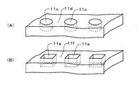
上記の実施の形態の構造体層11の凹部11aと凸部11bは溝と畝を交互に繰り返した周期的な構造の場合であるが、例えば図4のような構造でもよい。図4(A) は円形の縦穴形状の凹部11c、隣接する凹部11c,11cの間の部分を凸部11dとして構造体層11を構成したものである。また、図4 (B)は矩形の縦穴形状の凹部11e、隣接する凹部11e,11eの間の部分を凸部11fとして構造体層11を構成したものである。この場合も、一組の凹部11c及び凸部11dが1周期をなし、その1周期の長さDは、特定の赤外線の波長とされている。また、一組の凹部11e及び凸部11fが1周期をなし、その1周期の長さDは、特定の赤外線の波長とされている。
The
図5は実施の形態の二酸化炭素センサ100の要部を示す図であり、この二酸化炭素センサ100は、前記実施の形態の赤外線センサ10と、赤外線光源20と、ケース30とを有している。赤外線センサ10と赤外線光源20はケース30内に対向して配置されており、赤外線光源20からの赤外線IFが赤外線センサ10の構造体層11に向けて照射される。また、ケース30には、窓30a,30aが形成され、この窓30a,30aを介して雰囲気がケース30内に導入される。ここで、赤外線センサ10の構造体層11における前記凹部11a及び凸部11bの1周期の長さは二酸化炭素の吸収波長域の波長(例えば4.3μm)に設定されている。また、赤外線光源20は一定強度(一定スペクトル分布)の赤外線を含む光を照射するように構成されている。
FIG. 5 is a diagram illustrating a main part of the carbon dioxide sensor 100 according to the embodiment. The carbon dioxide sensor 100 includes the
以上の構成により、二酸化炭素センサ100の赤外線センサ10は、凹部11aと凸部11bの1周期の長さが二酸化炭素の吸収波長域(例えば、4.3μm)になっていることから、構造体層11は二酸化炭素に吸収される特定の波長の赤外線を選択的に吸収する。したがって、ケース30内の二酸化炭素濃度が高いと赤外線センサ10が検出する赤外線受光量は少なくなり、二酸化炭素濃度が低いと赤外線センサ10が検出する赤外線受光量は多くなる。また、赤外線光源20は一定強度の赤外線を照射しているので、この検出される赤外線受光量に基づいてケース30内の二酸化炭素濃度を検出することができる。
With the above configuration, the
なお、本発明の赤外線センサは、二酸化炭素検出センサのみならず、一酸化炭素センサや二酸化硫黄センサにも適用できる。一酸化炭素検出センサの場合には、凹部と凸部の1周期の長さを4.7μmとし、二酸化硫黄検出センサの場合には、凹部と凸部の1周期の長さを7.4μmとすればよい。 In addition, the infrared sensor of this invention is applicable not only to a carbon dioxide detection sensor but to a carbon monoxide sensor and a sulfur dioxide sensor. In the case of a carbon monoxide detection sensor, the length of one cycle of the concave portion and the convex portion is 4.7 μm, and in the case of the sulfur dioxide detection sensor, the length of one cycle of the concave portion and the convex portion is 7.4 μm. do it.
また、凹部と凸部の周期的構造を、周期の長さ(すなわち対応する特定の波長)が異なる複数の構造体層を形成すれば、特定の波長を有する複数種類の赤外線を検出することができる。 In addition, if a plurality of structural body layers having different period lengths (that is, corresponding specific wavelengths) are formed in the periodic structure of the concave and convex portions, a plurality of types of infrared rays having specific wavelengths can be detected. it can.
1 シリコン基板
11 構造体層
11a 凹部
11b 凸部
2 サーモパイル
21 平面部
10 赤外線センサ
20 赤外線光源
30 ケース
100 二酸化炭素センサ
DESCRIPTION OF
Claims (2)
当該赤外線センサの前記赤外線を受ける側に平面部を有する感温層と、該感温層の前記平面部側に形成された構造体層とを備え、
前記構造体層は、前記平面と平行な方向に凹凸が周期的に形成され、該凹凸の形状が該平面部と直角な面での断面形状が矩形波状で、かつ該凹凸の1周期の長さが前記特定の赤外線の波長と同程度としたことを特徴とする赤外線センサ。 An infrared sensor that detects infrared rays of a specific wavelength,
A temperature-sensitive layer having a plane portion on the side receiving the infrared rays of the infrared sensor, and a structure layer formed on the plane portion side of the temperature-sensitive layer,
In the structure layer, irregularities are periodically formed in a direction parallel to the plane, the irregular shape has a rectangular wave shape in a plane perpendicular to the plane portion, and the length of one period of the irregularities. The infrared sensor is characterized in that the length is approximately the same as the wavelength of the specific infrared ray.
前記赤外線センサの前記構造体層に対して赤外線を含む光を照射する赤外線光源と、
前記赤外線センサと前記赤外線光源との間に雰囲気が導入される空間を形成するケース体と、
を備えたことを特徴とする二酸化炭素センサ。 The infrared sensor according to claim 1, wherein the length of one cycle of the unevenness of the structure layer is an absorption wavelength region of carbon dioxide;
An infrared light source for irradiating the structure layer of the infrared sensor with light containing infrared;
A case body forming a space in which an atmosphere is introduced between the infrared sensor and the infrared light source;
A carbon dioxide sensor characterized by comprising:
Priority Applications (1)
| Application Number | Priority Date | Filing Date | Title |
|---|---|---|---|
| JP2008161881A JP5336114B2 (en) | 2008-06-20 | 2008-06-20 | Infrared sensor and carbon dioxide sensor |
Applications Claiming Priority (1)
| Application Number | Priority Date | Filing Date | Title |
|---|---|---|---|
| JP2008161881A JP5336114B2 (en) | 2008-06-20 | 2008-06-20 | Infrared sensor and carbon dioxide sensor |
Publications (2)
| Publication Number | Publication Date |
|---|---|
| JP2010002323A true JP2010002323A (en) | 2010-01-07 |
| JP5336114B2 JP5336114B2 (en) | 2013-11-06 |
Family
ID=41584170
Family Applications (1)
| Application Number | Title | Priority Date | Filing Date |
|---|---|---|---|
| JP2008161881A Expired - Fee Related JP5336114B2 (en) | 2008-06-20 | 2008-06-20 | Infrared sensor and carbon dioxide sensor |
Country Status (1)
| Country | Link |
|---|---|
| JP (1) | JP5336114B2 (en) |
Citations (9)
| Publication number | Priority date | Publication date | Assignee | Title |
|---|---|---|---|---|
| JPH01142418A (en) * | 1987-11-30 | 1989-06-05 | Toshiba Corp | Infrared-ray detecting element |
| JPH03216522A (en) * | 1990-01-22 | 1991-09-24 | Matsushita Electric Ind Co Ltd | Infrared detector for detection of flame |
| JPH06221919A (en) * | 1993-01-23 | 1994-08-12 | Horiba Ltd | Branching/condensing element for multielement pyroelectric detector |
| JPH09172227A (en) * | 1995-11-21 | 1997-06-30 | Thomson Csf | Photoelectron quantum well device |
| JP2005283435A (en) * | 2004-03-30 | 2005-10-13 | Japan Aviation Electronics Industry Ltd | Infrared sensor |
| JP2006047085A (en) * | 2004-08-04 | 2006-02-16 | Denso Corp | Infrared sensor device and its manufacturing method |
| JP2006524338A (en) * | 2003-04-22 | 2006-10-26 | レイセオン カンパニー | Integrated spectroscopic microbolometer with microfilter array |
| JP2006313164A (en) * | 2005-05-04 | 2006-11-16 | Tyco Electronics Raychem Gmbh | Gas sensor apparatus and gas measuring method |
| JP2007312012A (en) * | 2006-05-17 | 2007-11-29 | Toshiba Corp | Compact camera module |
-
2008
- 2008-06-20 JP JP2008161881A patent/JP5336114B2/en not_active Expired - Fee Related
Patent Citations (9)
| Publication number | Priority date | Publication date | Assignee | Title |
|---|---|---|---|---|
| JPH01142418A (en) * | 1987-11-30 | 1989-06-05 | Toshiba Corp | Infrared-ray detecting element |
| JPH03216522A (en) * | 1990-01-22 | 1991-09-24 | Matsushita Electric Ind Co Ltd | Infrared detector for detection of flame |
| JPH06221919A (en) * | 1993-01-23 | 1994-08-12 | Horiba Ltd | Branching/condensing element for multielement pyroelectric detector |
| JPH09172227A (en) * | 1995-11-21 | 1997-06-30 | Thomson Csf | Photoelectron quantum well device |
| JP2006524338A (en) * | 2003-04-22 | 2006-10-26 | レイセオン カンパニー | Integrated spectroscopic microbolometer with microfilter array |
| JP2005283435A (en) * | 2004-03-30 | 2005-10-13 | Japan Aviation Electronics Industry Ltd | Infrared sensor |
| JP2006047085A (en) * | 2004-08-04 | 2006-02-16 | Denso Corp | Infrared sensor device and its manufacturing method |
| JP2006313164A (en) * | 2005-05-04 | 2006-11-16 | Tyco Electronics Raychem Gmbh | Gas sensor apparatus and gas measuring method |
| JP2007312012A (en) * | 2006-05-17 | 2007-11-29 | Toshiba Corp | Compact camera module |
Also Published As
| Publication number | Publication date |
|---|---|
| JP5336114B2 (en) | 2013-11-06 |
Similar Documents
| Publication | Publication Date | Title |
|---|---|---|
| US7807061B2 (en) | Optical gas concentration detector and method of producing structure used in the detector | |
| CN105336809B (en) | Terahertz wave detector with arrays of conductive channel structure | |
| JP6257407B2 (en) | Infrared gas sensor | |
| JP6694503B2 (en) | Substrate for temperature measurement and temperature measurement system | |
| JP6538844B2 (en) | Sample Measurement Chip, Sample Measurement Device, and Sample Measurement Method | |
| JP2006220623A (en) | Fabry-perot interferometer and infrared sensor apparatus using same | |
| JP2009210312A (en) | Fabry-perot interferometer and method of manufacturing the same | |
| KR20180126584A (en) | Waveguide sensor with nanoporous surface layer | |
| US9612159B2 (en) | Infrared sensor and infrared sensor array | |
| JP2007201475A (en) | Narrow band transmission filter for euv radiation | |
| JP5336114B2 (en) | Infrared sensor and carbon dioxide sensor | |
| WO2016024503A1 (en) | Gas measurement apparatus, multiple-device substrate, manufacturing methods therefor, and methods for manufacturing infrared light source and pyroelectric infrared sensor | |
| JP2006275632A (en) | Spectroscopic gas sensor | |
| JP2010127892A (en) | Infrared sensor | |
| JP2019174354A (en) | Light receiving and emitting device and optical concentration measuring device | |
| JP5943882B2 (en) | Toner amount detection sensor | |
| US20190258038A1 (en) | Highly-folding pendular optical cavity | |
| US11921031B2 (en) | Compact gas sensor | |
| JP2010127891A (en) | Infrared sensor and method of manufacturing same | |
| JP2009150699A (en) | System for measuring position of object to be measured | |
| JP4207128B2 (en) | Infrared light source and infrared gas analyzer | |
| JP2009288057A (en) | Profile measuring apparatus | |
| US11592384B2 (en) | Device and method for detecting particles and method for manufacturing same | |
| JP2018054546A (en) | Radiation temperature measurement unit | |
| US10684214B2 (en) | Optical cavity with strong dynamic |
Legal Events
| Date | Code | Title | Description |
|---|---|---|---|
| A621 | Written request for application examination |
Free format text: JAPANESE INTERMEDIATE CODE: A621 Effective date: 20110428 |
|
| A977 | Report on retrieval |
Free format text: JAPANESE INTERMEDIATE CODE: A971007 Effective date: 20120524 |
|
| A131 | Notification of reasons for refusal |
Free format text: JAPANESE INTERMEDIATE CODE: A131 Effective date: 20120605 |
|
| A521 | Written amendment |
Free format text: JAPANESE INTERMEDIATE CODE: A523 Effective date: 20120806 |
|
| A131 | Notification of reasons for refusal |
Free format text: JAPANESE INTERMEDIATE CODE: A131 Effective date: 20130108 |
|
| A521 | Written amendment |
Free format text: JAPANESE INTERMEDIATE CODE: A523 Effective date: 20130311 |
|
| TRDD | Decision of grant or rejection written | ||
| A01 | Written decision to grant a patent or to grant a registration (utility model) |
Free format text: JAPANESE INTERMEDIATE CODE: A01 Effective date: 20130709 |
|
| A61 | First payment of annual fees (during grant procedure) |
Free format text: JAPANESE INTERMEDIATE CODE: A61 Effective date: 20130801 |
|
| R150 | Certificate of patent or registration of utility model |
Free format text: JAPANESE INTERMEDIATE CODE: R150 |
|
| LAPS | Cancellation because of no payment of annual fees |