JP2010000124A - Interface circuit and electrical stimulation measuring method - Google Patents
Interface circuit and electrical stimulation measuring method Download PDFInfo
- Publication number
- JP2010000124A JP2010000124A JP2008159168A JP2008159168A JP2010000124A JP 2010000124 A JP2010000124 A JP 2010000124A JP 2008159168 A JP2008159168 A JP 2008159168A JP 2008159168 A JP2008159168 A JP 2008159168A JP 2010000124 A JP2010000124 A JP 2010000124A
- Authority
- JP
- Japan
- Prior art keywords
- switch circuit
- electrical stimulation
- circuit
- amplifier
- microelectrode
- Prior art date
- Legal status (The legal status is an assumption and is not a legal conclusion. Google has not performed a legal analysis and makes no representation as to the accuracy of the status listed.)
- Granted
Links
Images


Landscapes
- Electrotherapy Devices (AREA)
- Measurement And Recording Of Electrical Phenomena And Electrical Characteristics Of The Living Body (AREA)
- User Interface Of Digital Computer (AREA)
Abstract
Description
本発明は、生体へのインタフェース回路及び電子刺激計測方法について、特に、生体組織や神経細胞等に対して電気刺激信号を印加するとともに、電気的刺激信号により励起される生体組織や神経細胞等の電気的活動を計測する際に有効な技術に関する。 The present invention relates to an interface circuit to a living body and an electronic stimulus measurement method, in particular, an electrical stimulus signal is applied to a living tissue, a nerve cell, etc. The present invention relates to a technique effective in measuring electrical activity.
従来、生体や脳の情報伝達メカニズムの解明を目的として、多点電極を用いて生体や神経細胞由来の電気信号(以下「生体電気信号」という)を計測することが広く行われている。また、近年は生体や脳との情報交信の実現を目指して、多点電極を介して外部から生体や神経細胞に対して情報を入力することを目的とするいわゆるブレイン・マシンインタフェースの技術について様々な研究が行われている。 2. Description of the Related Art Conventionally, for the purpose of elucidating the information transmission mechanism of a living body or a brain, it is widely performed to measure an electrical signal derived from a living body or a nerve cell (hereinafter referred to as “bioelectric signal”) using a multipoint electrode. In recent years, with the aim of realizing information communication with the living body and the brain, various technologies of so-called brain-machine interface, which aims to input information to the living body and nerve cells from the outside via multipoint electrodes, have been developed. Research has been conducted.
このような生体電気信号のインタフェースとして、例えば特許文献1には、生体や神経細胞とのインタフェースとなる多点電極と、多点電極で計測された微弱な生体電気信号を増幅するための増幅部と、増幅された生体電気信号を記録するための記録部と、生体への電気刺激信号を印加するための電気刺激信号印加部とから構成されるシステムが示されている。ここでは、同一の微小電極を介して、生体への電気刺激信号の送信と、生体から生体電気信号を検出して記録することとの双方を行うことができ、さらに電気刺激信号の送信の完了後、回路のスイッチを切替えることによってごく短時間で生体電気信号の検出を開始し、記録することを可能とするシステムが提案されている。 As such a bioelectric signal interface, for example, Patent Document 1 discloses a multipoint electrode serving as an interface with a living body or a nerve cell, and an amplifying unit for amplifying a weak bioelectric signal measured by the multipoint electrode. And a system comprising a recording unit for recording the amplified bioelectric signal and an electrical stimulation signal application unit for applying an electrical stimulation signal to the living body. Here, both the transmission of the electrical stimulation signal to the living body and the detection and recording of the biological electrical signal from the living body can be performed through the same microelectrode, and the transmission of the electrical stimulation signal is completed. Later, a system has been proposed that enables detection and recording of bioelectric signals in a very short time by switching the circuit switch.
また、近年、このような生体電気信号記録装置の生体への装着や設置を実現するために、システムのICチップ化による小型化、省電力化の検討が進められている。例えば非特許文献1には、CMOSプロセスを用いることにより、生体由来の電気信号の記録と生体への電気刺激信号の印加を1つのICチップで行う技術が示されている。
しかしながら、特許文献1の技術では、入力増幅器で増幅された生体電気信号を直流電位保持回路に保持し、スイッチが切り替わった場合に、直流電位保持回路に保持された電圧がそのまま電気刺激信号に加算されるため、スイッチの切替えと電気刺激信号の印加に伴う生体からの過渡応答が大きくなるという問題があった。また、電気信号発生装置と主増幅器とインタフェース回路とを制御するパーソナルコンピュータからの制御信号は、複数の微小電極のそれぞれに同時に送信されるため、複数の微小電極のうち任意の微小電極に対して、他の微小電極と異なるタイミングで電気信号を印加することはできない。さらに、特許文献1に記載されたインタフェース回路は、アナログスイッチ回路やサンプルホールド回路などの個別部品を組み合わせて構成したものであり、インタフェース回路が大きいため、生体への設置や装着は困難であった。 However, in the technique of Patent Document 1, when the bioelectric signal amplified by the input amplifier is held in the DC potential holding circuit and the switch is switched, the voltage held in the DC potential holding circuit is added to the electrical stimulation signal as it is. Therefore, there has been a problem that a transient response from a living body accompanying switching of a switch and application of an electrical stimulation signal becomes large. In addition, since the control signal from the personal computer that controls the electric signal generator, the main amplifier, and the interface circuit is simultaneously transmitted to each of the plurality of microelectrodes, any one of the plurality of microelectrodes can be controlled. An electric signal cannot be applied at a timing different from that of other microelectrodes. Furthermore, the interface circuit described in Patent Document 1 is configured by combining individual components such as an analog switch circuit and a sample-and-hold circuit. Since the interface circuit is large, it is difficult to install and attach to a living body. .
本発明は、このような状況に鑑みてなされたもので、生体への電気刺激信号の印加前後の微小電極の電位変動を小さくし、また、複数の微小電極のそれぞれに応じた制御により電気刺激信号を印加しそれに伴う生体電気信号を検出することを可能とする電気刺激信号制御回路および電気刺激信号制御方法を提供することを目的とする。 The present invention has been made in view of such a situation, and it is possible to reduce the potential fluctuation of the microelectrode before and after the application of the electrical stimulation signal to the living body, and to perform electrical stimulation by control according to each of the plurality of microelectrodes. An object of the present invention is to provide an electrical stimulation signal control circuit and an electrical stimulation signal control method capable of detecting a bioelectric signal accompanying the application of a signal.
上述した課題を解決するために、本発明は、微小電極と、微小電極に接続されるインタフェース回路と、インタフェース回路を介して微小電極に電気刺激信号を印加する電気刺激信号発生装置と、インタフェース回路を介して微小電極からの生体電気信号を増幅する主増幅器と、を備えた電気刺激計測装置におけるインタフェース回路であって、微小電極からの生体電気信号を定められた増幅率で増幅する入力増幅器と、入力増幅器から主増幅器に入力される生体電気信号の直流電位を保持する直流電位保持回路と、直流電位保持回路からの直流電位を、入力増幅器の増幅率の略逆数の増幅率で増幅する保持電位増幅器と、電気刺激信号発生装置からの電気刺激信号と保持電位増幅器からの直流電位とを加算する加算器と、入力増幅器と直流電位保持回路との間に接続される第1のスイッチ回路と、保持電位増幅器と主増幅器との間に接続される第2のスイッチ回路と、加算回路と電気刺激信号発生装置との間に接続される第3のスイッチ回路と、微小電極と加算回路との間に接続される第4のスイッチ回路とを備えることを特徴とする。 In order to solve the above-described problems, the present invention provides a microelectrode, an interface circuit connected to the microelectrode, an electrical stimulation signal generator for applying an electrical stimulation signal to the microelectrode via the interface circuit, and an interface circuit A main amplifier that amplifies the bioelectric signal from the microelectrode via an interface circuit in an electrical stimulation measurement device comprising: an input amplifier that amplifies the bioelectric signal from the microelectrode at a predetermined amplification rate; A DC potential holding circuit that holds the DC potential of the bioelectric signal input from the input amplifier to the main amplifier, and a holding that amplifies the DC potential from the DC potential holding circuit at an amplification factor that is approximately the inverse of the amplification factor of the input amplifier. A potential amplifier, an adder for adding the electrical stimulation signal from the electrical stimulation signal generator and the direct current potential from the holding potential amplifier, an input amplifier and a direct current A first switch circuit connected between the potential holding circuit, a second switch circuit connected between the holding potential amplifier and the main amplifier, and a connection between the adding circuit and the electrical stimulation signal generator. And a fourth switch circuit connected between the microelectrode and the addition circuit.
また、本発明は、上述のインタフェース回路は、CMOSプロセスを用いて作成されたトリプルウェル構造により構成されることを特徴とする。 The present invention is characterized in that the above-described interface circuit has a triple well structure formed by using a CMOS process.
また、本発明は、上述のインタフェース回路は、接続された制御手段からの制御により、通常時は第3のスイッチ回路および第4のスイッチ回路をオフにするとともに第1のスイッチ回路および第2のスイッチ回路をオンにして微小電極に主増幅器が接続された状態とし、電気刺激を実行する場合には、第3のスイッチ回路をオンにするとともに第1のスイッチ回路および第2のスイッチ回路をオフにして微小電極から主増幅器を切り離した後、第4のスイッチ回路をオンにして電気刺激信号を印加し、電気刺激終了後一定時間、第4のスイッチ回路および第3のスイッチ回路がオンで第1のスイッチ回路および第2のスイッチ回路がオフの状態を保ち、その後通常時の状態に戻す制御が行われることを特徴とする。 Further, according to the present invention, the interface circuit described above turns off the third switch circuit and the fourth switch circuit in a normal state and controls the first switch circuit and the second switch circuit under the control of the connected control means. When the switch circuit is turned on and the main amplifier is connected to the microelectrode and electrical stimulation is performed, the third switch circuit is turned on and the first switch circuit and the second switch circuit are turned off. After disconnecting the main amplifier from the microelectrode, the fourth switch circuit is turned on to apply the electrical stimulation signal, and the fourth switch circuit and the third switch circuit are turned on for a certain time after the electrical stimulation is finished. Control is performed such that the first switch circuit and the second switch circuit are kept off and then returned to the normal state.
また、本発明は、微小電極と、微小電極に接続されるインタフェースモジュールと、インタフェースモジュールを介して微小電極に電気刺激信号を印加する電気刺激信号発生装置と、インタフェースモジュールを介して微小電極からの生体電気信号を増幅する主増幅器と、の組み合わせを複数組備えた電気刺激計測装置において複数のインタフェースモジュールを備えるインタフェース回路であって、インタフェースモジュールは、微小電極からの生体電気信号を定められた増幅率で増幅する入力増幅器と、入力増幅器から主増幅器に入力される生体電気信号の直流電位を保持する直流電位保持回路と、直流電位保持回路からの直流電位を、入力増幅器の増幅率の略逆数の増幅率で増幅する保持電位増幅器と、電気刺激信号発生装置からの電気刺激信号と保持電位増幅器からの直流電位とを加算する加算器と、入力増幅器と直流電位保持回路との間に接続される第1のスイッチ回路と、保持電位増幅器と主増幅器との間に接続される第2のスイッチ回路と、加算回路と電気刺激信号発生装置との間に接続される第3のスイッチ回路と、微小電極と加算回路との間に接続される第4のスイッチ回路とを備えることを特徴とする。 The present invention also provides a microelectrode, an interface module connected to the microelectrode, an electrical stimulation signal generator for applying an electrical stimulation signal to the microelectrode via the interface module, and a microelectrode via the interface module. An interface circuit including a plurality of interface modules in an electrical stimulation measuring apparatus including a plurality of combinations of a main amplifier for amplifying bioelectric signals, wherein the interface module is configured to amplify bioelectric signals from microelectrodes. An input amplifier that amplifies at a rate, a DC potential holding circuit that holds the DC potential of a bioelectric signal input from the input amplifier to the main amplifier, and a DC potential from the DC potential holding circuit that is substantially the inverse of the amplification factor of the input amplifier A holding potential amplifier that amplifies at an amplification factor of An adder for adding the stimulation signal and the DC potential from the holding potential amplifier, a first switch circuit connected between the input amplifier and the DC potential holding circuit, and a connection between the holding potential amplifier and the main amplifier A second switch circuit, a third switch circuit connected between the addition circuit and the electrical stimulation signal generator, and a fourth switch circuit connected between the microelectrode and the addition circuit. It is characterized by providing.
また、本発明は、上述のインタフェースモジュールは、CMOSプロセスを用いて作成されたトリプルウェル構造により構成されることを特徴とする。 The present invention is characterized in that the above-mentioned interface module is constituted by a triple well structure formed by using a CMOS process.
また、本発明は、上述のインタフェースモジュールは、接続された制御手段からの制御により、組み合わせのそれぞれについて、通常時は第3のスイッチ回路および第4のスイッチ回路をオフにするとともに第1のスイッチ回路および第2のスイッチ回路をオンにして微小電極に主増幅器が接続された状態とし、電気刺激を実行する場合には、第3のスイッチ回路をオンにするとともに第1のスイッチ回路および第2のスイッチ回路をオフにして微小電極から主増幅器を切り離した後、第4のスイッチ回路をオンにして電気刺激信号を印加し、電気刺激終了後一定時間、第4のスイッチ回路および第3のスイッチ回路がオンで第1のスイッチ回路および第2のスイッチ回路がオフの状態を保ち、その後通常時の状態に戻す制御が行われることを特徴とする。 Further, according to the present invention, the interface module described above turns off the third switch circuit and the fourth switch circuit in the normal state and controls the first switch for each combination under the control of the connected control means. In a case where the main amplifier is connected to the microelectrode by turning on the circuit and the second switch circuit, and the electrical stimulation is executed, the third switch circuit is turned on and the first switch circuit and the second switch circuit are turned on. The switch circuit is turned off to disconnect the main amplifier from the microelectrode, and then the fourth switch circuit is turned on to apply the electrical stimulation signal. After the electrical stimulation is finished, the fourth switch circuit and the third switch Control is performed to keep the first switch circuit and the second switch circuit off while the circuit is on and then return to the normal state. And features.
また、本発明は、微小電極と、微小電極に接続されるインタフェース回路と、インタフェース回路を介して微小電極に電気刺激信号を印加する電気刺激信号発生装置と、インタフェース回路を介して微小電極からの生体電気信号を増幅する主増幅器と、インタフェース回路、電気刺激信号発生装置、及び主増幅器を制御する制御手段と、を具備する電気刺激計測装置を用いた電気刺激計測方法であって、インタフェース回路は、微小電極からの生体電気信号を定められた増幅率で増幅する入力増幅器と、入力増幅器から主増幅器に入力される生体電気信号の直流電位を保持する直流電位保持回路と、直流電位保持回路からの直流電位を、入力増幅器の増幅率の略逆数の増幅率で増幅する保持電位増幅器と、電気刺激信号発生装置からの電気刺激信号と保持電位増幅器からの直流電位とを加算する加算器と、入力増幅器と直流電位保持回路との間に接続される第1のスイッチ回路と、保持電位増幅器と主増幅器との間に接続される第2のスイッチ回路と、加算回路と電気刺激信号発生装置との間に接続される第3のスイッチ回路と、微小電極と加算回路との間に接続される第4のスイッチ回路とを備えるものであり、制御手段が、通常時は第3のスイッチ回路および第4のスイッチ回路をオフにするとともに第1のスイッチ回路および第2のスイッチ回路をオンにして微小電極に主増幅器が接続された状態とし、電気刺激を実行する場合には、第3のスイッチ回路をオンにするとともに第1のスイッチ回路および第2のスイッチ回路をオフにして微小電極から主増幅器を切り離した後、第4のスイッチ回路をオンにして電気刺激信号を印加し、電気刺激終了後一定時間、第4のスイッチ回路および第3のスイッチ回路がオンで第1のスイッチ回路および第2のスイッチ回路がオフの状態を保ち、その後通常時の状態に戻す制御を行うことを特徴とする。 The present invention also provides a microelectrode, an interface circuit connected to the microelectrode, an electrical stimulation signal generator for applying an electrical stimulation signal to the microelectrode via the interface circuit, and a microelectrode via the interface circuit. An electrical stimulation measurement method using an electrical stimulation measurement apparatus comprising: a main amplifier that amplifies a biological electrical signal; an interface circuit; an electrical stimulation signal generator; and a control unit that controls the main amplifier. An input amplifier that amplifies the bioelectric signal from the microelectrode with a predetermined amplification factor, a DC potential holding circuit that holds the DC potential of the bioelectric signal input from the input amplifier to the main amplifier, and a DC potential holding circuit A holding potential amplifier that amplifies the DC potential of the input amplifier with an amplification factor that is approximately the inverse of the amplification factor of the input amplifier, An adder for adding the signal and the DC potential from the holding potential amplifier, a first switch circuit connected between the input amplifier and the DC potential holding circuit, and connected between the holding potential amplifier and the main amplifier. A second switch circuit, a third switch circuit connected between the adder circuit and the electrical stimulation signal generator, and a fourth switch circuit connected between the microelectrode and the adder circuit. The control means normally turns off the third switch circuit and the fourth switch circuit and turns on the first switch circuit and the second switch circuit to connect the main amplifier to the microelectrode. When the electrical stimulation is performed, the third switch circuit is turned on and the first switch circuit and the second switch circuit are turned off to disconnect the main amplifier from the microelectrode. The fourth switch circuit is turned on to apply the electrical stimulation signal, and the fourth switch circuit and the third switch circuit are turned on and the first switch circuit and the second switch circuit are turned off for a certain time after the electrical stimulation is finished. It is characterized in that control is performed to maintain this state and then return to the normal state.
また、本発明は、微小電極と、微小電極に接続されるインタフェースモジュールと、インタフェースモジュールを介して微小電極に電気刺激信号を印加する電気刺激信号発生装置と、インタフェースモジュールを介して微小電極からの生体電気信号を増幅する主増幅器と、インタフェースモジュール、電気刺激信号発生装置、及び主増幅器の複数組の組み合わせのそれぞれを制御する制御手段と、を備える電気刺激計測装置を用いた電気刺激計測方法であって、インタフェースモジュールは、微小電極からの生体電気信号を定められた増幅率で増幅する入力増幅器と、入力増幅器から主増幅器に入力される生体電気信号の直流電位を保持する直流電位保持回路と、直流電位保持回路からの直流電位を、入力増幅器の増幅率の略逆数の増幅率で増幅する保持電位増幅器と、電気刺激信号発生装置からの電気刺激信号と保持電位増幅器からの直流電位とを加算する加算器と、入力増幅器と直流電位保持回路との間に接続される第1のスイッチ回路と、保持電位増幅器と主増幅器との間に接続される第2のスイッチ回路と、加算回路と電気刺激信号発生装置との間に接続される第3のスイッチ回路と、微小電極と加算回路との間に接続される第4のスイッチ回路とを備えるものであり、制御手段は、組み合わせのそれぞれについて、通常時は第3のスイッチ回路および第4のスイッチ回路をオフにするとともに第1のスイッチ回路および第2のスイッチ回路をオンにして微小電極に主増幅器が接続された状態とし、電気刺激を実行する場合には、第3のスイッチ回路をオンにするとともに第1のスイッチ回路および第2のスイッチ回路をオフにして微小電極から主増幅器を切り離した後、第4のスイッチ回路をオンにして電気刺激信号を印加し、電気刺激終了後一定時間、第4のスイッチ回路および第3のスイッチ回路がオンで第1のスイッチ回路および第2のスイッチ回路がオフの状態を保ち、その後通常時の状態に戻す制御を行うことを特徴とする。 The present invention also provides a microelectrode, an interface module connected to the microelectrode, an electrical stimulation signal generator for applying an electrical stimulation signal to the microelectrode via the interface module, and a microelectrode via the interface module. An electrical stimulation measurement method using an electrical stimulation measurement apparatus comprising: a main amplifier that amplifies a biological electrical signal; and an interface module, an electrical stimulation signal generation device, and a control unit that controls each of a plurality of combinations of the main amplifier. The interface module includes an input amplifier that amplifies the bioelectric signal from the microelectrode with a predetermined amplification factor, and a DC potential holding circuit that holds the DC potential of the bioelectric signal input from the input amplifier to the main amplifier. , The DC potential from the DC potential holding circuit with an amplification factor that is approximately the reciprocal of the amplification factor of the input amplifier. A holding potential amplifier that widens, an adder that adds the electrical stimulation signal from the electrical stimulation signal generator and the DC potential from the holding potential amplifier, and a first amplifier connected between the input amplifier and the DC potential holding circuit. A switch circuit; a second switch circuit connected between the holding potential amplifier and the main amplifier; a third switch circuit connected between the adder circuit and the electrical stimulation signal generator; And a fourth switch circuit connected to the circuit, and the control means normally turns off the third switch circuit and the fourth switch circuit for each of the combinations and turns off the first switch circuit. In the case where the main amplifier is connected to the microelectrode by turning on the switch circuit and the second switch circuit and performing electrical stimulation, the third switch circuit is turned on. The first switch circuit and the second switch circuit are turned off to disconnect the main amplifier from the microelectrode, and then the fourth switch circuit is turned on to apply the electrical stimulation signal. Control is performed such that the switch circuit and the third switch circuit are turned on, the first switch circuit and the second switch circuit are kept off, and then returned to the normal state.
以上説明したように、本発明によれば、微小電極に接続されるインタフェース回路と、インタフェース回路を介して微小電極に電気刺激信号を印加する電気刺激信号発生装置と、インタフェース回路を介して微小電極からの生体電気信号を増幅する主増幅器とを、制御手段によるスイッチの制御によって、通常時には、微小電極と入力増幅器と主増幅器とが接続され、加算回路と電気刺激信号発生装置とが切り離された状態とし、その後、微小電極と入力増幅器と主増幅器とを切り離すと同時に電気刺激信号発生装置と加算回路とを接続し、直流電位保持回路に保持された電位を、入力増幅器の増幅率の略逆数となる増幅率の保持電位増幅器によって増幅し、電気刺激信号発生装置からの電気刺激信号に加算して、微小電極に印加するようにしたので、入力増幅器によって増幅されて保持された電位を、保持電位増幅器によって増幅前の電位としてから電気刺激信号に加算することができ、生体への電気刺激信号の印加前後の微小電極の電位変動を小さくすることが可能となる。 As described above, according to the present invention, the interface circuit connected to the microelectrode, the electrical stimulation signal generator for applying the electrical stimulation signal to the microelectrode via the interface circuit, and the microelectrode via the interface circuit The main amplifier that amplifies the bioelectric signal from the device is normally connected to the microelectrode, the input amplifier, and the main amplifier by the control of the switch by the control means, and the addition circuit and the electrical stimulation signal generator are disconnected. After that, the microelectrode, the input amplifier, and the main amplifier are disconnected, and at the same time, the electrical stimulation signal generator and the adding circuit are connected, and the potential held in the DC potential holding circuit is approximately the inverse of the amplification factor of the input amplifier. It is amplified by the holding potential amplifier of the amplification factor to be added to the electrical stimulation signal from the electrical stimulation signal generator and applied to the microelectrode Therefore, the potential amplified and held by the input amplifier can be added to the electrical stimulation signal after being converted to the potential before amplification by the holding potential amplifier, and the potential fluctuation of the microelectrode before and after application of the electrical stimulation signal to the living body Can be reduced.
また、本発明によれば、インタフェース回路は、CMOSプロセスを用いて作成されたトリプルウェル構造により構成されるようにしたので、インタフェース回路を、生体への設置や装着が可能な大きさとすることが可能となる。 Further, according to the present invention, the interface circuit is configured by a triple well structure created by using a CMOS process, so that the interface circuit can be sized to be installed and mounted on a living body. It becomes possible.
また、本発明によれば、微小電極に接続されるインタフェース回路と、インタフェース回路を介して微小電極に電気刺激信号を印加する電気刺激信号発生装置と、インタフェース回路を介して微小電極からの生体電気信号を増幅する主増幅器とを制御する制御手段との組み合わせを複数組備え、制御手段により動作を制御するようにしたので、複数の微小電極のそれぞれについて、異なる制御を行うことが可能となる。 Further, according to the present invention, an interface circuit connected to the microelectrode, an electrical stimulation signal generator for applying an electrical stimulation signal to the microelectrode via the interface circuit, and bioelectricity from the microelectrode via the interface circuit Since a plurality of combinations with the control means for controlling the main amplifier for amplifying the signal are provided and the operation is controlled by the control means, different control can be performed for each of the plurality of microelectrodes.
以下、本発明の一実施形態について、図面を参照して説明する。
<第1の実施形態>
図1は、本発明の第1の実施形態によるインタフェース回路2を用いた生体電気信号記録システムの構成を示すブロック図である。
本実施形態による生体電気信号記録システムは、微小電極1と、インタフェース回路2と、電気刺激信号発生装置3と、主増幅器4と、制御手段であるパーソナルコンピュータ5とを備えている。
Hereinafter, an embodiment of the present invention will be described with reference to the drawings.
<First Embodiment>
FIG. 1 is a block diagram showing a configuration of a bioelectric signal recording system using an
The bioelectric signal recording system according to the present embodiment includes a microelectrode 1, an
微小電極1は、生体の細胞等に設置された電極である。
インタフェース回路2は、微小電極1と、電気刺激信号発生装置3と、主増幅器4と、パーソナルコンピュータ5とに接続される。インタフェース回路2は、パーソナルコンピュータ5から送信される制御信号に基づいて、電気刺激信号発生装置3から入力される電気信号を、微小電極1を介して生体に印加し、一方、微小電極1から検出される生体由来の生体電気信号を、主増幅器4に出力する。また、インタフェース回路2は、トリプルウェル構造を有するCMOS技術によって構成される。
The microelectrode 1 is an electrode installed on a living body cell or the like.
The
電気刺激信号発生装置3は、パーソナルコンピュータ5から送信される制御信号に応じて、電気刺激信号を出力する。
主増幅器4は、パーソナルコンピュータ5から送信される制御信号に応じて、インタフェース回路2を介して入力される生体電気信号を増幅し、パーソナルコンピュータ5に出力する。主増幅器4で増幅された生体電気信号は、アナログ・デジタル変換されて、パーソナルコンピュータ5の記録手段(例えば、ハードディスク)等に記録される。
パーソナルコンピュータ5は、インタフェース回路2と、電気刺激信号発生装置3と、主増幅器4とのそれぞれに制御信号を送信して動作を制御する。また、微小電極1から検出され、インタフェース回路2を介して主増幅器4で増幅された生体電気信号を記録する。
The electrical
The
The
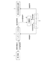
図2は、図1に示すインタフェース回路2の具体的な構成を示すブロック図である。
インタフェース回路2は、加算回路21と、入力増幅器22と、直流電位保持回路23と、スイッチ回路241と、スイッチ回路242と、スイッチ回路243と、スイッチ回路244とを備えている。
FIG. 2 is a block diagram showing a specific configuration of the
The
ここで、スイッチ回路243の一端は、電気刺激信号発生装置3に接続され、他端は、加算回路21の加算器211の入力端の一端に接続される。また、スイッチ回路242の一端は、主増幅器4に接続されており、他端は、加算回路21の保持電位増幅器212の入力端に接続される。保持電位増幅器212の出力端は、加算器211の入力端の他端に接続される。加算器211の出力端は、スイッチ回路244の一端に接続され、スイッチ回路244の他端は、微小電極1と、入力増幅器22の入力端の一端に接続される。入力増幅器22の入力端の他端は、接地される。入力増幅器22の出力端は、スイッチ回路241の一端に接続される。スイッチ回路241の他端は、分岐され、直流電位保持回路23の一端およびスイッチ回路242の一端に接続される。直流電位保持回路23の他端は、接地される。
Here, one end of the
入力増幅器22は、微小電極1から出力される生体電気信号を増幅する。ここで、入力増幅器22の増幅率をαとする。
加算回路21は、加算器211と保持電位増幅器212とを備えている。保持電位増幅器212は、直流電位保持回路23の出力電圧を、入力増幅器22の増幅率の略逆数の増幅率で増幅する。ここでは、1/αとなる。
直流電位保持回路23には、入力増幅器22から出力される生体信号の直流電位が保持される。
The
The
The DC
第1のスイッチ回路であるスイッチ回路241は、入力増幅器22と直流電位保持回路23との間に接続される。
第2のスイッチ回路であるスイッチ回路242は、保持電位増幅器212と主増幅器4との間に接続される。
第3のスイッチ回路であるスイッチ回路243は、加算器211と電気刺激信号発生装置3との間に接続される。
第4のスイッチ回路であるスイッチ回路244は、微小電極1と加算器211との間に接続される。
The
The
A
A
ここで、スイッチ回路241、スイッチ回路242、スイッチ回路243、スイッチ回路244は、パーソナルコンピュータ5からの制御信号により、図3に示すタイミングで制御される。通常時、生体からの生体電気信号記録時(時刻<t1、またはt4<時刻)は、スイッチ回路241およびスイッチ回路242がオン、スイッチ回路243およびスイッチ回路244がオフになっている。このとき、微小電極1と入力増幅器22と主増幅器4とが接続され、加算回路21と電気刺激信号発生装置3とは切り離されている。
Here, the
微小電極1に電気刺激信号を印加するときは、まず時刻t1においてスイッチ回路241およびスイッチ回路242がオフに、スイッチ回路243がオンになる。スイッチ回路244はオフのままである。このとき、主増幅器4の入力電位は、直流電位保持回路23により、切り離す直前の入力増幅器22の出力電位に保持される。直流電位保持回路23から加算器211への出力は、増幅器212を介して1/α倍されるため、切り離す直前の微小電極の電位となる。
When an electrical stimulation signal is applied to the microelectrode 1, first, at time t1, the
さらに、時刻t2においてスイッチ回路244をオンにした後、時刻t3において電気刺激信号発生装置3から電気刺激信号が出力されて微小電極1に印加され、生体組織や細胞の電気的活動が励起される。時刻t3に電気刺激信号が出力された後、一定時間、スイッチ回路241およびスイッチ回路242はオフ、スイッチ回路243およびスイッチ回路244はオンの状態に保たれる。このとき、直流電位保持回路23の出力電位が保持電位増幅器212によって1/α倍した電位が、微小電極1に印加される。
Further, after the
次に、本実施形態による生体電気信号記録システムの動作例を説明する。通常時(時刻<t1時点)には、スイッチ回路241およびスイッチ回路242がオン、スイッチ回路243およびスイッチ回路244がオフになっており、微小電極1と入力増幅器22と主増幅器4とが接続され、加算回路21と電気刺激信号発生装置3とが切り離された状態となっている。こここでは、微小電極1から検出された生体電気信号が、入力増幅器22によって増幅されて、また主増幅器4によって増幅されてパーソナルコンピュータ5に入力される。パーソナルコンピュータ5は、入力される生体電気信号を記録する。
Next, an operation example of the bioelectric signal recording system according to the present embodiment will be described. At normal time (time <t1), the
その後、スイッチ回路241およびスイッチ回路242をオフに、スイッチ回路243をオンにすることで、微小電極1と入力増幅器22と主増幅器4とを切り離すと同時に、加算回路21と電気刺激信号発生装置3とを接続する。これにより、直流電位保持回路23に保持された電位が、入力増幅器22の増幅率の略逆数となる増幅率をもつ保持電位増幅器212によって増幅され、電気刺激信号発生装置3からの電気刺激信号に加算される。そして、スイッチ回路244をオンにした後、パーソナルコンピュータ5からの制御信号に応じて、電気刺激信号発生装置3が、電気刺激信号を出力する。ここで、直流電位保持回路23から出力される電位が、電気刺激信号発生装置3に加算され、微小電極に印加される。その後、スイッチ回路241およびスイッチ回路242がオン、スイッチ回路243およびスイッチ回路244がオフになり、生体電気信号の記録が再開される。
Thereafter, by turning off the
以上の動作により、電気刺激信号の印加前後における微小電極1の電位は、電気刺激信号を印加する直前の微小電極1の直流電位に保たれるため、微小電極1の電位変動は最小に抑え、微小電極の直流電位のオフセット補償を行うことが可能となる。また、これらをCMOSプロセスにより作成されたICチップで実現するため、インタフェース回路を、生体への設置や装着が可能な大きさとすることが可能となる。 With the above operation, the potential of the microelectrode 1 before and after the application of the electrical stimulation signal is maintained at the direct current potential of the microelectrode 1 immediately before the electrical stimulation signal is applied. It becomes possible to perform offset compensation of the DC potential of the microelectrode. In addition, since these are realized by an IC chip created by a CMOS process, the interface circuit can be sized so that it can be installed and mounted on a living body.
<第2の実施形態>
図4は、本発明の第2の実施形態のインタフェース回路2−2を用いた生体電気信号記録システムの構成を示すブロック図である。第2の実施形態の生体電気信号記録システムは、第1の実施形態と同様に構成されており、同様の構成、動作については説明を省略する。
<Second Embodiment>
FIG. 4 is a block diagram showing a configuration of a bioelectric signal recording system using the interface circuit 2-2 according to the second embodiment of the present invention. The bioelectric signal recording system of the second embodiment is configured in the same manner as in the first embodiment, and the description of the same configuration and operation is omitted.
インタフェース回路2−2は、加算器211aと増幅器212aとからなる加算回路21a、入力増幅器22a、直流電位保持回路23a、スイッチ回路241a、スイッチ回路242a、スイッチ回路243a、スイッチ回路244aを備え、これらの組み合わせをインタフェースモジュールとしてn個(nは任意の数)備えている。これらのインタフェースモジュールが、微小電極1a〜n、電気刺激信号発生装置3a〜n、主増幅器4a〜nのそれぞれに対応付けられて接続されており、インタフェース回路2−2、電気刺激信号発生装置3a〜n、主増幅器4a〜nは、パーソナルコンピュータ5−2から送信される制御信号によって動作が制御される。また、インタフェース回路2−2は、トリプルウェル構造を有するCMOS技術によって実現できる。それぞれの電気刺激信号発生装置3i、主増幅器4iと、スイッチ回路241i、スイッチ回路242i、スイッチ回路243i、スイッチ回路244i(i=a〜n)の開閉は、パーソナルコンピュータ5により独立または同期して制御される。
The interface circuit 2-2 includes an
このように、本実施形態によれば、複数の微小電極の中の一つ以上の任意の微小電極を選択して、生体祖織、あるいは細胞に対して順次電気刺激を与え、複数の電気刺激に対する複数の生体電気信号を微小電極で検出して記録することを、CMOSプロセスにより作成されたICチップで行うことが可能となる。 As described above, according to the present embodiment, one or more arbitrary microelectrodes among a plurality of microelectrodes are selected, and electrical stimulation is sequentially applied to a living tissue or a cell. It is possible to detect and record a plurality of bioelectric signals with respect to a microelectrode with an IC chip created by a CMOS process.
以上説明したように、本発明によれば、微小電極を介して生体への電気刺激信号の出力と生体電気信号の入力をする際に、電気刺激信号の印加による微小電極の電位の変動を抑えることが可能となる。また、本発明によれば、電気刺激と生体電気信号の記録をする際、生体へのインタフェース回路の設置が可能となり、微小電極とインタフェース回路との距離を短くして、ノイズの混入を抑えることが可能となる。さらに、本発明によれば、複数の微小電極の電位の変動を、電極毎に制御することが可能になる。 As described above, according to the present invention, when the electrical stimulation signal is output to the living body and the biological electrical signal is input through the microelectrode, the fluctuation of the potential of the microelectrode due to the application of the electrical stimulation signal is suppressed. It becomes possible. In addition, according to the present invention, when recording electrical stimulation and bioelectric signals, it is possible to install an interface circuit to the living body, and the distance between the microelectrode and the interface circuit is shortened to suppress noise contamination. Is possible. Furthermore, according to the present invention, it is possible to control the fluctuation of the potentials of a plurality of microelectrodes for each electrode.
1、1a〜n・・・・・・・・・・微小電極
2・・・・・・・・・・・・・・・インタフェース回路
21、21a〜n・・・・・・・・加算回路
211、211a〜n・・・・・・加算器
212、212a〜n・・・・・・保持電位増幅器
22、22a〜n・・・・・・・・入力増幅器
23、23a〜n・・・・・・・・直流電位保持回路
241、241a〜n、242、242a〜n、243、243a〜n、244、244a〜n・・・・・・・・・・・・スイッチ回路
3、3a〜n・・・・・・・・・・電気刺激信号発生回路
4、4a〜n・・・・・・・・・・主増幅器
1, 1a to n ...
Claims (8)
前記微小電極からの生体電気信号を定められた増幅率で増幅する入力増幅器と、
前記入力増幅器から前記主増幅器に入力される生体電気信号の直流電位を保持する直流電位保持回路と、
前記直流電位保持回路からの直流電位を、前記入力増幅器の前記増幅率の略逆数の増幅率で増幅する保持電位増幅器と、
前記電気刺激信号発生装置からの電気刺激信号と前記保持電位増幅器からの直流電位とを加算する加算器と、
前記入力増幅器と前記直流電位保持回路との間に接続される第1のスイッチ回路と、
前記保持電位増幅器と前記主増幅器との間に接続される第2のスイッチ回路と、
前記加算回路と前記電気刺激信号発生装置との間に接続される第3のスイッチ回路と、
前記微小電極と前記加算回路との間に接続される第4のスイッチ回路と
を備えることを特徴とするインタフェース回路。 A microelectrode, an interface circuit connected to the microelectrode, an electrical stimulation signal generator for applying an electrical stimulation signal to the microelectrode via the interface circuit, and a living body from the microelectrode via the interface circuit A main amplifier for amplifying an electrical signal, and the interface circuit in the electrical stimulation measuring device comprising:
An input amplifier that amplifies the bioelectric signal from the microelectrode at a predetermined amplification rate;
A DC potential holding circuit for holding a DC potential of a bioelectric signal input from the input amplifier to the main amplifier;
A holding potential amplifier that amplifies the DC potential from the DC potential holding circuit with an amplification factor that is approximately the inverse of the amplification factor of the input amplifier;
An adder for adding the electrical stimulation signal from the electrical stimulation signal generator and the DC potential from the holding potential amplifier;
A first switch circuit connected between the input amplifier and the DC potential holding circuit;
A second switch circuit connected between the holding potential amplifier and the main amplifier;
A third switch circuit connected between the adder circuit and the electrical stimulation signal generator;
An interface circuit comprising: a fourth switch circuit connected between the microelectrode and the adder circuit.
ことを特徴とする請求項1に記載のインタフェース回路。 The interface circuit according to claim 1, wherein the interface circuit includes a triple well structure created using a CMOS process.
ことを特徴とする請求項1または請求項2に記載のインタフェース回路。 The interface circuit normally turns off the third switch circuit and the fourth switch circuit and controls the first switch circuit and the second switch circuit under the control of the connected control means. When the main amplifier is connected to the microelectrode and the electrical stimulation is performed, the third switch circuit is turned on and the first switch circuit and the second switch circuit are turned on. Is turned off to disconnect the main amplifier from the microelectrode, and then the fourth switch circuit is turned on to apply an electrical stimulation signal, and after the electrical stimulation is finished, the fourth switch circuit and the third switch The first switch circuit and the second switch circuit are kept off while the switch circuit is turned on, and then control is performed to return to the normal state. Interface circuit according to claim 1 or claim 2, characterized in that.
前記インタフェースモジュールは、
前記微小電極からの生体電気信号を定められた増幅率で増幅する入力増幅器と、
前記入力増幅器から前記主増幅器に入力される生体電気信号の直流電位を保持する直流電位保持回路と、
前記直流電位保持回路からの直流電位を、前記入力増幅器の前記増幅率の略逆数の増幅率で増幅する保持電位増幅器と、
前記電気刺激信号発生装置からの電気刺激信号と前記保持電位増幅器からの直流電位とを加算する加算器と、
前記入力増幅器と前記直流電位保持回路との間に接続される第1のスイッチ回路と、
前記保持電位増幅器と前記主増幅器との間に接続される第2のスイッチ回路と、
前記加算回路と前記電気刺激信号発生装置との間に接続される第3のスイッチ回路と、
前記微小電極と前記加算回路との間に接続される第4のスイッチ回路と
を備えることを特徴とするインタフェース回路。 A microelectrode, an interface module connected to the microelectrode, an electrical stimulation signal generator for applying an electrical stimulation signal to the microelectrode via the interface module, and a living body from the microelectrode via the interface module The interface circuit including the plurality of interface modules in an electrical stimulation measuring apparatus including a plurality of combinations of a main amplifier that amplifies an electrical signal,
The interface module is
An input amplifier that amplifies the bioelectric signal from the microelectrode at a predetermined amplification rate;
A DC potential holding circuit for holding a DC potential of a bioelectric signal input from the input amplifier to the main amplifier;
A holding potential amplifier that amplifies the DC potential from the DC potential holding circuit with an amplification factor that is approximately the inverse of the amplification factor of the input amplifier;
An adder for adding the electrical stimulation signal from the electrical stimulation signal generator and the DC potential from the holding potential amplifier;
A first switch circuit connected between the input amplifier and the DC potential holding circuit;
A second switch circuit connected between the holding potential amplifier and the main amplifier;
A third switch circuit connected between the adder circuit and the electrical stimulation signal generator;
An interface circuit comprising: a fourth switch circuit connected between the microelectrode and the adder circuit.
ことを特徴とする請求項4に記載のインタフェース回路。 The interface circuit according to claim 4, wherein the interface module includes a triple well structure created using a CMOS process.
ことを特徴とする請求項4または請求項5に記載のインタフェース回路。 The interface module normally turns off the third switch circuit and the fourth switch circuit and controls the first switch circuit and the fourth switch circuit for each of the combinations under control from a connected control unit. When the second switch circuit is turned on so that the main amplifier is connected to the microelectrode and electrical stimulation is performed, the third switch circuit is turned on and the first switch circuit and After turning off the second switch circuit and disconnecting the main amplifier from the microelectrode, the fourth switch circuit is turned on and an electrical stimulation signal is applied. The switch circuit and the third switch circuit are on, and the first switch circuit and the second switch circuit are off Maintaining, interface circuit according to claim 4 or claim 5 then control for returning to the state at the normal time, characterized in that takes place.
前記微小電極に接続されるインタフェース回路と、
前記インタフェース回路を介して前記微小電極に電気刺激信号を印加する電気刺激信号発生装置と、
前記インタフェース回路を介して前記微小電極からの生体電気信号を増幅する主増幅器と、
前記インタフェース回路、前記電気刺激信号発生装置、及び前記主増幅器を制御する制御手段と、を具備する電気刺激計測装置を用いた電気刺激計測方法であって、
前記インタフェース回路は、
前記微小電極からの生体電気信号を定められた増幅率で増幅する入力増幅器と、
前記入力増幅器から前記主増幅器に入力される生体電気信号の直流電位を保持する直流電位保持回路と、
前記直流電位保持回路からの直流電位を、前記入力増幅器の前記増幅率の略逆数の増幅率で増幅する保持電位増幅器と、
前記電気刺激信号発生装置からの電気刺激信号と前記保持電位増幅器からの直流電位とを加算する加算器と、
前記入力増幅器と前記直流電位保持回路との間に接続される第1のスイッチ回路と、
前記保持電位増幅器と前記主増幅器との間に接続される第2のスイッチ回路と、
前記加算回路と前記電気刺激信号発生装置との間に接続される第3のスイッチ回路と、
前記微小電極と前記加算回路との間に接続される第4のスイッチ回路と
を備えるものであり、
前記制御手段が、通常時は前記第3のスイッチ回路および前記第4のスイッチ回路をオフにするとともに前記第1のスイッチ回路および前記第2のスイッチ回路をオンにして前記微小電極に前記主増幅器が接続された状態とし、電気刺激を実行する場合には、前記第3のスイッチ回路をオンにするとともに前記第1のスイッチ回路および前記第2のスイッチ回路をオフにして前記微小電極から前記主増幅器を切り離した後、前記第4のスイッチ回路をオンにして電気刺激信号を印加し、電気刺激終了後一定時間、前記第4のスイッチ回路および前記第3のスイッチ回路がオンで前記第1のスイッチ回路および前記第2のスイッチ回路がオフの状態を保ち、その後通常時の状態に戻す制御を行う
ことを特徴とする電気刺激計測方法。 Microelectrodes,
An interface circuit connected to the microelectrode;
An electrical stimulation signal generator for applying electrical stimulation signals to the microelectrodes via the interface circuit;
A main amplifier for amplifying a bioelectric signal from the microelectrode via the interface circuit;
An electrical stimulation measurement method using an electrical stimulation measurement device comprising the interface circuit, the electrical stimulation signal generation device, and a control means for controlling the main amplifier,
The interface circuit is
An input amplifier that amplifies the bioelectric signal from the microelectrode at a predetermined amplification rate;
A DC potential holding circuit for holding a DC potential of a bioelectric signal input from the input amplifier to the main amplifier;
A holding potential amplifier that amplifies the DC potential from the DC potential holding circuit with an amplification factor that is approximately the inverse of the amplification factor of the input amplifier;
An adder for adding the electrical stimulation signal from the electrical stimulation signal generator and the DC potential from the holding potential amplifier;
A first switch circuit connected between the input amplifier and the DC potential holding circuit;
A second switch circuit connected between the holding potential amplifier and the main amplifier;
A third switch circuit connected between the adder circuit and the electrical stimulation signal generator;
A fourth switch circuit connected between the microelectrode and the addition circuit,
The control means normally turns off the third switch circuit and the fourth switch circuit and turns on the first switch circuit and the second switch circuit to turn the main amplifier on the microelectrode. When the electrical stimulation is executed, the third switch circuit is turned on, the first switch circuit and the second switch circuit are turned off, and the main electrode is turned off from the microelectrode. After disconnecting the amplifier, the fourth switch circuit is turned on to apply the electrical stimulation signal. After the electrical stimulation is finished, the fourth switch circuit and the third switch circuit are turned on for a certain period of time. An electrical stimulation measurement method comprising: controlling the switch circuit and the second switch circuit to be in an off state and then returning to a normal state.
前記微小電極に接続されるインタフェースモジュールと、
前記インタフェースモジュールを介して前記微小電極に電気刺激信号を印加する電気刺激信号発生装置と、
前記インタフェースモジュールを介して前記微小電極からの生体電気信号を増幅する主増幅器と、
前記インタフェースモジュール、前記電気刺激信号発生装置、及び前記主増幅器の複数組の組み合わせのそれぞれを制御する制御手段と、を備える電気刺激計測装置を用いた電気刺激計測方法であって、
前記インタフェースモジュールは、
前記微小電極からの生体電気信号を定められた増幅率で増幅する入力増幅器と、
前記入力増幅器から前記主増幅器に入力される生体電気信号の直流電位を保持する直流電位保持回路と、
前記直流電位保持回路からの直流電位を、前記入力増幅器の前記増幅率の略逆数の増幅率で増幅する保持電位増幅器と、
前記電気刺激信号発生装置からの電気刺激信号と前記保持電位増幅器からの直流電位とを加算する加算器と、
前記入力増幅器と前記直流電位保持回路との間に接続される第1のスイッチ回路と、
前記保持電位増幅器と前記主増幅器との間に接続される第2のスイッチ回路と、
前記加算回路と前記電気刺激信号発生装置との間に接続される第3のスイッチ回路と、
前記微小電極と前記加算回路との間に接続される第4のスイッチ回路と
を備えるものであり、
前記制御手段は、前記組み合わせのそれぞれについて、通常時は前記第3のスイッチ回路および前記第4のスイッチ回路をオフにするとともに前記第1のスイッチ回路および前記第2のスイッチ回路をオンにして前記微小電極に前記主増幅器が接続された状態とし、電気刺激を実行する場合には、前記第3のスイッチ回路をオンにするとともに前記第1のスイッチ回路および前記第2のスイッチ回路をオフにして前記微小電極から前記主増幅器を切り離した後、前記第4のスイッチ回路をオンにして電気刺激信号を印加し、電気刺激終了後一定時間、前記第4のスイッチ回路および前記第3のスイッチ回路がオンで前記第1のスイッチ回路および前記第2のスイッチ回路がオフの状態を保ち、その後通常時の状態に戻す制御を行う
ことを特徴とする電気刺激計測方法。 Microelectrodes,
An interface module connected to the microelectrode;
An electrical stimulation signal generator for applying electrical stimulation signals to the microelectrodes via the interface module;
A main amplifier for amplifying a bioelectric signal from the microelectrode via the interface module;
A control means for controlling each of a plurality of combinations of the interface module, the electrical stimulation signal generator, and the main amplifier, and an electrical stimulation measurement method using an electrical stimulation measurement device comprising:
The interface module is
An input amplifier that amplifies the bioelectric signal from the microelectrode at a predetermined amplification rate;
A DC potential holding circuit for holding a DC potential of a bioelectric signal input from the input amplifier to the main amplifier;
A holding potential amplifier that amplifies the DC potential from the DC potential holding circuit with an amplification factor that is approximately the inverse of the amplification factor of the input amplifier;
An adder for adding the electrical stimulation signal from the electrical stimulation signal generator and the DC potential from the holding potential amplifier;
A first switch circuit connected between the input amplifier and the DC potential holding circuit;
A second switch circuit connected between the holding potential amplifier and the main amplifier;
A third switch circuit connected between the adder circuit and the electrical stimulation signal generator;
A fourth switch circuit connected between the microelectrode and the addition circuit,
The control means normally turns off the third switch circuit and the fourth switch circuit and turns on the first switch circuit and the second switch circuit for each of the combinations. When the main amplifier is connected to the microelectrode and electrical stimulation is performed, the third switch circuit is turned on and the first switch circuit and the second switch circuit are turned off. After disconnecting the main amplifier from the microelectrode, the fourth switch circuit is turned on to apply an electrical stimulation signal, and after the electrical stimulation is finished, the fourth switch circuit and the third switch circuit The first switch circuit and the second switch circuit are kept in an off state when turned on, and then controlled to return to a normal state. Electrical stimulation measurement method.
Priority Applications (1)
| Application Number | Priority Date | Filing Date | Title |
|---|---|---|---|
| JP2008159168A JP5008608B2 (en) | 2008-06-18 | 2008-06-18 | Interface circuit and electrical stimulation measurement method |
Applications Claiming Priority (1)
| Application Number | Priority Date | Filing Date | Title |
|---|---|---|---|
| JP2008159168A JP5008608B2 (en) | 2008-06-18 | 2008-06-18 | Interface circuit and electrical stimulation measurement method |
Publications (2)
| Publication Number | Publication Date |
|---|---|
| JP2010000124A true JP2010000124A (en) | 2010-01-07 |
| JP5008608B2 JP5008608B2 (en) | 2012-08-22 |
Family
ID=41582344
Family Applications (1)
| Application Number | Title | Priority Date | Filing Date |
|---|---|---|---|
| JP2008159168A Active JP5008608B2 (en) | 2008-06-18 | 2008-06-18 | Interface circuit and electrical stimulation measurement method |
Country Status (1)
| Country | Link |
|---|---|
| JP (1) | JP5008608B2 (en) |
Cited By (1)
| Publication number | Priority date | Publication date | Assignee | Title |
|---|---|---|---|---|
| CN110523000A (en) * | 2019-08-06 | 2019-12-03 | 深圳市理邦精密仪器股份有限公司 | A kind of EGC analog device |
Citations (6)
| Publication number | Priority date | Publication date | Assignee | Title |
|---|---|---|---|---|
| JPS5294683A (en) * | 1976-02-04 | 1977-08-09 | Daiya Med Syst | Small electrode device |
| JPS57125738A (en) * | 1981-01-28 | 1982-08-05 | Nippon Koden Kogyo Kk | Induction switch circuit in live body signal amplifier circuit |
| JPS62323A (en) * | 1985-06-07 | 1987-01-06 | 日本光電工業株式会社 | Addition averaging method of living body inducing signal |
| JPH02140142A (en) * | 1988-11-18 | 1990-05-29 | Sharp Corp | Electrocardiograph |
| JP2000041658A (en) * | 1998-07-30 | 2000-02-15 | Nippon Telegr & Teleph Corp <Ntt> | Bioelectric signal recorder, bioelectric signal recording, and electric stimulation |
| JP2008520153A (en) * | 2004-11-15 | 2008-06-12 | コーニンクレッカ フィリップス エレクトロニクス エヌ ヴィ | Adiabatic CMOS design |
-
2008
- 2008-06-18 JP JP2008159168A patent/JP5008608B2/en active Active
Patent Citations (6)
| Publication number | Priority date | Publication date | Assignee | Title |
|---|---|---|---|---|
| JPS5294683A (en) * | 1976-02-04 | 1977-08-09 | Daiya Med Syst | Small electrode device |
| JPS57125738A (en) * | 1981-01-28 | 1982-08-05 | Nippon Koden Kogyo Kk | Induction switch circuit in live body signal amplifier circuit |
| JPS62323A (en) * | 1985-06-07 | 1987-01-06 | 日本光電工業株式会社 | Addition averaging method of living body inducing signal |
| JPH02140142A (en) * | 1988-11-18 | 1990-05-29 | Sharp Corp | Electrocardiograph |
| JP2000041658A (en) * | 1998-07-30 | 2000-02-15 | Nippon Telegr & Teleph Corp <Ntt> | Bioelectric signal recorder, bioelectric signal recording, and electric stimulation |
| JP2008520153A (en) * | 2004-11-15 | 2008-06-12 | コーニンクレッカ フィリップス エレクトロニクス エヌ ヴィ | Adiabatic CMOS design |
Cited By (2)
| Publication number | Priority date | Publication date | Assignee | Title |
|---|---|---|---|---|
| CN110523000A (en) * | 2019-08-06 | 2019-12-03 | 深圳市理邦精密仪器股份有限公司 | A kind of EGC analog device |
| CN110523000B (en) * | 2019-08-06 | 2023-07-28 | 深圳市理邦精密仪器股份有限公司 | Electrocardiogram simulation device |
Also Published As
| Publication number | Publication date |
|---|---|
| JP5008608B2 (en) | 2012-08-22 |
Similar Documents
| Publication | Publication Date | Title |
|---|---|---|
| EP3111835B1 (en) | Sensing device with array of microelectrodes | |
| Lopez et al. | 22.7 A 966-electrode neural probe with 384 configurable channels in 0.13 µm SOI CMOS | |
| US8914099B2 (en) | Biomedical acquisition system with motion artifact reduction | |
| KR101937676B1 (en) | Bio signal amplifying circuit | |
| TW200703853A (en) | POL system architecture with analog bus | |
| Raducanu et al. | Time multiplexed active neural probe with 678 parallel recording sites | |
| JP2012508611A5 (en) | ||
| JP6713482B2 (en) | Active electrode, sensor system, and potential difference detection method | |
| MX2009008834A (en) | System and method for operating an electrochemical analyte sensor. | |
| CN102647156B (en) | Low-distortion dynamic current boost amplifier and associated method | |
| WO2008008777A3 (en) | Amplifier employing interleaved signals for pwm ripple suppression | |
| KR20170107479A (en) | Amplifying circuit | |
| Mulberry et al. | Analysis of simple half-shared transimpedance amplifier for picoampere biosensor measurements | |
| JP2012157695A (en) | Receiving circuit, ultrasonic probe, and ultrasonic image displaying apparatus | |
| US20190052251A1 (en) | Apparatus and method for signal processing by converting amplified difference signal | |
| JP5008608B2 (en) | Interface circuit and electrical stimulation measurement method | |
| JP2006317369A (en) | Open/short test device | |
| Xu et al. | A 60nV/v Hz 15-Channel Digital Active Electrode System for Portable Biopotential Signal Acquisition | |
| TWI257107B (en) | Low power dissipating sense amplifier | |
| EP2645621A1 (en) | Network apparatus | |
| Angotzi et al. | A high temporal resolution multiscale recording system for in vivo neural studies | |
| JP3566860B2 (en) | Bioelectric signal recording device, bioelectric signal recording method, and electrical stimulation method | |
| JP6919651B2 (en) | Semiconductor device and cell potential measuring device | |
| KR20180090090A (en) | Power supplying apparatus for neural activity recorder reducing common-mode signal applied in electordes connected to the neural activity recorder | |
| JP4928402B2 (en) | Electrical activity stimulus measurement method and electrical activity stimulus measurement device |
Legal Events
| Date | Code | Title | Description |
|---|---|---|---|
| RD04 | Notification of resignation of power of attorney |
Free format text: JAPANESE INTERMEDIATE CODE: A7424 Effective date: 20100526 |
|
| A621 | Written request for application examination |
Free format text: JAPANESE INTERMEDIATE CODE: A621 Effective date: 20100908 |
|
| A977 | Report on retrieval |
Free format text: JAPANESE INTERMEDIATE CODE: A971007 Effective date: 20120517 |
|
| TRDD | Decision of grant or rejection written | ||
| A01 | Written decision to grant a patent or to grant a registration (utility model) |
Free format text: JAPANESE INTERMEDIATE CODE: A01 Effective date: 20120522 |
|
| A01 | Written decision to grant a patent or to grant a registration (utility model) |
Free format text: JAPANESE INTERMEDIATE CODE: A01 |
|
| A61 | First payment of annual fees (during grant procedure) |
Free format text: JAPANESE INTERMEDIATE CODE: A61 Effective date: 20120529 |
|
| R150 | Certificate of patent or registration of utility model |
Ref document number: 5008608 Country of ref document: JP Free format text: JAPANESE INTERMEDIATE CODE: R150 Free format text: JAPANESE INTERMEDIATE CODE: R150 |
|
| FPAY | Renewal fee payment (event date is renewal date of database) |
Free format text: PAYMENT UNTIL: 20150608 Year of fee payment: 3 |
|
| S531 | Written request for registration of change of domicile |
Free format text: JAPANESE INTERMEDIATE CODE: R313531 |
|
| R350 | Written notification of registration of transfer |
Free format text: JAPANESE INTERMEDIATE CODE: R350 |
|
| R250 | Receipt of annual fees |
Free format text: JAPANESE INTERMEDIATE CODE: R250 |
|
| S111 | Request for change of ownership or part of ownership |
Free format text: JAPANESE INTERMEDIATE CODE: R313117 |
|
| R350 | Written notification of registration of transfer |
Free format text: JAPANESE INTERMEDIATE CODE: R350 |