JP2009540506A - Method for manufacturing confinement layer and device manufactured using the same - Google Patents
Method for manufacturing confinement layer and device manufactured using the same Download PDFInfo
- Publication number
- JP2009540506A JP2009540506A JP2009514349A JP2009514349A JP2009540506A JP 2009540506 A JP2009540506 A JP 2009540506A JP 2009514349 A JP2009514349 A JP 2009514349A JP 2009514349 A JP2009514349 A JP 2009514349A JP 2009540506 A JP2009540506 A JP 2009540506A
- Authority
- JP
- Japan
- Prior art keywords
- layer
- intermediate layer
- fluorinated
- forming
- surface energy
- Prior art date
- Legal status (The legal status is an assumption and is not a legal conclusion. Google has not performed a legal analysis and makes no representation as to the accuracy of the status listed.)
- Pending
Links
Images

Classifications
-
- H—ELECTRICITY
- H10—SEMICONDUCTOR DEVICES; ELECTRIC SOLID-STATE DEVICES NOT OTHERWISE PROVIDED FOR
- H10K—ORGANIC ELECTRIC SOLID-STATE DEVICES
- H10K71/00—Manufacture or treatment specially adapted for the organic devices covered by this subclass
- H10K71/10—Deposition of organic active material
- H10K71/12—Deposition of organic active material using liquid deposition, e.g. spin coating
- H10K71/13—Deposition of organic active material using liquid deposition, e.g. spin coating using printing techniques, e.g. ink-jet printing or screen printing
-
- H—ELECTRICITY
- H10—SEMICONDUCTOR DEVICES; ELECTRIC SOLID-STATE DEVICES NOT OTHERWISE PROVIDED FOR
- H10K—ORGANIC ELECTRIC SOLID-STATE DEVICES
- H10K71/00—Manufacture or treatment specially adapted for the organic devices covered by this subclass
-
- H—ELECTRICITY
- H10—SEMICONDUCTOR DEVICES; ELECTRIC SOLID-STATE DEVICES NOT OTHERWISE PROVIDED FOR
- H10K—ORGANIC ELECTRIC SOLID-STATE DEVICES
- H10K59/00—Integrated devices, or assemblies of multiple devices, comprising at least one organic light-emitting element covered by group H10K50/00
- H10K59/10—OLED displays
- H10K59/12—Active-matrix OLED [AMOLED] displays
-
- H—ELECTRICITY
- H10—SEMICONDUCTOR DEVICES; ELECTRIC SOLID-STATE DEVICES NOT OTHERWISE PROVIDED FOR
- H10K—ORGANIC ELECTRIC SOLID-STATE DEVICES
- H10K59/00—Integrated devices, or assemblies of multiple devices, comprising at least one organic light-emitting element covered by group H10K50/00
- H10K59/10—OLED displays
- H10K59/17—Passive-matrix OLED displays
Abstract
閉じ込められた第2の層を第1の層上に形成する方法であって:第1の表面エネルギーを有する第1の層を形成するステップと;第1の層上に、第1の層に直接接触する中間層を形成するステップであって、上記中間層が、第1の表面エネルギーよりも低い第2の表面エネルギーを有するステップと;中間層の選択された部分を除去して、第1の層の非被覆領域と第1の層の被覆領域とを含むパターンを形成するステップと;閉じ込められた第2の層を第1の層の非被覆領域上に形成するステップとを含む方法を提供する。この方法により製造された有機電子デバイスも提供する。 A method of forming a confined second layer on a first layer comprising: forming a first layer having a first surface energy; on the first layer, on the first layer Forming an intermediate layer in direct contact, wherein the intermediate layer has a second surface energy lower than the first surface energy; and removing a selected portion of the intermediate layer to form a first Forming a pattern including an uncovered area of the first layer and a covered area of the first layer; and forming a confined second layer on the uncovered area of the first layer. provide. An organic electronic device manufactured by this method is also provided.
Description
本開示は、一般に電子デバイスの製造方法に関する。本発明は、さらにその方法によって製造されたデバイスに関する。 The present disclosure relates generally to methods for manufacturing electronic devices. The invention further relates to a device manufactured by the method.
多くの種類の電子装置中には、有機活性材料を利用する電子デバイスが存在する。このようなデバイスにおいては、2つの電極の間に有機活性層が挟まれている。 In many types of electronic devices, there are electronic devices that utilize organic active materials. In such a device, an organic active layer is sandwiched between two electrodes.
電子デバイスの種類の1つに有機発光ダイオード(OLED)がある。OLEDは高電力変換効率および低加工費であるためにディスプレイ用途として有望である。このようなディスプレイは、携帯電話、携帯情報端末、携帯型パーソナルコンピュータ、およびDVDプレイヤなどの電池式携帯型電子デバイス用に特に有望である。これらの用途では、低電力消費以外に高情報量、フルカラー、および速いビデオ速度応答時間がディスプレイに要求される。 One type of electronic device is an organic light emitting diode (OLED). OLEDs are promising for display applications due to their high power conversion efficiency and low processing costs. Such displays are particularly promising for battery-powered portable electronic devices such as mobile phones, personal digital assistants, portable personal computers, and DVD players. In these applications, displays require high information content, full color, and fast video speed response time in addition to low power consumption.
フルカラーOLEDの製造における現在の研究は、費用対効果が大きく高生産性であるカラーピクセル製造方法の開発に向けられている。液処理によるモノクロディスプレイの製造の場合、スピンコーティング法が広く採用されている(たとえば、(非特許文献1)を参照されたい)。しかし、フルカラーディスプレイの製造では、モノクロディスプレイの製造に使用される方法に対してある変更を行う必要がある。たとえば、フルカラー画像を表示するために、各表示ピクセルを3つのサブピクセルに分解され、そのそれぞれがディスプレイの三原色の赤、緑、および青の1つを発する。このようなフルカラーピクセルの3つのサブピクセルへの分割の結果、液体着色材料(すなわちインク)の拡散および色の混合を防止するために現行方法を修正する必要が生じた。 Current research in the production of full-color OLEDs is directed to the development of cost-effective and high-productivity color pixel manufacturing methods. In the case of manufacturing a monochrome display by liquid processing, a spin coating method is widely adopted (for example, see (Non-patent Document 1)). However, in the production of full-color displays, certain changes need to be made to the methods used for the production of monochrome displays. For example, to display a full color image, each display pixel is broken down into three subpixels, each emitting one of the display's three primary colors red, green, and blue. As a result of this division of full-color pixels into three sub-pixels, there has been a need to modify current methods to prevent liquid coloring material (ie, ink) diffusion and color mixing.
インクを閉じ込めるためのいくつかの方法が文献に記載されている。これらは閉じ込め構造、表面張力の不連続性、およびこれら両方の組み合わせに基づいている。閉じ込め構造は、ピクセルのウェル、バンクなどの拡散の幾何学的な障害物である。効果的にするためには、これらの構造が、堆積される材料の湿潤厚さと同等の大きさとなる必要がある。これらの構造内に発光インクが印刷される場合、そのインクが構造表面をぬらし、そのためその構造付近で厚さの均一性が低下する。したがって、発光「ピクセル」領域の外側に移動させる必要があり、それによって動作中に不均一性が見えなくなる。ディスプレイ(特に高解像度ディスプレイ)上の空間は限られているため、これによってピクセルの利用可能な発光領域が減少する。実際の閉じ込め構造は、一般に、電荷注入層および電荷輸送層の連続層を堆積する場合の品質に悪影響を与える。この結果、すべての層を印刷する必要がある。 Several methods for confining ink are described in the literature. They are based on confinement structures, surface tension discontinuities, and a combination of both. The confinement structures are diffusional geometric obstacles such as pixel wells, banks. In order to be effective, these structures need to be as large as the wet thickness of the deposited material. When luminescent ink is printed in these structures, the ink wets the surface of the structure, thus reducing the thickness uniformity near the structure. Therefore, it must be moved outside the light emitting “pixel” region, thereby making the non-uniformity invisible during operation. This reduces the available light emitting area of the pixel, as the space on the display (especially the high resolution display) is limited. The actual confinement structure generally adversely affects the quality when depositing a continuous layer of charge injection layer and charge transport layer. As a result, all layers need to be printed.
さらに、低表面張力材料の印刷または気相堆積のいずれかが行われた領域が存在する場合には、表面張力の不連続性が生じる。これらの低表面張力材料は、一般に、ピクセル領域内に第1の有機活性層を印刷またはコーティングする前に適用する必要がある。一般に、これらの処理を使用すると、連続的な非発光層をコーティングする場合に品質に影響が生じるので、すべての層を印刷する必要がある。 Furthermore, surface tension discontinuities occur when there are areas where either low surface tension material printing or vapor deposition is present. These low surface tension materials generally need to be applied before printing or coating the first organic active layer in the pixel area. In general, the use of these processes has an impact on quality when coating continuous non-emissive layers, so all layers need to be printed.
2つのインク閉じ込め技術の併用の一例が、フォトレジストのバンク構造(ピクセルのウェル、チャネル)のCF4−プラズマ処理である。一般に、ピクセル領域内のすべての活性層を印刷する必要がある。 An example of the combined use of two ink confinement techniques is CF 4 -plasma treatment of photoresist bank structures (pixel wells, channels). In general, all active layers in the pixel area need to be printed.
これらすべての閉じ込め方法は、連続コーティングの妨害となる欠点を有する。より多い生産量およびより低い設備費用を得ることができるので、1つまたは複数の層の連続コーティングが望まれる。したがって、電子デバイスの改善された形成方法が必要とされている。 All these containment methods have the disadvantage of interfering with continuous coating. One or more layers of continuous coating are desired because higher production and lower equipment costs can be obtained. Accordingly, there is a need for improved methods of forming electronic devices.
閉じ込められた第2の層を第1の層上に形成する方法であって:
第1の表面エネルギーを有する第1の層を形成するステップと;
第1の層上に、第1の層に直接接触する中間層を形成するステップであって、前記中間層が、第1の表面エネルギーよりも低い第2の表面エネルギーを有するステップと;
中間層の選択された部分を除去して、第1の層の非被覆領域と第1の層の被覆領域とを含むパターンを形成するステップと;
閉じ込められた第2の層を第1の層の非被覆領域上に形成するステップとを含む方法を提供する。
A method of forming a confined second layer on a first layer comprising:
Forming a first layer having a first surface energy;
Forming an intermediate layer on the first layer in direct contact with the first layer, the intermediate layer having a second surface energy lower than the first surface energy;
Removing selected portions of the intermediate layer to form a pattern including uncovered areas of the first layer and covered areas of the first layer;
Forming a confined second layer on an uncovered region of the first layer.
電極上に配置された第1の有機活性層と第2の有機活性層とを含む有機電子デバイスの製造方法であって:
第1の表面エネルギーを有する第1の層を電極上に形成するステップと;
第1の層上に、第1の層に直接接触する中間層を形成するステップであって、前記中間層が、第1の表面エネルギーよりも低い第2の表面エネルギーを有するステップと;
中間層の選択された部分を除去して、第1の層の非被覆領域と第1の層の被覆領域とを含むパターンを形成するステップと;
閉じ込められた第2の層を第1の層の非被覆領域上に形成するステップとを含む方法を提供する。
A method of manufacturing an organic electronic device comprising a first organic active layer and a second organic active layer disposed on an electrode comprising:
Forming a first layer having a first surface energy on the electrode;
Forming an intermediate layer on the first layer in direct contact with the first layer, the intermediate layer having a second surface energy lower than the first surface energy;
Removing selected portions of the intermediate layer to form a pattern including uncovered areas of the first layer and covered areas of the first layer;
Forming a confined second layer on an uncovered region of the first layer.
電極上に配置された第1の有機活性層と第2の有機活性層とを含む有機電子デバイスであって、第1の有機活性層と第2の有機活性層との間にパターン化された中間層をさらに含む有機電子デバイスも提供する。 An organic electronic device comprising a first organic active layer and a second organic active layer disposed on an electrode, wherein the organic electronic device is patterned between the first organic active layer and the second organic active layer An organic electronic device further comprising an intermediate layer is also provided.
以上の概要および以下の詳細な説明は、単に例示的および説明的なものであり、添付の特許請求の範囲によって規定される本発明を限定するものではない。 The foregoing summary and the following detailed description are exemplary and explanatory only and are not restrictive of the invention, which is defined by the appended claims.
本明細書において提示される概念の理解をすすめるために、添付の図面において実施形態を説明する。 In order to facilitate understanding of the concepts presented herein, embodiments are described in the accompanying drawings.
当業者であれば理解しているように、図面中の物体は、平易かつ明快にするために示されており、必ずしも縮尺通りに描かれているわけではない。たとえば、実施形態を理解しやすいようにするために、図面中の一部の物体の寸法が他の物体よりも誇張されている場合がある。 As will be appreciated by those skilled in the art, the objects in the drawings are shown for simplicity and clarity and are not necessarily drawn to scale. For example, in order to facilitate understanding of the embodiments, the dimensions of some objects in the drawings may be exaggerated more than other objects.
閉じ込められた第2の層を第1の層上に形成する方法であって:
第1の表面エネルギーを有する第1の層を形成するステップと;
第1の層上に、第1の層に直接接触する中間層を形成するステップであって、前記中間層が、第1の表面エネルギーよりも低い第2の表面エネルギーを有するステップと;
中間層の選択された部分を除去して、第1の層の非被覆領域と第1の層の被覆領域とを含むパターンを形成するステップと;
閉じ込められた第2の層を第1の層の非被覆領域上に形成するステップとを含む方法を提供する。
A method of forming a confined second layer on a first layer comprising:
Forming a first layer having a first surface energy;
Forming an intermediate layer on the first layer in direct contact with the first layer, the intermediate layer having a second surface energy lower than the first surface energy;
Removing selected portions of the intermediate layer to form a pattern including uncovered areas of the first layer and covered areas of the first layer;
Forming a confined second layer on an uncovered region of the first layer.
多数の態様および実施形態を以上に説明してきたが、これらは単に例示的で非限定的なものである。本明細書を読めば、本発明の範囲から逸脱しない他の態様および実施形態が実現可能であることが、当業者には分かるであろう。 Many aspects and embodiments have been described above and are merely exemplary and not limiting. After reading this specification, skilled artisans will appreciate that other aspects and embodiments are possible without departing from the scope of the invention.
いずれか1つまたは複数の本発明の実施形態のその他の特徴および利点は、以下の詳細な説明および特許請求の範囲から明らかとなるであろう。この詳細な説明では、最初に、用語の定義および説明を扱い、続いて、材料、方法、有機電子デバイス、ならびに最後に実施例を扱う。 Other features and advantages of any one or more embodiments of the invention will be apparent from the following detailed description and from the claims. This detailed description first deals with definitions and explanations of terms, followed by materials, methods, organic electronic devices, and finally examples.
(1.用語の定義および説明)
以下に説明する実施形態の詳細を扱う前に、一部の用語について定義または説明を行う。
(1. Definition and explanation of terms)
Before addressing details of the embodiments described below, some terms are defined or explained.
層または材料について言及される場合の用語「活性」は、電子的または電気放射的(electro−radiative)性質を示す層または材料を意味することを意図している。電子デバイス中、活性材料は、デバイスの動作を電子的に促進する。活性材料の例としては、電子または正孔のいずれであってもよい電荷を伝導、注入、輸送、または遮断する材料、ならびに、放射線を受けた場合に、放射線を放出したり電子−正孔対の濃度変化を示したりする材料が挙げられるが、これらに限定されるものではない。不活性材料の例としては、平坦化材料、絶縁材料、および環境障壁材料が挙げられるが、これらに限定されるものではない。 The term “active” when referring to a layer or material is intended to mean a layer or material that exhibits electronic or electro-radiative properties. In electronic devices, the active material electronically facilitates device operation. Examples of active materials include materials that conduct, inject, transport, or block charge, which can be either electrons or holes, and emit radiation or electron-hole pairs when receiving radiation. However, the present invention is not limited to these materials. Examples of inert materials include, but are not limited to, planarization materials, insulating materials, and environmental barrier materials.
層について言及される場合の用語「閉じ込められた」は、その層が堆積される領域を大きく越えて層が広がらないことを意味することを意図している。この層は、表面エネルギーの作用、または表面エネルギーの作用と物理的障壁構造との組み合わせによって閉じ込めることができる。 The term “confined” when referring to a layer is intended to mean that the layer does not spread well beyond the area where the layer is deposited. This layer can be confined by the action of surface energy or a combination of the action of surface energy and a physical barrier structure.
用語「電極」は、電子部品内のキャリアを移送するように構成された部材または構造を意味することを意図している。たとえば、電極は、アノード、カソード、コンデンサ電極、ゲート電極などであってよい。電極は、トランジスタ、コンデンサ、抵抗器、インダクタ、ダイオード、電子部品、電源、またはそれらのあらゆる組み合わせの一部を含むことができる。 The term “electrode” is intended to mean a member or structure configured to transport a carrier within an electronic component. For example, the electrode may be an anode, a cathode, a capacitor electrode, a gate electrode, and the like. The electrode can include a portion of a transistor, capacitor, resistor, inductor, diode, electronic component, power source, or any combination thereof.
用語「有機電子デバイス」は、1つまたは複数の有機半導体の層または材料を含むデバイスを意味することを意図している。有機電子デバイスとしては:(1)電気エネルギーを放射線に変換するデバイス(たとえば、発光ダイオード、発光ダイオードディスプレイ、ダイオードレーザー、または照明パネル)、(2)電子的過程を介して信号を検出するデバイス(たとえば、光検出器、光導電セル、フォトレジスタ、光スイッチ、光トランジスタ、光電管、赤外線(「IR」)検出器、またはバイオセンサー)、(3)放射線を電気エネルギーに変換するデバイス(たとえば、光起電力デバイスまたは太陽電池)、ならびに(4)1つまたは複数の有機半導体層を含む1つまたは複数の電子部品(たとえば、トランジスタまたはダイオード)を含むデバイス、ならびに項目(1)〜(4)のあらゆる組み合わせが挙げられるが、これらに限定されるものではない。 The term “organic electronic device” is intended to mean a device comprising one or more organic semiconductor layers or materials. Organic electronic devices include: (1) devices that convert electrical energy into radiation (eg, light emitting diodes, light emitting diode displays, diode lasers, or lighting panels), (2) devices that detect signals via electronic processes ( (E.g., a photodetector, photoconductive cell, photoresistor, optical switch, phototransistor, phototube, infrared ("IR") detector, or biosensor), (3) a device that converts radiation into electrical energy (e.g., light Electromotive force devices or solar cells), and (4) devices comprising one or more electronic components (eg, transistors or diodes) comprising one or more organic semiconductor layers, and items (1)-(4) Any combination is possible, but not limited to these.
有機化合物に言及される場合の用語「フッ素化」は、化合物中の1つまたは複数の水素原子がフッ素で置き換えられていることを意味することを意図している。この用語は、部分フッ素化材料および完全フッ素化材料を含んでいる。 The term “fluorinated” when referring to an organic compound is intended to mean that one or more hydrogen atoms in the compound have been replaced by fluorine. The term includes partially fluorinated materials and fully fluorinated materials.
用語「表面エネルギー」は、材料から単位面積の表面を形成するために必要なエネルギーである。表面エネルギーの特徴の1つは、ある表面エネルギーを有する液体材料が、それより低い表面エネルギーを有する表面をぬらさないということである。 The term “surface energy” is the energy required to form a unit area surface from a material. One characteristic of surface energy is that a liquid material having a certain surface energy does not wet a surface having a lower surface energy.
用語「層」は、用語「フィルム」と交換可能に使用され、希望する領域を覆うコーティングを意味する。この用語は大きさによって限定されない。この領域は、デバイス全体の大きさであってもよいし、実際の視覚的表示などの特殊な機能の領域の小ささ、または1つのサブピクセルの小ささであってもよい。層およびフィルムは、気相堆積、液相堆積(連続的技術および不連続技術)、および熱転写などの従来のあらゆる堆積技術によって形成することができる。 The term “layer” is used interchangeably with the term “film” and refers to a coating covering a desired area. This term is not limited by size. This area may be the size of the entire device, the area of a special function such as an actual visual display, or the size of one subpixel. Layers and films can be formed by any conventional deposition technique such as vapor deposition, liquid deposition (continuous and discontinuous techniques), and thermal transfer.
用語「液体組成物」は、材料が溶解して溶液を形成する液体媒体、材料が分散して分散液を形成する液体媒体、あるいは材料が懸濁して懸濁液またはエマルジョンを形成する液体媒体を意味することを意図している。「液体媒体」は、溶媒または担体流体を加えなくても液体である材料、すなわちその凝固温度よりも高い温度における材料を意味することを意図している。 The term “liquid composition” refers to a liquid medium in which the material dissolves to form a solution, a liquid medium in which the material is dispersed to form a dispersion, or a liquid medium in which the material is suspended to form a suspension or emulsion. Intended to mean. “Liquid medium” is intended to mean a material that is liquid without the addition of a solvent or carrier fluid, ie, a material at a temperature above its solidification temperature.
用語「液体閉じ込め構造」は、工作物の内部または上の構造であって、そのような1つまたは複数の構造が、それ自体または集合的に、工作物上を液体が流れる時にある領域内または範囲内に液体を束縛または案内する主機能を果たす構造を意味することを意図している。液体閉じ込め構造としては、カソードセパレーターまたはウェル構造を挙げることができる。 The term “liquid confinement structure” refers to a structure within or on a workpiece, in which one or more structures, either by themselves or collectively, are in an area when liquid flows over the workpiece or It is intended to mean a structure that performs the primary function of constraining or guiding a liquid within range. The liquid confinement structure can include a cathode separator or a well structure.
用語「液体媒体」は、純液体、複数の液体の組み合わせ、溶液、分散液、懸濁液、およびエマルジョンなどの液体材料を意味することを意図している。液体媒体は、1種類の溶媒が存在するか、複数の溶媒が存在するかとは無関係に使用される。 The term “liquid medium” is intended to mean liquid materials such as pure liquids, combinations of liquids, solutions, dispersions, suspensions, and emulsions. The liquid medium is used regardless of whether one or more solvents are present.
本明細書において使用される場合、用語「〜の上」は、ある層、部材、または構造が、別の層、部材、または構造のすぐ隣にあったり接触していたりすることを必ずしも意味しない。介在する層、部材、または構造がさらに存在する場合がある。 As used herein, the term “above” does not necessarily mean that one layer, member, or structure is next to or in contact with another layer, member, or structure. . There may be additional intervening layers, members, or structures.
本明細書において使用される場合、用語「含んでなる」、「含んでなること」、「含む」、「含むこと」、「有する」、「有すること」、またはそれらの他のあらゆる変形は、非排他的な包含を扱うことを意図している。たとえば、ある一連の要素を含むプロセス、方法、物品、または装置は、それらの要素にのみに必ずしも限定されるわけではなく、そのようなプロセス、方法、物品、または装置に関して明示されず固有のものでもない他の要素を含むことができる。さらに、反対の意味で明記されない限り、「または」は、包含的なまたはを意味するのであって、排他的なまたはを意味するのではない。たとえば、条件AまたはBが満たされるのは、Aが真であり(または存在し)Bが偽である(または存在しない)、Aが偽であり(または存在せず)Bが真である(または存在する)、ならびにAおよびBの両方が真である(または存在する)のいずれか1つによってである。 As used herein, the terms “comprising”, “comprising”, “comprising”, “comprising”, “having”, “having”, or any other variation thereof, Intended to deal with non-exclusive inclusions. For example, a process, method, article, or apparatus that includes a set of elements is not necessarily limited to only those elements, and is not explicitly or inherently related to such a process, method, article, or apparatus. But other elements can be included. Further, unless stated to the contrary, “or” means inclusive, not exclusive, or. For example, the condition A or B is satisfied when A is true (or exists), B is false (or does not exist), A is false (or does not exist) and B is true ( Or both) and both A and B are true (or present).
また、本発明の要素および成分を説明するために「a」または「an」も使用されている。これは単に便宜的なものであり、本発明の一般的な意味を提供するために行われている。この記述は、1つまたは少なくとも1つを含むものと読むべきであり、明らかに他の意味となる場合を除けば、単数形は複数形も含んでいる。 “A” or “an” is also used to describe elements and components of the present invention. This is merely for convenience and is done to provide a general sense of the invention. This description should be read to include one or at least one and the singular also includes the plural unless it is obvious that it is meant otherwise.
元素周期表中の縦列に対応する族の番号は、(非特許文献2)に見ることができる「新表記法」(New Notation)の規則を使用している。 The number of the group corresponding to the column in the periodic table of elements uses the rule of “New Notation” (Non-Patent Document 2) that can be seen in (Non-Patent Document 2).
特に定義しない限り、本明細書において使用されるすべての技術用語および科学用語は、本発明が属する技術分野の当業者によって一般に理解されている意味と同じ意味を有する。本明細書に記載されているものと類似または同等の方法および材料を使用して、本発明の実施形態の実施または試験を行うことができるが、好適な方法および材料については以下に説明する。本明細書において言及されるあらゆる刊行物、特許出願、特許、およびその他の参考文献は、特に明記しない限り、それらの記載内容全体が援用される。矛盾が生じる場合には、定義を含めて本明細書に従うものとする。さらに、材料、方法、および実施例は、単に説明的なものであって、限定を意図したものではない。 Unless defined otherwise, all technical and scientific terms used herein have the same meaning as commonly understood by one of ordinary skill in the art to which this invention belongs. Although methods and materials similar or equivalent to those described herein can be used to practice or test embodiments of the present invention, suitable methods and materials are described below. All publications, patent applications, patents, and other references mentioned herein are incorporated by reference in their entirety unless otherwise specified. In case of conflict, the present specification, including definitions, will control. In addition, the materials, methods, and examples are illustrative only and not intended to be limiting.
本明細書に記載されていない程度の、具体的な材料、処理行為、および回路に関する多くの詳細は従来通りであり、それらについては、有機発光ダイオードディスプレイ、光源、光検出器、光電池、および半導体要素の技術分野の教科書およびその他の情報源中に見ることができる。 Many details regarding specific materials, processing actions, and circuits to the extent not described herein are conventional, including organic light emitting diode displays, light sources, photodetectors, photovoltaic cells, and semiconductors. Can be found in textbooks and other sources of information on the technical field of the element
(2.材料)
第1および第2の層の材料は、それらが含まれる物品の意図する最終用途によって大部分は決定される。中間層の材料は、第2の層が閉じ込められるように選択される。これは、中間層の表面エネルギーが第1の層の表面エネルギー未満となるように調整することで行われる。
(2. Materials)
The materials of the first and second layers are largely determined by the intended end use of the article in which they are included. The material of the intermediate layer is selected so that the second layer is confined. This is done by adjusting the surface energy of the intermediate layer to be less than the surface energy of the first layer.
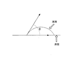
相対表面エネルギーの測定方法の1つは、層上で特定の液体の接触角を比較することである。本明細書において使用される場合、用語「接触角」は、図1に示される角度Φを意味することを意図している。液体媒体の液滴の場合、角度Φは、表面の面と、液滴の外側端部から表面までの線との交差部分によって定義される。さらに、角度Φは、液滴が適用された後で表面上で平衡位置に達した後で測定され、すなわち「静的接触角」である。さまざまな製造者が、接触角を測定可能な装置を製造している。 One method of measuring relative surface energy is to compare the contact angles of specific liquids on the layers. As used herein, the term “contact angle” is intended to mean the angle Φ shown in FIG. For liquid medium droplets, the angle Φ is defined by the intersection of the surface plane and the line from the outer edge of the droplet to the surface. Furthermore, the angle Φ is measured after reaching the equilibrium position on the surface after the droplet has been applied, ie the “static contact angle”. Various manufacturers produce devices that can measure contact angles.
ある実施形態においては、第1の表面エネルギーは十分高く、多くの従来の溶媒によってぬらすことができる。ある実施形態においては、第1の層は、フェニルヘキサンでぬらすことができ、40°以下の接触角を有する。 In some embodiments, the first surface energy is sufficiently high and can be wetted by many conventional solvents. In some embodiments, the first layer can be wetted with phenyl hexane and has a contact angle of 40 ° or less.
中間層は、第1の表面エネルギーよりも低い第2の表面エネルギーを有する。ある実施形態においては、中間層は、フェニルヘキサンでぬらすことはできず、少なくとも70°の接触角を有する。 The intermediate layer has a second surface energy that is lower than the first surface energy. In some embodiments, the interlayer cannot be wetted with phenyl hexane and has a contact angle of at least 70 °.
一実施形態においては、中間層はフッ素化材料を含む。一実施形態においては、中間層は、パーフルオロアルキルエーテル基を有する材料を含む。一実施形態においては、このフルオロアルキル基は2〜20個の炭素原子を有する。一実施形態においては、中間層は、パーフルオロアルキルエーテルペンダント側鎖を有するフッ素化アルキレン主鎖を含む。 In one embodiment, the intermediate layer includes a fluorinated material. In one embodiment, the intermediate layer includes a material having perfluoroalkyl ether groups. In one embodiment, the fluoroalkyl group has 2-20 carbon atoms. In one embodiment, the intermediate layer comprises a fluorinated alkylene backbone having perfluoroalkyl ether pendant side chains.
一実施形態においては、中間層はフッ素化酸を含む。一実施形態においては、このフッ素化酸はオリゴマーである。一実施形態においては、このオリゴマーは、フッ素化オレフィン主鎖と、フッ素化エーテルスルホネート、フッ素化エステルスルホネート、またはフッ素化エーテルスルホンイミドのペンダント基とを有する。一実施形態においては、フッ素化酸は、1,1−ジフルオロエチレンと、2−(1,1−ジフルオロ−2−(トリフルオロメチル)アリルオキシ)−1,1,2,2−テトラフルオロエタンスルホン酸とのオリゴマーである。一実施形態においては、フッ素化酸は、エチレンと、2−(2−(1,2,2−トリフルオロビニルオキシ)−1,1,2,3,3,3−ヘキサフルオロプロポキシ)−1,1,2,2−テトラフルオロエタンスルホン酸とのオリゴマーである。これらのオリゴマーは、対応するフッ化スルホニルオリゴマーとして製造され、続いてスルホン酸形態に変換することができる。一実施形態においては、フッ素化酸ポリマーは、フッ素化および部分スルホン化ポリ(アリーレンエーテルスルホン)のオリゴマーである。 In one embodiment, the intermediate layer includes a fluorinated acid. In one embodiment, the fluorinated acid is an oligomer. In one embodiment, the oligomer has a fluorinated olefin backbone and pendant groups of fluorinated ether sulfonate, fluorinated ester sulfonate, or fluorinated ether sulfonimide. In one embodiment, the fluorinated acid is 1,1-difluoroethylene and 2- (1,1-difluoro-2- (trifluoromethyl) allyloxy) -1,1,2,2-tetrafluoroethanesulfone. Oligomer with acid. In one embodiment, the fluorinated acid is ethylene and 2- (2- (1,2,2-trifluorovinyloxy) -1,1,2,3,3,3-hexafluoropropoxy) -1 , 1,2,2-tetrafluoroethanesulfonic acid oligomer. These oligomers can be produced as the corresponding sulfonyl fluoride oligomers and subsequently converted to the sulfonic acid form. In one embodiment, the fluorinated acid polymer is an oligomer of fluorinated and partially sulfonated poly (arylene ether sulfone).
(3.方法)
本明細書において提供される方法では、第1の層が形成され中間層が第1の層上に形成され、中間層の選択された部分が除去されてパターン化された中間層と第1の層の非被覆領域とが形成され、閉じ込められた第2の層が第1の層の非被覆領域上に形成される。
(3. Method)
In the method provided herein, a first layer is formed, an intermediate layer is formed on the first layer, selected portions of the intermediate layer are removed, and the patterned intermediate layer and the first layer An uncovered region of the layer is formed, and a confined second layer is formed on the uncovered region of the first layer.
一実施形態においては、第1の層は基体である。この基体は無機であっても有機であってもよい。基体の例としては、ガラス、セラミック、およびポリエステルフィルムやポリイミドフィルムなどのポリマーフィルムが挙げられるが、これらに限定されるものではない。 In one embodiment, the first layer is a substrate. This substrate may be inorganic or organic. Examples of the substrate include, but are not limited to, glass, ceramic, and polymer films such as polyester film and polyimide film.
一実施形態においては、第1の層は電極である。この電極は、パターン化されない場合もあるし、パターン化される場合もある。一実施形態においては、この電極は、平行なラインでパターン化される。この電極は基体上に存在することができる。 In one embodiment, the first layer is an electrode. This electrode may or may not be patterned. In one embodiment, the electrodes are patterned with parallel lines. This electrode can be present on the substrate.
一実施形態においては、第1の層が基体上に堆積される。第1の層は、パターン化されない場合もあるし、パターン化される場合もある。一実施形態においては、第1の層は、電子デバイス中の有機活性層である。 In one embodiment, the first layer is deposited on the substrate. The first layer may be unpatterned or may be patterned. In one embodiment, the first layer is an organic active layer in an electronic device.
第1の層は、気相堆積技術、液相堆積技術、および熱転写技術などのあらゆる堆積技術によって形成することができる。一実施形態においては、第1の層は液相堆積技術によって堆積され、続いて乾燥される。この場合、第1の材料が、液体媒体中に溶解または分散される。液相堆積方法は、連続的であっても不連続であってもよい。連続液相堆積技術としては、スピンコーティング、ロールコーティング、カーテンコーティング、浸漬コーティング、スロットダイコーティング、スプレーコーティング、および連続ノズルコーティングが挙げられるが、これらに限定されるものではない。不連続液相堆積技術としては、インクジェット印刷、グラビア印刷、フレキソ印刷、およびスクリーン印刷が挙げられるが、これらに限定されるものではない。一実施形態においては、第1の層は連続液相堆積技術によって堆積される。第1の材料および下にあるあらゆる材料が損傷しないのであれば、乾燥ステップを室温または高温で行うことができる。 The first layer can be formed by any deposition technique, such as vapor deposition techniques, liquid deposition techniques, and thermal transfer techniques. In one embodiment, the first layer is deposited by a liquid deposition technique followed by drying. In this case, the first material is dissolved or dispersed in the liquid medium. The liquid deposition method may be continuous or discontinuous. Continuous liquid deposition techniques include, but are not limited to, spin coating, roll coating, curtain coating, dip coating, slot die coating, spray coating, and continuous nozzle coating. Discontinuous liquid deposition techniques include, but are not limited to, ink jet printing, gravure printing, flexographic printing, and screen printing. In one embodiment, the first layer is deposited by a continuous liquid deposition technique. If the first material and any underlying material are not damaged, the drying step can be performed at room temperature or elevated temperature.
中間層は、第1の層上に、第1の層に直接接触して形成される。ある実施形態においては、第1の層の実質的にすべてが中間層で覆われる。ある実施形態においては、縁端部および対象の有効領域外の領域は覆われないままで維持される。中間層は、気相堆積技術、液相堆積技術、および熱転写技術などのあらゆる堆積技術によって形成することができる。 The intermediate layer is formed on the first layer and in direct contact with the first layer. In some embodiments, substantially all of the first layer is covered with an intermediate layer. In some embodiments, the edges and areas outside the target effective area are left uncovered. The intermediate layer can be formed by any deposition technique such as vapor deposition techniques, liquid deposition techniques, and thermal transfer techniques.
一実施形態においては、中間層は、化学的または物理的であってよい気相堆積方法によって形成される。 In one embodiment, the intermediate layer is formed by a vapor deposition method that may be chemical or physical.
一実施形態においては、中間層は液相堆積技術によって堆積される。 In one embodiment, the intermediate layer is deposited by a liquid deposition technique.
ある実施形態においては、中間材料は、液体媒体中に溶解または分散される。液相堆積方法は、前述したように連続的であっても不連続であってもよい。中間材料を堆積するための液体媒体の選択は、材料自体の厳密な性質に依存する。一実施形態においては、中間材料はフッ素化材料であり、液体媒体はフッ素化液体である。フッ素化液体の例としては、パーフルオロオクタン、トリフルオロトルエン、およびヘキサフルオロキシレンが挙げられるが、これらに限定されるものではない。第1の層に関して前述したように、液体組成物を堆積した後、その材料を乾燥させて層を形成させる。 In certain embodiments, the intermediate material is dissolved or dispersed in a liquid medium. The liquid deposition method may be continuous or discontinuous as described above. The choice of liquid medium for depositing the intermediate material depends on the exact nature of the material itself. In one embodiment, the intermediate material is a fluorinated material and the liquid medium is a fluorinated liquid. Examples of fluorinated liquids include, but are not limited to perfluorooctane, trifluorotoluene, and hexafluoroxylene. After depositing the liquid composition as described above for the first layer, the material is dried to form the layer.
ある実施形態においては、中間層は液相堆積によって形成されるが、それが液体媒体に加えられることはない。一実施形態においては、中間材料は室温において液体であり、液相堆積によって第1の層上に堆積される。液体中間材料はフィルム形成性である場合もあるし、第1の層の表面上に吸収または吸着される場合もある。一実施形態においては、第1の層上に中間層を形成するために、液体中間材料が、その融点未満の温度まで冷却される。一実施形態においては、中間材料が室温において液体ではなく、その融点を超える温度まで加熱され、第1の層上に堆積され、室温まで冷却することで、中間層が第1の層上に形成される。液相堆積の場合、前述のあらゆる方法を使用することができる。 In some embodiments, the intermediate layer is formed by liquid deposition, but it is not added to the liquid medium. In one embodiment, the intermediate material is liquid at room temperature and is deposited on the first layer by liquid deposition. The liquid intermediate material may be film-forming or may be absorbed or adsorbed on the surface of the first layer. In one embodiment, the liquid intermediate material is cooled to a temperature below its melting point to form an intermediate layer on the first layer. In one embodiment, the intermediate material is not liquid at room temperature, but is heated to a temperature above its melting point, deposited on the first layer, and cooled to room temperature, thereby forming the intermediate layer on the first layer. Is done. For liquid deposition, any of the methods described above can be used.
中間層の厚さは、材料の最終用途に依存しうる。ある実施形態においては、中間層の厚さは少なくとも100Åである。ある実施形態においては、中間層は100〜3000Åの範囲内であり、ある実施形態においては1000〜2000Åの範囲内である。 The thickness of the intermediate layer can depend on the end use of the material. In some embodiments, the thickness of the intermediate layer is at least 100 mm. In some embodiments, the intermediate layer is in the range of 100 to 3000 inches, and in some embodiments in the range of 1000 to 2000 inches.
次に、中間層が処理されることで選択された部分が除去されて、中間材料のパターンが第1の層上に形成される。 The intermediate layer is then processed to remove selected portions and a pattern of intermediate material is formed on the first layer.
一実施形態においては、中間層の選択された部分はフォトレジスト技術を使用して除去される。フォトレジスト技術の使用は当技術分野において周知である。感光性材料の1つであるフォトレジストを、中間層の表面全体の上に堆積する。このフォトレジストを活性化放射線にパターン露光する。次にフォトレジストを現像して、露光部分または未露光部分のいずれかが除去される。ある実施形態においては、可溶性、膨潤性、または分散性がより高いフォトレジストの領域を除去するために溶媒で処理することによって現像が行われる。フォトレジストの領域を除去した後、これによって、被覆されていない中間層の領域が得られる。続いて、制御されたエッチングステップによって、中間層のこれらの領域が除去される。ある実施形態においては、エッチングは、中間層を除去するが下にある第1の層は除去しない溶媒を使用して行うことができる。ある実施形態においては、エッチングはプラズマで処理することによって行うことができる。続いて、通常は溶媒で処理することによって、残りのフォトレジストが除去される。 In one embodiment, selected portions of the intermediate layer are removed using photoresist technology. The use of photoresist technology is well known in the art. A photoresist, one of the photosensitive materials, is deposited over the entire surface of the intermediate layer. The photoresist is pattern exposed to activating radiation. The photoresist is then developed to remove either the exposed or unexposed portions. In some embodiments, development is performed by treatment with a solvent to remove areas of the photoresist that are more soluble, swellable, or dispersible. After removing the areas of the photoresist, this gives areas of the uncoated intermediate layer. Subsequently, these regions of the intermediate layer are removed by a controlled etching step. In some embodiments, the etching can be performed using a solvent that removes the intermediate layer but not the underlying first layer. In some embodiments, the etching can be performed by processing with a plasma. Subsequently, the remaining photoresist is removed, usually by treatment with a solvent.
一実施形態においては、放射線でパターン処理することによって、中間層の選択された部分が除去される。用語「放射する」および「放射」は、このような放射が放射線、波、または粒子のいずれの形態であるかとは無関係に、あらゆる形態の熱、電磁スペクトル全体、または亜原子粒子などのあらゆる形態のエネルギーの適用を意味することを意図している。一実施形態においては、中間層は熱不安定性材料を含み、赤外線で処理することによって一部が除去される。ある実施形態においては、レーザーによって赤外線が照射される。赤外ダイオードレーザーは周知であり、中間層にパターン露光するために使用することができる。一実施形態においては、中間層の一部は、UV線に露光することによって除去することができる。 In one embodiment, selected portions of the intermediate layer are removed by patterning with radiation. The terms “radiate” and “radiation” refer to any form of heat, the entire electromagnetic spectrum, or subatomic particles, regardless of whether such radiation is in the form of radiation, waves, or particles. Is intended to mean the application of energy. In one embodiment, the intermediate layer includes a thermally labile material and is partially removed by treatment with infrared radiation. In some embodiments, infrared radiation is emitted by a laser. Infrared diode lasers are well known and can be used to pattern expose an intermediate layer. In one embodiment, a portion of the intermediate layer can be removed by exposure to UV radiation.
一実施形態においては、中間層の選択された部分はレーザーアブレーションによって除去される。一実施形態においては、エキシマレーザーが使用される。 In one embodiment, selected portions of the intermediate layer are removed by laser ablation. In one embodiment, an excimer laser is used.
一実施形態においては、中間層の選択された部分は、ドライエッチングによって除去される。本明細書において使用される場合、用語「ドライエッチング」は、ガスを使用して行われるエッチングを意味する。ドライエッチングは、イオン化ガスを使用して行うこともできるし、イオン化ガスを使用せずに行うこともできる。一実施形態においては、少なくとも1つの酸素含有ガスが、使用されるガス中に存在する。代表的な酸素含有ガスとしては、O2、COF2、CO、O3、NO、N2O、およびそれらの混合物が挙げられる。少なくとも1つのハロゲン含有ガスを、少なくとも1つの酸素含有ガスとともに使用することもできる。ハロゲン含有ガスは、フッ素含有ガス、塩素含有ガス、臭素含有ガス、またはヨウ素含有ガス、およびそれらの混合物の任意の1つまたは複数を含むことができる。 In one embodiment, selected portions of the intermediate layer are removed by dry etching. As used herein, the term “dry etching” means etching performed using a gas. Dry etching can be performed using an ionized gas, or can be performed without using an ionized gas. In one embodiment, at least one oxygen-containing gas is present in the gas used. Exemplary oxygen-containing gases include O 2 , COF 2 , CO, O 3 , NO, N 2 O, and mixtures thereof. At least one halogen-containing gas can also be used with at least one oxygen-containing gas. The halogen-containing gas can include any one or more of a fluorine-containing gas, a chlorine-containing gas, a bromine-containing gas, or an iodine-containing gas, and mixtures thereof.
続いて、第1の層の非被覆領域上に第2の層が適用される。第2の層は、あらゆる堆積技術によって適用することができる。一実施形態においては、第2の層は液相堆積技術によって適用される。ある実施形態においては、液体媒体中に溶解または分散させた第2の材料を含む液体組成物をパターン化された中間層上に適用し、乾燥させることで第2の層が形成される。この液体組成物は、中間層の表面エネルギーより高いが、第1の層の表面エネルギーとほぼ同じかそれ未満である表面エネルギーを有するように選択される。この液体組成物は、第1の層をぬらすが、中間層からはじかれる。この液体は、中間層の領域上に広がることができるが、非ぬれ性である。このようにして、閉じ込められた第2の層が形成される。 Subsequently, a second layer is applied over the uncovered area of the first layer. The second layer can be applied by any deposition technique. In one embodiment, the second layer is applied by liquid deposition techniques. In some embodiments, the second layer is formed by applying a liquid composition comprising a second material dissolved or dispersed in a liquid medium onto the patterned intermediate layer and drying. The liquid composition is selected to have a surface energy that is higher than the surface energy of the intermediate layer, but approximately equal to or less than the surface energy of the first layer. This liquid composition wets the first layer but is repelled from the intermediate layer. This liquid can spread over the area of the intermediate layer, but is non-wetting. In this way, a confined second layer is formed.
一実施形態においては、第2の層は連続液相堆積技術を使用して適用される。一実施形態においては、第2の層は不連続液相堆積技術を使用して適用される。 In one embodiment, the second layer is applied using a continuous liquid deposition technique. In one embodiment, the second layer is applied using a discontinuous liquid deposition technique.
一実施形態においては、第1の層は、液体閉じ込め構造の上に適用される。完全な閉じ込めには不十分であるが、印刷した層の厚さの均一性は依然として調整可能となる構造を使用することが望ましい場合がある。この場合、厚さ調節構造の上のぬれを制御でき、閉じ込めおよび均一性の両方が得られることが望ましい場合がある。その後、発光インクの接触角を調節できることが望ましい。閉じ込めに使用される大部分の表面処理(たとえば、CF4プラズマ)では、このレベルの制御が行えない。 In one embodiment, the first layer is applied over the liquid confinement structure. It may be desirable to use a structure that is insufficient for complete confinement, but the thickness uniformity of the printed layer is still adjustable. In this case, it may be desirable to be able to control the wetting on the thickness adjusting structure and to obtain both confinement and uniformity. Thereafter, it is desirable that the contact angle of the luminescent ink can be adjusted. Most surface treatments used for confinement (eg, CF4 plasma) do not provide this level of control.
一実施形態においては、第1の層が、いわゆるバンク構造の上に適用される。バンク構造は、典型的にはフォトレジスト、有機材料(たとえば、ポリイミド)、または無機材料(酸化物、窒化物など)から形成される。バンク構造は、液体の形態の第1の層を閉じ込めて色の混合を防止するため、および/または液体の形態から乾燥するときの第1の層の厚さの均一性を改善するため、および/または下にある特徴を液体との接触から保護するために使用することができる。このような下にある特徴としては、導電性トレース、導電性トレース間の間隙、薄膜トランジスタ、電極などを挙げることができる。 In one embodiment, the first layer is applied over a so-called bank structure. The bank structure is typically formed from a photoresist, an organic material (eg, polyimide), or an inorganic material (oxide, nitride, etc.). The bank structure confines the first layer in the liquid form to prevent color mixing and / or improves the uniformity of the thickness of the first layer when drying from the liquid form, and It can be used to protect the underlying features from contact with liquids. Such underlying features can include conductive traces, gaps between conductive traces, thin film transistors, electrodes, and the like.
本明細書において提供される方法の一実施形態においては、第1および第2の層は有機活性層である。第1の有機活性層は第1の電極上に形成され、第1の有機活性層が、層の表面エネルギーを低下させる反応性界面活性組成物で処理され、第2の有機活性層が、処理された第1の有機活性層の上に形成される。 In one embodiment of the method provided herein, the first and second layers are organic active layers. A first organic active layer is formed on the first electrode, the first organic active layer is treated with a reactive surfactant composition that reduces the surface energy of the layer, and the second organic active layer is treated. Formed on the first organic active layer formed.
一実施形態においては、第1の有機活性層は、第1の有機活性材料と液体媒体とを含む液体組成物の液相堆積によって形成される。この液体組成物が第1の電極上に堆積され、続いて乾燥させることで層が形成される。一実施形態においては、第1の有機活性層は、連続液相堆積方法によって形成される。このような方法では、歩留まりが高くなり設備費が低くなる場合がある。 In one embodiment, the first organic active layer is formed by liquid deposition of a liquid composition comprising a first organic active material and a liquid medium. This liquid composition is deposited on the first electrode and subsequently dried to form a layer. In one embodiment, the first organic active layer is formed by a continuous liquid deposition method. In such a method, the yield may be high and the equipment cost may be low.
一実施形態においては、中間層は液体組成物から形成される。この液相堆積方法は、前述のように連続滴であっても不連続であってもよい。一実施形態においては、連続液相堆積方法を使用して中間層液体組成物が堆積される。 In one embodiment, the intermediate layer is formed from a liquid composition. As described above, this liquid phase deposition method may be continuous droplets or discontinuous. In one embodiment, the intermediate layer liquid composition is deposited using a continuous liquid deposition method.
(4.有機電子デバイス)
本発明の方法を、電子デバイスにおける使用に関してさらに説明するが、本発明の方法がそのような使用に限定されるものではない。
(4. Organic electronic devices)
Although the method of the present invention will be further described with respect to use in electronic devices, the method of the present invention is not limited to such use.
図2は、代表的な電子デバイスの有機発光ダイオード(OLED)ディスプレイであり、2つの電気接触層の間に配置された少なくとも2つの有機活性層を含む。電子デバイス100は、アノード層110から光活性層140への正孔の注入を促進するための1つまたは複数の層120および130を含む。一般に、2つの層が存在する場合、アノードに隣接する層120は正孔注入層または緩衝層と呼ばれる。光活性層に隣接する層130は正孔輸送層と呼ばれる。場合により電子輸送層150が光活性層140とカソード層160との間に配置される。デバイス100の用途に依存するが、光活性層140は、印加電圧によって励起する発光層(発光ダイオード中または発光電気化学セル中など)、放射エネルギーに応答し、バイアス電圧の印加を使用してまたは使用せずに信号を発生する材料層(光検出器中など)であってよい。本発明のデバイスは、システム、駆動方法、および利用形態に関しては限定されない。
FIG. 2 is a typical electronic device organic light emitting diode (OLED) display, comprising at least two organic active layers disposed between two electrical contact layers. The
マルチカラーデバイスの場合、光活性層140は、少なくとも3つの異なる色の異なる領域で構成される。異なる色の領域は、別々の着色領域を印刷することによって形成することができる。あるいは、層全体を形成し、異なる色の発光材料を層の異なる領域にドープすることによって形成することができる。このような方法は、たとえば米国特許公報(特許文献1)に記載されている。
In the case of a multicolor device, the
ある実施形態においては、本明細書に記載される新規方法は、有機層(第2の層)を電極層(第1の層)に適用するために使用することができる。一実施形態においては、第1の層がアノード110であり、第2の層が緩衝層120である。
In certain embodiments, the novel method described herein can be used to apply an organic layer (second layer) to an electrode layer (first layer). In one embodiment, the first layer is the
ある実施形態においては、本明細書に記載される新規方法は、デバイス中のあらゆる連続する有機層の組に使用され、第2の層が特定の領域内に閉じ込められる。本発明の新規方法の一実施形態においては、第2の有機活性層が光活性層140であり、第1の有機活性層は、層140の直前に適用されるデバイス層である。多くの場合、デバイスはアノード層から始まって製造される。正孔輸送層130が存在する場合、光活性層140が適用される前に、中間層が層130に適用される。層130が存在しない場合、中間層は層120に適用される。カソードから始まってデバイスが製造される場合、光活性層140が適用される前に、中間層が電子輸送層150に適用される。
In certain embodiments, the novel methods described herein are used for any set of consecutive organic layers in the device, and the second layer is confined within a particular region. In one embodiment of the novel method of the present invention, the second organic active layer is a
本発明の新規方法の一実施形態においては、第2の有機活性層が正孔輸送層130であり、第1の有機活性層は、層130の直前に適用されるデバイス層である。アノード層から始まってデバイスが製造される実施形態においては、正孔輸送層130を適用する前に、緩衝層120に対してRSA処理が行われる。
In one embodiment of the novel method of the present invention, the second organic active layer is a
一実施形態においては、アノード110は平行なストライプのパターンで形成される。緩衝層120、および場合により正孔輸送層130は、アノード110の上に連続層として形成される。中間層は、層130(存在する場合)または層120(層130が存在しない場合)の上に別個の層として直接適用される。少なくともアノードストライプ間の領域は非被覆となるようなパターンで中間層が除去される。ある実施形態においては、アノードストライプの間の領域とアノードストライプの外側端部とが非被覆となる。
In one embodiment, the
デバイス中の他の層は、そのような層が果たすべき機能を考慮することによってそのような層に有用であることが知られているあらゆる材料でできていてよい。本発明のデバイスは、アノード層110またはカソード層150に隣接することができる支持体または基体(図示せず)を含むことができる。ほとんどの場合、支持体はアノード層110に隣接している。支持体は、可撓性の場合も剛性の場合もあるし、有機の場合も無機の場合もある。一般に、ガラスまたは可撓性有機フィルムが支持体として使用される。アノード層110は、カソード層160よりも正孔の注入が効率的な電極である。アノードは、金属、混合金属、合金、金属酸化物、または混合酸化物を含有する材料を含むことができる。好適な材料としては、2族元素(すなわち、Be、Mg、Ca、Sr、Ba、Ra)の混合酸化物、11族元素、4族、5族、および6族の元素、ならびに8〜10族の遷移元素が挙げられる。アノード層110を光透過性にするためには、インジウム・スズ酸化物などの12族、13族、および14族の元素の混合酸化物を使用することができる。本明細書において使用される場合、語句「混合酸化物」は、2族元素、あるいは12族、13族、または14族の元素から選択される2つ以上の異なる陽イオンを有する酸化物を意味する。アノード層110の材料の一部の非限定的な具体例としては、インジウム・スズ酸化物(「ITO」)、インジウム・亜鉛酸化物、アルミニウム・スズ酸化物、金、銀、銅、およびニッケルが挙げられるが、これらに限定されるものではない。アノードは、ポリアニリン、ポリチオフェン、またはポリピロールなどの有機材料を含むこともできる。
The other layers in the device may be made of any material known to be useful for such layers by considering the function that such layers are to perform. The device of the present invention can include a support or substrate (not shown) that can be adjacent to the
アノード層110は、化学蒸着法または物理蒸着法、あるいはスピンキャスト法によって形成することができる。化学蒸着は、プラズマ化学蒸着(「PECVD」)または金属有機化学蒸着(「MOCVD」)として行うことができる。物理蒸着としては、イオンビームスパッタリングなどのスパッタリング、ならびにeビーム蒸発、および抵抗蒸発のあらゆる形態を挙げることができる。物理蒸着の具体的な形態としては、高周波マグネトロンスパッタリング、および誘導結合プラズマ物理蒸着(「IMP−PVD」)が挙げられる。これらの堆積技術は、半導体製造分野においては周知である。
The
通常、アノード層110は、リソグラフィ作業中にパターン化される。このパターンは、希望に応じて変更することができる。これらの層は、第1の電気接触層材料を適用する前に、第1の可撓性複合バリア構造上にパターンニングされたマスクまたはレジストを配置することなどによってパターンを形成することができる。あるいは、これらの層は、全体の層として適用することができ(ブランケット堆積とも呼ばれる)、続いて、たとえば、パターン化されたレジスト層と湿式化学エッチングまたはドライエッチング技術とを使用してパターン化することができる。当技術分野において周知の他のパターニング方法を使用することもできる。電子デバイスがアレイ内に配置される場合、典型的にはアノード層110は、実質的に同方向に延在する長さを有する実質的に平行なストリップに成形される。
Typically, the
緩衝層120は、光活性層中への正孔の注入を促進し、デバイス中の短絡を防止するためにアノード表面を滑らかにする機能を果たす。典型的には緩衝層は、プロトン酸がドープされることが多いポリアニリン(PANI)またはポリエチレンジオキシチオフェン(PEDOT)などのポリマー材料で形成される。プロトン酸は、たとえば、ポリ(スチレンスルホン酸)、ポリ(2−アクリルアミド−2−メチル−1−プロパンスルホン酸)などであってよい。緩衝層120は、銅フタロシアニンやテトラチアフルバレン−テトラシアノキノジメタン系(TTF−TCNQ)などの電荷輸送化合物などを含むことができる。一実施形態においては、緩衝層120は、導電性ポリマーとコロイド形成性ポリマー酸との分散体から作製される。このような材料は、たとえば、米国特許公報(特許文献2)および米国特許公報(特許文献3)に記載されている。
The
緩衝層120はあらゆる堆積技術によって適用することができる。一実施形態においては、この緩衝層は、前述のような溶液堆積法によって適用される。一実施形態においては、この緩衝層は連続溶液堆積法によって適用される。
The
任意選択の層130の正孔輸送材料の例は、たとえば、(非特許文献3)にまとめられている。正孔輸送分子および正孔輸送ポリマーの両方を使用することができる。一般に使用される正孔輸送分子としては:4,4’,4”−トリス(N,N−ジフェニル−アミノ)−トリフェニルアミン(TDATA);4,4’,4”−トリス(N−3−メチルフェニル−N−フェニル−アミノ)−トリフェニルアミン(MTDATA);N,N’−ジフェニル−N,N’−ビス(3−メチルフェニル)−[1,1’−ビフェニル]−4,4’−ジアミン(TPD);1,1−ビス[(ジ−4−トリルアミノ)フェニル]シクロヘキサン(TAPC);N,N’−ビス(4−メチルフェニル)−N,N’−ビス(4−エチルフェニル)−[1,1’−(3,3’−ジメチル)ビフェニル]−4,4’−ジアミン(ETPD);テトラキス−(3−メチルフェニル)−N,N,N’,N’−2,5−フェニレンジアミン(PDA);α−フェニル−4−N,N−ジフェニルアミノスチレン(TPS);p−(ジエチルアミノ)−ベンズアルデヒドジフェニルヒドラゾン(DEH);トリフェニルアミン(TPA);ビス[4−(N,N−ジエチルアミノ)−2−メチルフェニル](4−メチルフェニル)メタン(MPMP);1−フェニル−3−[p−(ジエチルアミノ)スチリル]−5−[p−(ジエチルアミノ)フェニル]ピラゾリン(PPRまたはDEASP);1,2−trans−ビス(9H−カルバゾール−9−イル)シクロブタン(DCZB);N,N,N’,N’−テトラキス(4−メチルフェニル)−(1,1’−ビフェニル)−4,4’−ジアミン(TTB);N,N’−ビス(ナフタレン−1−イル)−N,N’−ビス−(フェニル)ベンジジン(α−NPB);および銅フタロシアニンなどのポルフィリン系化合物が挙げられるがこれらに限定されるものではない。一般に使用される正孔輸送ポリマーとしては、限定するものではないが、ポリビニルカルバゾール、(フェニルメチル)ポリシラン、ポリ(ジオキシチオフェン)、ポリアニリン、およびポリピロールが挙げられる。ポリスチレンやポリカーボネートなどのポリマー中に上述のものなどの正孔輸送分子をドープすることによって正孔輸送ポリマーを得ることもできる。ある実施形態においては、正孔輸送材料は、架橋性のオリゴマー材料またはポリマー材料を含む。正孔輸送層を形成した後、材料を放射線で処理することで架橋させる。ある実施形態においては、放射線が熱放射である。
Examples of hole transport materials for
正孔輸送層130は、あらゆる堆積技術によって適用することができる。一実施形態においては、正孔輸送層は、前述のような溶液堆積法によって適用される。一実施形態においては、正孔輸送層は連続溶液堆積法によって適用される。
The
限定するものではないが、小分子有機蛍光化合物、蛍光性およびリン光性の金属錯体、共役ポリマー、およびそれらの混合物などのあらゆる有機エレクトロルミネッセンス(「EL」)材料を、光活性層140中に使用することができる。蛍光化合物の例としては、ピレン、ペリレン、ルブレン、クマリン、それらの誘導体、およびそれらの混合物が挙げられるが、これらに限定されるものではない。金属錯体の例としては、トリス(8−ヒドロキシキノラト)アルミニウム(Alq3)などの金属キレート化オキシノイド化合物;ペトロフ(Petrov)らの米国特許公報(特許文献4)、ならびに(特許文献5)および(特許文献6)に開示されるような、フェニルピリジン配位子、フェニルキノリン配位子、またはフェニルピリミジン配位子を有するイリジウムの錯体などのシクロメタレート化イリジウムおよび白金エレクトロルミネッセンス化合物、ならびに、たとえば、(特許文献7)、(特許文献8)、および(特許文献9)に記載されているような有機金属錯体、ならびにそれらの混合物が挙げられるが、これらに限定されるものではない。電荷輸送ホスト材料と金属錯体とを含むエレクトロルミネッセンス発光層が、トンプソン(Thompson)らによる米国特許公報(特許文献10)、ならびにバローズ(Burrows)およびトンプソン(Thompson)による(特許文献11)および(特許文献12)に記載されている。共役ポリマーの例としては、ポリ(フェニレンビニレン)、ポリフルオレン、ポリ(スピロビフルオレン)、ポリチオフェン、ポリ(p−フェニレン)、それらのコポリマー、およびそれらの混合物が挙げられるが、これらに限定されるものではない。
Any organic electroluminescent ("EL") material such as, but not limited to, small molecule organic fluorescent compounds, fluorescent and phosphorescent metal complexes, conjugated polymers, and mixtures thereof can be incorporated into
光活性層140は、あらゆる堆積技術によって適用することができる。一実施形態においては、光活性層は、前述のような溶液堆積法によって。一実施形態においては、光活性層は連続溶液堆積法によって適用される。
The
任意選択の層150は、電子の注入/輸送の両方を促進する機能を果たす場合もあるし、層界面における消光反応を防止する閉じ込め層として機能する場合もある。より具体的には、層150は、電子の移動を促進し、この層がなければ層140および160が直接接触する場合の消光反応の可能性を減少させることができる。任意選択の層150の材料の例としては、金属キレート化オキシノイド化合物(たとえば、Alq3など);フェナントロリン系化合物(たとえば、2,9−ジメチル−4,7−ジフェニル−1,10−フェナントロリン(「DDPA」)、4,7−ジフェニル−1,10−フェナントロリン(「DPA」)など);アゾール化合物(たとえば、2−(4−ビフェニリル)−5−(4−t−ブチルフェニル)−1,3,4−オキサジアゾール(「PBD」など)、3−(4−ビフェニリル)−4−フェニル−5−(4−t−ブチルフェニル)−1,2,4−トリアゾール(「TAZ」など);他の類似の化合物;ならびにそれらの1つまたは複数のあらゆる組み合わせが挙げられるが、これらに限定されるものではない。あるいは、任意選択の層150は無機であってよく、BaO、LiF、Li2Oなどを含むことができる。
Optional layer 150 may serve to promote both electron injection / transport, or may serve as a confinement layer that prevents quenching reactions at the layer interface. More specifically, layer 150 can facilitate electron transfer and reduce the potential for quenching reactions when
カソード層160は、電子または負電荷キャリアの注入に特に有効な電極である。カソード層160は、第1の電気接触層(この場合、アノード層110)よりも低い仕事関数を有するあらゆる金属または非金属であってよい。一実施形態においては、用語「低い仕事関数」は、約4.4eV以下の仕事関数を有する材料を意味することを意図している。一実施形態においては、「高い仕事関数」は、少なくとも約4.4eVの仕事関数を有する材料を意味することを意図している。
The
カソード層の材料は、1族のアルカリ金属(たとえば、Li、Na、K、Rb、Cs,)、2族金属(たとえば、Mg、Ca、Baなど)、12族金属、ランタニド(たとえば、Ce、Sm、Euなど)、およびアクチニド(たとえば、Th、Uなど)から選択することができる。アルミニウム、インジウム、イットリウム、およびそれらの組み合わせなどの材料を使用することもできる。カソード層160の材料の非限定的な具体例としては、バリウム、リチウム、セリウム、セシウム、ユウロピウム、ルビジウム、イットリウム、マグネシウム、サマリウム、ならびにそれらの合金および組み合わせが挙げられるが、これらに限定されるものではない。
The material of the cathode layer is a group 1 alkali metal (eg, Li, Na, K, Rb, Cs,), a group 2 metal (eg, Mg, Ca, Ba, etc.), a group 12 metal, a lanthanide (eg, Ce, Sm, Eu, etc.), and actinides (eg, Th, U, etc.). Materials such as aluminum, indium, yttrium, and combinations thereof can also be used. Non-limiting specific examples of
通常、カソード層160は、化学蒸着法または物理蒸着法によって形成される。
In general, the
別の実施形態においては、追加層が有機電子デバイス内に存在することができる。 In another embodiment, additional layers can be present in the organic electronic device.
デバイスがアノード側から始まって製造される場合、本明細書に記載の新規方法の中間層は、アノード110の形成後、緩衝層120の形成後、正孔輸送層130の後、またはそれらのあらゆる組み合わせで行うことができる。デバイスがカソード側から始まって製造される場合、本明細書に記載の新規方法の中間層は、カソード160の形成後、電子輸送層150の形成後、またはそれらのあらゆる組み合わせで行うことができる。
If the device is manufactured starting from the anode side, the intermediate layer of the novel method described herein can be used after formation of the
種々の層はあらゆる好適な厚さを有することができる。無機アノード層110は通常約500nm以下、たとえば約10〜200nmであり;緩衝層120および正孔輸送層130はそれぞれ通常約250nm以下、たとえば約50〜200nmであり;光活性層140は通常約1000nm以下、たとえば約50〜80nmであり;任意選択の層150は通常約100nm以下、たとえば約20〜80nmであり;カソード層160は通常約100nm以下、たとえば約1〜50nmである。アノード層110またはカソード層160が少なくとも一部の光を透過する必要がある場合、そのような層の厚さは約100nmを超えないほうがよい。
The various layers can have any suitable thickness.
本明細書に記載される概念を以下の実施例でさらに説明するが、特許請求の範囲に記載される本発明の範囲がこれらの実施例によって限定されるものではない。 The concepts described herein will be further described in the following examples, which do not limit the scope of the invention described in the claims.
概要または実施例において前述したすべての行為が必要なわけではなく、特定の行為の一部は不要である場合があり、1つまたは複数のさらに別の行為が、前述の行為に加えて実施される場合があることに留意されたい。さらに、行為が列挙されている順序は、必ずしもそれらが実施される順序ではない。 Not all acts described above in the summary or example are required and some of the specific acts may not be necessary, and one or more additional actions may be performed in addition to the actions described above. Please note that there may be cases. Further, the order in which actions are listed are not necessarily the order in which they are performed.
以上の明細書において、具体的な実施形態を参照しながら本発明の概念を説明してきた。しかし、当業者であれば、特許請求の範囲に記載される本発明の範囲から逸脱せずに種々の修正および変更を行えることが理解できよう。したがって、本明細書および図面は、限定的な意味ではなく説明的なものであると見なすべきであり、すべてのこのような修正は本発明の範囲内に含まれることを意図している。 In the foregoing specification, the concepts of the invention have been described with reference to specific embodiments. However, one of ordinary skill in the art appreciates that various modifications and changes can be made without departing from the scope of the present invention as set forth in the claims below. The specification and drawings are, accordingly, to be regarded in an illustrative rather than a restrictive sense, and all such modifications are intended to be included within the scope of the invention.
特定の実施形態に関して、利益、その他の利点、および問題に対する解決法を以上に記載してきた。しかし、これらの利益、利点、問題の解決法、ならびに、なんらかの利益、利点、または解決法を発生させたり、より顕著にしたりすることがある、あらゆる特徴が、特許請求の範囲のいずれかまたはすべての重要、必要、または本質的な特徴であるとして解釈すべきではない。 Benefits, other advantages, and solutions to problems have been described above with regard to specific embodiments. However, any or all of these benefits, advantages, solutions to problems, and any features that may generate or make any benefit, advantage, or solution appear to be any or all of the claims Should not be construed as an important, necessary, or essential feature of.
別々の実施形態の状況において、明確にするために本明細書に記載されている特定の複数の特徴は、1つの実施形態の中で組み合わせても提供できることを理解されたい。逆に、簡潔にするため1つの実施形態の状況において説明した種々の特徴も、別々に提供したり、あらゆる副次的な組み合わせで提供したりすることができる。さらに、ある範囲において記載される値への言及は、その範囲内にあるすべての値を含んでいる。 It should be understood that in the context of separate embodiments, the specific features described herein for clarity may be provided in combination in one embodiment. Conversely, the various features described in the context of one embodiment for the sake of brevity can also be provided separately or in any sub-combination. Further, reference to values stated in a range include all values within that range.
Claims (19)
第1の表面エネルギーを有する前記第1の層を形成するステップと;
前記第1の層上に、前記第1の層に直接接触する中間層を形成するステップであって、前記中間層が、前記第1の表面エネルギーよりも低い第2の表面エネルギーを有するステップと;
前記中間層の選択された部分を除去して、前記第1の層の非被覆領域と前記第1の層の被覆領域とを含むパターンを形成するステップと;
閉じ込められた第2の層を前記第1の層の前記非被覆領域上に形成するステップと
を含むことを特徴とする方法。 A method of forming a confined second layer on a first layer comprising:
Forming the first layer having a first surface energy;
Forming an intermediate layer on the first layer in direct contact with the first layer, wherein the intermediate layer has a second surface energy lower than the first surface energy; ;
Removing a selected portion of the intermediate layer to form a pattern including an uncovered area of the first layer and a covered area of the first layer;
Forming a confined second layer on the uncovered region of the first layer.
第1の表面エネルギーを有する前記第1の有機活性層を前記電極上に形成するステップと
前記第1の層上に、前記第1の層に直接接触する中間層を形成するステップであって、前記中間層が、前記第1の表面エネルギーよりも低い第2の表面エネルギーを有するステップと;
前記中間層の選択された部分を除去して、前記第1の層の非被覆領域と前記第1の層の被覆領域とを含むパターンを形成するステップと;
閉じ込められた第2の層を前記第1の層の前記非被覆領域上に形成するステップと
を含むことを特徴とする方法。 A method of manufacturing an organic electronic device comprising a first organic active layer and a second organic active layer disposed on an electrode,
Forming the first organic active layer having a first surface energy on the electrode; and forming an intermediate layer on the first layer in direct contact with the first layer, The intermediate layer has a second surface energy lower than the first surface energy;
Removing a selected portion of the intermediate layer to form a pattern including an uncovered area of the first layer and a covered area of the first layer;
Forming a confined second layer on the uncovered region of the first layer.
Applications Claiming Priority (2)
| Application Number | Priority Date | Filing Date | Title |
|---|---|---|---|
| US81093906P | 2006-06-05 | 2006-06-05 | |
| PCT/US2007/013286 WO2007145978A1 (en) | 2006-06-05 | 2007-06-05 | Process for making contained layers and devices made with same |
Publications (2)
| Publication Number | Publication Date |
|---|---|
| JP2009540506A true JP2009540506A (en) | 2009-11-19 |
| JP2009540506A5 JP2009540506A5 (en) | 2011-09-29 |
Family
ID=38657382
Family Applications (1)
| Application Number | Title | Priority Date | Filing Date |
|---|---|---|---|
| JP2009514349A Pending JP2009540506A (en) | 2006-06-05 | 2007-06-05 | Method for manufacturing confinement layer and device manufactured using the same |
Country Status (5)
| Country | Link |
|---|---|
| US (1) | US20080087882A1 (en) |
| EP (1) | EP2025017A1 (en) |
| JP (1) | JP2009540506A (en) |
| TW (1) | TW200849686A (en) |
| WO (1) | WO2007145978A1 (en) |
Families Citing this family (6)
| Publication number | Priority date | Publication date | Assignee | Title |
|---|---|---|---|---|
| US20080286487A1 (en) * | 2007-05-18 | 2008-11-20 | Lang Charles D | Process for making contained layers |
| KR20100094475A (en) | 2007-10-26 | 2010-08-26 | 이 아이 듀폰 디 네모아 앤드 캄파니 | Process and materials for making contained layers and devices made with same |
| KR101995369B1 (en) | 2008-04-03 | 2019-07-02 | 삼성 리서치 아메리카 인코포레이티드 | Light-emitting device including quantum dots |
| WO2011044391A1 (en) * | 2009-10-07 | 2011-04-14 | Qd Vision, Inc. | Device including quantum dots |
| US9525148B2 (en) | 2008-04-03 | 2016-12-20 | Qd Vision, Inc. | Device including quantum dots |
| CN102470660B (en) * | 2009-07-27 | 2014-11-19 | E.I.内穆尔杜邦公司 | Process and materials for making contained layers and devices made with same |
Citations (8)
| Publication number | Priority date | Publication date | Assignee | Title |
|---|---|---|---|---|
| JP2002148821A (en) * | 2000-11-14 | 2002-05-22 | Shin Etsu Chem Co Ltd | Resist surface treating agent composition and pattern forming method |
| WO2003011974A1 (en) * | 2001-07-26 | 2003-02-13 | Nissan Chemical Industries, Ltd. | Polyamic acid resin composition |
| JP2003045672A (en) * | 2001-07-20 | 2003-02-14 | Osram Opto Semiconductors Gmbh | Structure defining material for organic light emitting device |
| JP2004071286A (en) * | 2002-08-05 | 2004-03-04 | Dainippon Printing Co Ltd | Manufacturing method of electroluminescent element |
| JP2004531598A (en) * | 2001-03-09 | 2004-10-14 | スリーエム イノベイティブ プロパティズ カンパニー | Water / oil repellency-imparting ester oligomer containing a perfluoroalkyl moiety |
| JP2005062356A (en) * | 2003-08-08 | 2005-03-10 | Seiko Epson Corp | Method for forming pattern, method for forming wiring pattern, electro-optic apparatus and electronic appliance |
| WO2005031889A2 (en) * | 2003-09-24 | 2005-04-07 | E.I. Dupont De Nemours And Company | Method for the application of active materials onto active surfaces and devices made with such methods |
| JP2005166645A (en) * | 2003-11-14 | 2005-06-23 | Asahi Glass Co Ltd | Forming method of barrier rib for image display element |
Family Cites Families (8)
| Publication number | Priority date | Publication date | Assignee | Title |
|---|---|---|---|---|
| JPH09203803A (en) * | 1996-01-25 | 1997-08-05 | Asahi Glass Co Ltd | Production of color filter and liquid crystal display element formed by using the color filter |
| US6303238B1 (en) * | 1997-12-01 | 2001-10-16 | The Trustees Of Princeton University | OLEDs doped with phosphorescent compounds |
| CA2394886C (en) * | 1999-12-21 | 2012-07-17 | Plastic Logic Limited | Inkjet-fabricated integrated circuits |
| US6670645B2 (en) * | 2000-06-30 | 2003-12-30 | E. I. Du Pont De Nemours And Company | Electroluminescent iridium compounds with fluorinated phenylpyridines, phenylpyrimidines, and phenylquinolines and devices made with such compounds |
| US7098060B2 (en) * | 2002-09-06 | 2006-08-29 | E.I. Du Pont De Nemours And Company | Methods for producing full-color organic electroluminescent devices |
| CA2499364A1 (en) * | 2002-09-24 | 2004-04-08 | E. I. Du Pont De Nemours And Company | Water dispersible polyanilines made with polymeric acid colloids for electronics applications |
| WO2004029128A2 (en) * | 2002-09-24 | 2004-04-08 | E.I. Du Pont De Nemours And Company | Water dispersible polythiophenes made with polymeric acid colloids |
| US6992326B1 (en) * | 2004-08-03 | 2006-01-31 | Dupont Displays, Inc. | Electronic device and process for forming same |
-
2007
- 2007-06-05 US US11/758,269 patent/US20080087882A1/en not_active Abandoned
- 2007-06-05 JP JP2009514349A patent/JP2009540506A/en active Pending
- 2007-06-05 EP EP07795782A patent/EP2025017A1/en not_active Withdrawn
- 2007-06-05 WO PCT/US2007/013286 patent/WO2007145978A1/en active Application Filing
- 2007-06-06 TW TW096120415A patent/TW200849686A/en unknown
Patent Citations (8)
| Publication number | Priority date | Publication date | Assignee | Title |
|---|---|---|---|---|
| JP2002148821A (en) * | 2000-11-14 | 2002-05-22 | Shin Etsu Chem Co Ltd | Resist surface treating agent composition and pattern forming method |
| JP2004531598A (en) * | 2001-03-09 | 2004-10-14 | スリーエム イノベイティブ プロパティズ カンパニー | Water / oil repellency-imparting ester oligomer containing a perfluoroalkyl moiety |
| JP2003045672A (en) * | 2001-07-20 | 2003-02-14 | Osram Opto Semiconductors Gmbh | Structure defining material for organic light emitting device |
| WO2003011974A1 (en) * | 2001-07-26 | 2003-02-13 | Nissan Chemical Industries, Ltd. | Polyamic acid resin composition |
| JP2004071286A (en) * | 2002-08-05 | 2004-03-04 | Dainippon Printing Co Ltd | Manufacturing method of electroluminescent element |
| JP2005062356A (en) * | 2003-08-08 | 2005-03-10 | Seiko Epson Corp | Method for forming pattern, method for forming wiring pattern, electro-optic apparatus and electronic appliance |
| WO2005031889A2 (en) * | 2003-09-24 | 2005-04-07 | E.I. Dupont De Nemours And Company | Method for the application of active materials onto active surfaces and devices made with such methods |
| JP2005166645A (en) * | 2003-11-14 | 2005-06-23 | Asahi Glass Co Ltd | Forming method of barrier rib for image display element |
Also Published As
| Publication number | Publication date |
|---|---|
| TW200849686A (en) | 2008-12-16 |
| WO2007145978A1 (en) | 2007-12-21 |
| US20080087882A1 (en) | 2008-04-17 |
| EP2025017A1 (en) | 2009-02-18 |
Similar Documents
| Publication | Publication Date | Title |
|---|---|---|
| KR101391082B1 (en) | Process for making contained layers and devices made with same | |
| JP5871949B2 (en) | Confinement layer and methods and materials for manufacturing devices manufactured using the same | |
| US9306185B2 (en) | Process and materials for making contained layers and devices made with same | |
| JP2009533251A5 (en) | ||
| JP5727368B2 (en) | Apparatus and method for vapor phase coating in electronic devices | |
| US20130087779A1 (en) | Process and materials for making contained layers and devices made with same | |
| JP5457337B2 (en) | Method for manufacturing confinement layer | |
| JP2015062900A (en) | Method of forming electroactive layer | |
| JP5701782B2 (en) | Method for forming electroactive layer | |
| JP2009540506A (en) | Method for manufacturing confinement layer and device manufactured using the same | |
| US20130323880A1 (en) | Process and materials for making contained layers and devices made with same | |
| JP2013048118A (en) | Process for making contained layers, and devices made through such process | |
| US20110260137A1 (en) | Process for making contained layers and devices made with same |
Legal Events
| Date | Code | Title | Description |
|---|---|---|---|
| A621 | Written request for application examination |
Free format text: JAPANESE INTERMEDIATE CODE: A621 Effective date: 20100607 |
|
| A521 | Request for written amendment filed |
Free format text: JAPANESE INTERMEDIATE CODE: A523 Effective date: 20110810 |
|
| A977 | Report on retrieval |
Free format text: JAPANESE INTERMEDIATE CODE: A971007 Effective date: 20120111 |
|
| A131 | Notification of reasons for refusal |
Free format text: JAPANESE INTERMEDIATE CODE: A131 Effective date: 20120113 |
|
| A601 | Written request for extension of time |
Free format text: JAPANESE INTERMEDIATE CODE: A601 Effective date: 20120413 |
|
| A602 | Written permission of extension of time |
Free format text: JAPANESE INTERMEDIATE CODE: A602 Effective date: 20120420 |
|
| A521 | Request for written amendment filed |
Free format text: JAPANESE INTERMEDIATE CODE: A523 Effective date: 20120509 |
|
| A131 | Notification of reasons for refusal |
Free format text: JAPANESE INTERMEDIATE CODE: A131 Effective date: 20120622 |
|
| A521 | Request for written amendment filed |
Free format text: JAPANESE INTERMEDIATE CODE: A523 Effective date: 20120921 |
|
| A02 | Decision of refusal |
Free format text: JAPANESE INTERMEDIATE CODE: A02 Effective date: 20130510 |