JP2009503889A - Damage-free ashing process and system after low dielectric constant film etching - Google Patents
Damage-free ashing process and system after low dielectric constant film etching Download PDFInfo
- Publication number
- JP2009503889A JP2009503889A JP2008524962A JP2008524962A JP2009503889A JP 2009503889 A JP2009503889 A JP 2009503889A JP 2008524962 A JP2008524962 A JP 2008524962A JP 2008524962 A JP2008524962 A JP 2008524962A JP 2009503889 A JP2009503889 A JP 2009503889A
- Authority
- JP
- Japan
- Prior art keywords
- containing gas
- dielectric layer
- plasma processing
- substrate
- plasma
- Prior art date
- Legal status (The legal status is an assumption and is not a legal conclusion. Google has not performed a legal analysis and makes no representation as to the accuracy of the status listed.)
- Pending
Links
- 238000000034 method Methods 0.000 title claims abstract description 123
- 230000008569 process Effects 0.000 title claims abstract description 81
- 238000005530 etching Methods 0.000 title claims abstract description 62
- 238000004380 ashing Methods 0.000 title abstract description 6
- 239000000758 substrate Substances 0.000 claims abstract description 66
- 229910002091 carbon monoxide Inorganic materials 0.000 claims abstract description 33
- 229910052760 oxygen Inorganic materials 0.000 claims abstract description 26
- 239000001301 oxygen Substances 0.000 claims abstract description 24
- QVGXLLKOCUKJST-UHFFFAOYSA-N atomic oxygen Chemical compound [O] QVGXLLKOCUKJST-UHFFFAOYSA-N 0.000 claims abstract description 23
- 239000001257 hydrogen Substances 0.000 claims abstract description 21
- 229910052739 hydrogen Inorganic materials 0.000 claims abstract description 21
- UFHFLCQGNIYNRP-UHFFFAOYSA-N Hydrogen Chemical compound [H][H] UFHFLCQGNIYNRP-UHFFFAOYSA-N 0.000 claims abstract description 15
- 239000007789 gas Substances 0.000 claims description 99
- 238000012545 processing Methods 0.000 claims description 74
- QJGQUHMNIGDVPM-UHFFFAOYSA-N nitrogen group Chemical group [N] QJGQUHMNIGDVPM-UHFFFAOYSA-N 0.000 claims description 12
- 229910004298 SiO 2 Inorganic materials 0.000 claims description 11
- 230000008859 change Effects 0.000 claims description 9
- 239000011261 inert gas Substances 0.000 claims description 4
- 230000015572 biosynthetic process Effects 0.000 claims description 3
- 229910052756 noble gas Inorganic materials 0.000 claims description 3
- 229910052581 Si3N4 Inorganic materials 0.000 claims description 2
- 230000008878 coupling Effects 0.000 claims description 2
- 238000010168 coupling process Methods 0.000 claims description 2
- 238000005859 coupling reaction Methods 0.000 claims description 2
- HBMJWWWQQXIZIP-UHFFFAOYSA-N silicon carbide Chemical compound [Si+]#[C-] HBMJWWWQQXIZIP-UHFFFAOYSA-N 0.000 claims description 2
- 229910010271 silicon carbide Inorganic materials 0.000 claims description 2
- HQVNEWCFYHHQES-UHFFFAOYSA-N silicon nitride Chemical compound N12[Si]34N5[Si]62N3[Si]51N64 HQVNEWCFYHHQES-UHFFFAOYSA-N 0.000 claims description 2
- 230000001737 promoting effect Effects 0.000 claims 2
- 239000000463 material Substances 0.000 abstract description 27
- 238000006243 chemical reaction Methods 0.000 abstract description 16
- IJGRMHOSHXDMSA-UHFFFAOYSA-N Atomic nitrogen Chemical compound N#N IJGRMHOSHXDMSA-UHFFFAOYSA-N 0.000 abstract description 15
- 229910052757 nitrogen Inorganic materials 0.000 abstract description 7
- -1 O 2 Chemical compound 0.000 abstract 1
- 239000006227 byproduct Substances 0.000 abstract 1
- 238000002161 passivation Methods 0.000 abstract 1
- 239000010410 layer Substances 0.000 description 65
- UGFAIRIUMAVXCW-UHFFFAOYSA-N Carbon monoxide Chemical compound [O+]#[C-] UGFAIRIUMAVXCW-UHFFFAOYSA-N 0.000 description 25
- QGZKDVFQNNGYKY-UHFFFAOYSA-N Ammonia Chemical compound N QGZKDVFQNNGYKY-UHFFFAOYSA-N 0.000 description 14
- 239000010408 film Substances 0.000 description 11
- 239000004065 semiconductor Substances 0.000 description 9
- 229910021529 ammonia Inorganic materials 0.000 description 7
- CURLTUGMZLYLDI-UHFFFAOYSA-N Carbon dioxide Chemical compound O=C=O CURLTUGMZLYLDI-UHFFFAOYSA-N 0.000 description 6
- VYPSYNLAJGMNEJ-UHFFFAOYSA-N Silicium dioxide Chemical compound O=[Si]=O VYPSYNLAJGMNEJ-UHFFFAOYSA-N 0.000 description 6
- 230000006698 induction Effects 0.000 description 6
- 238000005229 chemical vapour deposition Methods 0.000 description 5
- 238000010586 diagram Methods 0.000 description 5
- 150000002431 hydrogen Chemical class 0.000 description 5
- 239000001307 helium Substances 0.000 description 4
- 229910052734 helium Inorganic materials 0.000 description 4
- SWQJXJOGLNCZEY-UHFFFAOYSA-N helium atom Chemical compound [He] SWQJXJOGLNCZEY-UHFFFAOYSA-N 0.000 description 4
- 238000002347 injection Methods 0.000 description 4
- 239000007924 injection Substances 0.000 description 4
- 230000003287 optical effect Effects 0.000 description 4
- 239000013307 optical fiber Substances 0.000 description 4
- 229920003209 poly(hydridosilsesquioxane) Polymers 0.000 description 4
- 229910002092 carbon dioxide Inorganic materials 0.000 description 3
- 239000001569 carbon dioxide Substances 0.000 description 3
- 238000013461 design Methods 0.000 description 3
- 238000010438 heat treatment Methods 0.000 description 3
- 238000009616 inductively coupled plasma Methods 0.000 description 3
- 238000004519 manufacturing process Methods 0.000 description 3
- 238000000059 patterning Methods 0.000 description 3
- 229920002120 photoresistant polymer Polymers 0.000 description 3
- 238000001020 plasma etching Methods 0.000 description 3
- 239000011148 porous material Substances 0.000 description 3
- 239000010409 thin film Substances 0.000 description 3
- 238000012546 transfer Methods 0.000 description 3
- XKRFYHLGVUSROY-UHFFFAOYSA-N Argon Chemical compound [Ar] XKRFYHLGVUSROY-UHFFFAOYSA-N 0.000 description 2
- XUIMIQQOPSSXEZ-UHFFFAOYSA-N Silicon Chemical compound [Si] XUIMIQQOPSSXEZ-UHFFFAOYSA-N 0.000 description 2
- 238000001816 cooling Methods 0.000 description 2
- 229910001882 dioxygen Inorganic materials 0.000 description 2
- 238000005516 engineering process Methods 0.000 description 2
- 229910052909 inorganic silicate Inorganic materials 0.000 description 2
- 239000011810 insulating material Substances 0.000 description 2
- 239000011229 interlayer Substances 0.000 description 2
- 239000011368 organic material Substances 0.000 description 2
- 238000009832 plasma treatment Methods 0.000 description 2
- 230000005855 radiation Effects 0.000 description 2
- 229910052710 silicon Inorganic materials 0.000 description 2
- 239000010703 silicon Substances 0.000 description 2
- 235000012239 silicon dioxide Nutrition 0.000 description 2
- 239000000377 silicon dioxide Substances 0.000 description 2
- 229910052814 silicon oxide Inorganic materials 0.000 description 2
- 238000001228 spectrum Methods 0.000 description 2
- BSYNRYMUTXBXSQ-UHFFFAOYSA-N Aspirin Chemical compound CC(=O)OC1=CC=CC=C1C(O)=O BSYNRYMUTXBXSQ-UHFFFAOYSA-N 0.000 description 1
- 244000132059 Carica parviflora Species 0.000 description 1
- 235000014653 Carica parviflora Nutrition 0.000 description 1
- PDNNQADNLPRFPG-UHFFFAOYSA-N N.[O] Chemical compound N.[O] PDNNQADNLPRFPG-UHFFFAOYSA-N 0.000 description 1
- 238000013459 approach Methods 0.000 description 1
- 229910052786 argon Inorganic materials 0.000 description 1
- 230000005540 biological transmission Effects 0.000 description 1
- 238000009529 body temperature measurement Methods 0.000 description 1
- 239000000356 contaminant Substances 0.000 description 1
- 239000002826 coolant Substances 0.000 description 1
- 239000010432 diamond Substances 0.000 description 1
- 238000009826 distribution Methods 0.000 description 1
- 230000000694 effects Effects 0.000 description 1
- 238000004993 emission spectroscopy Methods 0.000 description 1
- 238000000295 emission spectrum Methods 0.000 description 1
- 239000000945 filler Substances 0.000 description 1
- 239000011521 glass Substances 0.000 description 1
- 229910052743 krypton Inorganic materials 0.000 description 1
- DNNSSWSSYDEUBZ-UHFFFAOYSA-N krypton atom Chemical compound [Kr] DNNSSWSSYDEUBZ-UHFFFAOYSA-N 0.000 description 1
- 239000004973 liquid crystal related substance Substances 0.000 description 1
- 238000001459 lithography Methods 0.000 description 1
- 239000011159 matrix material Substances 0.000 description 1
- 230000007246 mechanism Effects 0.000 description 1
- 239000012528 membrane Substances 0.000 description 1
- 229910052751 metal Inorganic materials 0.000 description 1
- 239000002184 metal Substances 0.000 description 1
- 125000002496 methyl group Chemical group [H]C([H])([H])* 0.000 description 1
- 238000004377 microelectronic Methods 0.000 description 1
- 238000001393 microlithography Methods 0.000 description 1
- 238000012986 modification Methods 0.000 description 1
- 230000004048 modification Effects 0.000 description 1
- 238000012544 monitoring process Methods 0.000 description 1
- 229910052754 neon Inorganic materials 0.000 description 1
- GKAOGPIIYCISHV-UHFFFAOYSA-N neon atom Chemical compound [Ne] GKAOGPIIYCISHV-UHFFFAOYSA-N 0.000 description 1
- 150000001282 organosilanes Chemical class 0.000 description 1
- 125000005375 organosiloxane group Chemical group 0.000 description 1
- 235000012771 pancakes Nutrition 0.000 description 1
- 238000009931 pascalization Methods 0.000 description 1
- 239000003361 porogen Substances 0.000 description 1
- 238000003672 processing method Methods 0.000 description 1
- 230000001902 propagating effect Effects 0.000 description 1
- 230000003134 recirculating effect Effects 0.000 description 1
- 229920005989 resin Polymers 0.000 description 1
- 239000011347 resin Substances 0.000 description 1
- 230000003595 spectral effect Effects 0.000 description 1
- 239000000126 substance Substances 0.000 description 1
- 238000001392 ultraviolet--visible--near infrared spectroscopy Methods 0.000 description 1
- 229910052724 xenon Inorganic materials 0.000 description 1
- FHNFHKCVQCLJFQ-UHFFFAOYSA-N xenon atom Chemical compound [Xe] FHNFHKCVQCLJFQ-UHFFFAOYSA-N 0.000 description 1
Images


Classifications
-
- H—ELECTRICITY
- H01—ELECTRIC ELEMENTS
- H01L—SEMICONDUCTOR DEVICES NOT COVERED BY CLASS H10
- H01L21/00—Processes or apparatus adapted for the manufacture or treatment of semiconductor or solid state devices or of parts thereof
- H01L21/02—Manufacture or treatment of semiconductor devices or of parts thereof
- H01L21/04—Manufacture or treatment of semiconductor devices or of parts thereof the devices having at least one potential-jump barrier or surface barrier, e.g. PN junction, depletion layer or carrier concentration layer
- H01L21/18—Manufacture or treatment of semiconductor devices or of parts thereof the devices having at least one potential-jump barrier or surface barrier, e.g. PN junction, depletion layer or carrier concentration layer the devices having semiconductor bodies comprising elements of Group IV of the Periodic System or AIIIBV compounds with or without impurities, e.g. doping materials
- H01L21/30—Treatment of semiconductor bodies using processes or apparatus not provided for in groups H01L21/20 - H01L21/26
- H01L21/302—Treatment of semiconductor bodies using processes or apparatus not provided for in groups H01L21/20 - H01L21/26 to change their surface-physical characteristics or shape, e.g. etching, polishing, cutting
- H01L21/306—Chemical or electrical treatment, e.g. electrolytic etching
- H01L21/3065—Plasma etching; Reactive-ion etching
-
- H—ELECTRICITY
- H01—ELECTRIC ELEMENTS
- H01L—SEMICONDUCTOR DEVICES NOT COVERED BY CLASS H10
- H01L21/00—Processes or apparatus adapted for the manufacture or treatment of semiconductor or solid state devices or of parts thereof
- H01L21/70—Manufacture or treatment of devices consisting of a plurality of solid state components formed in or on a common substrate or of parts thereof; Manufacture of integrated circuit devices or of parts thereof
- H01L21/71—Manufacture of specific parts of devices defined in group H01L21/70
- H01L21/768—Applying interconnections to be used for carrying current between separate components within a device comprising conductors and dielectrics
- H01L21/76801—Applying interconnections to be used for carrying current between separate components within a device comprising conductors and dielectrics characterised by the formation and the after-treatment of the dielectrics, e.g. smoothing
- H01L21/76802—Applying interconnections to be used for carrying current between separate components within a device comprising conductors and dielectrics characterised by the formation and the after-treatment of the dielectrics, e.g. smoothing by forming openings in dielectrics
- H01L21/76814—Applying interconnections to be used for carrying current between separate components within a device comprising conductors and dielectrics characterised by the formation and the after-treatment of the dielectrics, e.g. smoothing by forming openings in dielectrics post-treatment or after-treatment, e.g. cleaning or removal of oxides on underlying conductors
-
- H—ELECTRICITY
- H01—ELECTRIC ELEMENTS
- H01L—SEMICONDUCTOR DEVICES NOT COVERED BY CLASS H10
- H01L21/00—Processes or apparatus adapted for the manufacture or treatment of semiconductor or solid state devices or of parts thereof
- H01L21/02—Manufacture or treatment of semiconductor devices or of parts thereof
- H01L21/02041—Cleaning
- H01L21/02057—Cleaning during device manufacture
- H01L21/0206—Cleaning during device manufacture during, before or after processing of insulating layers
- H01L21/02063—Cleaning during device manufacture during, before or after processing of insulating layers the processing being the formation of vias or contact holes
-
- H—ELECTRICITY
- H01—ELECTRIC ELEMENTS
- H01L—SEMICONDUCTOR DEVICES NOT COVERED BY CLASS H10
- H01L21/00—Processes or apparatus adapted for the manufacture or treatment of semiconductor or solid state devices or of parts thereof
- H01L21/02—Manufacture or treatment of semiconductor devices or of parts thereof
- H01L21/04—Manufacture or treatment of semiconductor devices or of parts thereof the devices having at least one potential-jump barrier or surface barrier, e.g. PN junction, depletion layer or carrier concentration layer
- H01L21/18—Manufacture or treatment of semiconductor devices or of parts thereof the devices having at least one potential-jump barrier or surface barrier, e.g. PN junction, depletion layer or carrier concentration layer the devices having semiconductor bodies comprising elements of Group IV of the Periodic System or AIIIBV compounds with or without impurities, e.g. doping materials
- H01L21/30—Treatment of semiconductor bodies using processes or apparatus not provided for in groups H01L21/20 - H01L21/26
- H01L21/302—Treatment of semiconductor bodies using processes or apparatus not provided for in groups H01L21/20 - H01L21/26 to change their surface-physical characteristics or shape, e.g. etching, polishing, cutting
Abstract
低誘電率(low−k)層内の造形部のエッチング後の基板アッシング方法が提供される。low−k層は、超low−k材料又は多孔質low−k材料を含み得る。このプロセスは、造形部の限界寸法を維持しながら副生成物を除去するように構成される。このアッシングプロセスは、例えばO2、CO、若しくはCO2、又はこれらの組み合わせ等の酸素を含むパッシベーション化学反応とともに、窒素及び水素を含む化学反応を使用することを含んでいる。A method for ashing a substrate after etching a feature in a low dielectric constant (low-k) layer is provided. The low-k layer may comprise an ultra low-k material or a porous low-k material. This process is configured to remove by-products while maintaining the critical dimension of the feature. This ashing process involves using a chemical reaction involving nitrogen and hydrogen together with a passivation chemical reaction involving oxygen, such as O 2 , CO, or CO 2 , or combinations thereof.
Description
本発明は、ドライプラズマプロセスを用いて基板上のエッチング残渣を除去する方法及びシステムに関し、より具体的には、SiO2の誘電率より低い誘電率を有する低誘電率(low−k)層上のエッチング残渣を無損傷(ダメージフリー)で除去する方法及びシステムに関する。 The present invention relates to a method and system for removing etching residues on a substrate using a dry plasma process, and more specifically, on a low dielectric constant (low-k) layer having a dielectric constant lower than that of SiO 2. The present invention relates to a method and system for removing etching residues without damage (damage free).
半導体技術の当業者に知られているように、インターコネクト遅延は、集積回路(IC)のスピード及び性能を改善しようとする動きにおける主要な制限要因である。インターコネクト遅延を最小化する1つの手法は、ICの製造において低誘電率(low−k)材料を用いることによってインターコネクトの静電容量を低減させることである。故に、近年、例えば二酸化シリコンなどの比較的高い誘電率を有する絶縁材料を置き換えるためにlow−k材料が開発されてきた。具体的には、low−k膜は半導体デバイスの金属層群の間の層間誘電体層及び層内誘電体層に使用されている。また、絶縁材料の誘電率を更に低減させるために、材料膜は空孔(ポア)群を有するように、すなわち、多孔質(ポーラス)low−k誘電体膜として形成される。このようなlow−k膜は、フォトレジストの塗布と同様のSOD(spin-on dielectric)法によって、あるいは化学的気相成長(CVD)によって堆積されることが可能である。故に、low−k材料の使用は既存の半導体製造プロセスに容易に適用可能である。low−k材料は半導体回路の製造に有望であるが、これらの膜はまた多くの問題を抱えていることが本発明の発明者によって認識された。第1に、low−k膜は、より伝統的な誘電体層より堅牢でない傾向があり、例えば誘電体層をパターニングする際に一般的に使用されるエッチングやプラズマアッシングプロセスなどのウェハ処理中にダメージを受けやすい。さらに、一部のlow−k膜はダメージを受けたとき、特にパターニング後、高い反応性を有する傾向にあり、そのためlow−k材料は水分を吸収し、且つ/或いはその他の気体及び/又はプロセス汚染物質と反応することができ、誘電体層の電気的特性を変化させてしまう。結果として、元々は低い誘電率を有するlow−k材料は、その誘電率の増大及びその当初意図された効果の喪失につながるダメージに悩まされてしまう。現在、low−k層群を有する先端的な半導体デバイスからエッチング後のエッチング残渣を除去することは、これらの層をドライプラズマアッシングプロセスに掛けることによって促進されている。具体的には、ドライプラズマは酸素に基づく化学反応を用いている。しかしながら、従来の酸素プラズマは上述のようにlow−k層にダメージを与えることが観測されている。代替策として窒素、水素及びアンモニアに基づく化学反応が研究されているが、これらの化学反応はlow−k層の下に位置するエッチング停止層に対する乏しいエッチング選択性を示している。プラズマアッシング中にエッチング停止層が除去されることは、半導体デバイスの潜在的な損傷につながり得る。 As known to those skilled in the semiconductor arts, interconnect delay is a major limiting factor in moves to improve integrated circuit (IC) speed and performance. One approach to minimizing interconnect delay is to reduce interconnect capacitance by using low dielectric constant (low-k) materials in the manufacture of ICs. Therefore, in recent years, low-k materials have been developed to replace insulating materials having a relatively high dielectric constant, such as silicon dioxide. Specifically, low-k films are used for interlayer dielectric layers and inter-layer dielectric layers between metal layers of semiconductor devices. In order to further reduce the dielectric constant of the insulating material, the material film is formed so as to have a group of pores, that is, as a porous low-k dielectric film. Such a low-k film can be deposited by an SOD (spin-on dielectric) method similar to the application of a photoresist, or by chemical vapor deposition (CVD). Therefore, the use of low-k materials is easily applicable to existing semiconductor manufacturing processes. Although low-k materials are promising for the manufacture of semiconductor circuits, it has been recognized by the inventors of the present invention that these films also have many problems. First, low-k films tend to be less robust than more traditional dielectric layers, eg during wafer processing such as etching and plasma ashing processes commonly used in patterning dielectric layers. Susceptible to damage. In addition, some low-k films tend to be highly reactive when damaged, especially after patterning, so that low-k materials absorb moisture and / or other gases and / or processes. It can react with contaminants and change the electrical properties of the dielectric layer. As a result, low-k materials that originally have a low dielectric constant suffer from damage that leads to an increase in the dielectric constant and loss of its originally intended effect. Currently, removal of post-etch etch residues from advanced semiconductor devices having low-k layer groups is facilitated by subjecting these layers to a dry plasma ashing process. Specifically, dry plasma uses a chemical reaction based on oxygen. However, it has been observed that conventional oxygen plasma damages the low-k layer as described above. As an alternative, chemical reactions based on nitrogen, hydrogen and ammonia have been studied, but these chemical reactions show poor etch selectivity to the etch stop layer located below the low-k layer. Removal of the etch stop layer during plasma ashing can lead to potential damage to the semiconductor device.
本発明は、ドライプラズマプロセスを用いて基板上のエッチング残渣を除去する方法を提供することを目的とする。具体的には、本発明は、SiO2の誘電率より低い誘電率を有するlow−k層上のエッチング残渣をダメージフリーで除去する方法を提供することを目的とする。 It is an object of the present invention to provide a method for removing etching residues on a substrate using a dry plasma process. Specifically, an object of the present invention is to provide a damage-free method for removing etching residues on a low-k layer having a dielectric constant lower than that of SiO 2 .
本発明の一実施形態に従った基板からエッチング残渣を除去する方法を説明する。誘電体層を有する基板がプラズマ処理システム内に配置される。この誘電体層はSiO2の誘電率より低い誘電率を有しており、その内部に、エッチングプロセスを用いて形成された造形部を有している。この造形部は、その上に、前記エッチングプロセスによって形成されたエッチング残渣を有している。窒素含有ガス、水素含有ガス、及び、酸素(O2)、CO、若しくはCO2、又はこれらの組み合わせを含む酸素含有ガス、を含むプロセスガスが導入される。プラズマ処理システム内でプロセスガスからプラズマが形成される。エッチング残渣を除去するために基板がプラズマに晒される。 A method for removing etching residue from a substrate according to an embodiment of the present invention will be described. A substrate having a dielectric layer is disposed in the plasma processing system. This dielectric layer has a dielectric constant lower than that of SiO 2 , and has a shaped part formed using an etching process therein. This modeling part has the etching residue formed by the said etching process on it. A process gas is introduced that includes a nitrogen-containing gas, a hydrogen-containing gas, and an oxygen-containing gas that includes oxygen (O 2 ), CO, or CO 2 , or a combination thereof. A plasma is formed from the process gas within the plasma processing system. The substrate is exposed to plasma to remove etching residues.
本発明の他の一実施形態に従った基板からエッチング残渣を除去する方法を説明する。誘電体層を有する基板がプラズマ処理システム内に配置される。この誘電体層は、その内部に、エッチングプロセスを用いて形成された造形部を有している。この造形部は、その上に、前記エッチングプロセスによって形成されたエッチング残渣を有している。また、この誘電体層はSiO2の誘電率より低い誘電率を有している。窒素含有ガス、水素含有ガス、及び、CO、若しくはCO2、又はこれらの組み合わせを含む酸素含有ガス、を含むプロセスガスが導入される。プラズマ処理システム内でプロセスガスからプラズマが形成される。誘電体層の誘電率に実質的な変化を生じさせずにエッチング残渣を除去するために基板がプラズマに晒される。 A method for removing etching residue from a substrate according to another embodiment of the present invention will be described. A substrate having a dielectric layer is disposed in the plasma processing system. This dielectric layer has a shaped part formed therein using an etching process. This modeling part has the etching residue formed by the said etching process on it. The dielectric layer has a dielectric constant lower than that of SiO 2 . A process gas is introduced that includes a nitrogen-containing gas, a hydrogen-containing gas, and an oxygen-containing gas including CO or CO 2 , or combinations thereof. A plasma is formed from the process gas within the plasma processing system. The substrate is exposed to plasma to remove etch residues without causing a substantial change in the dielectric constant of the dielectric layer.
本発明の他の一実施形態に従った、基板上の誘電体層内の造形部からエッチング残渣を除去するプラズマ処理システムを説明する。このシステムは、造形部からエッチング残渣を除去するために、プロセスガスからのプラズマの形成を促進させるプラズマ処理チャンバー、及び該プラズマ処理チャンバーに結合され且つプロセスガスを用いてプロセスレシピを実行するように構成されたコントローラを含んでいる。プロセスガスは窒素含有ガス、水素含有ガス及び酸素含有ガスを含んでおり、該酸素含有ガスは、O2、CO、若しくはCO2、又はこれらの組み合わせを含んでいる。誘電体層はSiO2の誘電率より低い誘電率を有しており、エッチング残渣の除去は誘電体層の誘電率に実質的な変化を生じさせない。 A plasma processing system for removing etching residues from a shaped part in a dielectric layer on a substrate according to another embodiment of the present invention will be described. The system includes a plasma processing chamber that facilitates the formation of plasma from the process gas to remove etching residues from the feature, and a process recipe coupled to the plasma processing chamber and using the process gas. Contains a configured controller. The process gas includes a nitrogen-containing gas, a hydrogen-containing gas, and an oxygen-containing gas, and the oxygen-containing gas includes O 2 , CO, or CO 2 , or a combination thereof. The dielectric layer has a dielectric constant lower than that of SiO 2 and removal of the etching residue does not cause a substantial change in the dielectric constant of the dielectric layer.
材料処理方法において、パターンエッチングは、例えばフォトレジスト等の感光性材料から成る薄い層を基板の上面に塗布することを含んでいる。この層は、続いて、エッチング中に下地の薄膜にパターンを転写するマスクを提供するようにパターニングされる。感光性材料のパターニングは、一般に、例えばマイクロリソグラフィシステムを用いて放射線源によってレチクルを介して該感光性材料を露光すること、及びそれに続く、現像液を用いて感光性材料の照射部分(ポジ型フォトレジストの場合)又は非照射部分(ネガ型レジストの場合)を除去することを含んでいる。 In a material processing method, pattern etching includes applying a thin layer of a photosensitive material, such as a photoresist, to the top surface of the substrate. This layer is subsequently patterned to provide a mask that transfers the pattern to the underlying film during etching. The patterning of the photosensitive material generally involves exposing the photosensitive material through a reticle with a radiation source using, for example, a microlithography system, and subsequent exposure of the photosensitive material with a developer (positive type). Or removal of non-irradiated parts (in the case of negative resists).
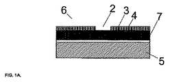
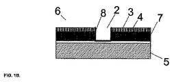
例えば、図1A−1Cに示されるように、従来のリソグラフィ技術を用いて形成されたパターン2を有する感光層3から成るエッチングマスク6は、誘電体層4をエッチングするためのマスクとして使用されることができ、エッチングプロセスにより感光層3内のマスクパターン2が誘電体層4に転写される。下に位置する基板5の層にエッチングプロセスが入り込むことを防止しながらエッチングプロセスを停止させることを容易にするため、エッチング停止層7が用いられ得る。エッチング停止層は、例えば、シリコン処理においては窒化シリコン又は炭化シリコンを含むことができる。エッチングプロセスが行われると、感光性材料の残部とエッチング後の残渣8が造形部9の表面に残される。
For example, as shown in FIGS. 1A-1C, an
エッチングプロセスに続いて、エッチング残渣が除去される。上述のように、従来はこのような残渣を除去するために酸素プラズマが用いられていたが、これら従来プロセスは誘電体層にダメージを与え、多くの場合、この層の誘電率の増大を引き起こすことが観測されている。先端半導体デバイスにおいては、誘電体層は低誘電率(low−k)材料を有している。例えば、誘電体層の誘電率は、およそ4であるSiO2の誘電率(例えば、熱成長された二酸化シリコンの誘電率は3.8から3.9の範囲となり得る)より低い値である。他の例では、誘電率は2.5未満とし得る。例えば、誘電体層は超low−k材料として特徴付けられてもよい。 Following the etching process, etching residues are removed. As noted above, oxygen plasma has traditionally been used to remove such residues, but these conventional processes damage the dielectric layer and often increase the dielectric constant of this layer. It has been observed. In advanced semiconductor devices, the dielectric layer has a low dielectric constant (low-k) material. For example, the dielectric constant of the dielectric layer is lower than the dielectric constant of SiO 2 which is approximately 4 (eg, the dielectric constant of thermally grown silicon dioxide can range from 3.8 to 3.9). In other examples, the dielectric constant may be less than 2.5. For example, the dielectric layer may be characterized as an ultra low-k material.
誘電体層は有機、無機、及び無機−有機ハイブリッド材料のうちの少なくとも1つを含んでいてもよい。また、誘電体層は多孔質であってもよいし、あるいは非多孔質であってもよい。例えば、誘電体層は、CVD技術を用いて堆積された例えば酸化オルガノシラン(又はオルガノシロキサン)等の無機のケイ酸塩ベース材料を含んでいてもよい。このような層の例には、アプライドマテリアル社から商業的に入手可能なBlack Diamond(登録商標)CVD有機ケイ酸塩ガラス(OSG)膜、又はノベラスシステムズ社から商業的に入手可能なCoral(登録商標)CVD膜がある。また、多孔質誘電体層は、例えばキュアプロセス中に破壊されて微小なボイド(又はポア)を作り出すCH3結合を有するシリコン酸化物ベースの充填剤(matrix)などの、単一相材料を含むことができる。また、例えば、多孔質誘電体層は、例えばキュアプロセス中に気化される有機材料(例えば、ポロゲン)のポアを有するシリコン酸化物ベースの充填剤などの、複相材料を含むことができる。他の例では、誘電体層は、SOD技術を用いて堆積された例えば水素シルセスキオキサン(HSQ)又はメチルシルセスキオキサン(MSQ)等の無機のケイ酸塩ベース材料を含んでいてもよい。このような膜の例には、ダウコーニング社から商業的に入手可能なFOxHSQ及びXLK多孔質HSQ、並びにJSRマイクロエレクトロニクス社から商業的に入手可能なJSR LKD−5109がある。更に他の例では、誘電体層はSOD技術を用いて堆積された有機材料を含むことができる。このような膜の例には、ダウケミカル社から商業的に入手可能なSiLK−I、SiLK−J、SiLK−H、SiLK−D及び多孔質SiLK半導体誘電体樹脂、並びにハネウェル社から商業的に入手可能なFLARE(登録商標)及びナノガラスがある。 The dielectric layer may include at least one of organic, inorganic, and inorganic-organic hybrid materials. The dielectric layer may be porous or non-porous. For example, the dielectric layer may include an inorganic silicate-based material, such as oxidized organosilane (or organosiloxane) deposited using CVD techniques. Examples of such layers include Black Diamond® CVD organosilicate glass (OSG) film commercially available from Applied Materials, or Coral®, commercially available from Novellus Systems. Trademark) CVD film. The porous dielectric layer also includes a single phase material, such as a silicon oxide based matrix with CH 3 bonds that are broken during the curing process to create tiny voids (or pores). be able to. Also, for example, the porous dielectric layer can include a multiphase material, such as a silicon oxide-based filler having a pore of an organic material (eg, porogen) that is vaporized during the curing process. In other examples, the dielectric layer may include an inorganic silicate-based material, such as hydrogen silsesquioxane (HSQ) or methyl silsesquioxane (MSQ), deposited using SOD technology. Good. Examples of such membranes include FOx HSQ and XLK porous HSQ commercially available from Dow Corning, and JSR LKD-5109 commercially available from JSR Microelectronics. In yet another example, the dielectric layer can include an organic material deposited using SOD technology. Examples of such films include SiLK-I, SiLK-J, SiLK-H, SiLK-D and porous SiLK semiconductor dielectric resins commercially available from Dow Chemical Company, and commercially available from Honeywell. There are FLARE® and nanoglass available.
窒素(N)含有ガス、水素(H)含有ガス及び酸素(O)含有ガスを含むプロセスガスを用いて誘電体層からエッチング残渣を除去する一実施形態に係るプロセスを説明する。他の例では、窒素(N)、水素(H)及び酸素(O)のうちの2つ以上が単一のガスに含められてもよい。例えば、low−k誘電体層からエッチング残渣を除去する方法として、アンモニア−酸素(NH3/O2)ベースの化学反応が導入されることができる。代替的な一実施形態においては、low−k誘電体層からエッチング残渣を除去するために、窒素−水素−酸素(N2/H2/O2)ベースの化学反応が用いられることができる。他の例では、上述の2つの化学反応におけるO2を置換するために、一酸化炭素(CO)が付加あるいは利用される。他の例では、上述の3つの化学反応におけるO2を置換するために、二酸化炭素(CO2)が付加あるいは利用される。他の例では、プロセスガスは更に、例えば希ガス(すなわち、ヘリウム、ネオン、アルゴン、クリプトン、キセノン等)などの不活性ガスを含むことができる。 A process according to an embodiment of removing an etching residue from a dielectric layer using a process gas including a nitrogen (N) -containing gas, a hydrogen (H) -containing gas, and an oxygen (O) -containing gas will be described. In other examples, two or more of nitrogen (N), hydrogen (H), and oxygen (O) may be included in a single gas. For example, an ammonia-oxygen (NH 3 / O 2 ) based chemical reaction can be introduced as a method of removing etch residues from a low-k dielectric layer. In an alternate embodiment, in order to remove the etching residue from low-k dielectric layer, a nitrogen - hydrogen - oxygen (N 2 / H 2 / O 2) may be based chemistry is used. In another example, carbon monoxide (CO) is added or utilized to replace O 2 in the two chemical reactions described above. In another example, carbon dioxide (CO 2 ) is added or used to replace O 2 in the three chemical reactions described above. In other examples, the process gas can further include an inert gas such as, for example, a noble gas (ie, helium, neon, argon, krypton, xenon, etc.).
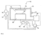
一実施形態に従ったプラズマ処理システム1が図2に示されており、これはプラズマ処理チャンバー10、プラズマ処理チャンバー10に結合された診断系12、及び診断系12とプラズマ処理チャンバー10とに結合されたコントローラ14を有している。コントローラ14は、エッチング後のエッチング残渣を誘電体層から除去するために、上記にて特定された化学反応(すなわち、NH3/O2、N2/H2/O2、NH3/CO、N2/H2/CO、NH3/CO2、N2/H2/CO2等)の少なくとも1つを有するプロセスレシピを実行するように構成されている。また、コントローラ14は、診断系12から少なくとも1つの終点信号を受信し、プロセスの終点を正確に決定するために該少なくとも1つの終点信号を後処理するように構成されている。例示された実施形態においては、図2に示されたプラズマ処理システム1は材料の処理のためにプラズマを使用する。プラズマ処理システム1はエッチングチャンバーを有することができる。
A
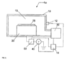
図3に示された一実施形態によれば、プラズマ処理システム1aはプラズマ処理チャンバー10、処理されるべき基板25が上に添えられる基板ホルダー20、及び真空ポンプ系30を有している。基板25は、例えば、半導体基板、ウェハ又は液晶ディスプレーであり得る。プラズマ処理チャンバー10は、基板25の表面に隣接する処理領域15にプラズマを生成することを促進するように構成され得る。イオン化ガス又は混合ガスがガス注入系(図示せず)を介して導入されるとともに、処理圧力が調整される。例えば、真空ポンプ系30を絞るために制御機構(図示せず)が使用される。プラズマは、所定の材料プロセスに特有の材料を作り出し、且つ/或いは基板25の露出面から材料を除去することを助けるために利用され得る。プラズマ処理システム1aは、例えば200mm基板、300mm基板又は更に大きい基板など、任意の大きさの基板を処理するように構成され得る。
According to one embodiment shown in FIG. 3, the
基板25は静電クランプ系によって基板ホルダー20に貼り付けられることができる。また、基板ホルダー20は更に、再循環冷却材流を含む冷却系を含むことができ、この冷却材流は基板ホルダー20から熱を受け取って熱交換器系(図示せず)まで熱伝達し、あるいは加熱時に熱交換器系から熱を伝達する。さらに、基板25と基板ホルダー20との間のガスギャップの熱伝導率を改善するために、基板25の裏面側にガスが供給されてもよい。このようなシステムは、上昇温度又は下降温度での基板の温度制御が要求されるときに利用され得る。例えば、裏面側のガス系は、基板25の中心部と端部との間でガスギャップ圧力を独立に変化させられ得る2区画のガス分配系を有していてもよい。他の実施形態において、例えば抵抗加熱素子又は熱電加熱器/冷却器などの加熱/冷却素子が、基板ホルダー20、プラズマ処理チャンバー10のチャンバー壁、及びプラズマ処理システム1a内のその他の部品に含められ得る。
The
図3に示された実施形態においては、基板ホルダー20は、処理空間15の処理プラズマに無線周波数(RF)電力を結合させる電極を有している。例えば、基板ホルダー20は、RF発生器40から該基板ホルダー20へのインピーダンス整合回路50を介したRF電力の伝送によって、あるRF電圧に電気的にバイアスされることができる。このRFバイアスは電子を加熱し、それによってプラズマを形成・維持するように作用する。この構成において、システムは反応性イオンエッチング(RIE)炉として動作し、チャンバー及び上側のガス供給電極は接地面として作用する。RFバイアスの典型的な周波数は約0.1MHzから約100MHzの範囲とし得る。プラズマ処理のためのRF系は当業者に周知である。
In the embodiment shown in FIG. 3, the
他の例では、RF電力は基板ホルダー電極に複数の周波数で印加される。さらに、インピーダンス整合回路50は、反射される電力を低減することによって、プラズマ処理チャンバー10内のプラズマへのRF電力の移送を改善するように作用する。整合回路トポロジー(例えば、L型、π型、T型など)及び自動制御方法は当業者に周知である。
In other examples, RF power is applied to the substrate holder electrode at multiple frequencies. Furthermore, the
真空ポンプ系30は、例えば、毎秒5000リットルの(及び、これより大きい)速度でポンプ可能なターボ分子真空ポンプ(TMP)と、チャンバー圧力を絞るための仕切り弁とを含み得る。ドライプラズマエッチングで使用される従来からのプラズマ処理装置においては、一般的に、毎秒1000から3000リットルのTMPが使用される。TMPは低圧処理、典型的には約50mTorr未満で有用である。高圧処理(すなわち、約100mTorrより高い)の場合には、機械的な増圧ポンプ及びドライ式の粗引きポンプが使用され得る。また、チャンバー圧力を監視する装置(図示せず)がプラズマ処理チャンバー10に結合されることができる。この圧力測定装置は、例えば、MKSインスツルメント社から市販されている628B型バラトロン(Baratron)絶対キャパシタンス式圧力計とし得る。
The
コントローラ14はマイクロプロセッサ、メモリ、及び、プラズマ処理システム1aからの出力を監視するとともにプラズマ処理システム1aへの入力を伝達し且つアクティブにするに十分な制御電圧を生成可能なデジタルI/Oポートを含んでいる。さらに、コントローラ14は、RF発生器40、インピーダンス整合回路50、ガス注入系(図示せず)、真空ポンプ系30、裏面側ガス注入系(図示せず)、基板/基板ホルダー温度測定系(図示せず)、及び/又は静電クランプ系(図示せず)に結合され、それらと情報を交換することが可能である。例えば、有機ARC層をエッチングする方法を実行するため、プロセスレシピに従ってプラズマ処理システム1aの上述の構成要素への入力をアクティブにするように、メモリ内に格納されたプログラムが使用され得る。コントローラ14の一例は、デル社から入手可能なDELL PRECISION WORKSTATION610(登録商標)である。
The
コントローラ14は、プラズマ処理システム1aに対してローカルに配置されていてもよいし、インターネット又はイントラネットを介してプラズマ処理システム1aに対して遠隔に配置されていてもよい。故に、コントローラ14は、直接接続、イントラネット若しくはインターネット、又はこれらの何らかの組み合わせ、の何れかを用いてプラズマ処理システム1aとデータを交換することができる。コントローラ14は、顧客側(すなわち、デバイスメーカー等)のイントラネットに結合されていてもよいし、製造供給元(すなわち、装置製造者)のイントラネットに結合されていてもよい。さらに、他のコンピュータ(すなわち、コントローラ、サーバ等)が、直接接続、イントラネット若しくはインターネット、又はこれらの何らかの組み合わせ、の何れかを介してデータ交換するために、コントローラ14にアクセスしてもよい。
The
診断系12は光学式診断サブシステム(図示せず)を含み得る。光学式診断サブシステムは、プラズマから放射された光強度を測定する例えば(シリコン)フォトダイオードや光電管(PMT)等の検出器を有している。診断系12は更に、例えば狭帯域干渉フィルタ等の光学フィルタを含み得る。代替的な一実施形態においては、診断系12は、ラインCCD(電荷結合素子)、CID(電荷注入素子)アレイ、若しくは回折格子やプリズム等の光分散素子、又はこれらの何らかの組み合わせを含んでいてもよい。また、診断系12は所与の波長の光を測定する単色分光器(例えば、回折格子/検出器システム)、又は例えば米国特許第5888337号明細書に記載されている装置のような、光のスペクトルを測定する分光計(例えば、回転式回折格子)を含んでいてもよい。
The
診断系12は、例えばピークセンサーシステムズ社又はベリティインスツルメンツ社からのものなど、高分解能の発光分光(OES)センサーを含むことができる。このようなOESセンサーは、紫外(UV)、可視(VIS)及び近赤外(NIR)の光スペクトルに及ぶ広い帯域を有している。分解能はおよそ1.4Åであり、240nmから1000nmまでで5550波長を収集することが可能である。例えば、OESセンサーには高感度の小型光ファイバー式UV−VIS−NIR分光計が備えられ、この分光計は2048画素のリニアCCDアレイに一体化される。
The
分光計は単一あるいは束状の光ファイバーを介して伝送された光を受信し、光ファイバーから出力された光が固定式の回折格子を用いてラインCCDアレイ上に散らされる。上述の構成を用い、光学的な真空窓を通して伝送された光は凸面球状レンズを介して光ファイバーの入力端に集められる。そして、各々が所与のスペクトル範囲(UV、VIS及びNIR)に明確に同調された3つの分光計が処理チャンバー10用のセンサーを形成する。各分光計は独立したA/D変換器を含んでいる。そして最終的に、センサーの使用に応じて、完全な放射スペクトルが0.1秒から1.0秒ごとに記録される。
The spectrometer receives light transmitted through a single or bundled optical fiber, and the light output from the optical fiber is scattered on the line CCD array using a fixed diffraction grating. Using the configuration described above, the light transmitted through the optical vacuum window is collected at the input end of the optical fiber via a convex spherical lens. And three spectrometers, each clearly tuned to a given spectral range (UV, VIS and NIR) form a sensor for the
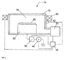
図4に示された一実施形態において、プラズマ処理システム1bは、図2又は3の実施形態と同様であるが、図2及び3を参照して説明された構成要素に加えて更に、プラズマ密度を潜在的に高め、且つ/或いはプラズマ処理の均一性を向上させるために、静止しているか、機械的又は電気的に回転しているかの何れかである磁場系60を有している。また、回転速度及び磁場強度を調整するために磁場系60にコントローラ14が結合されている。回転磁場の設計及び実装は当業者に周知である。
In one embodiment shown in FIG. 4, the
図5に示された一実施形態において、プラズマ処理システム1cは、図2又は3の実施形態と同様であるが、更に、RF発生器72からインピーダンス整合回路74を介してRF電力が結合され得る上部電極70を有している。この上部電極へのRF電力印加の典型的な周波数は約0.1MHzから約200MHzの範囲とし得る。さらに、下部電極への電力印加の典型的な周波数は約0.1MHzから約100MHzの範囲とし得る。また、上部電極70へのRF電力の印加を制御するため、RF発生器72及びインピーダンス整合回路74にコントローラ14が結合されている。上部電極の設計及び実装は当業者に周知である。
In one embodiment shown in FIG. 5, the plasma processing system 1c is similar to the embodiment of FIG. 2 or 3, but further RF power can be coupled from the
図6に示された一実施形態において、プラズマ処理システム1dは、図2及び3の実施形態と同様であるが、更に、RF発生器82からインピーダンス整合回路84を介してRF電力が結合される誘導コイル80を有している。RF電力は誘導コイル80から誘電体窓(図示せず)を介してプラズマ処理領域15に誘導的に結合される。誘導コイル80へのRF電力印加の典型的な周波数は約10MHzから約100MHzの範囲とし得る。同様に、チャック電極への電力印加の典型的な周波数は約0.1MHzから約100MHzの範囲とし得る。さらに、誘導コイル80とプラズマとの間の容量結合を低減させるために、スロット式ファラデー遮蔽体(図示せず)が用いられ得る。また、誘導コイル80への電力印加を制御するため、RF発生器82及びインピーダンス整合回路84にコントローラ14が結合されている。代替的な一実施形態においては、誘導コイル80はトランス結合型プラズマ(TCP)炉においてのように上方からプラズマ処理領域15に作用する“螺旋状”コイル又は“パンケーキ型”コイルとし得る。誘導結合型プラズマ(ICP)源又はトランス結合型プラズマ(TCP)源の設計及び実装は当業者に周知である。
In one embodiment shown in FIG. 6, the plasma processing system 1d is similar to the embodiment of FIGS. 2 and 3, but further RF power is coupled from the
他の例では、プラズマは電子サイクロトロン共鳴(ECR)によって形成されてもよい。更に他の一実施形態においては、プラズマはヘリコン波の放射によって形成される。更に他の一実施形態においては、プラズマは伝播表面波によって形成される。これらの各プラズマ源は当業者に周知である。 In other examples, the plasma may be formed by electron cyclotron resonance (ECR). In yet another embodiment, the plasma is formed by helicon wave radiation. In yet another embodiment, the plasma is formed by propagating surface waves. Each of these plasma sources is well known to those skilled in the art.
以上の説明にて、プラズマ処理を用いて誘電体層からエッチング残渣を除去する方法が提示された。プラズマ処理装置は、例えば図2乃至6に関して説明された要素又はこれらの組み合わせ等の様々な要素を有し得る。 In the above description, a method for removing etching residues from a dielectric layer using plasma treatment has been presented. The plasma processing apparatus may have various elements such as, for example, the elements described with respect to FIGS.
一実施形態において、誘電体層からエッチング残渣を除去する方法はNH3/COベースの化学反応を含む。例えば、プロセスパラメータ空間は、約10mTorrから約1000mTorrのチャンバー圧力、約50sccmから約2000sccmの範囲のNH3プロセスガス流量、約50sccmから約1000sccmの範囲のCOプロセスガス流量、約0Wから約2000Wの範囲の上部電極(例えば、図5の要素70)のRFバイアス、及び約10Wから約1000Wの範囲の下部電極(例えば、図5の要素20)のRFバイアスを有し得る。また、上部電極のバイアス周波数は約0.1MHzから約200MHzの範囲とすることができ、例えば約60MHzである。さらに、下部電極のバイアス周波数は約0.1MHzから約100MHzの範囲とすることができ、例えば約2MHzである。
In one embodiment, the method of removing etch residues from the dielectric layer includes a NH 3 / CO based chemical reaction. For example, the process parameter space may be a chamber pressure of about 10 mTorr to about 1000 mTorr, an NH 3 process gas flow rate in the range of about 50 sccm to about 2000 sccm, a CO process gas flow rate in the range of about 50 sccm to about 1000 sccm, a range of about 0 W to about 2000 W. The RF bias of the upper electrode (eg,
他の一実施形態において、誘電体層からエッチング残渣を除去する方法はNH3/O2ベースの化学反応を含む。例えば、プロセスパラメータ空間は、約20mTorrから約1000mTorrのチャンバー圧力、約50sccmから約2000sccmの範囲のNH3プロセスガス流量、約50sccmから約1000sccmの範囲のO2プロセスガス流量、約0Wから約2000Wの範囲の上部電極(例えば、図5の要素70)のRFバイアス、及び約10Wから約1000Wの範囲の下部電極(例えば、図5の要素20)のRFバイアスを有し得る。また、上部電極のバイアス周波数は約0.1MHzから約200MHzの範囲とすることができ、例えば約60MHzである。さらに、下部電極のバイアス周波数は約0.1MHzから約100MHzの範囲とすることができ、例えば約2MHzである。
In another embodiment, the method of removing etch residues from the dielectric layer includes a NH 3 / O 2 based chemical reaction. For example, the process parameter space can be a chamber pressure of about 20 mTorr to about 1000 mTorr, an NH 3 process gas flow rate in the range of about 50 sccm to about 2000 sccm, an O 2 process gas flow rate in the range of about 50 sccm to about 1000 sccm, about 0 W to about 2000 W. The RF bias of the upper electrode (eg,
更に他の一実施形態において、誘電体層からエッチング残渣を除去する方法はNH3/CO2ベースの化学反応を含む。例えば、プロセスパラメータ空間は、約20mTorrから約1000mTorrのチャンバー圧力、約50sccmから約2000sccmの範囲のNH3プロセスガス流量、約50sccmから約1000sccmの範囲のCO2プロセスガス流量、約0Wから約2000Wの範囲の上部電極(例えば、図5の要素70)のRFバイアス、及び約10Wから約1000Wの範囲の下部電極(例えば、図5の要素20)のRFバイアスを有し得る。また、上部電極のバイアス周波数は約0.1MHzから約200MHzの範囲とすることができ、例えば約60MHzである。さらに、下部電極のバイアス周波数は約0.1MHzから約100MHzの範囲とすることができ、例えば約2MHzである。
In yet another embodiment, a method for removing etch residues from a dielectric layer includes a NH 3 / CO 2 based chemical reaction. For example, the process parameter space may be a chamber pressure of about 20 mTorr to about 1000 mTorr, an NH 3 process gas flow rate in the range of about 50 sccm to about 2000 sccm, a CO 2 process gas flow rate in the range of about 50 sccm to about 1000 sccm, about 0 W to about 2000 W. The RF bias of the upper electrode (eg,
一実施例として、例えば図5にて説明された装置などのプラズマ処理装置を用いて誘電体層からエッチング残渣を除去する方法が提示される。しかしながら、ここで説明される方法の範囲はこの例示的な提示によって限定されるものではない。表1は、以下の典型的なプロセスレシピを用いたときの、(SiCOH low−k)誘電体層内にエッチングされた造形部のエッチング残渣の除去後の限界寸法(critical dimension;CD)(頂部、中央部、及び底部)(nm)と、エッチング残渣除去の前後での造形部の限界寸法の変化(CDシフト)(nm)とを示している:チャンバー圧力=約400mTorr;上部電極RF電力=約0W;下部電極RF電力=約300W;プロセスガス流量NH3/CO=約1200/600sccm;電極70(図5参照)の下側表面と基板ホルダー20上の基板25の上側表面との間の間隔=約60mm;下部電極(例えば、図5の基板ホルダー20)温度=約20℃;上部電極(例えば、図5の電極70)温度=約60℃;チャンバー壁温度=約60℃;中心部/端部での裏面側ヘリウム圧力=約10/35Torr;及びエッチング時間=約125s。限界寸法及びその変化は、ネスト化された造形部(空間的に密接した造形部)及び離隔化された造形部(空間的に広く離隔された造形部)に関して提示されている。
As an example, a method for removing etching residues from a dielectric layer using a plasma processing apparatus such as the apparatus described in FIG. 5 is presented. However, the scope of the method described herein is not limited by this exemplary presentation. Table 1 shows the critical dimension (CD) (top) after removal of etch residues of features etched in a (SiCOH low-k) dielectric layer using the following typical process recipe: , Center and bottom) (nm) and change in critical dimension (CD shift) (nm) of the shaped part before and after etching residue removal: chamber pressure = about 400 mTorr; top electrode RF power = About 0 W; lower electrode RF power = about 300 W; process gas flow rate NH 3 / CO = about 1200/600 sccm; between the lower surface of the electrode 70 (see FIG. 5) and the upper surface of the
また、限界寸法及びその変化は、誘電体層からエッチング残渣を除去するためのその他2つのプロセスレシピに関しても提示されている。第1に、従来の酸素(O2)ベースの化学反応が提示されている:チャンバー圧力=約20mTorr;上部電極RF電力=約300W;下部電極RF電力=約0W;プロセスガス流量O2/Ar=約200/550sccm;電極70(図5参照)の下側表面と基板ホルダー20上の基板25の上側表面との間の間隔=約60mm;下部電極(例えば、図5の基板ホルダー20)温度=約20℃;上部電極(例えば、図5の電極70)温度=約60℃;チャンバー壁温度=約60℃;中心部/端部での裏面側ヘリウム圧力=約10/35Torr;及びエッチング時間=約55s。第2に、アンモニア(NH3)ベースの化学反応が提示されている:チャンバー圧力=約400mTorr;上部電極RF電力=約0W;下部電極RF電力=約300W;プロセスガス流量NH3=約1800sccm;電極70(図5参照)の下側表面と基板ホルダー20上の基板25の上側表面との間の間隔=約60mm;下部電極(例えば、図5の基板ホルダー20)温度=約20℃;上部電極(例えば、図5の電極70)温度=約60℃;チャンバー壁温度=約60℃;中心部/端部での裏面側ヘリウム圧力=約10/35Torr;及びエッチング時間=約120s。
Critical dimensions and their variations are also presented for two other process recipes for removing etch residues from dielectric layers. First, a conventional oxygen (O 2 ) based chemical reaction is presented: chamber pressure = about 20 mTorr; upper electrode RF power = about 300 W; lower electrode RF power = about 0 W; process gas flow rate O 2 / Ar = About 200/550 sccm; spacing between the lower surface of electrode 70 (see FIG. 5) and the upper surface of

図7は、プラズマ処理システム内で基板上の(low−k)誘電体層からエッチング残渣を除去するための、本発明の一実施形態に従った方法を示すフローチャートである。手順400は段階410にて開始され、窒素(N)含有ガス、水素(H)含有ガス及び酸素(O)含有ガスを含むプロセスガスが、プラズマ処理システムに導入される。例えば、プロセスガスはアンモニア(NH3)及び二原子酸素(O2)を含むことができる。他の例では、プロセスガスは二原子窒素(N2)、二原子水素(H2)及び二原子酸素(O2)を含むことができる。他の例では、プロセスガスはアンモニア(NH3)及び一酸化炭素(CO)を含むことができる。他の例では、プロセスガスは二原子窒素(N2)、二原子水素(H2)及び一酸化炭素(CO)を含むことができる。他の例では、プロセスガスはアンモニア(NH3)及び二酸化炭素(CO2)を含むことができる。他の例では、プロセスガスは二原子窒素(N2)、二原子水素(H2)及び二酸化炭素(CO2)を含むことができる。他の例では、プロセスガスは更に、例えば希ガス等の不活性ガスを含むことができる。
FIG. 7 is a flowchart illustrating a method according to one embodiment of the present invention for removing etch residues from a (low-k) dielectric layer on a substrate in a plasma processing system. The
段階420にて、例えば、図2乃至6にて説明されたシステムの何れか又はそれらの組み合わせを用いて、プラズマ処理システム内でプロセスガスからプラズマが形成される。
At
段階430にて、エッチング残渣を上に有する誘電体層を備えた基板が段階420で形成されたプラズマに晒され、誘電体層にダメージを与えることなくエッチング残渣が除去される。この実施形態において、このプラズマに晒す段階は、誘電体層の下に位置するエッチング停止層の厚さを低減させ得るが、それはおよそ10%未満である。
In
以上では本発明の特定の実施形態のみが詳細に説明されているが、当業者に容易に認識されるように、これらの実施形態には、本発明の新規な教示及び効果を実質的に逸脱することなく数多くの変更が為され得る。従って、全てのそのような変更は本発明の範囲に含まれるものである。 Although only specific embodiments of the present invention have been described in detail above, as those skilled in the art will readily appreciate, these embodiments substantially depart from the novel teachings and advantages of the present invention. Many changes can be made without doing so. Accordingly, all such modifications are intended to be included within the scope of this invention.
Claims (22)
誘電体層を有する前記基板をプラズマ処理システム内に配置する段階であり、該誘電体層は、その内部に、エッチングプロセスを用いて形成された造形部を有し、且つ該造形部は、その上に、前記エッチングプロセスによって形成された前記エッチング残渣を有する、段階;
窒素含有ガス、水素含有ガス及び酸素含有ガスを含むプロセスガスを導入する段階であり、該酸素含有ガスは、O2、CO、若しくはCO2、又はこれらの組み合わせを含む、段階;
前記プラズマ処理システム内で前記プロセスガスからプラズマを形成する段階;及び
前記エッチング残渣を除去するために前記プラズマに前記基板を晒す段階;
を有し、
前記誘電体層はSiO2の誘電率より低い誘電率を有する、方法。 A method for removing etching residues from a substrate comprising:
Disposing the substrate having a dielectric layer in a plasma processing system, the dielectric layer having a shaped portion formed therein using an etching process, and the shaped portion comprising: Having the etching residue formed by the etching process on the top;
Introducing a process gas comprising a nitrogen-containing gas, a hydrogen-containing gas and an oxygen-containing gas, the oxygen-containing gas comprising O 2 , CO, or CO 2 , or combinations thereof;
Forming a plasma from the process gas in the plasma processing system; and exposing the substrate to the plasma to remove the etching residue;
Have
The method, wherein the dielectric layer has a dielectric constant lower than that of SiO 2 .
誘電体層を有する前記基板をプラズマ処理システム内に配置する段階であり、該誘電体層は、その内部に、エッチングプロセスを用いて形成された造形部を有し、該造形部は、その上に、前記エッチングプロセスによって形成された前記エッチング残渣を有し、且つ前記誘電体層はSiO2の誘電率より低い誘電率を有する、段階;
窒素含有ガス、水素含有ガス及び酸素含有ガスを含むプロセスガスを導入する段階であり、該酸素含有ガスは、CO、若しくはCO2、又はこれら双方を含む、段階;
前記プラズマ処理システム内で前記プロセスガスからプラズマを形成する段階;及び
前記誘電体層の誘電率に実質的な変化を生じさせずに前記エッチング残渣を除去するために前記プラズマに前記基板を晒す段階;
を有する方法。 A method for removing etching residues from a substrate comprising:
Disposing the substrate having a dielectric layer in a plasma processing system, the dielectric layer having a shaped part formed therein using an etching process, the shaped part being formed thereon; And having the etching residue formed by the etching process and the dielectric layer having a dielectric constant lower than that of SiO 2 ;
Introducing a process gas comprising a nitrogen-containing gas, a hydrogen-containing gas and an oxygen-containing gas, wherein the oxygen-containing gas comprises CO, CO 2 , or both;
Forming a plasma from the process gas in the plasma processing system; and exposing the substrate to the plasma to remove the etching residue without causing a substantial change in the dielectric constant of the dielectric layer. ;
Having a method.
前記造形部から前記エッチング残渣を除去するために、プロセスガスからのプラズマの形成を促進させるプラズマ処理チャンバー;及び
前記プラズマ処理チャンバーに結合され、且つ前記プロセスガスを用いてプロセスレシピを実行するように構成されたコントローラであり、前記プロセスガスは窒素含有ガス、水素含有ガス及び酸素含有ガスを含み、該酸素含有ガスは、O2、CO、若しくはCO2、又はこれらの組み合わせを含み、前記誘電体層はSiO2の誘電率より低い誘電率を有し、且つ前記エッチング残渣の除去は前記誘電体層の誘電率に実質的な変化を生じさせない、コントローラ;
を有するプラズマ処理システム。 A plasma processing system for removing etching residues from a shaped part in a dielectric layer on a substrate comprising:
A plasma processing chamber for promoting the formation of plasma from a process gas to remove the etching residue from the shaped part; and a process recipe coupled to the plasma processing chamber and using the process gas A controller configured, wherein the process gas includes a nitrogen-containing gas, a hydrogen-containing gas, and an oxygen-containing gas, the oxygen-containing gas including O 2 , CO, or CO 2 , or a combination thereof, and the dielectric A controller having a dielectric constant lower than that of SiO 2 and removal of the etching residue does not cause a substantial change in the dielectric constant of the dielectric layer;
A plasma processing system.
前記造形部から前記エッチング残渣を除去するために、プロセスガスからのプラズマの形成を促進させるプラズマ処理チャンバー;及び
前記プラズマ処理チャンバーに結合され、且つ前記プロセスガスを用いてプロセスレシピを実行するように構成されたコントローラであり、前記プロセスガスは窒素含有ガス、水素含有ガス及び酸素含有ガスを含み、該酸素含有ガスは、CO、若しくはCO2、又はこれら双方を含み、前記誘電体層はSiO2の誘電率より低い誘電率を有し、且つ前記エッチング残渣の除去は前記誘電体層の誘電率に実質的な変化を生じさせない、コントローラ;
を有するプラズマ処理システム。 A plasma processing system for removing etching residues from a shaped part in a dielectric layer on a substrate comprising:
A plasma processing chamber for promoting the formation of plasma from a process gas to remove the etching residue from the shaped part; and a process recipe coupled to the plasma processing chamber and using the process gas The process gas includes a nitrogen-containing gas, a hydrogen-containing gas, and an oxygen-containing gas, and the oxygen-containing gas includes CO, CO 2 , or both, and the dielectric layer includes SiO 2. A controller having a lower dielectric constant than the dielectric constant and removal of the etching residue does not cause a substantial change in the dielectric constant of the dielectric layer;
A plasma processing system.
誘電体層を有する基板を前記プラズマ処理システム内に配置する段階であり、該誘電体層は、その内部に、エッチングプロセスを用いて形成された造形部を有し、該造形部は、その上に、前記エッチングプロセスによって形成されたエッチング残渣を有し、且つ該誘電体層はSiO2の誘電率より低い誘電率を有する、段階;
窒素含有ガス、水素含有ガス及び酸素含有ガスを含むプロセスガスを導入する段階であり、該酸素含有ガスは、O2、CO、若しくはCO2、又はこれらの組み合わせを含む、段階;
前記プラズマ処理システム内で前記プロセスガスからプラズマを形成する段階;及び
前記エッチング残渣を除去するために前記プラズマに前記基板を晒す段階;
を実行させる、コンピュータ読み取り可能媒体。 A computer readable medium having stored thereon program instructions executed on a computer system, the program instructions causing the computer system to control a plasma processing system when executed on the computer system:
A step of disposing a substrate having a dielectric layer in the plasma processing system, the dielectric layer having a modeling portion formed therein by using an etching process, And having an etching residue formed by the etching process, and the dielectric layer has a dielectric constant lower than that of SiO 2 ;
Introducing a process gas comprising a nitrogen-containing gas, a hydrogen-containing gas and an oxygen-containing gas, the oxygen-containing gas comprising O 2 , CO, or CO 2 , or combinations thereof;
Forming a plasma from the process gas in the plasma processing system; and exposing the substrate to the plasma to remove the etching residue;
A computer-readable medium for executing
Applications Claiming Priority (2)
| Application Number | Priority Date | Filing Date | Title |
|---|---|---|---|
| US11/195,854 US7279427B2 (en) | 2005-08-03 | 2005-08-03 | Damage-free ashing process and system for post low-k etch |
| PCT/US2006/019914 WO2007018678A2 (en) | 2005-08-03 | 2006-05-24 | Damage-free ashing process and system for post low-k etch |
Publications (2)
| Publication Number | Publication Date |
|---|---|
| JP2009503889A true JP2009503889A (en) | 2009-01-29 |
| JP2009503889A5 JP2009503889A5 (en) | 2009-03-26 |
Family
ID=37718178
Family Applications (1)
| Application Number | Title | Priority Date | Filing Date |
|---|---|---|---|
| JP2008524962A Pending JP2009503889A (en) | 2005-08-03 | 2006-05-24 | Damage-free ashing process and system after low dielectric constant film etching |
Country Status (6)
| Country | Link |
|---|---|
| US (1) | US7279427B2 (en) |
| JP (1) | JP2009503889A (en) |
| KR (1) | KR20080034001A (en) |
| CN (1) | CN100595891C (en) |
| TW (1) | TWI336107B (en) |
| WO (1) | WO2007018678A2 (en) |
Cited By (3)
| Publication number | Priority date | Publication date | Assignee | Title |
|---|---|---|---|---|
| JP2013528928A (en) * | 2010-03-29 | 2013-07-11 | 東京エレクトロン株式会社 | Method for integrating low dielectric constant insulators |
| JP2015523734A (en) * | 2012-07-10 | 2015-08-13 | アプライド マテリアルズ インコーポレイテッドApplied Materials,Incorporated | Method for patterning a low-k dielectric film |
| JP2020125223A (en) * | 2019-02-04 | 2020-08-20 | 国立大学法人東海国立大学機構 | Producing method of carbon nitride film and producing method of carbon nitride coated body |
Families Citing this family (25)
| Publication number | Priority date | Publication date | Assignee | Title |
|---|---|---|---|---|
| JP5100057B2 (en) * | 2006-08-18 | 2012-12-19 | 東京エレクトロン株式会社 | Manufacturing method of semiconductor device |
| US7595005B2 (en) * | 2006-12-11 | 2009-09-29 | Tokyo Electron Limited | Method and apparatus for ashing a substrate using carbon dioxide |
| CN101762993B (en) * | 2008-12-25 | 2012-01-25 | 中芯国际集成电路制造(上海)有限公司 | Method for removing photoresist and method for manufacturing connecting hole |
| CN101930179B (en) * | 2009-06-19 | 2012-08-22 | 中芯国际集成电路制造(上海)有限公司 | Method for passivating photoresist surface and photoetching method |
| US7637269B1 (en) * | 2009-07-29 | 2009-12-29 | Tokyo Electron Limited | Low damage method for ashing a substrate using CO2/CO-based process |
| CN102142393B (en) * | 2010-01-28 | 2013-07-03 | 中芯国际集成电路制造(上海)有限公司 | Forming method of interconnection structure |
| US9338871B2 (en) | 2010-01-29 | 2016-05-10 | Applied Materials, Inc. | Feedforward temperature control for plasma processing apparatus |
| US8916793B2 (en) | 2010-06-08 | 2014-12-23 | Applied Materials, Inc. | Temperature control in plasma processing apparatus using pulsed heat transfer fluid flow |
| US8741775B2 (en) * | 2011-07-20 | 2014-06-03 | Applied Materials, Inc. | Method of patterning a low-K dielectric film |
| US10274270B2 (en) | 2011-10-27 | 2019-04-30 | Applied Materials, Inc. | Dual zone common catch heat exchanger/chiller |
| CN103187360B (en) * | 2011-12-30 | 2016-01-06 | 中芯国际集成电路制造(上海)有限公司 | Form the method for interconnection structure |
| US8592327B2 (en) * | 2012-03-07 | 2013-11-26 | Tokyo Electron Limited | Formation of SiOCl-containing layer on exposed low-k surfaces to reduce low-k damage |
| CN103545163B (en) * | 2012-07-10 | 2016-11-16 | 中芯国际集成电路制造(上海)有限公司 | There is the processing method of the semiconductor structure of fluorine residue or chlorine residual |
| US9165783B2 (en) | 2012-11-01 | 2015-10-20 | Applied Materials, Inc. | Method of patterning a low-k dielectric film |
| CN103871961B (en) | 2012-12-17 | 2017-08-25 | 中芯国际集成电路制造(上海)有限公司 | Interconnection structure and its manufacture method |
| CN103871959B (en) | 2012-12-17 | 2017-11-03 | 中芯国际集成电路制造(上海)有限公司 | Interconnection structure and its manufacture method |
| CN103871962B (en) | 2012-12-18 | 2017-12-29 | 中芯国际集成电路制造(上海)有限公司 | Interconnection structure and its manufacture method |
| FR3000602B1 (en) * | 2012-12-28 | 2016-06-24 | Commissariat A L Energie Atomique Et Aux Energies Alternatives | METHOD FOR ETCHING A POROUS DIELECTRIC MATERIAL |
| US9190317B2 (en) | 2013-01-10 | 2015-11-17 | Semiconductor Manufacturing International (Shanghai) Corporation | Interconnection structures and fabrication method thereof |
| US8987139B2 (en) * | 2013-01-29 | 2015-03-24 | Applied Materials, Inc. | Method of patterning a low-k dielectric film |
| US9385000B2 (en) | 2014-01-24 | 2016-07-05 | United Microelectronics Corp. | Method of performing etching process |
| CN103943555B (en) * | 2014-04-28 | 2016-11-02 | 上海华力微电子有限公司 | A kind of active area preparation method |
| US10312075B2 (en) * | 2015-09-30 | 2019-06-04 | Taiwan Semiconductor Manufacturing Company, Ltd. | Treatment system and method |
| US10199223B2 (en) * | 2016-01-26 | 2019-02-05 | Asm Ip Holding B.V. | Semiconductor device fabrication using etch stop layer |
| CN109742019B (en) * | 2019-01-21 | 2019-10-01 | 广东工业大学 | A method of utilizing hard mask plate in ultraviolet laser processing dry etching |
Citations (3)
| Publication number | Priority date | Publication date | Assignee | Title |
|---|---|---|---|---|
| JP2001077086A (en) * | 1999-08-31 | 2001-03-23 | Oki Electric Ind Co Ltd | Dry etching method of semiconductor device |
| WO2003090267A1 (en) * | 2002-04-16 | 2003-10-30 | Tokyo Electron Limited | Method for removing photoresist and etch residues |
| JP2004158691A (en) * | 2002-11-07 | 2004-06-03 | Yac Co Ltd | Resist removing method |
Family Cites Families (7)
| Publication number | Priority date | Publication date | Assignee | Title |
|---|---|---|---|---|
| JP3193265B2 (en) * | 1995-05-20 | 2001-07-30 | 東京エレクトロン株式会社 | Plasma etching equipment |
| US6967173B2 (en) * | 2000-11-15 | 2005-11-22 | Texas Instruments Incorporated | Hydrogen plasma photoresist strip and polymeric residue cleanup processs for low dielectric constant materials |
| US7833957B2 (en) * | 2002-08-22 | 2010-11-16 | Daikin Industries, Ltd. | Removing solution |
| US7344991B2 (en) * | 2002-12-23 | 2008-03-18 | Tokyo Electron Limited | Method and apparatus for multilayer photoresist dry development |
| AU2003297861A1 (en) * | 2002-12-23 | 2004-07-29 | Tokyo Electron Limited | Method and apparatus for bilayer photoresist dry development |
| US7309448B2 (en) * | 2003-08-08 | 2007-12-18 | Applied Materials, Inc. | Selective etch process of a sacrificial light absorbing material (SLAM) over a dielectric material |
| US7176141B2 (en) * | 2004-09-07 | 2007-02-13 | Taiwan Semiconductor Manufacturing Co., Ltd. | Plasma treatment to improve barrier layer performance over porous low-K insulating dielectrics |
-
2005
- 2005-08-03 US US11/195,854 patent/US7279427B2/en active Active
-
2006
- 2006-05-24 KR KR1020087004579A patent/KR20080034001A/en not_active Application Discontinuation
- 2006-05-24 WO PCT/US2006/019914 patent/WO2007018678A2/en active Application Filing
- 2006-05-24 CN CN200680028670A patent/CN100595891C/en not_active Expired - Fee Related
- 2006-05-24 JP JP2008524962A patent/JP2009503889A/en active Pending
- 2006-08-01 TW TW095128131A patent/TWI336107B/en not_active IP Right Cessation
Patent Citations (4)
| Publication number | Priority date | Publication date | Assignee | Title |
|---|---|---|---|---|
| JP2001077086A (en) * | 1999-08-31 | 2001-03-23 | Oki Electric Ind Co Ltd | Dry etching method of semiconductor device |
| WO2003090267A1 (en) * | 2002-04-16 | 2003-10-30 | Tokyo Electron Limited | Method for removing photoresist and etch residues |
| JP2005523585A (en) * | 2002-04-16 | 2005-08-04 | 東京エレクトロン株式会社 | Method for removing photoresist and etching residue |
| JP2004158691A (en) * | 2002-11-07 | 2004-06-03 | Yac Co Ltd | Resist removing method |
Cited By (4)
| Publication number | Priority date | Publication date | Assignee | Title |
|---|---|---|---|---|
| JP2013528928A (en) * | 2010-03-29 | 2013-07-11 | 東京エレクトロン株式会社 | Method for integrating low dielectric constant insulators |
| JP2015523734A (en) * | 2012-07-10 | 2015-08-13 | アプライド マテリアルズ インコーポレイテッドApplied Materials,Incorporated | Method for patterning a low-k dielectric film |
| JP2020125223A (en) * | 2019-02-04 | 2020-08-20 | 国立大学法人東海国立大学機構 | Producing method of carbon nitride film and producing method of carbon nitride coated body |
| JP7296093B2 (en) | 2019-02-04 | 2023-06-22 | 国立大学法人東海国立大学機構 | Method for producing carbon nitride film and method for producing carbon nitride coating |
Also Published As
| Publication number | Publication date |
|---|---|
| US7279427B2 (en) | 2007-10-09 |
| KR20080034001A (en) | 2008-04-17 |
| TW200721300A (en) | 2007-06-01 |
| CN101238551A (en) | 2008-08-06 |
| CN100595891C (en) | 2010-03-24 |
| US20070032087A1 (en) | 2007-02-08 |
| TWI336107B (en) | 2011-01-11 |
| WO2007018678A2 (en) | 2007-02-15 |
| WO2007018678A3 (en) | 2007-07-12 |
Similar Documents
| Publication | Publication Date | Title |
|---|---|---|
| JP2009503889A (en) | Damage-free ashing process and system after low dielectric constant film etching | |
| US7595005B2 (en) | Method and apparatus for ashing a substrate using carbon dioxide | |
| KR101220073B1 (en) | Method of etching a silicon layer on a substrate, plasma processing system for etching a silicon layer on a substrate and computer readable medium | |
| US7732340B2 (en) | Method for adjusting a critical dimension in a high aspect ratio feature | |
| KR101037308B1 (en) | Method and system for etching a high-k dielectric material | |
| WO2009079284A1 (en) | Method and system for reducing line edge roughness during pattern etching | |
| US7465673B2 (en) | Method and apparatus for bilayer photoresist dry development | |
| KR100989107B1 (en) | Method and apparatus for multilayer photoresist dry development | |
| US20050136681A1 (en) | Method and apparatus for removing photoresist from a substrate | |
| US7344991B2 (en) | Method and apparatus for multilayer photoresist dry development | |
| US20080128388A1 (en) | Method and apparatus for multilayer photoresist dry development | |
| JP2009512998A (en) | Process and system for etching doped silicon | |
| US7767926B2 (en) | Method and system for dry development of a multi-layer mask using sidewall passivation and mask passivation | |
| US20050136666A1 (en) | Method and apparatus for etching an organic layer |
Legal Events
| Date | Code | Title | Description |
|---|---|---|---|
| A521 | Request for written amendment filed |
Free format text: JAPANESE INTERMEDIATE CODE: A523 Effective date: 20090204 |
|
| A621 | Written request for application examination |
Free format text: JAPANESE INTERMEDIATE CODE: A621 Effective date: 20090204 |
|
| A131 | Notification of reasons for refusal |
Free format text: JAPANESE INTERMEDIATE CODE: A131 Effective date: 20110920 |
|
| A521 | Request for written amendment filed |
Free format text: JAPANESE INTERMEDIATE CODE: A523 Effective date: 20111118 |
|
| A131 | Notification of reasons for refusal |
Free format text: JAPANESE INTERMEDIATE CODE: A131 Effective date: 20120515 |
|
| A02 | Decision of refusal |
Free format text: JAPANESE INTERMEDIATE CODE: A02 Effective date: 20121218 |