JP2009503784A - Pressure relief of electrical connector at board interface - Google Patents

Pressure relief of electrical connector at board interface Download PDF

Info

Publication number
JP2009503784A
JP2009503784A JP2008523910A JP2008523910A JP2009503784A JP 2009503784 A JP2009503784 A JP 2009503784A JP 2008523910 A JP2008523910 A JP 2008523910A JP 2008523910 A JP2008523910 A JP 2008523910A JP 2009503784 A JP2009503784 A JP 2009503784A
Authority
JP
Japan
Prior art keywords
wafer
electrical connector
contact
flexible member
lead frame
Prior art date
Legal status (The legal status is an assumption and is not a legal conclusion. Google has not performed a legal analysis and makes no representation as to the accuracy of the status listed.)
Pending
Application number
JP2008523910A
Other languages
Japanese (ja)
Inventor
ミニッチ、スティーブン
Original Assignee
エフシーアイ
Priority date (The priority date is an assumption and is not a legal conclusion. Google has not performed a legal analysis and makes no representation as to the accuracy of the date listed.)
Filing date
Publication date
Application filed by エフシーアイ filed Critical エフシーアイ
Publication of JP2009503784A publication Critical patent/JP2009503784A/en
Pending legal-status Critical Current

Links

Images

Classifications

    • HELECTRICITY
    • H01ELECTRIC ELEMENTS
    • H01RELECTRICALLY-CONDUCTIVE CONNECTIONS; STRUCTURAL ASSOCIATIONS OF A PLURALITY OF MUTUALLY-INSULATED ELECTRICAL CONNECTING ELEMENTS; COUPLING DEVICES; CURRENT COLLECTORS
    • H01R12/00Structural associations of a plurality of mutually-insulated electrical connecting elements, specially adapted for printed circuits, e.g. printed circuit boards [PCB], flat or ribbon cables, or like generally planar structures, e.g. terminal strips, terminal blocks; Coupling devices specially adapted for printed circuits, flat or ribbon cables, or like generally planar structures; Terminals specially adapted for contact with, or insertion into, printed circuits, flat or ribbon cables, or like generally planar structures
    • H01R12/50Fixed connections
    • H01R12/51Fixed connections for rigid printed circuits or like structures
    • H01R12/55Fixed connections for rigid printed circuits or like structures characterised by the terminals
    • H01R12/57Fixed connections for rigid printed circuits or like structures characterised by the terminals surface mounting terminals
    • HELECTRICITY
    • H01ELECTRIC ELEMENTS
    • H01RELECTRICALLY-CONDUCTIVE CONNECTIONS; STRUCTURAL ASSOCIATIONS OF A PLURALITY OF MUTUALLY-INSULATED ELECTRICAL CONNECTING ELEMENTS; COUPLING DEVICES; CURRENT COLLECTORS
    • H01R13/00Details of coupling devices of the kinds covered by groups H01R12/70 or H01R24/00 - H01R33/00
    • H01R13/46Bases; Cases
    • H01R13/50Bases; Cases formed as an integral body
    • H01R13/501Bases; Cases formed as an integral body comprising an integral hinge or a frangible part

Abstract

【解決手段】電気コネクタは、PCB上のハンダパッドの移動に応じてウェーハが膨張するか収縮することを可能にする可撓性部材を有するウェーハを有する。
コネクタが取付けられているPCBは、例えば正常な使用の間に、加熱されて、それは膨張してもよく、PCBとの接続点で、前記ハンダボールの外方への移動に帰着することができる。前記ウェーハにおける可撓性部材は、それが半田接続の移動を妨害せず、PCB接続点のハンダ接続に圧力をかけないように、そのウェーハが同様に膨張することを可能にする。
【選択図】
図7
An electrical connector includes a wafer having a flexible member that allows the wafer to expand or contract in response to movement of a solder pad on the PCB.
The PCB to which the connector is attached is heated, for example during normal use, and it may expand, resulting in outward movement of the solder ball at the point of connection with the PCB. . The flexible member on the wafer allows the wafer to similarly expand so that it does not interfere with the movement of the solder connection and does not put pressure on the solder connection at the PCB connection point.
[Selection]
FIG.

Description

一般に、この発明は、電気コネクタに関する。より特別には、この発明は、基板に接続された接点の相対的移動を可能にするコネクタに関する。   In general, the present invention relates to electrical connectors. More particularly, the present invention relates to a connector that allows relative movement of contacts connected to a substrate.

プリント回路基板(「PCB」)のような基板は、一般に、電子部品を設置し、かつPCBに対してそれらの部品と外部の部品との間の電気的な相互接続を提供するために使用される。コネクタの使用中に、そのコネクタおよびPCBは加熱され、その結果それぞれを膨張させる。このコネクタの膨張率は、PCBの膨張率とは異なる。この差は、PCBに対するコネクタの接続点でかけられる歪み(strain)を生じる。例えば、コネクタは、コネクタ接点に取付けられ、PCBにハンダ付けされるハンダボールの使用を通して回路基板に設置することができる。PCBとコネクタとは、作動中に加熱されるか冷却されながら、このコネクタは、PCBより大きいか、またはより小さい程度に膨張して、PCBにおける1つまたはそれ以上の接点ハンダ接続にかけられる圧力(stress)を生じる。この圧力は、1つまたはそれ以上のハンダ付け接続を破壊し、そして、コネクタとPCBとの間の電気的な接続性の低下を生じる。接点が、PCBとの圧入嵌め合い係合にあるときは、同様の問題に遭遇することがある。   Substrates such as printed circuit boards ("PCBs") are commonly used to install electronic components and provide electrical interconnections between those components and external components to the PCB. The During use of the connector, the connector and PCB are heated, thereby causing each to expand. The expansion coefficient of this connector is different from that of PCB. This difference creates strain that is applied at the connection point of the connector to the PCB. For example, a connector can be installed on a circuit board through the use of solder balls that are attached to connector contacts and soldered to a PCB. As the PCB and connector are heated or cooled during operation, the connector expands to a degree that is larger or smaller than the PCB and pressure applied to one or more contact solder connections on the PCB ( stress). This pressure breaks one or more solder connections and results in a loss of electrical connectivity between the connector and the PCB. Similar problems may be encountered when the contacts are in press-fit engagement with the PCB.

この発明による電気コネクタは、そのコネクタの接点がそれを通って延びる孔を有するウェーハを有することができる。このウェーハは、例えば、1つまたはそれ以上のリードフレーム組立体とこのリードフレーム組立体から延びる接点に取付けられたハンダボールとの間のコネクタ内に収容することができる。このウェーハは、プリント回路基板上のハンダパッドの移動に応じてウェーハが膨張するか収縮するかを可能にする1つまたはそれ以上の可撓性部材を有することができる。接点は、そこから接点が延びるコネクタが、PCBよりも大きいか、またはより小さい程度で膨張するときに、移動することができる。例えば、PCBが加熱されるので、それはハンダパッドの移動において生じるように膨張することができる。ウェーハにおける可撓性部材は、それが、ハンダボールの移動を妨害せず、かつ圧力がPCB接続点でハンダボールにかからないように、同様にウェーハがPCBに関して膨張するか、または収縮することができる。   The electrical connector according to the present invention may have a wafer having holes through which the contacts of the connector extend. The wafer may be housed, for example, in a connector between one or more lead frame assemblies and solder balls attached to contacts extending from the lead frame assembly. The wafer may have one or more flexible members that allow the wafer to expand or contract in response to movement of the solder pad on the printed circuit board. The contacts can move when the connector from which the contacts extend expands to a greater or lesser extent than the PCB. For example, as the PCB is heated, it can expand to occur in the movement of the solder pad. The flexible member on the wafer can also cause the wafer to expand or contract with respect to the PCB so that it does not interfere with the movement of the solder ball and so that no pressure is applied to the solder ball at the PCB connection point. .

可撓性部材は、ウェーハが、リードフレーム組立体が延びる方向に平行な方向に膨張し、収縮するように、直線的アレイ内に配置することができる。   The flexible members can be arranged in a linear array so that the wafer expands and contracts in a direction parallel to the direction in which the lead frame assembly extends.

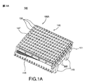
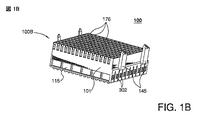
図1Aおよび1Bは、ボールグリッド側100A(図1Aで最良に見える)およびレセプタクル側100B(図1Bで最良に見える)を有するこの発明によるボールグリッドアレイ(「BGA」)コネクタ100の一実施例を描いている。ここに記述されたコネクタは、ボールグリッドアレイコネクタとして描かれているが、BGA以外の、スルーピン実装、または面実装を使用することができることは、理解されるべきである。図示されるように、BGAコネクタ100は、ハウジング101を有することができ、それは、例えば内部空洞を規定するプラスチックのような電気絶縁材料から作ることができる。このハウジング101は、1つまたはそれ以上のインサート成形されたリードフレーム組立体(「IMLA」)115を収容することができる。一実施例において、ハウジング101は、あらゆる数のIMLA 115を収容することができることは理解されるべきであるが、このハウジング101は、10個のIMLA 115を収容することができる。   1A and 1B illustrate one embodiment of a ball grid array (“BGA”) connector 100 according to the present invention having a ball grid side 100A (best seen in FIG. 1A) and a receptacle side 100B (best seen in FIG. 1B). I'm drawing. Although the connectors described herein are depicted as ball grid array connectors, it should be understood that through-pin mounting or surface mounting other than BGA can be used. As shown, the BGA connector 100 can have a housing 101, which can be made from an electrically insulating material, such as plastic, that defines an internal cavity, for example. The housing 101 can contain one or more insert molded leadframe assemblies (“IMLA”) 115. In one embodiment, it should be understood that the housing 101 can accommodate any number of IMLAs 115, but the housing 101 can accommodate ten IMLAs 115.

図2は、IMLA 115の一実施例を描いている。図示されるように、IMLA 115は、1組の1つまたはそれ以上の、重ね成形されたハウジング215を通って延びる電気伝導性接点211を有することができる。この重ね成形されたハウジング215は、例えばプラスチックのような電気絶縁材料から作ることができる。差動信号対を形成する隣接した接点211は、対を形成する接点間のほぼ一定の差動インピーダンスプロファイルを維持するためにそれらが重ね成形されたハウジング215を通って延びながら、相互に向って、または遠ざかるようにジョグすることができる。行内への配置のために、接点211は、重ね成形されたハウジング215の長さに沿って(例えば、図2に示されるように「Y」方向に沿って)配置することができる。「Y」方向に延びる重ね成形されたハウジング215の長さは、「X」または「Z」方向のいずれかに延びる重ね成形されたハウジング215の長さより長い。「Y」方向に延びる長さは、以下に「リードフレーム方向」として参照される。すなわち、「リードフレーム方向」は、重ね成形されたハウジング215がその最長の軸(例えば「Y」軸)上で延びている方向を意味する。   FIG. 2 depicts one embodiment of IMLA 115. As shown, the IMLA 115 can have a set of one or more electrically conductive contacts 211 that extend through the overmolded housing 215. The overmolded housing 215 can be made from an electrically insulating material such as plastic. Adjacent contacts 211 forming the differential signal pair are directed toward each other while they extend through the overmolded housing 215 to maintain a substantially constant differential impedance profile between the contacts forming the pair. Or jog away. For placement in a row, the contacts 211 can be placed along the length of the overmolded housing 215 (eg, along the “Y” direction as shown in FIG. 2). The length of the overmolded housing 215 extending in the “Y” direction is longer than the length of the overmolded housing 215 extending in either the “X” or “Z” direction. The length extending in the “Y” direction will be referred to as “lead frame direction” below. That is, the “lead frame direction” means a direction in which the overmolded housing 215 extends on its longest axis (eg, “Y” axis).

接点211は、例えば、2重のビームレセプタクル接点であることができる。   The contact 211 can be, for example, a double beam receptacle contact.

そのような2重のビームレセプタクル接点は、電気装置と結合する間、補完的なビーム接点を受けるように適応される。図2に示されるように、各接点211は、2重のビームレセプタクル部分217と端子部216とを有することができる。端子部216は、以下に述べるように、ハンダボール120を受入れるように適応されることができる。 Such dual beam receptacle contacts are adapted to receive complementary beam contacts while coupled to an electrical device. As shown in FIG. 2, each contact 211 can have a double beam receptacle portion 217 and a terminal portion 216. The terminal portion 216 can be adapted to receive a solder ball 120 as described below.

IMLA 115は、さらに、1つまたはそれ以上の収容タブ204を有することができる。一実施例においては、それぞれのタブ204は、IMLA 115の各端部に配置されることができる。例えば、IMLA 115の終端における接点211は、重ね成形されたハウジング215のフェース面を越えて延びるタブ204を有することができる。そのような実施例においては、タブ204は、接点211と同じ材料(例えば、電気伝導材料)から作られることができる。あるいは、タブ204は、重ね成形されたハウジング215から延びることができ、さらに重ね成形されたハウジング215に取付けられるか、または重ね成形されたハウジング215と一体に形成されることもできる。そのような実施例においては、タブ204は、重ね成形されたハウジング215と同じ材料(例えば電気絶縁材料)から作られることができる。   The IMLA 115 can further have one or more receiving tabs 204. In one embodiment, each tab 204 can be disposed at each end of IMLA 115. For example, the contacts 211 at the end of the IMLA 115 can have tabs 204 that extend beyond the face surface of the overmolded housing 215. In such embodiments, tab 204 can be made from the same material as contact 211 (eg, an electrically conductive material). Alternatively, the tab 204 can extend from the overmolded housing 215 and can be attached to the overmolded housing 215 or integrally formed with the overmolded housing 215. In such embodiments, the tab 204 can be made from the same material (eg, an electrically insulating material) as the overmolded housing 215.

図3に最良に見られるように、コネクタハウジング101は、1つまたはそれ以上のタブレセプタクル302を有することができる。一実施例において、タブレセプタクル302のそれぞれの対は、ハウジング101の対向する両側に配置されて、第1方向(図3に示されるY方向のような)に、関連するIMLA 115を収容する。各タブレセプタクル302は、それぞれのタブ204を受入れるための開口322を有することができる。そのような開口はそれぞれ、タブレセプタクル内に形成された複数のフェース面332によって規定することができる。タブレセプタクル302は、それらがハウジング101内に、関連するIMLA 115を挿入するのに十分に変位されるように、弾力性がある。ハウジング101内に挿入されたIMLA 115によって、タブレセプタクル302は、跳ね返り、したがって、タブ204は、タブレセプタクル302における開口322内に設定することができる。この発明の態様によれば、タブレセプタクル302は、あらゆる方向にハウジング内にIMLAを収容することができ、さらに、ハウジング内にあらゆる方向にIMLA 115の移動を考慮することができる。   As best seen in FIG. 3, the connector housing 101 can have one or more tab receptacles 302. In one embodiment, each pair of tab receptacles 302 is disposed on opposite sides of the housing 101 to accommodate an associated IMLA 115 in a first direction (such as the Y direction shown in FIG. 3). Each tab receptacle 302 can have an opening 322 for receiving a respective tab 204. Each such opening can be defined by a plurality of face surfaces 332 formed in the tab receptacle. The tab receptacles 302 are resilient so that they are sufficiently displaced to insert the associated IMLA 115 into the housing 101. With the IMLA 115 inserted into the housing 101, the tab receptacle 302 rebounds, and thus the tab 204 can be set in the opening 322 in the tab receptacle 302. According to aspects of the present invention, the tab receptacle 302 can accommodate the IMLA in the housing in any direction, and can allow for movement of the IMLA 115 in any direction within the housing.

Y方向にIMLA 115の移動を可能とするために、リードフレーム215は、レセプタクル302の内表面305までずっと延びる必要はない。重ね成形されたハウジング215の端部が、関連するタブレセプタクル302の内表面305に接触するときには、タブレセプタクル302は、重ね成形されたハウジング215がY方向にそれ以上移動することを防ぐ。IMLA 115が、Y方向におけるハウジング101に関して移動できる距離は、重ね成形されたハウジング215の端部とハウジング101の内表面305との間の距離を規制することによって制御することができる。したがって、タブレセプタクル302は、ハウジング101内のY方向にIMLA 115を収容することができ、その間、Y方向にIMLAの移動を可能にする。   The lead frame 215 need not extend all the way to the inner surface 305 of the receptacle 302 to allow movement of the IMLA 115 in the Y direction. When the end of the overmolded housing 215 contacts the inner surface 305 of the associated tab receptacle 302, the tab receptacle 302 prevents the overmolded housing 215 from moving further in the Y direction. The distance that the IMLA 115 can move relative to the housing 101 in the Y direction can be controlled by regulating the distance between the end of the overmolded housing 215 and the inner surface 305 of the housing 101. Thus, the tab receptacle 302 can accommodate the IMLA 115 in the Y direction within the housing 101 while allowing the IMLA to move in the Y direction.

X方向およびZ方向にハウジング101に関してIMLA 115の移動を可能にするために、レセプタクル開口322は、この開口322が受入れるように適応されるタブ204の断面(X−Z平面における)よりもわずかに大きくすることができる。タブ204がフェース面332のうちの1つに接触するときに、フェース面332は、IMLA 115が移動(例えばX方向またはZ方向に)している方向にでもタブ204(かつ、したがって重ね成形されたハウジング215)が幾分かさらに移動するのを防ぐ。レセプタクル開口322とタブ204の断面との間の寸法における相対的な差が、IMLA 115が、X方向およびZ方向にハウジング101に関して、移動することができる量を決定する。したがって、X−Z平面においてIMLAの移動を可能にする間、タブレセプタクル302は、X方向およびZ方向にIMLA 115を収容することができる。   In order to allow movement of the IMLA 115 relative to the housing 101 in the X and Z directions, the receptacle opening 322 is slightly less than the cross section (in the XZ plane) of the tab 204 that this opening 322 is adapted to receive. Can be bigger. When the tab 204 contacts one of the face surfaces 332, the face surface 332 is also tab 204 (and thus overmolded) in the direction in which the IMLA 115 is moving (eg, in the X or Z direction). The housing 215) is prevented from moving somewhat further. The relative difference in dimensions between the receptacle opening 322 and the cross section of the tab 204 determines the amount that the IMLA 115 can move relative to the housing 101 in the X and Z directions. Thus, the tab receptacle 302 can accommodate the IMLA 115 in the X and Z directions while allowing IMLA movement in the XZ plane.

この発明の一実施例において、タブ204は、Z方向に約0.20mmの、そしてX方向に約1.30mmの寸法を有することができる。レセプタクル開口322は、X方向に約0.23mmの、そしてZ方向に約1.45mmの寸法を有することができる。この重ね成形されたハウジング215の各端部とハウジング101のそれぞれの内表面305との間の距離は、約0.3mmであることができる。   In one embodiment of the present invention, the tab 204 may have a dimension of about 0.20 mm in the Z direction and about 1.30 mm in the X direction. Receptacle opening 322 may have a dimension of about 0.23 mm in the X direction and about 1.45 mm in the Z direction. The distance between each end of the overmolded housing 215 and the respective inner surface 305 of the housing 101 can be about 0.3 mm.

図1Aおよび1Bに示されるように、この発明によるコネクタ100は、ボールグリッドアレイ148を有することができる。このボールグリッドアレイ148は、それぞれの電気接点211の端子端部216においてそれぞれのハンダボール120を形成することによって形成することができる。したがって、このボールグリッドアレイコネクタ100は、例えばボールグリッドアレイ148に補完的であるパッドアレイを有して、プリント回路基板のような基板上に設定することができる。   As shown in FIGS. 1A and 1B, a connector 100 according to the present invention may have a ball grid array 148. The ball grid array 148 can be formed by forming each solder ball 120 at the terminal end 216 of each electrical contact 211. Thus, the ball grid array connector 100 can be set on a board, such as a printed circuit board, having a pad array that is complementary to the ball grid array 148, for example.

この発明の態様によれば、コネクタ100は、端子端部の移動を可能にしていると同時に、接点の端子端部を有する接点受入れ基板またはウェーハ107を有することができる。ウェーハ107は、例えばプラスチックのような電気絶縁材料から作られることができる。   According to this aspect of the invention, the connector 100 can have a contact-receiving substrate or wafer 107 having a terminal end of the contact while simultaneously allowing movement of the terminal end. Wafer 107 can be made of an electrically insulating material such as plastic.

図4に最良に見られるように、このウェーハ107は、アレイ状の孔456を有することができる。各孔456は、それぞれの接点211のそれぞれの終端部216を受入れることができる。各孔456は、X方向およびY方向に端子を収容するフェース面478のそれぞれの組によって規定される。X方向およびY方向に端子の移動を可能にするために、孔456は、孔456が受入れるように適応される端子216の断面(X−Y平面における)よりもわずかに大きいということができる。図示されるように、フェース面の少なくとも1つが接点の幅より大きい長さを有するように、フェース面478は、その孔456を規定することができる。したがって、接点の端子部は、自由に位置することができるか、または孔456内に、「浮かぶ」。すなわち、接点の端子部は、孔456を規定するあらゆるフェース面と必ずしも接触する必要はない。孔456と端子216との間の寸法の相対的な差は、その端子がX方向およびY方向に移動することができる量を決定する。したがって、X−Y平面において端子部216の移動を可能にしている間に、ウェーハ107は、X方向およびZ方向に接点211の端子部216を収容することができる。   As best seen in FIG. 4, the wafer 107 can have an array of holes 456. Each hole 456 can receive a respective termination 216 of a respective contact 211. Each hole 456 is defined by a respective set of face surfaces 478 that accommodate terminals in the X and Y directions. In order to allow movement of the terminal in the X and Y directions, the hole 456 may be slightly larger than the cross-section (in the XY plane) of the terminal 216 that the hole 456 is adapted to receive. As shown, the face surface 478 can define its hole 456 such that at least one of the face surfaces has a length greater than the width of the contact. Thus, the terminal portion of the contact can be freely positioned or “float” within the hole 456. In other words, the terminal portion of the contact does not necessarily need to contact every face surface that defines the hole 456. The relative difference in dimensions between hole 456 and terminal 216 determines the amount that the terminal can move in the X and Y directions. Accordingly, the wafer 107 can accommodate the terminal portions 216 of the contacts 211 in the X direction and the Z direction while allowing the terminal portions 216 to move in the XY plane.

図示されるように、孔456があらゆる所望の形状を有すると規定されることができることは理解されるべきであるが、孔456は、一般に長方形であることができる。この発明の一実施例において、接点部211の端子部216は、約0.2mm掛ける約0.3mmの寸法を有することができる。孔456は、約0.6mm掛ける約0.6mmの寸法を有することができる。   As shown, it should be understood that the hole 456 can be defined to have any desired shape, but the hole 456 can be generally rectangular. In one embodiment of the present invention, the terminal portion 216 of the contact portion 211 may have a dimension of about 0.3 mm multiplied by about 0.2 mm. The hole 456 may have a dimension of about 0.6 mm times about 0.6 mm.

コネクタ100を製造するために、IMLA 115は、上述されたように、ハウジング101内に挿入されて、ラッチされることができる。その後、ウェーハ107は、孔456内に延びる接点211の端子部216によって、重ね成形されたハウジング215のボール側表面229上に設定されることができる。その後、それぞれのハンダボール120は、既知の技術を使用して、接点211の端子部216上に形成されることができる。図5は、重ね成形されたハウジング215を通って延びる接点211のそれぞれの端子部216上に形成された複数のハンダボール120を描いている。ウェーハ107が、ハンダボール120が形成される前にリードフレーム上に設置されるであろうことが熟考されるけれども、図5は、ハンダボール120を備えるが、ウェーハ107は備えないコネクタを、描いていることに注意されたい。
接点211の端子部216上にハンダボール120を形成するために、ハンダペーストは、接点211の端子部216がその中に延びる孔456内に置かれることができる。ハンダボール120は、ウェーハ107の表面に対してハンダペースト内に押圧されることができる。孔を通して接点211がハウジング内に引かれるのを防ぐために、ハンダボール120の直径は、孔456の幅より大きいということができる。コネクタ組立体(それは、少なくとも、ハウジング101とウェーハ107とを結合した接点211を有している)は、ハンダの液化温度よりも高い温度に加熱されることができる。このことは、ハンダをリフローさせ、接点端子部216上に球形に形づくられたハンダのかたまりを形成し、接点211にハンダボール120を冶金学的に接合する。
To manufacture the connector 100, the IMLA 115 can be inserted into the housing 101 and latched as described above. Thereafter, the wafer 107 can be set on the ball-side surface 229 of the overmolded housing 215 by the terminal portion 216 of the contact 211 extending into the hole 456. Thereafter, each solder ball 120 can be formed on the terminal portion 216 of the contact 211 using known techniques. FIG. 5 depicts a plurality of solder balls 120 formed on each terminal portion 216 of the contact 211 that extends through the overmolded housing 215. Although it is contemplated that the wafer 107 will be placed on the lead frame before the solder ball 120 is formed, FIG. Please note that.
To form the solder ball 120 on the terminal portion 216 of the contact 211, the solder paste can be placed in the hole 456 into which the terminal portion 216 of the contact 211 extends. The solder balls 120 can be pressed into the solder paste against the surface of the wafer 107. In order to prevent the contact 211 from being pulled through the hole and into the housing, the diameter of the solder ball 120 can be said to be greater than the width of the hole 456. The connector assembly (which has at least a contact 211 that couples the housing 101 and the wafer 107) can be heated to a temperature higher than the liquefaction temperature of the solder. This reflows the solder, forms a spherical solder piece on the contact terminal portion 216, and metallurgically joins the solder ball 120 to the contact 211.

好ましくは、孔456は、ハンダボール120が、接点211がハウジング101に引かれる可能性があるのを防ぐように、ハンダボール120の直径未満である幅を有する。同様に、ハンダボール120の直径が孔456の幅より大きいので、ウェーハ107が、ハンダボール120とIMLA 115の重ね成形されたハウジング215との間に収容されることができる。   Preferably, the hole 456 has a width that is less than the diameter of the solder ball 120 to prevent the solder ball 120 from being pulled into the housing 101. Similarly, because the diameter of the solder ball 120 is larger than the width of the hole 456, the wafer 107 can be received between the solder ball 120 and the overmolded housing 215 of IMLA 115.

図6に示されるように、コネクタハウジング101は、さらに1つまたはそれ以上のハンダポスト160を有することができる。ハンダポスト160は、ハンダまたはハンダづけすることができる表面を収容することができるが、PCB基板によって規定されたオリフィス内に受入れられるように適応されることができる。   As shown in FIG. 6, the connector housing 101 can further include one or more solder posts 160. The solder post 160 can accommodate solder or a solderable surface, but can be adapted to be received within an orifice defined by a PCB substrate.

ハンダボール120のリフローに先立って、上述されたように、IMLA 115は、ハウジング101に関して自由に移動することができる。この移動、または浮上は、ハンダボール120のリフロー中にIMLA 115が自己整列する可能性がある。例えば、ハンダボール120がリフロー中に液化するときに、液状ハンダにおける表面張力は、自動整列の効果を生じる。この発明は、IMLA 115が液状ハンダボール120の自動整列する特性から利益を得ることを可能にする。一旦リフローが完了すると、接点211と、ハウジング101と、ハンダポスト160とは、PCBに関して固定される。固定されたハンダポスト160は、PCBに平行な方向に、ハウジング101に作用する力がハンダボール120に伝わるのを阻止するのを支援する。 Prior to reflow of the solder balls 120, the IMLA 115 is free to move with respect to the housing 101, as described above. This movement, or levitation, can cause IMLA 115 to self-align during reflow of solder balls 120. For example, when the solder balls 120 are liquefied during reflow, the surface tension in the liquid solder produces an automatic alignment effect. The present invention allows IMLA 115 to benefit from the self-aligning properties of liquid solder balls 120. Once reflow is complete, the contacts 211, housing 101, and solder post 160 are secured with respect to the PCB. The fixed solder post 160 assists in preventing forces acting on the housing 101 from being transmitted to the solder balls 120 in a direction parallel to the PCB.

図7は、この発明によるBGAコネクタ500の他の一実施例の斜視図を提供する。図8は、この発明によるウェーハ507の他の一実施例の平面図を提供する。コネクタ500は、ボールグリッドアレイ側から図示されている。ここに記述されたコネクタ500は、BGAコネクタとして描かれているが、BGA以外に、スルーピン実装、または表面実装が使用できることが理解されるべきである。コネクタ500は、ハウジング501と、1つまたはそれ以上のIMLAまたはステッチ接点(図示せず)と、接点受け基板またはウェーハ507とを有することができる。ウェーハ507は、ハンダパッドの移動を考慮に入れる間に、ここに記述された接点211の端子部216のような接点の端子端部を有することができる。このウェーハ507は、例えばプラスチックのような電気絶縁材料で作ることができる。   FIG. 7 provides a perspective view of another embodiment of a BGA connector 500 according to the present invention. FIG. 8 provides a top view of another embodiment of a wafer 507 according to the present invention. The connector 500 is shown from the ball grid array side. Although the connector 500 described herein is depicted as a BGA connector, it should be understood that through-pin mounting or surface mounting can be used in addition to BGA. The connector 500 can include a housing 501, one or more IMLA or stitch contacts (not shown), and a contact receiving substrate or wafer 507. Wafer 507 may have a terminal end of a contact, such as terminal 216 of contact 211 described herein, while taking into account the movement of solder pads. The wafer 507 can be made of an electrically insulating material such as plastic.

図8に最良に見られるように、ウェーハ507は、ウェーハ107に関してここに記述された孔456に近似している接点受入孔556のアレイを有することができる。PCBに対するコネクタのリフロー中に、接点の端子端部の相対的移動を可能にするために、接点受入孔556は、孔556が受入れるように適応される接点の端子端部の断面よりわずかに大きいということができる。したがって、各接点の端子部は、自由に位置するか、またはそれぞれの孔556内に「浮かぶ」ことができる。図示されるように、孔556があらゆる所望形状をも有すると規定することができることは理解されるべきであるが、孔556は、ほぼ長方形であることができる。   As best seen in FIG. 8, the wafer 507 can have an array of contact receiving holes 556 that approximate the holes 456 described herein with respect to the wafer 107. To allow relative movement of the contact terminal end during connector reflow to the PCB, the contact receiving hole 556 is slightly larger than the cross-section of the contact terminal end that the hole 556 is adapted to receive. It can be said. Thus, the terminal portion of each contact can be freely positioned or can “float” within its respective hole 556. As shown, it should be understood that the hole 556 can have any desired shape, but the hole 556 can be generally rectangular.

ウェーハ107に関して記述されたように、IMLAまたは他の表面実装接点尾部は、ハウジング501に挿入されることができ、また、ウェーハ507は、孔556に延びる接点の端子部とともにIMLAの重ね成形されたハウジング上に設置することができる。その後、それぞれのハンダボール520は、接点の端子部上に形成されることができる。   As described with respect to wafer 107, IMLA or other surface mount contact tails can be inserted into housing 501 and wafer 507 is overlaid with IMLA with contact terminals extending into holes 556. It can be installed on the housing. Thereafter, each solder ball 520 can be formed on the terminal portion of the contact.

ウェーハ507は、Y方向(図8に関して示されるように)に、すなわちIMLAのリードフレーム方向とほぼ平行な方向に延びる可撓性部材560の直線アレイを有することができる。図2に関して記述されたように、「リードフレーム方向」は、IMLAの重ね成形されたハウジングがその最長の軸(例えば、「Y」軸、または「Y」方向に沿って)上で延びる方向を指す。ウェーハ507は、リードフレーム方向(Y方向)に延びる2つの短い平行側、および、リードフレーム方向(X方向)に直交方向に延長する2つの長い平行側によって、矩形形状であることができる。   Wafer 507 may have a linear array of flexible members 560 extending in the Y direction (as shown with respect to FIG. 8), ie, in a direction substantially parallel to the IMLA leadframe direction. As described with respect to FIG. 2, the “lead frame direction” refers to the direction in which the IMLA overmolded housing extends on its longest axis (eg, along the “Y” axis, or along the “Y” direction). Point to. The wafer 507 can have a rectangular shape with two short parallel sides extending in the lead frame direction (Y direction) and two long parallel sides extending in a direction orthogonal to the lead frame direction (X direction).

可撓性部材560の直線的アレイは、2つのウェーハ本体部分508、509内に、リードフレーム方向に直交して、X方向に、ウェーハ507を区分することができる。すなわち、可撓性部材560は、その最長の方向にウェーハ507を区分することができる。可撓性部材560は、あらゆる所望形状および寸法であることができる。図7および8に描かれている一実施例において、5つの可撓性部材560は、それぞれ、ほぼ「S」形であることができる。ウェーハ507は、可撓性部材560を作成するために適切な形状および寸法の曲げ生成孔562を規定することができる。   The linear array of flexible members 560 can partition the wafer 507 in the X direction, perpendicular to the lead frame direction, in the two wafer body portions 508, 509. That is, the flexible member 560 can section the wafer 507 in the longest direction. The flexible member 560 can be any desired shape and size. In one embodiment depicted in FIGS. 7 and 8, each of the five flexible members 560 can be generally “S” shaped. Wafer 507 can define bend generation holes 562 of an appropriate shape and size to create flexible member 560.

この孔562の形状および対応する可撓性部材560の形状に加えて、曲げ生成孔562を規定することにおけるウェーハ507の材料の除去は、PCBの移動に応答するようにウェーハ507の能力を提供することができる。すなわち、可撓性部材560の形状(または曲げ生成孔562の形状)は、ウェーハ部分508、509が、ウェーハ507を膨張するか収縮するかして、ほぼX方向に、移動することを可能にすることができる。   In addition to the shape of this hole 562 and the corresponding shape of the flexible member 560, removal of the material of the wafer 507 in defining the bend generating hole 562 provides the ability of the wafer 507 to respond to PCB movement. can do. That is, the shape of the flexible member 560 (or the shape of the bend generation hole 562) allows the wafer portions 508, 509 to move substantially in the X direction as the wafer 507 expands or contracts. can do.

膨張するか収縮するそのような能力は、PCBに接続されたハンダボール120に別の方法でかけられる圧力を逃げることができる。そのような圧力は、PCB/コネクタ装置の正常な使用の間に、例えば温度変動によって生じる。この温度変動は、コネクタ500、またはコネクタ500の一部分と、コネクタ500が接続されるPCBとの間において、熱膨脹係数(CTE)における誤った組合せのために圧力を生じる。例えば、コネクタ500およびPCBが正常な使用の間に加熱されるとともに、コネクタ500は、X方向にPCBより急速に膨張することがある。ハンダボール/接続120は、移動しなくてもよいか、あるいはIMLAから延びるハンダ接続の剰余の部分(remainder)よりゆっくり外方に移動する。さらに例えば、コネクタ500およびPCBが正常な使用の間に加熱されるので、PCBは、X方向に、より急速に膨張し、コネクタ500、また、したがって、ハンダボール120は、IMLAから延びるハンダボール120の剰余の部分より急速に移動する。反対に、コネクタ500およびPCBが冷却すると、それぞれは、他方と異なる率で収縮し、その結果コネクタ500とPCBハンダ接続の間の相対的移動を引き起こす。可撓性部材560は、ウェーハ507がPCBにおける移動中のハンダパッドとして膨張するか収縮するかを可能にして、ハンダボール移動120に応答することができる。そのような膨張あるいは短縮は、PCBとの接続点においてハンダボール120に対する圧力をかけるのを防止するのを支援することができる。ウェーハ507が、このように膨張し収縮することを可能にすることは、PCB接続に対する圧力を減少し、かつ熱サイクルにもかかわらずコネクタ500の機能的な寿命を伸ばすのを支援することができる。   Such ability to expand or contract can relieve pressure otherwise applied to the solder balls 120 connected to the PCB. Such pressure occurs during normal use of the PCB / connector device, for example due to temperature fluctuations. This temperature variation creates pressure due to an incorrect combination of coefficient of thermal expansion (CTE) between the connector 500 or a portion of the connector 500 and the PCB to which the connector 500 is connected. For example, as the connector 500 and the PCB are heated during normal use, the connector 500 may expand more rapidly than the PCB in the X direction. The solder balls / connections 120 may not move or move outward slowly from the remainder of the solder connection extending from the IMLA. Further, for example, because the connector 500 and the PCB are heated during normal use, the PCB expands more rapidly in the X direction, and the connector 500, and therefore the solder ball 120, also extends from the IMLA. Move more rapidly than the remainder. Conversely, when the connector 500 and the PCB cool, each contracts at a different rate than the other, resulting in a relative movement between the connector 500 and the PCB solder connection. The flexible member 560 can respond to the solder ball movement 120 by allowing the wafer 507 to expand or contract as a moving solder pad on the PCB. Such expansion or shortening can help prevent pressure on the solder ball 120 at the connection point with the PCB. Allowing the wafer 507 to expand and contract in this manner can help reduce pressure on the PCB connection and extend the functional life of the connector 500 despite thermal cycling. .

ウェーハ507が、Y方向に、すなわちリードフレーム方向に平行で、またはX方向およびY方向の組合せ方向に、膨張するか収縮するかを可能にするために、可撓性部材560が形づくられ、寸法採りされ、方向付けすることができることは、理解されるべきである。さらに、理解されるべきであるのは、ウェーハ507は、直線アレイに5つの可撓性部材560を有し(そして6つの曲げ生成孔562を規定し)ているが、あらゆる数の可撓性部材560または孔562が、圧力を逃げるために使用でき、また他の実施例は、その中において可撓性部材560および孔562が、異なる形状であり、寸法であると想像され、また、直線アレイ内以外の、集積装置内に延びる。さらに、可撓性部材560の厚さは、ウェーハ507の厚さより小さいか、より大きいということができることは理解されるべきである。さらに、1つより多い直線アレイの使用も想像される。   A flexible member 560 is shaped and dimensioned to allow the wafer 507 to expand or contract in the Y direction, ie parallel to the lead frame direction, or in the combined direction of the X and Y directions. It should be understood that it can be taken and directed. Further, it should be understood that wafer 507 has five flexible members 560 in a linear array (and defines six bend generation holes 562), but any number of flexible members. Member 560 or hole 562 can be used to relieve pressure, and other embodiments are envisioned in which flexible member 560 and hole 562 are of different shapes and dimensions, and linear It extends into the integrated device other than within the array. Further, it should be understood that the thickness of the flexible member 560 can be less than or greater than the thickness of the wafer 507. In addition, the use of more than one linear array is envisioned.

この発明によれば、図9は、代りの実施例ウェーハ607の平面図を提供する。このウェーハ607は、前記ウェーハ507に関してここに記述された孔556に近似する接点受入孔656のアレイを有することができる。PCBに対するコネクタのリフロー中に接点の端子端部の移動を可能にするために、孔656は、その孔656が受入れるように適応される接点の端子端部の断面よりもわずかに大きいということができる。したがって、各接点の端子部は、孔656内に自由に位置するか、または「浮かぶ」ことができる。図示されるように、孔656があらゆる所望の形状を有すると規定されることができることは理解されるべきであるが、その孔656は、ほぼ長方形であることができる。   In accordance with the present invention, FIG. 9 provides a top view of an alternative embodiment wafer 607. The wafer 607 can have an array of contact receiving holes 656 that approximate the holes 556 described herein with respect to the wafer 507. In order to allow movement of the terminal end of the contact during reflow of the connector to the PCB, the hole 656 is slightly larger than the cross-section of the contact terminal end that the hole 656 is adapted to receive. it can. Thus, the terminal portion of each contact can be freely located or “float” in the hole 656. As shown, it should be understood that the hole 656 can be defined as having any desired shape, but the hole 656 can be generally rectangular.

ウェーハ507に関して記述されたように、ウェーハ607は、孔656内に延びるIMLA接点の端子部とともに、コネクタのハウジング、またはIMLAの重ね成形したハウジング上に設置されるように配置されることができる。リードフレームの方向は、図9に示されるように「Y」方向にあることができる。その後、それぞれのハンダボールは、接点の端子部上に形成されて、ウェーハ607を有することができる。   As described with respect to wafer 507, wafer 607 can be positioned to be placed on the connector housing or IMLA overmolded housing with the terminal portion of the IMLA contact extending into hole 656. The direction of the lead frame can be in the “Y” direction as shown in FIG. Thereafter, each solder ball can be formed on a contact terminal and have a wafer 607.

ウェーハ607は、リードフレームの方向(Y方向)に延びる2つの短い平行側、および、リードフレームの方向(X方向)に直交して延びる2つの長い平行側によって、長方形であることができる。   The wafer 607 may be rectangular with two short parallel sides extending in the lead frame direction (Y direction) and two long parallel sides extending perpendicular to the lead frame direction (X direction).

ウェーハ607は、X方向でリードフレーム方向に直交して延びる可撓性部材660の2つの直線アレイを有することができる。可撓性部材660の直線アレイは、そのより短いY方向にウェーハ607を3つの区域608、609、610に区分することができる。可撓性部材660は、あらゆる適切な形状および寸法であることができる。図9に描かれている一実施例において、可撓性部材660は、ほぼ「L」形状であることができる。ウェーハ607は、可撓性部材560を生成するために適切な形状および寸法の曲げ生成孔662を規定することができる。   Wafer 607 can have two linear arrays of flexible members 660 extending in the X direction and perpendicular to the lead frame direction. The linear array of flexible members 660 can partition the wafer 607 into three sections 608, 609, 610 in its shorter Y direction. The flexible member 660 can be any suitable shape and size. In one example depicted in FIG. 9, the flexible member 660 can be generally “L” shaped. Wafer 607 can define bend generation holes 662 of suitable shape and dimensions to produce flexible member 560.

曲げ生成孔662を規定するウェーハ607の材料の除去は、孔662の形状および可撓性部材660の対応する形状に加えて、ウェーハ607がハンダ接続の移動に対応する能力を提供することができる。すなわち、可撓性部材660の形状(または曲げ生成孔662の形状)は、ウェーハ部分608、609、610が、ウェーハ607を膨張するかまたは収縮して、ほぼY方向に、移動することを可能にすることができる。可撓性部材660は、「L」形状部材660を曲げるか引く傾向があるY方向に平行に、及ぼされたせん断力に少なくとも部分的に反応することができる。この「L」形状の可撓性部材660は、ハンダパッドの移動によって、例えば、ウェーハ607が及ぼされた膨張力に通常に反応することを可能にして、そのようなせん断力に反応することができる。各可撓性部材660は、「L」形状を圧縮する傾向があるY方向に平行に、少なくとも部分的に、及ぼされたせん断力にさらに反応することができる。「L」形状の可撓性部材660は、ウェーハ607がハンダパッドの移動によって及ぼされた収縮力に反応することを可能にして、圧縮力に反応することができる。   Removal of the material of the wafer 607 defining the bend generation hole 662 can provide the ability of the wafer 607 to accommodate the movement of the solder connection, in addition to the shape of the hole 662 and the corresponding shape of the flexible member 660. . That is, the shape of the flexible member 660 (or the shape of the bend generation hole 662) allows the wafer portions 608, 609, 610 to move substantially in the Y direction as the wafer 607 expands or contracts. Can be. The flexible member 660 can be at least partially responsive to shear forces exerted parallel to the Y direction that tends to bend or pull the “L” shaped member 660. This “L” shaped flexible member 660 can react to such shear forces by allowing the solder pad movement to react normally to, for example, the expansion force exerted on the wafer 607. it can. Each flexible member 660 can be further responsive to applied shear forces, at least partially, parallel to the Y direction that tends to compress the “L” shape. The “L” shaped flexible member 660 can react to the compressive force, allowing the wafer 607 to react to the contraction force exerted by the movement of the solder pad.

膨張するか収縮するそのような能力は、別のやり方では、PCBに接続された電気コネクタのハンダボールまたはハンダ接続にかけられる圧力を逃げることができる。そのような圧力は、PCB/コネクタシステムの正常な使用の間に温度変動によって引き起こされる。この温度変動は、ハンダボール120とPCBのハンダパッドとの間のCTEの誤った組合せのために圧力を引き起こす。ウェーハ607が膨張し収縮することを可能にすることは、PCB接続における圧力を減少し、かつ、熱サイクルにかかわらずコネクタの機能的な寿命を延ばすのを支援することができる。   Such ability to expand or contract can otherwise relieve the pressure applied to the solder balls or solder connections of the electrical connectors connected to the PCB. Such pressure is caused by temperature fluctuations during normal use of the PCB / connector system. This temperature variation causes pressure due to an incorrect combination of CTEs between the solder balls 120 and the PCB solder pads. Allowing the wafer 607 to expand and contract can reduce the pressure at the PCB connection and help to extend the functional life of the connector regardless of thermal cycling.

理解されるであろうことは、あらゆる数の可撓性部材660の直線アレイ、または曲げ生成孔662が、圧力を逃げるために使用することができ、さらに、代りの実施例は、可撓性部材660または曲げ生成孔662が、異なる形状および寸法であり、直線アレイ内以外の集積回路装置内に延びる予想をすることができる。さらに理解されるべきことは、可撓性部材660の厚さは、ウェーハ607の厚さよりも小さいかまたは大きいということができる。   It will be appreciated that any number of linear arrays of flexible members 660, or bend generating holes 662, can be used to relieve pressure, and alternative embodiments are flexible. It can be envisaged that member 660 or bend generation hole 662 is of a different shape and size and extends into an integrated circuit device other than within a linear array. It should be further understood that the thickness of the flexible member 660 is less than or greater than the thickness of the wafer 607.

先行の例証的実施例は、単に説明の目的で提供されており、発明の限定として全く解釈されないことになっていることは理解されるべきである。ここに使用された用語は、内容表示文言ではなく、記述と描画の文言である。さらに、この発明は、特別の構造、材料およびまたは実施例に関してここに記述されたが、この発明は、ここに示された詳細に制限されるようには意図されていない。むしろ、この発明は、付属する請求項の範囲内であるようなあらゆる機能的に等価の構成、方法および用途に拡張する。この明細書の教示の利益を有する技術に熟練している者は、それに対する多数の改良に影響され、また、変更は、その態様におけるこの発明の範囲および精神から逸脱することなく行うことができる。   It should be understood that the preceding illustrative examples are provided for illustrative purposes only and are not to be construed as limiting the invention in any way. The terminology used here is not a content display wording but a description and drawing wording. Further, although the invention has been described herein with reference to particular structures, materials and / or examples, the invention is not intended to be limited to the details shown. Rather, the present invention extends to any functionally equivalent arrangement, method and application that is within the scope of the appended claims. Those skilled in the art having the benefit of the teachings of this specification will be affected by numerous improvements thereto, and modifications may be made without departing from the scope and spirit of the invention in its embodiments. .

この発明による電気コネクタの一実施例を描いている。1 illustrates one embodiment of an electrical connector according to the present invention. この発明による電気コネクタの一実施例を描いている。1 illustrates one embodiment of an electrical connector according to the present invention. この発明によるインサート成形されたリードフレーム組立体の一実施例を描いている。1 illustrates one embodiment of an insert molded leadframe assembly according to the present invention. ウェーハまたはハンダボールなしで、この発明によるボールグリッドアレイコネクタの一実施例の部分図を提供する。FIG. 4 provides a partial view of one embodiment of a ball grid array connector according to the present invention without a wafer or solder ball. ハンダボールなしで、この発明によるボールグリッドアレイコネクタの一実施例の部分図を提供する。FIG. 4 provides a partial view of one embodiment of a ball grid array connector according to the present invention without solder balls. ウェーハなしで、複数の電気接点において形成されたボールグリッドアレイの部分図を提供する。FIG. 4 provides a partial view of a ball grid array formed at a plurality of electrical contacts without a wafer. ハウジングに取付けられたハンダポストを備えたこの発明によるコネクタの斜視底面図を提供する。1 provides a perspective bottom view of a connector according to the present invention with a solder post attached to a housing. この発明によるBGAコネクタの他の一実施例の斜視図を提供する。FIG. 4 provides a perspective view of another embodiment of a BGA connector according to the present invention. この発明によるウェーハの一実施例の平面図を提供する。1 provides a plan view of one embodiment of a wafer according to the present invention. この発明によるウェーハの他の一実施例の平面図を提供する。FIG. 6 provides a plan view of another embodiment of a wafer according to the present invention.

Claims (20)

電気接点と、孔を規定するウェーハとを有してなり、前記電気接点は、前記孔内に延びており、前記ウェーハは、第1および第2本体部分と、この第1および第2本体部分を連結し、かつこの第1および第2本体部分の少なくとも一方の移動を可能にする可撓性部材とを有する電気コネクタ。   An electrical contact and a wafer defining a hole, the electrical contact extending into the hole, the wafer comprising first and second body portions, and the first and second body portions. And a flexible member that allows movement of at least one of the first and second body portions. 前記可撓性部材は、非導電性であり、かつ第1方向に前記第1本体部分の移動を、さらに第2方向に前記第2本体部分の移動を可能にする請求項1記載の電気コネクタ。   The electrical connector according to claim 1, wherein the flexible member is non-conductive and allows movement of the first body portion in a first direction and further movement of the second body portion in a second direction. . 前記第1方向は、前記第2方向と正反対である請求項2記載の電気コネクタ。   The electrical connector according to claim 2, wherein the first direction is opposite to the second direction. さらに、前記第1および第2方向の少なくとも一方は、前記リードフレームの方向と平行であるリードフレームを有する請求項2記載の電気コネクタ。   The electrical connector according to claim 2, further comprising a lead frame in which at least one of the first and second directions is parallel to a direction of the lead frame. さらに、前記第1および第2方向の少なくとも一方は、前記リードフレームの方向に直交するリードフレームを有する請求項2記載の電気コネクタ。   The electrical connector according to claim 2, wherein at least one of the first and second directions has a lead frame orthogonal to the direction of the lead frame. 前記ウェーハは、長方形であり、かつ前記第1および第2方向の少なくとも一方は、そのウェーハの長辺と平行である請求項2記載の電気コネクタ。   The electrical connector according to claim 2, wherein the wafer is rectangular, and at least one of the first and second directions is parallel to a long side of the wafer. 前記ウェーハは、長方形であり、かつ前記第1および第2方向の少なくとも一方は、ウェーハの長辺に直交する請求項2記載の電気コネクタ。   The electrical connector according to claim 2, wherein the wafer is rectangular, and at least one of the first and second directions is orthogonal to a long side of the wafer. 前記第1および第2本体部分の少なくとも一方は、温度変化に応じて移動する請求項1記載の電気コネクタ。   The electrical connector according to claim 1, wherein at least one of the first and second body portions moves in response to a temperature change. 前記第1および第2本体部分の少なくとも一方は、前記電気接点の移動に応じて移動する請求項1記載の電気コネクタ。   The electrical connector according to claim 1, wherein at least one of the first and second body portions moves in accordance with movement of the electrical contact. 前記可撓性部材は、「S」形状である請求項1記載の電気コネクタ。   The electrical connector according to claim 1, wherein the flexible member has an “S” shape. 前記可撓性部材は、「L」形状である請求項1記載の電気コネクタ。   The electrical connector according to claim 1, wherein the flexible member has an “L” shape. 平担な本体と、この平担な本体の少なくとも一部分が移動することを可能にするように配置された可撓性部材とを有してなり、前記平担な本体は、電気コネクタの電気接点の端子端部を受けるために配置された孔を規定する電気コネクタ用のウェーハ。   A flat body, and a flexible member arranged to allow at least a portion of the flat body to move, the flat body being an electrical contact of an electrical connector An electrical connector wafer defining a hole disposed to receive a terminal end of the connector. 前記平担な本体は、前記孔を通して電気接点を挿入することによって、さらには、前記接点にハンダボールを取付けることによって、少なくとも一部分を前記電気コネクタに収容するように適応される請求項12記載のウェーハ。   13. The flat body is adapted to receive at least a portion in the electrical connector by inserting an electrical contact through the hole and further by attaching a solder ball to the contact. Wafer. 前記平担な本体は、長方形であり、さらに、前記可撓性部材は、前記平担な本体が前記平担な本体の長辺に平行な方向に膨張するか収縮することを可能にするように配置される請求項12記載のウェーハ。   The flat body is rectangular and the flexible member further allows the flat body to expand or contract in a direction parallel to the long side of the flat body. The wafer according to claim 12, which is disposed on the wafer. 前記平担な本体は、長方形であり、さらに、前記可撓性部材は、前記平担な本体が平担な本体の長辺に直交する方向に膨張するか収縮することを可能にするように配置される請求項12記載のウェーハ。   The flat body is rectangular, and the flexible member further allows the flat body to expand or contract in a direction perpendicular to the long side of the flat body. The wafer according to claim 12, which is arranged. 前記可撓性部材は、前記平担な本体の少なくとも一部分が、前記電気接点の移動に応じて移動することを可能にする請求項12記載のウェーハ。   13. The wafer of claim 12, wherein the flexible member allows at least a portion of the flat body to move in response to movement of the electrical contact. 部分的にそこから延びる電気接点を有するリードフレーム組立体と、前記電気接点に取付けられたハンダボールと、このハンダボールと前記リードフレーム組立体との間に収容され、接点受入れ孔および曲げ生成孔を規定する ウェーハとを有してなり、前記接点は、少なくとも部分的に前記接点受入れ孔に挿入され、さらに、前記曲げ生成孔は、前記ウェーハの少なくとも一部分が、前記リードフレーム組立体に関して移動することを可能にする電気コネクタ。   A lead frame assembly having electrical contacts partially extending therefrom, a solder ball attached to the electrical contacts, and a contact receiving hole and a bending generating hole received between the solder ball and the lead frame assembly And wherein the contact is at least partially inserted into the contact receiving hole, and the bend generating hole is moved with respect to the lead frame assembly at least a portion of the wafer. Electrical connector that makes it possible. 前記ウェーハは、さらに、アレイ方向に延びる直線アレイに配置された複数の曲げ生成孔を規定し、この複数の曲げ生成孔の少なくとも一部分は、前記ウェーハの少なくとも一部分がアレイ方向に直交する方向に移動することを可能にする請求項17記載の電気コネクタ。   The wafer further defines a plurality of bend generation holes arranged in a linear array extending in the array direction, wherein at least a portion of the plurality of bend generation holes moves in a direction perpendicular to the array direction of the wafer. The electrical connector of claim 17, wherein the electrical connector is capable of. 前記リードフレーム組立体は、前記アレイ方向に平行な方向に延びる請求項18記載の電気コネクタ。   The electrical connector according to claim 18, wherein the lead frame assembly extends in a direction parallel to the array direction. 前記リードフレーム組立体は、前記アレイ方向に直交する方向に延びる請求項18記載の電気コネクタ。   The electrical connector according to claim 18, wherein the lead frame assembly extends in a direction orthogonal to the array direction.
JP2008523910A 2005-07-29 2006-07-11 Pressure relief of electrical connector at board interface Pending JP2009503784A (en)

Applications Claiming Priority (2)

Application Number Priority Date Filing Date Title
US11/193,765 US7258551B2 (en) 2005-07-29 2005-07-29 Electrical connector stress relief at substrate interface
PCT/US2006/026931 WO2007018915A2 (en) 2005-07-29 2006-07-11 Electrical connector stress relief at substrate interface

Publications (1)

Publication Number Publication Date
JP2009503784A true JP2009503784A (en) 2009-01-29

Family

ID=37694972

Family Applications (1)

Application Number Title Priority Date Filing Date
JP2008523910A Pending JP2009503784A (en) 2005-07-29 2006-07-11 Pressure relief of electrical connector at board interface

Country Status (6)

Country Link
US (1) US7258551B2 (en)
EP (1) EP1929587A4 (en)
JP (1) JP2009503784A (en)
CN (1) CN101233656A (en)
TW (1) TW200721604A (en)
WO (1) WO2007018915A2 (en)

Families Citing this family (6)

* Cited by examiner, † Cited by third party
Publication number Priority date Publication date Assignee Title
US7553170B2 (en) * 2006-12-19 2009-06-30 Fci Americas Technology, Inc. Surface mount connectors
US7791892B2 (en) * 2007-01-31 2010-09-07 International Business Machines Corporation Electronic component for an electronic carrier substrate
US7575445B2 (en) * 2007-02-21 2009-08-18 Fci Americas Technology, Inc. Contact protector
US7744380B2 (en) * 2007-02-21 2010-06-29 Fci Americas Technology, Inc Overmolded electrical contact array
US10470313B1 (en) * 2018-07-02 2019-11-05 Te Connectivity Corporation Solder ball module for contact assembly of an electrical connector
CN110366355B (en) * 2019-07-12 2020-06-12 湖南维胜科技有限公司 Flexible printed substrate

Family Cites Families (19)

* Cited by examiner, † Cited by third party
Publication number Priority date Publication date Assignee Title
US4072376A (en) * 1974-12-06 1978-02-07 Amp Incorporated Socket assemblies
CA1285036C (en) * 1986-12-26 1991-06-18 Kyoichiro Kawano Electrical connector
US4880388A (en) * 1988-07-12 1989-11-14 Amp Incorporated Electrical connector assembly with lead frame
NL9200262A (en) * 1992-02-13 1993-09-01 Du Pont Nederland ADAPTER ASSEMBLY WITH FLEXIBLE CARRIER.
US5947764A (en) * 1996-03-21 1999-09-07 Hon Hai Precision Ind. Co., Ltd. Connector assembly with a connecting means to board and arranging method for the same
US6033234A (en) * 1998-02-19 2000-03-07 Packard Hughes Interconnect Company Printed circuit board to flexible printed circuit connection system
JP2000150032A (en) * 1998-11-12 2000-05-30 Matsushita Electric Ind Co Ltd Connecting device for mounting on flexible board
TW390055B (en) * 1998-11-20 2000-05-11 Hon Hai Prec Ind Co Ltd Method of uniformly expanding plastic plate and product thereof
US6524115B1 (en) * 1999-08-20 2003-02-25 3M Innovative Properties Company Compliant interconnect assembly
US6527597B1 (en) * 2000-03-07 2003-03-04 Fci Americas Technology, Inc. Modular electrical connector
US6302705B1 (en) * 2000-06-22 2001-10-16 Cray Inc. Electrical circuit connector with support
US6816385B1 (en) * 2000-11-16 2004-11-09 International Business Machines Corporation Compliant laminate connector
US20020063318A1 (en) * 2000-11-29 2002-05-30 Motorola, Inc. Ball grid array (BGA) mounting device
FR2819111B1 (en) * 2000-12-28 2003-03-07 Thomson Csf INTERCONNECTION MODULE FOR ELECTRICAL DEVICE HOUSING BACKGROUND
US6461202B2 (en) * 2001-01-30 2002-10-08 Tyco Electronics Corporation Terminal module having open side for enhanced electrical performance
US6857880B2 (en) * 2001-11-09 2005-02-22 Tomonari Ohtsuki Electrical connector
US6808420B2 (en) * 2002-05-22 2004-10-26 Tyco Electronics Corporation High speed electrical connector
JP4009520B2 (en) * 2002-11-05 2007-11-14 日東電工株式会社 Flexible circuit board for temperature measurement
JP4100694B2 (en) * 2004-05-31 2008-06-11 日本航空電子工業株式会社 connector

Also Published As

Publication number Publication date
CN101233656A (en) 2008-07-30
WO2007018915A8 (en) 2008-05-22
EP1929587A2 (en) 2008-06-11
WO2007018915A2 (en) 2007-02-15
US20070026743A1 (en) 2007-02-01
EP1929587A4 (en) 2009-11-11
TW200721604A (en) 2007-06-01
US7258551B2 (en) 2007-08-21
WO2007018915A3 (en) 2007-04-19

Similar Documents

Publication Publication Date Title
EP1794849B1 (en) Ball grid array connector
CN109786996B (en) Socket connector assembly for electronic packaging
US8044502B2 (en) Composite contact for fine pitch electrical interconnect assembly
CA2267292C (en) Low profile connector
US7070420B1 (en) Electrical interconnect system utilizing nonconductive elastomeric elements and continuous conductive elements
KR100432860B1 (en) Surface mount sockets for electronic packages and their associated contacts
US7297003B2 (en) Fine pitch electrical interconnect assembly
US20170365947A1 (en) Interposer socket and connector assembly
US6638104B2 (en) Electrical connector
KR101098471B1 (en) Contact terminal for sockets and semiconductor device
US7448877B1 (en) High density flexible socket interconnect system
KR100669296B1 (en) Electrical connector with compression contacts
JP2008226841A (en) Electric interconnection structure
JP2009503784A (en) Pressure relief of electrical connector at board interface
JP4143647B2 (en) Electrical connector using conductive terminal and conductive terminal
JPH07230863A (en) Connector for substrate and substrate connection method
US20060148283A1 (en) Surface-mount electrical connector with strain-relief features
US6012931A (en) Connector having surface mount terminals for connecting to a printed circuit board
US7553170B2 (en) Surface mount connectors
US7147479B1 (en) Electrical connector
JPH01144581A (en) Manufacture of connector
JPH01183081A (en) Manufacture of connector
US20120064775A1 (en) Socket using contact to hold solder ball and method of making the same