JP2009272476A - Chip resistor and method of manufacturing the same - Google Patents
Chip resistor and method of manufacturing the same Download PDFInfo
- Publication number
- JP2009272476A JP2009272476A JP2008122203A JP2008122203A JP2009272476A JP 2009272476 A JP2009272476 A JP 2009272476A JP 2008122203 A JP2008122203 A JP 2008122203A JP 2008122203 A JP2008122203 A JP 2008122203A JP 2009272476 A JP2009272476 A JP 2009272476A
- Authority
- JP
- Japan
- Prior art keywords
- resistor
- chip resistor
- metal plate
- chip
- base material
- Prior art date
- Legal status (The legal status is an assumption and is not a legal conclusion. Google has not performed a legal analysis and makes no representation as to the accuracy of the status listed.)
- Pending
Links
Images


Abstract
Description
本発明は、チップ抵抗器およびその製造方法に関する。 The present invention relates to a chip resistor and a manufacturing method thereof.
従来のチップ抵抗器としては、特許文献1に開示されたものがある。同文献に開示されたチップ抵抗器は、抵抗体の片面に一対の電極を設けて構成されている。一対の電極は、互いに絶縁された状態で抵抗体の片面に直接接合されており、表面実装用の端子として適用される。電極が接合された面とは反対側となる抵抗体の片面には、抵抗体を保護するようにオーバコート層が形成されている。このようなチップ抵抗器では、抵抗温度係数(TCR)が小さい合金からなる金属板を抵抗体として用いると、TCRの低減に加えて数mΩといった超低抵抗を実現することができる。数mΩの超低抵抗よりも高い抵抗、たとえば数十〜数百mΩの抵抗を実現するには、抵抗体の幅を部分的に細くしたり、あるいはレーザトリミングやエッチングによって抵抗体の一部を除去するようにしている。
As a conventional chip resistor, there is one disclosed in
しかしながら、上記従来のチップ抵抗器では、抵抗体そのものが比較的薄い金属板からなり、電極を接合するのに強靱な形状でもなく、また、表面実装された状態では抵抗体が電極を介して空中に支持されるため、チップ抵抗器全体が強度不足になるおそれがある。また、通電時には、抵抗体が発熱すると熱がこもりやすくなり、放熱性に劣るという難点もあった。 However, in the above conventional chip resistor, the resistor itself is made of a relatively thin metal plate and does not have a strong shape for joining the electrodes, and the resistor is in the air via the electrodes when mounted on the surface. Therefore, the whole chip resistor may be insufficient in strength. In addition, when energized, if the resistor generates heat, the heat tends to be trapped, resulting in poor heat dissipation.
本発明は、上記した事情のもとで考え出されたものであって、十分な強度をもち、かつ、放熱性に優れたワイヤボンディング接続型のチップ抵抗器を提供することをその課題とする。また、本発明は、そのようなチップ抵抗器の量産に適したチップ抵抗器の製造方法を提供することをその課題としている。 The present invention has been conceived under the circumstances described above, and an object thereof is to provide a wire bonding connection type chip resistor having sufficient strength and excellent heat dissipation. . Another object of the present invention is to provide a chip resistor manufacturing method suitable for mass production of such chip resistors.
本発明の第1の側面によって提供されるチップ抵抗器は、層状の抵抗体を備えたチップ抵抗器であって、上記抵抗体全体を支持するように当該抵抗体の片面に接合された絶縁性の基材と、上記抵抗体の両縁部をワイヤボンディング用の電極パッド部として露出させるように、上記基材の上から上記抵抗体の一部を被覆する保護膜と、を備えていることを特徴としている。 The chip resistor provided by the first aspect of the present invention is a chip resistor provided with a layered resistor, and has an insulating property bonded to one side of the resistor so as to support the entire resistor. And a protective film that covers a part of the resistor from above the substrate so that both edge portions of the resistor are exposed as electrode pads for wire bonding. It is characterized by.
本発明の好ましい実施の形態においては、上記抵抗体には、切れ込み部が形成されている。 In a preferred embodiment of the present invention, the resistor is formed with a cut portion.
本発明の好ましい実施の形態においては、上記抵抗体と上記基材は、絶縁性の接着層を介して接合されている。 In a preferred embodiment of the present invention, the resistor and the base material are bonded via an insulating adhesive layer.
本発明の第2の側面によって提供されるチップ抵抗器の製造方法は、抵抗体の材料となる金属板と基材となる絶縁性の基板とを接合する工程と、上記金属板にエッチングを施す工程と、上記金属板の一部をワイヤボンディング用の電極パッド部として露出させてその余を覆うように、上記基板上に保護膜を形成する工程と、上記金属板、上記基板、および上記保護膜が一体となったものをチップ状に分割する工程と、を含むことを特徴としている。 The method of manufacturing a chip resistor provided by the second aspect of the present invention includes a step of bonding a metal plate serving as a material of a resistor and an insulating substrate serving as a base material, and etching the metal plate. Forming a protective film on the substrate so that a part of the metal plate is exposed as an electrode pad portion for wire bonding and covering the remainder, the metal plate, the substrate, and the protection And a step of dividing the integrated film into chips.
本発明の好ましい実施の形態においては、上記金属板にエッチングを施す際、この金属板に切れ込み部を形成する。 In a preferred embodiment of the present invention, when the metal plate is etched, a cut portion is formed in the metal plate.
このような構成によれば、抵抗体を絶縁性の補強材によって支えることで十分な強度をもたせることができ、また、補強材を介して放熱性に優れたワイヤボンディング接続型のチップ抵抗器を実現することができる。また、そのようなチップ抵抗器の量産に適したチップ抵抗器の製造方法を実現することができる。 According to such a configuration, the resistor can be provided with sufficient strength by supporting it with an insulating reinforcing material, and a wire bonding connection type chip resistor excellent in heat dissipation can be provided through the reinforcing material. Can be realized. In addition, a chip resistor manufacturing method suitable for mass production of such chip resistors can be realized.
本発明のその他の特徴および利点は、添付図面を参照して以下に行う詳細な説明によって、より明らかとなろう。 Other features and advantages of the present invention will become more apparent from the detailed description given below with reference to the accompanying drawings.
以下、本発明の好ましい実施の形態につき、図面を参照して具体的に説明する。 Hereinafter, preferred embodiments of the present invention will be specifically described with reference to the drawings.
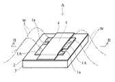
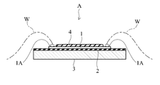
図1および図2は、本発明にかかるチップ抵抗器の一実施形態を示し、図3および図4は、その製造方法の一例を示している。図1および図2に示すように、本実施形態のチップ抵抗器Aは、抵抗体1、接着層2、基材3、および保護膜4を有して構成されている。このチップ抵抗器Aは、図示しないプリント配線板などにワイヤWを介して導通接続されるものであり、数十mΩ〜数百mΩ程度の低抵抗のものとして構成されている。
1 and 2 show an embodiment of a chip resistor according to the present invention, and FIGS. 3 and 4 show an example of a manufacturing method thereof. As shown in FIGS. 1 and 2, the chip resistor A of the present embodiment is configured to include a
抵抗体1は、温度抵抗係数(TCR)が比較的小さい、たとえばNi−Cr系合金、Ni−Cu系合金、Fe−Cr系合金、あるいはCu−Mn系合金といった金属板からなり、10〜100μm程度の厚みを有する。この抵抗体1は、所望とする抵抗値に調整すべくエッチングによって除去された切れ込み部1aを有する。切れ込み部1aが形成された両縁部1Aは、ワイヤWをボンディング接続するための電極パッド部として用いられる。
The
接着層2は、抵抗体1と基材3との間に設けられており、これら抵抗体1および基材3を強固に接合する役割を果たす。このような接着層2は、60〜100μm程度の厚みを有し、後述するように、たとえばガラス繊維に接着樹脂を含浸させたプリプレグ(絶縁性接着フィルム)からなる。
The
基材3は、プリント配線板などの実装面に直接固定されるものであり、抵抗体1の片面に接着層2を介して接合されている。この基材3は、たとえばアルミナあるいはガラスエポキシ樹脂といった絶縁性の材料からなり、チップ抵抗器Aの強度を高める役割を果たすとともに、通電時に抵抗体1に生じた熱を効率よく放散させるといった役割ももつ。このような基材3は、200〜400μm程度の厚みを有する。
The
保護膜4は、基材3の上から抵抗体1の中央部分を被覆して両縁部1Aを露出させるように設けられており、電気絶縁性をもつ例えばエポキシ樹脂系の絶縁材料を塗布することで形成されている。
The
次に、チップ抵抗器Aの製造方法の一例について、図3および図4を参照して説明する。 Next, an example of a manufacturing method of the chip resistor A will be described with reference to FIGS.
まず、図3(a)に示すように、抵抗体1の材料となる金属板10と、基材3となる絶縁性の基板30との間に、接着層2となるプリプレグ20を挟み込んだ状態とし、これら金属板10、プリプレグ20、および基板30を高圧真空プレスによって接合する。このような金属板10、プリプレグ20、および基板30は、チップ抵抗器Aを複数個取り可能なサイズを有し、抵抗体1、接着層2、および基材3それぞれの厚みに対応している。
First, as shown in FIG. 3A, a state in which a
次に、図3(b)に示すように、金属板10に対してエッチング処理を施すことにより、複数の抵抗体1を形成する。このようにして形成された抵抗体1は、両縁部1Aに切れ込み部1aを有する形態からなり、チップとなる各箇所に位置して互いに離間している。
Next, as shown in FIG. 3B, the plurality of
次に、図4(a)に示すように、抵抗体1の両縁部1Aを露出させて中央部分を覆うように基板10の上からストライプ状に絶縁膜40を塗布する。この絶縁膜40は、上述の保護膜4に相当するものである。その後、ハンダ付け性を良好にするなどといった必要があれば、抵抗体1の両縁部1Aには、Snなどのハンダ層(図示略)をメッキ処理によって形成するようにしてもよい。
Next, as shown in FIG. 4A, an
最後に、図4(b)に示すように、縦切断ラインL1および横切断ラインL2に沿って抵抗体1を囲うように切断することにより、抵抗体1、プリプレグ20、基板30、および絶縁膜40が一体となったものをチップ状に分割する。これにより、図1および図2に示すようなチップ抵抗器Aを複数個取りすることができる。
Finally, as shown in FIG. 4B, the
したがって、本実施形態のチップ抵抗器Aによれば、切れ込み部1aを有することで強度に乏しい抵抗体1であっても、下側の基材3に抵抗体1が支えられた状態でワイヤボンディング接続によって配線板などに実装されるので、チップ抵抗器A全体に十分な強度をもたせることができる。また、抵抗体1よりも大きい体積をもつ基材3によって放熱性を良好とすることができる。本実施形態のチップ抵抗器の製造方法によれば、上記した優れた効果をもつワイヤボンディング接続型のチップ抵抗器Aを容易に量産することができる。
Therefore, according to the chip resistor A of the present embodiment, even when the
本発明は、上述した実施形態の内容に限定されない。本発明にかかるチップ抵抗器の各部の具体的な構成は、種々に設計変更自在である。 The present invention is not limited to the contents of the above-described embodiment. The specific configuration of each part of the chip resistor according to the present invention can be varied in design in various ways.
1 抵抗体
1a 切れ込み部
1A 両縁部
2 接着層
3 基材
4 保護膜
10 金属板
20 プリプレグ
30 基板
40 絶縁膜
A チップ抵抗器
DESCRIPTION OF
Claims (5)
上記抵抗体全体を支持するように当該抵抗体の片面に接合された絶縁性の基材と、
上記抵抗体の両縁部をワイヤボンディング用の電極パッド部として露出させるように、上記基材の上から上記抵抗体の一部を被覆する保護膜と、
を備えていることを特徴とする、チップ抵抗器。 A chip resistor having a layered resistor,
An insulating base material joined to one side of the resistor so as to support the entire resistor;
A protective film covering a part of the resistor from above the base material so as to expose both edge portions of the resistor as electrode pads for wire bonding;
A chip resistor comprising: a chip resistor.
上記金属板にエッチングを施す工程と、
上記金属板の一部をワイヤボンディング用の電極パッド部として露出させてその余を覆うように、上記基板上に保護膜を形成する工程と、
上記金属板、上記基板、および上記保護膜が一体となったものをチップ状に分割する工程と、
を含むことを特徴とする、チップ抵抗器の製造方法。 Joining a metal plate as a material of the resistor and an insulating substrate as a base material;
Etching the metal plate; and
Forming a protective film on the substrate so as to expose a part of the metal plate as an electrode pad portion for wire bonding and cover the remainder;
Dividing the metal plate, the substrate, and the protective film into a single chip; and
A method of manufacturing a chip resistor, comprising:
Priority Applications (1)
| Application Number | Priority Date | Filing Date | Title |
|---|---|---|---|
| JP2008122203A JP2009272476A (en) | 2008-05-08 | 2008-05-08 | Chip resistor and method of manufacturing the same |
Applications Claiming Priority (1)
| Application Number | Priority Date | Filing Date | Title |
|---|---|---|---|
| JP2008122203A JP2009272476A (en) | 2008-05-08 | 2008-05-08 | Chip resistor and method of manufacturing the same |
Publications (1)
| Publication Number | Publication Date |
|---|---|
| JP2009272476A true JP2009272476A (en) | 2009-11-19 |
Family
ID=41438771
Family Applications (1)
| Application Number | Title | Priority Date | Filing Date |
|---|---|---|---|
| JP2008122203A Pending JP2009272476A (en) | 2008-05-08 | 2008-05-08 | Chip resistor and method of manufacturing the same |
Country Status (1)
| Country | Link |
|---|---|
| JP (1) | JP2009272476A (en) |
Cited By (3)
| Publication number | Priority date | Publication date | Assignee | Title |
|---|---|---|---|---|
| CN103594212A (en) * | 2012-08-17 | 2014-02-19 | 三星电机株式会社 | Chip resistor and method of manufacturing the same |
| CN107481825A (en) * | 2016-06-08 | 2017-12-15 | 兴亚株式会社 | Patch resistor |
| CN108520811A (en) * | 2018-03-14 | 2018-09-11 | 成都明杰科技有限公司 | A kind of precision resister reducing resistance varying-ratio |
-
2008
- 2008-05-08 JP JP2008122203A patent/JP2009272476A/en active Pending
Cited By (3)
| Publication number | Priority date | Publication date | Assignee | Title |
|---|---|---|---|---|
| CN103594212A (en) * | 2012-08-17 | 2014-02-19 | 三星电机株式会社 | Chip resistor and method of manufacturing the same |
| CN107481825A (en) * | 2016-06-08 | 2017-12-15 | 兴亚株式会社 | Patch resistor |
| CN108520811A (en) * | 2018-03-14 | 2018-09-11 | 成都明杰科技有限公司 | A kind of precision resister reducing resistance varying-ratio |
Similar Documents
| Publication | Publication Date | Title |
|---|---|---|
| JP2009302494A (en) | Chip resistor and method for manufacturing the same | |
| JP4632358B2 (en) | Chip type fuse | |
| JP5237299B2 (en) | Resistor (especially SMD resistor) and manufacturing method thereof | |
| JP5256544B2 (en) | Resistor | |
| JP4640952B2 (en) | Chip resistor and manufacturing method thereof | |
| WO2009005108A1 (en) | Resistor | |
| KR20150087429A (en) | Manufacturability of smd and through-hole fuses using laser process | |
| JP4257679B2 (en) | Electronic label and manufacturing method thereof | |
| US10102948B2 (en) | Chip resistor and method for making the same | |
| TW201306061A (en) | Micro-resistive device with soft material layer and manufacture method for the same | |
| US9514867B2 (en) | Chip resistor and method for making the same | |
| JP2009272476A (en) | Chip resistor and method of manufacturing the same | |
| JP2006310277A (en) | Chip type fuse | |
| US20180096758A1 (en) | Chip resistor and mounting structure thereof | |
| JP5464829B2 (en) | Chip resistor and manufacturing method thereof | |
| JP2014060463A (en) | Chip resistor and method for manufacturing the same | |
| JP2008270599A (en) | Metal plate resistor | |
| JP6732996B2 (en) | Chip resistor | |
| JP2008282904A (en) | Molded package, and manufacturing method thereof | |
| JPWO2017010216A1 (en) | Electronic components | |
| JP2000261123A (en) | Mounting structure of chip resistor and mounting method thereof | |
| JP2007141910A (en) | Resistor |