JP2009259934A - Solid-state imaging device - Google Patents
Solid-state imaging device Download PDFInfo
- Publication number
- JP2009259934A JP2009259934A JP2008105467A JP2008105467A JP2009259934A JP 2009259934 A JP2009259934 A JP 2009259934A JP 2008105467 A JP2008105467 A JP 2008105467A JP 2008105467 A JP2008105467 A JP 2008105467A JP 2009259934 A JP2009259934 A JP 2009259934A
- Authority
- JP
- Japan
- Prior art keywords
- solid
- film
- semiconductor substrate
- cut filter
- layer
- Prior art date
- Legal status (The legal status is an assumption and is not a legal conclusion. Google has not performed a legal analysis and makes no representation as to the accuracy of the status listed.)
- Pending
Links
Images


Abstract
Description
本発明は、固体撮像素子に関し、特に裏面照射型の固体撮像素子に関する。 The present invention relates to a solid-state image sensor, and more particularly to a back-illuminated solid-state image sensor.
固体撮像素子としては、CCD(Charge Coupled Device)型、CMOS(Complementary Metal-Oxide-Semiconductor)型が知られているが、近年、デジタルスチルカメラやカメラ付き携帯電話の小型化、低消費電力化に伴い、CMOS型の固体撮像素子が用いられることが多くなってきた。 As solid-state imaging devices, CCD (Charge Coupled Device) type and CMOS (Complementary Metal-Oxide-Semiconductor) type are known, but in recent years, digital still cameras and camera-equipped mobile phones have been reduced in size and power consumption. Along with this, CMOS type solid-state imaging devices are often used.
また、薄型化した半導体基板を使用し、その一方の面(受光面)側にフォトダイオードを含む受光部側要素を設け、この反対側の他方の面側に、外部との間で電気信号の入出力を行うための配線層を設けた構造の裏面照射型CMOSイメージセンサの提案、開発が行われている(例えば、特許文献1)。 Also, a thinned semiconductor substrate is used, and a light receiving unit side element including a photodiode is provided on one surface (light receiving surface) side, and an electric signal is transmitted to the outside on the other surface side on the opposite side. A backside illumination type CMOS image sensor having a structure in which a wiring layer for input / output is provided has been proposed and developed (for example, Patent Document 1).
しかし、裏面照射型の固体撮像素子は、受光面側からこの反対面側に形成された信号処理回路へと信号電荷を読み出して処理する必要性から、半導体基板の厚さを薄くする必要があり、赤外光などの長波長光が入射してきた場合には、容易に配線層側へと透過し、その配線層で反射した光が隣接画素のフォトダイオードに入射して混色を起こす可能性がある。
本発明は、光電変換素子に対する配線層側からの赤外光の入射を防止した固体撮像素子を提供する。 The present invention provides a solid-state imaging device that prevents the incidence of infrared light from the wiring layer side to the photoelectric conversion device.
本発明の一態様によれば、一方の面に受光面を有する半導体基板と、前記半導体基板の他方の面上に設けられた配線層と、前記受光面と前記配線層との間に設けられた撮像画素部と、前記撮像画素部の周辺であって前記半導体基板の前記他方の面側に設けられた周辺回路部と、を備え、前記撮像画素部は、2次元アレイ状に配列された複数の光電変換素子と、前記光電変換素子を画素ごとに区切る素子分離層と、少なくとも、前記光電変換素子と前記配線層との間に部分的に設けられた赤外線カットフィルタ膜もしくは遮光膜と、を有することを特徴とする固体撮像素子が提供される。 According to one aspect of the present invention, a semiconductor substrate having a light receiving surface on one surface, a wiring layer provided on the other surface of the semiconductor substrate, and provided between the light receiving surface and the wiring layer. An imaging pixel unit, and a peripheral circuit unit provided around the imaging pixel unit and on the other surface side of the semiconductor substrate, and the imaging pixel unit is arranged in a two-dimensional array A plurality of photoelectric conversion elements, an element isolation layer that divides the photoelectric conversion elements for each pixel, and at least an infrared cut filter film or a light shielding film provided partially between the photoelectric conversion elements and the wiring layer, A solid-state imaging device is provided.
本発明によれば、光電変換素子に対する配線層側からの赤外光の入射を防止した固体撮像素子が提供される。 ADVANTAGE OF THE INVENTION According to this invention, the solid-state image sensor which prevented incidence | injection of the infrared light from the wiring layer side with respect to a photoelectric conversion element is provided.
以下、図面を参照し、本発明の実施形態について説明する。 Hereinafter, embodiments of the present invention will be described with reference to the drawings.
本発明の実施形態に係る固体撮像素子は、厚さが例えば10μm以下の薄い半導体基板にフォトダイオード、各種トランジスタなどが形成され、さらにこれらの上に多層配線構造部が設けられた構造を有し、その半導体基板の裏面(多層配線構造部が設けられた面の反対側の面)側から入射する光をフォトダイオードに受けるいわゆる裏面照射型の固体撮像素子である。また、本実施形態では、固体撮像素子としてCMOSイメージセンサを例に挙げて説明する。 The solid-state imaging device according to the embodiment of the present invention has a structure in which a photodiode, various transistors, and the like are formed on a thin semiconductor substrate having a thickness of, for example, 10 μm or less, and a multilayer wiring structure portion is provided thereon. This is a so-called back-illuminated solid-state imaging device in which light incident from the back surface (surface opposite to the surface provided with the multilayer wiring structure portion) of the semiconductor substrate is received by a photodiode. In the present embodiment, a CMOS image sensor will be described as an example of the solid-state imaging device.
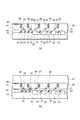
図1は、本発明の実施形態に係る固体撮像素子における撮像画素部(センサ部)11と周辺回路部12〜18の平面レイアウトを示す模式図である。
FIG. 1 is a schematic diagram illustrating a planar layout of an imaging pixel unit (sensor unit) 11 and
1つの半導体チップ(半導体基板)10に、撮像画素部11と周辺回路部12〜18が設けられている。
An
撮像画素部11は、2次元アレイ状に配列された多数の光電変換素子としての例えばフォトダイオードを有する。1つの光電変換素子が1画素に対応する。
The
周辺回路部は、撮像画素部11から出力される電気信号(画素信号)を処理する信号処理回路と、撮像画素部11の各画素を駆動して画素信号の出力を制御する駆動制御回路とを有する。
The peripheral circuit unit includes a signal processing circuit that processes an electrical signal (pixel signal) output from the
各画素は、垂直選択手段12によって、垂直方向に水平ライン(行)単位で順次選択され、タイミングジェネレータ13からの各種パルス信号によって各画素のトランジスタが制御されることにより、各画素の信号が相関二重サンプリング回路14に読み出される。
Each pixel is sequentially selected in units of horizontal lines (rows) in the vertical direction by the vertical selection means 12, and the transistors of each pixel are controlled by various pulse signals from the
相関二重サンプリング回路14は、画素信号に対して相関二重サンプリング等の信号処理を行う。水平選択手段15は、相関二重サンプリング回路14の出力信号をゲインコントロール回路18に出力し、その出力信号に対してゲインコントロール回路18は所定のゲインコントロールを行う。A/D変換回路17は、ゲインコントロール回路18の出力信号をアナログからデジタルに変換する。デジタルアンプ16は、A/D変換回路17のデジタル信号出力に対して増幅やバッファリングなどを行う。
The correlated
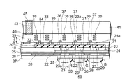
図2は、本発明の実施形態に係る固体撮像素子の要部断面構造を示す模式図である。 FIG. 2 is a schematic diagram illustrating a cross-sectional structure of a main part of the solid-state imaging device according to the embodiment of the present invention.
P型の半導体基板(例えばシリコン基板)10において、撮像画素部11に対応する領域には、P+型の素子分離層22によって各画素ごとに区切られて(分離されて)、2次元アレイ状に配列された複数のN型拡散層23が形成されている。
In a P-type semiconductor substrate (for example, a silicon substrate) 10, a region corresponding to the
N型拡散層23及び素子分離層22における一方の面側にはP+型の表面層24が形成されている。N型拡散層23とP+型表面層24とはPN接合しており、これらは光電変換素子としてのフォトダイオード30を構成する。
A P + -
また、半導体基板10において、P+型表面層24が形成された一方の面側が受光面50として機能し、この受光面50側には、カラーフィルタR、G、Bやマイクロレンズ29などが設けられている。
Further, in the
受光面50には、例えばシリコン酸化膜等の絶縁膜25が形成され、その絶縁膜25には、例えばアルミニウム等の遮光膜28が形成されている。遮光膜28は、半導体基板10の一方の面(受光面50)側全体にわたって存在するが全面を遮蔽しておらず、N型拡散層23に対向する部分、および後述する位置合わせマーク31に対向する部分は開口されている。
An
絶縁膜25には、遮光膜28を覆うように、例えばシリコン窒化膜等のパッシベーション膜26が形成されている。パッシベーション膜26上には、N型拡散層23の位置に対応して、赤、緑、青の各カラーフィルタR、G、Bが形成され、またカラーフィルタR、G、Bを覆うように平坦化層(例えば有機膜)27が形成されている。平坦化層27には、各カラーフィルターR、G、Bに対応する位置にマイクロレンズ29が設けられている。
A
半導体基板10において、受光面50の反対側の他方の面上には、P型半導体層20、多層配線構造部、支持基板41が設けられている。
In the
P型半導体層20において、撮像画素部11に対応する領域には、フォトダイオード30で光電変換された電荷が転送され蓄積されるFD(Floating Diffusion)部36が選択的に形成されている。FD部36は、N型拡散層23に対して少し横にずれた位置に形成されている。FD部36の上方であって、N型拡散層23側にずれた位置には、ゲート絶縁膜を介して転送ゲート37が設けられている。
In the P-
N型拡散層23とP型半導体層20との間には選択的に赤外線カットフィルタ膜(もしくは遮光膜)21が設けられている。赤外線カットフィルタ膜(もしくは遮光膜)21は、P型半導体層20側から見てN型拡散層23を遮蔽する位置に設けられているが、N型拡散層23のすべてを遮蔽しておらず、N型拡散層23においてFD部36側の一部はP型半導体層20に接している。この部分を介して、光電変換によりN型拡散層23中に発生した電荷を、FD部36に転送することができる。
An infrared cut filter film (or a light shielding film) 21 is selectively provided between the N-
赤外線カットフィルタ膜(もしくは遮光膜)21は、少なくとも約700nm以上の波長の赤外光を透過させない特性を有し、且つ電気絶縁性も有する。
図3に、赤外線カットフィルタ膜21の具体的構成例を示す。
The infrared cut filter film (or light-shielding film) 21 has characteristics that do not transmit infrared light having a wavelength of at least about 700 nm or more, and also has electrical insulation.
FIG. 3 shows a specific configuration example of the infrared
赤外線カットフィルタ膜21は、屈折率の異なる(屈折率に高低の差がある)2種類の誘電体膜を交互に繰り返し積層した構造を有する。半導体基板10側の1層目には、λ/2(λは赤外光の波長)の厚さで高屈折率膜51が形成されている。その上の2層目にはλ/4の厚さで低屈折率膜52が形成され、その上の3層目にはλ/4の厚さで高屈折率膜51が形成されている。以降、2層目と3層目とを交互に繰り返した積層構造が形成され、最上層にはλ/2の厚さで高屈折率膜51が形成されている。高屈折率膜51の材料としては、例えばTiO2(屈折率n=2.4〜2.5)、ZrO(屈折率n=2.4)を挙げることができる。低屈折率膜52の材料としては、例えばSiO2(屈折率n=1.46)を挙げることができる。
また、赤外光だけでなく可視光に対する遮光性も有する遮光膜21を用いてもよい。この遮光膜としては、例えば、窒化チタン、酸化クロム、シリカ、アルミナのうち少なくともいずれかを含む材料を用いることができる。
The infrared
Further, a
再び図2を参照すると、P型半導体層20において、撮像画素部領域より外側の周辺回路部に対応する領域には、各種トランジスタ35のソース、ドレインとして機能するN型拡散領域32、33が形成されている。これらN型拡散領域32、33間の上にはゲート絶縁膜を介してゲート電極34が設けられている。
Referring to FIG. 2 again, in the P-
これらトランジスタ35が形成された部分と半導体基板10との間には、赤外線カットフィルタ膜(もしくは遮光膜)21が設けられている。赤外線カットフィルタ膜(もしくは遮光膜)21は、半導体基板10の裏面(受光面50)側から見て、トランジスタ35が形成された周辺回路部を遮蔽している。
An infrared cut filter film (or a light shielding film) 21 is provided between the portion where the
P型半導体層20において、周辺回路部よりさらに外側には、例えばアルミニウム等の金属膜からなる位置合わせマーク31が形成されている。この位置合わせマーク31は、図1に示すように、例えばライン状に形成されている。
In the P-
P型半導体層20の上には、複数層の配線層38と層間絶縁膜39とを有する多層配線構造部が設けられている。この多層配線構造部の上には、支持基板41が設けられている。層間絶縁膜39の表面側には、配線層38と接続された電極パッド40が形成されている。支持基板41の表面上において電極パッド40に対向する位置には電極端子45が形成されている。電極パッド40と電極端子45とは、支持基板41を貫通して設けられた導電材43を介して接続されている。
On the P-
以上説明したように構成される本実施形態に係る固体撮像素子は裏面照射型であり、半導体基板10の裏面(受光面50)側から光が入射する。この入射光は、マイクロレンズ29で集光され、各カラーフィルターR、G、Bを通過して、フォトダイオード30に入射する。
The solid-state imaging device according to this embodiment configured as described above is a backside illumination type, and light enters from the backside (light receiving surface 50) side of the
フォトダイオード30に入射した光は光電変換され、これにより発生した電荷は、転送トランジスタによってFD部36に転送・蓄積され、このFD部36の電位変動が増幅トランジスタによって検出され、周辺回路部に出力される。
Light incident on the
ここで、図10は、比較例の固体撮像素子を示す。この比較例の固体撮像素子は、赤外線カットフィルタ膜(もしくは遮光膜)21を有さない点で、前述した本実施形態に係る固体撮像素子と異なる。 Here, FIG. 10 shows a solid-state imaging device of a comparative example. The solid-state image sensor of this comparative example is different from the solid-state image sensor according to this embodiment described above in that it does not have the infrared cut filter film (or light-shielding film) 21.
裏面照射型の固体撮像素子は、受光面側からこの反対面側に形成された信号処理回路へと信号電荷を読み出して処理する必要性から、一般に半導体基板の厚さは10μm以下と薄くする必要があり、赤外光などの長波長光が入射してきた場合には、図10の比較例において1点鎖線の光路で示すように、容易に配線層38側へと透過し、配線層38で反射した光が隣接画素のフォトダイオード30に入射して混色を起こす可能性がある。
In the back-illuminated solid-state imaging device, the thickness of the semiconductor substrate is generally required to be as thin as 10 μm or less because it is necessary to read and process signal charges from the light receiving surface side to the signal processing circuit formed on the opposite surface side. When long wavelength light such as infrared light is incident, it is easily transmitted to the
これに対して、本実施形態では、フォトダイオード30と配線層38との間に赤外線カットフィルタ膜(もしくは遮光膜)21を設けているため、受光面50から素子分離層22を透過して配線層38に到達した長波長光(赤外光)が配線層38で反射しても、その反射光は赤外線カットフィルタ膜(もしくは遮光膜)21によってフォトダイオード30への入射が阻まれるため、混色を起こすことがない。
On the other hand, in this embodiment, since the infrared cut filter film (or light shielding film) 21 is provided between the
次に、図4〜図7を参照して、本実施形態に係る固体撮像素子の製造方法の一例について説明する。 Next, an example of a method for manufacturing the solid-state imaging device according to the present embodiment will be described with reference to FIGS.
まず、図4(a)に示すように、P型シリコンの半導体基板10上に、選択的に赤外線カットフィルタ膜(もしくは遮光膜)21を形成する。赤外線カットフィルタ膜(もしくは遮光膜)21は、例えば図3を参照して前述したような構造を有する。赤外線カットフィルタ膜(もしくは遮光膜)21は、まず半導体基板10上全面に形成された後、選択的エッチングにより、所望の部分が開口される。
First, as shown in FIG. 4A, an infrared cut filter film (or a light shielding film) 21 is selectively formed on a P-type
次に、赤外線カットフィルタ膜(もしくは遮光膜)21の開口に露出している半導体基板10表面部分を結晶の成長種として、図4(b)に示すように、P型半導体層20を、選択エピタキシャル横方向成長(ELO:Epitaxial Lateral Overgrowth)させる。赤外線カットフィルタ膜(もしくは遮光膜)21としては、このエピタキシャル成長プロセスにおける温度に耐えうる材料とする必要がある。
Next, using the surface portion of the
P型半導体層20は、赤外線カットフィルタ膜(もしくは遮光膜)21上にも成長し、赤外線カットフィルタ膜(もしくは遮光膜)21上の中央付近で、開口側から成長してきた結晶が結合する。この結合部20aは結晶性が悪く欠陥が集中する部分であるので、後工程にてP型半導体層20に形成するFD部、ソース、ドレインとなるN型拡散領域などは結晶成長結合部20aを避けた部分に形成する。
The P-
P型半導体層20の表面を、例えばCMP(Chemical Mechanical Polishing)法により平らに研磨した後、撮像画素領域については、N型拡散層23、P+型の素子分離層22、FD部36、転送ゲート37、信号増幅トランジスタなどを形成し、周辺回路部については、信号処理トランジスタなどを形成する。N型拡散層23、素子分離層22、FD部36、N型拡散領域32、33は、P型半導体層20側からの各種不純物のイオン注入により形成することができる。
After the surface of the P-
また、これら要素の形成と併せて、P型半導体層20における、周辺回路部よりも外側の表層部に、例えばアルミニウム等の金属パターンとして、位置合わせマーク31を形成する。この位置合わせマーク31は、後工程で半導体基板10の裏面(受光面)側の要素を形成する際に、表面側に形成された要素との位置合わせを行うために用いられる。
In addition to the formation of these elements, the
次に、図5(a)に示すように、P型半導体層20の上に、多層配線層38と層間絶縁膜(例えばシリコン酸化層)39とを有する多層配線構造部を形成する。さらに、層間絶縁膜39の表面に、配線層38と接続された電極パッド40も形成する。
Next, as shown in FIG. 5A, a multilayer wiring structure having a
多層配線構造部の表面を平坦化した後、その上に、図5(b)に示すように、支持基板41を貼り付ける。支持基板41は、半導体基板10の薄型化のために裏面側を研磨する際の支持体としての機能を担う。
After the surface of the multilayer wiring structure is flattened, a
次に、半導体基板10の裏面側をN型拡散層23が露出するまで研磨して半導体基板10を薄型化し、その後、裏面側から位置合わせマーク31に赤外線を照射して位置合わせマーク31を検知して位置合わせを行いつつ、図6(a)に示すように、撮像画素領域における素子分離層22及びN型拡散層23の裏面側に、例えばボロンをイオン注入してP+型表面層24を形成する。位置合わせマーク31に対向する部分には赤外線カットフィルタ膜(もしくは遮光膜)21は形成されていないため、半導体基板10裏面側からの赤外線照射により位置合わせマーク31の検出が可能となっている。
Next, the back surface side of the
次に、半導体基板10の裏面を保護膜で覆った上で、図6(b)に示すように、支持基板41に電極パッド40まで達する貫通ビア42を形成し、その後、図7(a)に示すように、貫通ビア42内に導電材43を埋め込み、支持基板41表面における導電材43上に電極端子45を形成する。
Next, after covering the back surface of the
次に、半導体基板10裏面側に形成した保護膜を除去し、今度は支持基板41表面を保護膜で覆った上で、図7(b)に示すように、半導体基板10裏面側に、絶縁膜(例えばシリコン酸化膜)25、遮光膜(例えばアルミニウム等の金属膜)28、パッシベーション膜(例えばシリコン窒化膜)26を形成する。
Next, the protective film formed on the back surface side of the
この後、図2に示すカラーフィルタR、G、B、平坦化層27、マイクロレンズ29などを受光面側に形成し、さらにウェーハ状態から各チップごとに分割して、本実施形態に係る固体撮像素子(CMOSイメージセンサチップ)が得られる。
Thereafter, the color filters R, G, and B, the
図8は、本発明の他の実施形態に係る固体撮像素子の要部断面構造を示す模式図である。なお、図2に示す前述した固体撮像素子と同じ要素には同じ符号を付しその詳細な説明は省略する。 FIG. 8 is a schematic diagram showing a cross-sectional structure of a main part of a solid-state imaging device according to another embodiment of the present invention. The same elements as those of the above-described solid-state imaging device shown in FIG. 2 are denoted by the same reference numerals, and detailed description thereof is omitted.
この図8に示す固体撮像素子においては、素子分離層22とP型半導体層20との間にも赤外線カットフィルタ膜(もしくは遮光膜)21を設けている。撮像画素部領域においては、赤外線カットフィルタ膜(もしくは遮光膜)21は、N型拡散層23の一部23aを除く全面にわたって形成されている。この一部23aは、光電変換によりN型拡散層23に発生した電荷を、転送ゲート37の動作によりFD36へと転送するための経路である。
In the solid-state imaging device shown in FIG. 8, an infrared cut filter film (or light shielding film) 21 is also provided between the
この図8に示す構造によれば、素子分離層22と配線層38との間にも赤外線カットフィルタ膜(もしくは遮光膜)21があるので、受光面50側から入射して素子分離層22を透過する長波長光(赤外光)の配線層38側への入射を阻むことができる。すなわち、受光面50側から入射する赤外光が配線層38へと到達することがなく、よってその配線層38での反射光がフォトダイオード30に入射することによる混色も生じない。
According to the structure shown in FIG. 8, since there is an infrared cut filter film (or light shielding film) 21 between the
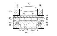
次に、図9は、図2や図8を参照して前述した本発明の実施形態に係る固体撮像素子(図9中では符号60で示す)を用いたカメラモジュールの模式図を示す。
Next, FIG. 9 shows a schematic diagram of a camera module using the solid-state imaging device (indicated by
固体撮像素子60の電極端子45と回路基板70との間には導電性バンプ67が設けられ、そのバンプ67を介して、固体撮像素子60は回路基板70に対して電気的に接続されて実装されている。固体撮像素子60と回路基板70との接合部には、樹脂スペーサ65が設けられている。
固体撮像素子60の受光面は光学的レンズ61と、空間を隔てて対向している。光学的レンズ61は、例えば円筒状のレンズホルダ62に保持されている。レンズホルダ62と固体撮像素子60との間には樹脂スペーサ64が設けられている。また、このカメラモジュールにおいて、光学的レンズ61を除く他の要素の外面にはメタルシールド63が形成されている。
The light receiving surface of the solid-
近年、カメラ付き携帯電話の薄型化が進み、WLCM(Wafer Level Camera Module)構造による低背型カメラモジュールが開発されている。しかし、この構造の場合、カメラモジュールの裏面側の隙間より赤外光が入射し、半導体基板10において受光面と反対側の面側に形成された配線層パターンが撮像されてしまうといった問題がある。
2. Description of the Related Art In recent years, camera-type mobile phones have been made thinner, and low-profile camera modules having a WLCM (Wafer Level Camera Module) structure have been developed. However, in the case of this structure, there is a problem that infrared light is incident from the gap on the back side of the camera module, and the wiring layer pattern formed on the surface of the
しかし、本実施形態によれば、図2または図8を参照して前述したように、受光面の反対側から赤外光が漏れて入射してきたとしても、赤外線カットフィルタ膜(もしくは遮光膜)21によって、その赤外光のフォトダイオード30への入射が阻まれ、配線層38が撮像されてしまうことがない。
However, according to the present embodiment, as described above with reference to FIG. 2 or FIG. 8, even if infrared light leaks and enters from the opposite side of the light receiving surface, the infrared cut filter film (or light shielding film) 21 prevents the infrared light from entering the
また、周辺回路部にも赤外線カットフィルタ膜(もしくは遮光膜)21を設けていることで、周辺回路部の裏面(受光面の反対側の面)側から漏れ込んできた赤外光が、直接周辺回路部のトランジスタに入射したり、あるいは金属膜である遮光膜28にまで到達して反射し、その反射光が隣接するトランジスタや撮像画素領域のフォトダイオード30や配線層38へ到達して入射するのを防ぐことができる。
Further, since the infrared cut filter film (or the light shielding film) 21 is also provided in the peripheral circuit portion, the infrared light leaked from the back surface (surface opposite to the light receiving surface) side of the peripheral circuit portion is directly The light enters the transistor in the peripheral circuit section, or reaches the
ここで、図11は比較例のカメラモジュールを示す。なお、図9に対応する要素にはお同じ符号を付している。本実施形態のような赤外線カットフィルタ膜(もしくは遮光膜)21を設けていない固体撮像素子80を用いる場合、この図11に示すように、固体撮像素子80の受光面と光学的レンズ61との間にフィルム状の赤外線カットフィルタ71を組み込むことが考えられる。
Here, FIG. 11 shows a camera module of a comparative example. In addition, the same code | symbol is attached | subjected to the element corresponding to FIG. When using the solid-
しかし、この場合、カメラモジュールの一部品として赤外線カットフィルタ71を組み込むため、半導体基板に薄膜として赤外線カットフィルタ膜21を形成する本発明実施形態に比べてモジュール全体の高さは大きくなり低背化に不利であり、さらに部品点数の増加による組み立て工程の工数増加をまねく。また、図11の構造では、受光面の反対面側から漏れて入射してくる赤外光による配線パターンの撮像を防ぐことはできない。
However, in this case, since the
以上、具体例を参照しつつ本発明の実施形態について説明した。しかし、本発明は、それらに限定されるものではなく、本発明の技術的思想に基づいて種々の変形が可能である。 The embodiments of the present invention have been described above with reference to specific examples. However, the present invention is not limited to them, and various modifications can be made based on the technical idea of the present invention.
N型拡散層23、素子分離層22を形成するにあたっては、半導体基板10を支持基板41に貼り付けた後、半導体基板10の受光面側を研磨して薄型化し、この後、その受光面側からのイオン注入により、N型拡散層23、素子分離層22を形成してもよい。
In forming the N-
10…半導体基板、11…撮像画素部、20…P型半導体層、21…赤外線カットフィルタ膜(もしくは遮光膜)、22…素子分離層、23…N型拡散層、24…P+型表面層、30…光電変換素子(フォトダイオード)、31…位置合わせマーク、36…FD(Floating Diffusion)部、37…転送ゲート、38…配線層、41…支持基板、50…受光面
DESCRIPTION OF
Claims (5)
前記半導体基板の他方の面上に設けられた配線層と、
前記受光面と前記配線層との間に設けられた撮像画素部と、
前記撮像画素部の周辺であって前記半導体基板の前記他方の面側に設けられた周辺回路部と、
を備え、
前記撮像画素部は、
2次元アレイ状に配列された複数の光電変換素子と、
前記光電変換素子を画素ごとに区切る素子分離層と、
少なくとも、前記光電変換素子と前記配線層との間に部分的に設けられた赤外線カットフィルタ膜もしくは遮光膜と、
を有することを特徴とする固体撮像素子。 A semiconductor substrate having a light receiving surface on one side;
A wiring layer provided on the other surface of the semiconductor substrate;
An imaging pixel portion provided between the light receiving surface and the wiring layer;
A peripheral circuit portion provided around the imaging pixel portion and on the other surface side of the semiconductor substrate;
With
The imaging pixel unit includes:
A plurality of photoelectric conversion elements arranged in a two-dimensional array;
An element isolation layer that divides the photoelectric conversion element for each pixel;
At least an infrared cut filter film or a light shielding film partially provided between the photoelectric conversion element and the wiring layer;
A solid-state imaging device comprising:
前記受光面と前記位置合わせマークとの間には前記赤外線カットフィルタ膜もしくは遮光膜は設けられず、赤外線を使って前記受光面側から前記位置合わせマークを読み取り可能であることを特徴とする請求項1〜3のいずれか1つに記載の固体撮像素子。 An alignment mark is formed outside the peripheral circuit portion,
The infrared cut filter film or the light shielding film is not provided between the light receiving surface and the alignment mark, and the alignment mark can be read from the light receiving surface side using infrared rays. Item 4. The solid-state imaging device according to any one of Items 1 to 3.
Priority Applications (1)
| Application Number | Priority Date | Filing Date | Title |
|---|---|---|---|
| JP2008105467A JP2009259934A (en) | 2008-04-15 | 2008-04-15 | Solid-state imaging device |
Applications Claiming Priority (1)
| Application Number | Priority Date | Filing Date | Title |
|---|---|---|---|
| JP2008105467A JP2009259934A (en) | 2008-04-15 | 2008-04-15 | Solid-state imaging device |
Publications (1)
| Publication Number | Publication Date |
|---|---|
| JP2009259934A true JP2009259934A (en) | 2009-11-05 |
Family
ID=41387014
Family Applications (1)
| Application Number | Title | Priority Date | Filing Date |
|---|---|---|---|
| JP2008105467A Pending JP2009259934A (en) | 2008-04-15 | 2008-04-15 | Solid-state imaging device |
Country Status (1)
| Country | Link |
|---|---|
| JP (1) | JP2009259934A (en) |
Cited By (10)
| Publication number | Priority date | Publication date | Assignee | Title |
|---|---|---|---|---|
| WO2010131534A1 (en) * | 2009-05-12 | 2010-11-18 | Canon Kabushiki Kaisha | Solid-state image sensing apparatus |
| CN102315234A (en) * | 2010-07-06 | 2012-01-11 | 索尼公司 | Solid photographic device and manufacturing approach thereof, solid camera head and camera head |
| JP2012231032A (en) * | 2011-04-26 | 2012-11-22 | Canon Inc | Solid state imaging device and imaging apparatus |
| US8711263B2 (en) | 2010-11-12 | 2014-04-29 | Sony Corporation | Solid-state imaging device and electronic apparatus with antireflection structure |
| US8835981B2 (en) | 2012-06-29 | 2014-09-16 | Kabushiki Kaisha Toshiba | Solid-state image sensor |
| JP2016149515A (en) * | 2015-02-12 | 2016-08-18 | オプティツ インコーポレイテッド | Rear surface illumination type image sensor including non-planner light interface |
| JP2017208397A (en) * | 2016-05-17 | 2017-11-24 | リコーイメージング株式会社 | Backside irradiation type solid-state imaging element and imaging apparatus |
| CN109906512A (en) * | 2016-10-27 | 2019-06-18 | 索尼半导体解决方案公司 | Photographing element and electronic equipment |
| JP2020074465A (en) * | 2010-07-01 | 2020-05-14 | 株式会社半導体エネルギー研究所 | Image sensor |
| WO2021090545A1 (en) * | 2019-11-08 | 2021-05-14 | ソニーセミコンダクタソリューションズ株式会社 | Imaging element and imaging device |
-
2008
- 2008-04-15 JP JP2008105467A patent/JP2009259934A/en active Pending
Cited By (15)
| Publication number | Priority date | Publication date | Assignee | Title |
|---|---|---|---|---|
| US8319305B2 (en) | 2009-05-12 | 2012-11-27 | Canon Kabushiki Kaisha | Solid-state image sensing apparatus |
| WO2010131534A1 (en) * | 2009-05-12 | 2010-11-18 | Canon Kabushiki Kaisha | Solid-state image sensing apparatus |
| JP2020074465A (en) * | 2010-07-01 | 2020-05-14 | 株式会社半導体エネルギー研究所 | Image sensor |
| CN102315234A (en) * | 2010-07-06 | 2012-01-11 | 索尼公司 | Solid photographic device and manufacturing approach thereof, solid camera head and camera head |
| US8760545B2 (en) | 2010-07-06 | 2014-06-24 | Sony Corporation | Solid-state imaging device, manufacturing method therefor, solid-state imaging apparatus, and image capturing apparatus |
| US9472589B2 (en) | 2010-11-12 | 2016-10-18 | Sony Corporation | Solid-state imaging device and electronic apparatus |
| US8711263B2 (en) | 2010-11-12 | 2014-04-29 | Sony Corporation | Solid-state imaging device and electronic apparatus with antireflection structure |
| JP2012231032A (en) * | 2011-04-26 | 2012-11-22 | Canon Inc | Solid state imaging device and imaging apparatus |
| US8835981B2 (en) | 2012-06-29 | 2014-09-16 | Kabushiki Kaisha Toshiba | Solid-state image sensor |
| US10139619B2 (en) | 2015-02-12 | 2018-11-27 | Optiz, Inc. | Back side illumination image sensor with non-planar optical interface |
| JP2016149515A (en) * | 2015-02-12 | 2016-08-18 | オプティツ インコーポレイテッド | Rear surface illumination type image sensor including non-planner light interface |
| JP2017208397A (en) * | 2016-05-17 | 2017-11-24 | リコーイメージング株式会社 | Backside irradiation type solid-state imaging element and imaging apparatus |
| CN109906512A (en) * | 2016-10-27 | 2019-06-18 | 索尼半导体解决方案公司 | Photographing element and electronic equipment |
| CN109906512B (en) * | 2016-10-27 | 2023-08-15 | 索尼半导体解决方案公司 | Image pickup element and electronic apparatus |
| WO2021090545A1 (en) * | 2019-11-08 | 2021-05-14 | ソニーセミコンダクタソリューションズ株式会社 | Imaging element and imaging device |
Similar Documents
| Publication | Publication Date | Title |
|---|---|---|
| US11217620B2 (en) | Solid-state image sensor for phase difference detection, method of manufacturing the same, and electronic device | |
| KR101893325B1 (en) | Solid-state imaging device, method of manufacturing the same, and electronic apparatus | |
| KR101574878B1 (en) | Solid-state imaging device and method for manufacturing solid-state imaging device | |
| US9349766B2 (en) | Solid-state imaging device | |
| JP4621719B2 (en) | Back-illuminated image sensor | |
| JP2009259934A (en) | Solid-state imaging device | |
| KR101944115B1 (en) | Solid-state imaging device, manufacturing method of the same and electronic apparatus | |
| US9064767B2 (en) | Solid state imaging device and method of manufacturing the same | |
| JP2010040621A (en) | Solid-state imaging device, and method of manufacturing the same | |
| JP2012169530A (en) | Solid state image sensor, manufacturing method therefor, and electronic apparatus | |
| KR20120001895A (en) | An image sensor and package comprising the same | |
| WO2008065952A1 (en) | Solid-state imaging device, its manufacturing method, and electronic information device | |
| JP2010161321A (en) | Optical device and method of manufacturing the same | |
| KR102622057B1 (en) | Image sensor | |
| TW200832688A (en) | Solid-state image capturing apparatus and electronic information device | |
| US20120104523A1 (en) | Solid-state imaging device manufacturing method of solid-state imaging device, and electronic apparatus | |
| KR20150015350A (en) | Method of manufacturing solid-state imaging device and solid-state imaging device | |
| JP2015082510A (en) | Solid-state imaging element, method of manufacturing the same, and electronic device | |
| JP2008172005A (en) | Solid-state image pickup device, electronic module and electronic device | |
| JP2016082103A (en) | Solid state image pickup device and manufacturing method of solid state image pickup device | |
| JP2011238636A (en) | Solid-state imaging device and manufacturing method therefor |