JP2009238708A - Manufacturing method for organic electroluminescent apparatus - Google Patents
Manufacturing method for organic electroluminescent apparatus Download PDFInfo
- Publication number
- JP2009238708A JP2009238708A JP2008086877A JP2008086877A JP2009238708A JP 2009238708 A JP2009238708 A JP 2009238708A JP 2008086877 A JP2008086877 A JP 2008086877A JP 2008086877 A JP2008086877 A JP 2008086877A JP 2009238708 A JP2009238708 A JP 2009238708A
- Authority
- JP
- Japan
- Prior art keywords
- ink
- layer
- pixel region
- organic
- manufacturing
- Prior art date
- Legal status (The legal status is an assumption and is not a legal conclusion. Google has not performed a legal analysis and makes no representation as to the accuracy of the status listed.)
- Pending
Links
- 238000004519 manufacturing process Methods 0.000 title claims abstract description 50
- 238000000034 method Methods 0.000 claims abstract description 56
- 238000005192 partition Methods 0.000 claims abstract description 36
- 238000001035 drying Methods 0.000 claims abstract description 33
- 150000002894 organic compounds Chemical class 0.000 claims abstract description 8
- 239000002904 solvent Substances 0.000 claims description 41
- 238000005401 electroluminescence Methods 0.000 claims description 38
- 239000000463 material Substances 0.000 claims description 35
- 238000000576 coating method Methods 0.000 claims description 22
- 238000007639 printing Methods 0.000 claims description 17
- 239000011248 coating agent Substances 0.000 claims description 13
- LYCAIKOWRPUZTN-UHFFFAOYSA-N Ethylene glycol Chemical compound OCCO LYCAIKOWRPUZTN-UHFFFAOYSA-N 0.000 claims description 11
- XLYOFNOQVPJJNP-UHFFFAOYSA-N water Substances O XLYOFNOQVPJJNP-UHFFFAOYSA-N 0.000 claims description 11
- 238000010030 laminating Methods 0.000 claims description 5
- ZAMOUSCENKQFHK-UHFFFAOYSA-N Chlorine atom Chemical compound [Cl] ZAMOUSCENKQFHK-UHFFFAOYSA-N 0.000 claims description 4
- RTZKZFJDLAIYFH-UHFFFAOYSA-N Diethyl ether Chemical compound CCOCC RTZKZFJDLAIYFH-UHFFFAOYSA-N 0.000 claims description 4
- LFQSCWFLJHTTHZ-UHFFFAOYSA-N Ethanol Chemical compound CCO LFQSCWFLJHTTHZ-UHFFFAOYSA-N 0.000 claims description 4
- 150000004945 aromatic hydrocarbons Chemical class 0.000 claims description 4
- 239000000460 chlorine Substances 0.000 claims description 4
- 229910052801 chlorine Inorganic materials 0.000 claims description 4
- WGCNASOHLSPBMP-UHFFFAOYSA-N hydroxyacetaldehyde Natural products OCC=O WGCNASOHLSPBMP-UHFFFAOYSA-N 0.000 claims description 4
- 239000002861 polymer material Substances 0.000 claims description 4
- 229920001940 conductive polymer Polymers 0.000 claims description 3
- JBTWLSYIZRCDFO-UHFFFAOYSA-N ethyl methyl carbonate Chemical compound CCOC(=O)OC JBTWLSYIZRCDFO-UHFFFAOYSA-N 0.000 claims description 2
- 230000008569 process Effects 0.000 abstract description 8
- 239000010410 layer Substances 0.000 description 207
- 239000000976 ink Substances 0.000 description 151
- 238000002347 injection Methods 0.000 description 41
- 239000007924 injection Substances 0.000 description 41
- 230000004048 modification Effects 0.000 description 20
- 238000012986 modification Methods 0.000 description 20
- 230000005525 hole transport Effects 0.000 description 19
- 239000011159 matrix material Substances 0.000 description 18
- 239000000758 substrate Substances 0.000 description 16
- 239000010408 film Substances 0.000 description 11
- 229910052751 metal Inorganic materials 0.000 description 11
- 239000002184 metal Substances 0.000 description 11
- -1 ITO Chemical compound 0.000 description 9
- 230000015572 biosynthetic process Effects 0.000 description 9
- 229920001609 Poly(3,4-ethylenedioxythiophene) Polymers 0.000 description 7
- 239000000243 solution Substances 0.000 description 7
- 239000002019 doping agent Substances 0.000 description 5
- 239000010409 thin film Substances 0.000 description 5
- 230000000903 blocking effect Effects 0.000 description 4
- 239000003086 colorant Substances 0.000 description 4
- 150000004696 coordination complex Chemical class 0.000 description 4
- 230000007547 defect Effects 0.000 description 4
- 239000000975 dye Substances 0.000 description 4
- 150000004866 oxadiazoles Chemical class 0.000 description 4
- 239000005871 repellent Substances 0.000 description 4
- YMWUJEATGCHHMB-UHFFFAOYSA-N Dichloromethane Chemical compound ClCCl YMWUJEATGCHHMB-UHFFFAOYSA-N 0.000 description 3
- XEKOWRVHYACXOJ-UHFFFAOYSA-N Ethyl acetate Chemical compound CCOC(C)=O XEKOWRVHYACXOJ-UHFFFAOYSA-N 0.000 description 3
- OKKJLVBELUTLKV-UHFFFAOYSA-N Methanol Chemical compound OC OKKJLVBELUTLKV-UHFFFAOYSA-N 0.000 description 3
- DNIAPMSPPWPWGF-UHFFFAOYSA-N Propylene glycol Chemical compound CC(O)CO DNIAPMSPPWPWGF-UHFFFAOYSA-N 0.000 description 3
- YXFVVABEGXRONW-UHFFFAOYSA-N Toluene Chemical compound CC1=CC=CC=C1 YXFVVABEGXRONW-UHFFFAOYSA-N 0.000 description 3
- 230000000052 comparative effect Effects 0.000 description 3
- 238000011109 contamination Methods 0.000 description 3
- RAXXELZNTBOGNW-UHFFFAOYSA-N imidazole Natural products C1=CNC=N1 RAXXELZNTBOGNW-UHFFFAOYSA-N 0.000 description 3
- 239000007788 liquid Substances 0.000 description 3
- 229920000123 polythiophene Polymers 0.000 description 3
- 229910052725 zinc Inorganic materials 0.000 description 3
- 239000011701 zinc Substances 0.000 description 3
- FYGHSUNMUKGBRK-UHFFFAOYSA-N 1,2,3-trimethylbenzene Chemical compound CC1=CC=CC(C)=C1C FYGHSUNMUKGBRK-UHFFFAOYSA-N 0.000 description 2
- VQGHOUODWALEFC-UHFFFAOYSA-N 2-phenylpyridine Chemical compound C1=CC=CC=C1C1=CC=CC=N1 VQGHOUODWALEFC-UHFFFAOYSA-N 0.000 description 2
- HEDRZPFGACZZDS-UHFFFAOYSA-N Chloroform Chemical compound ClC(Cl)Cl HEDRZPFGACZZDS-UHFFFAOYSA-N 0.000 description 2
- 229910052693 Europium Inorganic materials 0.000 description 2
- KFZMGEQAYNKOFK-UHFFFAOYSA-N Isopropanol Chemical compound CC(C)O KFZMGEQAYNKOFK-UHFFFAOYSA-N 0.000 description 2
- LRHPLDYGYMQRHN-UHFFFAOYSA-N N-Butanol Chemical compound CCCCO LRHPLDYGYMQRHN-UHFFFAOYSA-N 0.000 description 2
- HCHKCACWOHOZIP-UHFFFAOYSA-N Zinc Chemical compound [Zn] HCHKCACWOHOZIP-UHFFFAOYSA-N 0.000 description 2
- XLOMVQKBTHCTTD-UHFFFAOYSA-N Zinc monoxide Chemical compound [Zn]=O XLOMVQKBTHCTTD-UHFFFAOYSA-N 0.000 description 2
- 239000005456 alcohol based solvent Substances 0.000 description 2
- 229910052783 alkali metal Inorganic materials 0.000 description 2
- 150000001340 alkali metals Chemical class 0.000 description 2
- 229910052784 alkaline earth metal Inorganic materials 0.000 description 2
- 150000001342 alkaline earth metals Chemical class 0.000 description 2
- 239000000956 alloy Substances 0.000 description 2
- 229910045601 alloy Inorganic materials 0.000 description 2
- 229910052782 aluminium Inorganic materials 0.000 description 2
- 150000001412 amines Chemical class 0.000 description 2
- RDOXTESZEPMUJZ-UHFFFAOYSA-N anisole Chemical compound COC1=CC=CC=C1 RDOXTESZEPMUJZ-UHFFFAOYSA-N 0.000 description 2
- MVPPADPHJFYWMZ-UHFFFAOYSA-N chlorobenzene Chemical compound ClC1=CC=CC=C1 MVPPADPHJFYWMZ-UHFFFAOYSA-N 0.000 description 2
- 239000011365 complex material Substances 0.000 description 2
- 150000001875 compounds Chemical class 0.000 description 2
- 238000009429 electrical wiring Methods 0.000 description 2
- 239000003759 ester based solvent Substances 0.000 description 2
- 239000004210 ether based solvent Substances 0.000 description 2
- 239000004973 liquid crystal related substance Substances 0.000 description 2
- 238000005259 measurement Methods 0.000 description 2
- 239000000203 mixture Substances 0.000 description 2
- 239000012044 organic layer Substances 0.000 description 2
- 238000002559 palpation Methods 0.000 description 2
- 125000002080 perylenyl group Chemical group C1(=CC=C2C=CC=C3C4=CC=CC5=CC=CC(C1=C23)=C45)* 0.000 description 2
- 238000009832 plasma treatment Methods 0.000 description 2
- BASFCYQUMIYNBI-UHFFFAOYSA-N platinum Chemical compound [Pt] BASFCYQUMIYNBI-UHFFFAOYSA-N 0.000 description 2
- 229920003227 poly(N-vinyl carbazole) Polymers 0.000 description 2
- 229920000548 poly(silane) polymer Polymers 0.000 description 2
- 229920000767 polyaniline Polymers 0.000 description 2
- 229920002098 polyfluorene Polymers 0.000 description 2
- UOHMMEJUHBCKEE-UHFFFAOYSA-N prehnitene Chemical compound CC1=CC=C(C)C(C)=C1C UOHMMEJUHBCKEE-UHFFFAOYSA-N 0.000 description 2
- 150000003219 pyrazolines Chemical class 0.000 description 2
- 230000002940 repellent Effects 0.000 description 2
- 239000000126 substance Substances 0.000 description 2
- 230000000007 visual effect Effects 0.000 description 2
- NGQSLSMAEVWNPU-YTEMWHBBSA-N 1,2-bis[(e)-2-phenylethenyl]benzene Chemical class C=1C=CC=CC=1/C=C/C1=CC=CC=C1\C=C\C1=CC=CC=C1 NGQSLSMAEVWNPU-YTEMWHBBSA-N 0.000 description 1
- SHXCHSNZIGEBFL-UHFFFAOYSA-N 1,3-benzothiazole;zinc Chemical class [Zn].C1=CC=C2SC=NC2=C1 SHXCHSNZIGEBFL-UHFFFAOYSA-N 0.000 description 1
- AZQWKYJCGOJGHM-UHFFFAOYSA-N 1,4-benzoquinone Chemical compound O=C1C=CC(=O)C=C1 AZQWKYJCGOJGHM-UHFFFAOYSA-N 0.000 description 1
- VFBJMPNFKOMEEW-UHFFFAOYSA-N 2,3-diphenylbut-2-enedinitrile Chemical group C=1C=CC=CC=1C(C#N)=C(C#N)C1=CC=CC=C1 VFBJMPNFKOMEEW-UHFFFAOYSA-N 0.000 description 1
- OGGKVJMNFFSDEV-UHFFFAOYSA-N 3-methyl-n-[4-[4-(n-(3-methylphenyl)anilino)phenyl]phenyl]-n-phenylaniline Chemical group CC1=CC=CC(N(C=2C=CC=CC=2)C=2C=CC(=CC=2)C=2C=CC(=CC=2)N(C=2C=CC=CC=2)C=2C=C(C)C=CC=2)=C1 OGGKVJMNFFSDEV-UHFFFAOYSA-N 0.000 description 1
- DDTHMESPCBONDT-UHFFFAOYSA-N 4-(4-oxocyclohexa-2,5-dien-1-ylidene)cyclohexa-2,5-dien-1-one Chemical class C1=CC(=O)C=CC1=C1C=CC(=O)C=C1 DDTHMESPCBONDT-UHFFFAOYSA-N 0.000 description 1
- 239000005725 8-Hydroxyquinoline Substances 0.000 description 1
- PAYRUJLWNCNPSJ-UHFFFAOYSA-N Aniline Chemical compound NC1=CC=CC=C1 PAYRUJLWNCNPSJ-UHFFFAOYSA-N 0.000 description 1
- DKPFZGUDAPQIHT-UHFFFAOYSA-N Butyl acetate Natural products CCCCOC(C)=O DKPFZGUDAPQIHT-UHFFFAOYSA-N 0.000 description 1
- AJWRRBADQOOFSF-UHFFFAOYSA-N C1=CC=C2OC([Zn])=NC2=C1 Chemical class C1=CC=C2OC([Zn])=NC2=C1 AJWRRBADQOOFSF-UHFFFAOYSA-N 0.000 description 1
- UXYHZIYEDDINQH-UHFFFAOYSA-N C1=CNC2=C3C=NN=C3C=CC2=C1 Chemical class C1=CNC2=C3C=NN=C3C=CC2=C1 UXYHZIYEDDINQH-UHFFFAOYSA-N 0.000 description 1
- BVKZGUZCCUSVTD-UHFFFAOYSA-L Carbonate Chemical compound [O-]C([O-])=O BVKZGUZCCUSVTD-UHFFFAOYSA-L 0.000 description 1
- RYGMFSIKBFXOCR-UHFFFAOYSA-N Copper Chemical compound [Cu] RYGMFSIKBFXOCR-UHFFFAOYSA-N 0.000 description 1
- 229930192627 Naphthoquinone Natural products 0.000 description 1
- CTQNGGLPUBDAKN-UHFFFAOYSA-N O-Xylene Chemical compound CC1=CC=CC=C1C CTQNGGLPUBDAKN-UHFFFAOYSA-N 0.000 description 1
- 229920000265 Polyparaphenylene Polymers 0.000 description 1
- 229920000292 Polyquinoline Polymers 0.000 description 1
- JUJWROOIHBZHMG-UHFFFAOYSA-N Pyridine Chemical group C1=CC=NC=C1 JUJWROOIHBZHMG-UHFFFAOYSA-N 0.000 description 1
- NRCMAYZCPIVABH-UHFFFAOYSA-N Quinacridone Chemical class N1C2=CC=CC=C2C(=O)C2=C1C=C1C(=O)C3=CC=CC=C3NC1=C2 NRCMAYZCPIVABH-UHFFFAOYSA-N 0.000 description 1
- XUIMIQQOPSSXEZ-UHFFFAOYSA-N Silicon Chemical compound [Si] XUIMIQQOPSSXEZ-UHFFFAOYSA-N 0.000 description 1
- BQCADISMDOOEFD-UHFFFAOYSA-N Silver Chemical compound [Ag] BQCADISMDOOEFD-UHFFFAOYSA-N 0.000 description 1
- 229910052771 Terbium Inorganic materials 0.000 description 1
- YTPLMLYBLZKORZ-UHFFFAOYSA-N Thiophene Chemical group C=1C=CSC=1 YTPLMLYBLZKORZ-UHFFFAOYSA-N 0.000 description 1
- XHCLAFWTIXFWPH-UHFFFAOYSA-N [O-2].[O-2].[O-2].[O-2].[O-2].[V+5].[V+5] Chemical compound [O-2].[O-2].[O-2].[O-2].[O-2].[V+5].[V+5] XHCLAFWTIXFWPH-UHFFFAOYSA-N 0.000 description 1
- 230000002411 adverse Effects 0.000 description 1
- HSFWRNGVRCDJHI-UHFFFAOYSA-N alpha-acetylene Natural products C#C HSFWRNGVRCDJHI-UHFFFAOYSA-N 0.000 description 1
- XAGFODPZIPBFFR-UHFFFAOYSA-N aluminium Chemical compound [Al] XAGFODPZIPBFFR-UHFFFAOYSA-N 0.000 description 1
- 125000003277 amino group Chemical group 0.000 description 1
- 229910003481 amorphous carbon Inorganic materials 0.000 description 1
- 150000004056 anthraquinones Chemical class 0.000 description 1
- 239000007864 aqueous solution Substances 0.000 description 1
- 150000004982 aromatic amines Chemical class 0.000 description 1
- 125000003118 aryl group Chemical group 0.000 description 1
- QVGXLLKOCUKJST-UHFFFAOYSA-N atomic oxygen Chemical compound [O] QVGXLLKOCUKJST-UHFFFAOYSA-N 0.000 description 1
- 230000004888 barrier function Effects 0.000 description 1
- 230000008901 benefit Effects 0.000 description 1
- 229910052790 beryllium Inorganic materials 0.000 description 1
- 125000000609 carbazolyl group Chemical class C1(=CC=CC=2C3=CC=CC=C3NC12)* 0.000 description 1
- 239000010406 cathode material Substances 0.000 description 1
- 230000008859 change Effects 0.000 description 1
- 238000006243 chemical reaction Methods 0.000 description 1
- 239000006103 coloring component Substances 0.000 description 1
- 229910052802 copper Inorganic materials 0.000 description 1
- 239000010949 copper Substances 0.000 description 1
- 150000001893 coumarin derivatives Chemical class 0.000 description 1
- HFXKQSZZZPGLKQ-UHFFFAOYSA-N cyclopentamine Chemical class CNC(C)CC1CCCC1 HFXKQSZZZPGLKQ-UHFFFAOYSA-N 0.000 description 1
- CUIWZLHUNCCYBL-UHFFFAOYSA-N decacyclene Chemical compound C12=C([C]34)C=CC=C4C=CC=C3C2=C2C(=C34)C=C[CH]C4=CC=CC3=C2C2=C1C1=CC=CC3=CC=CC2=C31 CUIWZLHUNCCYBL-UHFFFAOYSA-N 0.000 description 1
- 230000002950 deficient Effects 0.000 description 1
- 238000010586 diagram Methods 0.000 description 1
- 238000007599 discharging Methods 0.000 description 1
- 230000000694 effects Effects 0.000 description 1
- OGPBJKLSAFTDLK-UHFFFAOYSA-N europium atom Chemical compound [Eu] OGPBJKLSAFTDLK-UHFFFAOYSA-N 0.000 description 1
- 230000005281 excited state Effects 0.000 description 1
- 150000008376 fluorenones Chemical class 0.000 description 1
- JVZRCNQLWOELDU-UHFFFAOYSA-N gamma-Phenylpyridine Natural products C1=CC=CC=C1C1=CC=NC=C1 JVZRCNQLWOELDU-UHFFFAOYSA-N 0.000 description 1
- 239000011521 glass Substances 0.000 description 1
- PCHJSUWPFVWCPO-UHFFFAOYSA-N gold Chemical compound [Au] PCHJSUWPFVWCPO-UHFFFAOYSA-N 0.000 description 1
- 229910052737 gold Inorganic materials 0.000 description 1
- 239000010931 gold Substances 0.000 description 1
- 150000004820 halides Chemical class 0.000 description 1
- FUZZWVXGSFPDMH-UHFFFAOYSA-M hexanoate Chemical compound CCCCCC([O-])=O FUZZWVXGSFPDMH-UHFFFAOYSA-M 0.000 description 1
- 229940083761 high-ceiling diuretics pyrazolone derivative Drugs 0.000 description 1
- 150000007857 hydrazones Chemical class 0.000 description 1
- 238000005286 illumination Methods 0.000 description 1
- 150000002460 imidazoles Chemical class 0.000 description 1
- 229910003437 indium oxide Inorganic materials 0.000 description 1
- PJXISJQVUVHSOJ-UHFFFAOYSA-N indium(iii) oxide Chemical compound [O-2].[O-2].[O-2].[In+3].[In+3] PJXISJQVUVHSOJ-UHFFFAOYSA-N 0.000 description 1
- 238000007641 inkjet printing Methods 0.000 description 1
- 238000009434 installation Methods 0.000 description 1
- 229940079865 intestinal antiinfectives imidazole derivative Drugs 0.000 description 1
- 150000002503 iridium Chemical class 0.000 description 1
- 239000002648 laminated material Substances 0.000 description 1
- 239000003446 ligand Substances 0.000 description 1
- 238000004020 luminiscence type Methods 0.000 description 1
- 229910044991 metal oxide Inorganic materials 0.000 description 1
- 150000004706 metal oxides Chemical class 0.000 description 1
- 229910052976 metal sulfide Inorganic materials 0.000 description 1
- 150000002739 metals Chemical class 0.000 description 1
- UZKWTJUDCOPSNM-UHFFFAOYSA-N methoxybenzene Substances CCCCOC=C UZKWTJUDCOPSNM-UHFFFAOYSA-N 0.000 description 1
- 229910000476 molybdenum oxide Inorganic materials 0.000 description 1
- DCZNSJVFOQPSRV-UHFFFAOYSA-N n,n-diphenyl-4-[4-(n-phenylanilino)phenyl]aniline Chemical class C1=CC=CC=C1N(C=1C=CC(=CC=1)C=1C=CC(=CC=1)N(C=1C=CC=CC=1)C=1C=CC=CC=1)C1=CC=CC=C1 DCZNSJVFOQPSRV-UHFFFAOYSA-N 0.000 description 1
- IBHBKWKFFTZAHE-UHFFFAOYSA-N n-[4-[4-(n-naphthalen-1-ylanilino)phenyl]phenyl]-n-phenylnaphthalen-1-amine Chemical group C1=CC=CC=C1N(C=1C2=CC=CC=C2C=CC=1)C1=CC=C(C=2C=CC(=CC=2)N(C=2C=CC=CC=2)C=2C3=CC=CC=C3C=CC=2)C=C1 IBHBKWKFFTZAHE-UHFFFAOYSA-N 0.000 description 1
- 150000002791 naphthoquinones Chemical class 0.000 description 1
- QGLKJKCYBOYXKC-UHFFFAOYSA-N nonaoxidotritungsten Chemical compound O=[W]1(=O)O[W](=O)(=O)O[W](=O)(=O)O1 QGLKJKCYBOYXKC-UHFFFAOYSA-N 0.000 description 1
- 239000011368 organic material Substances 0.000 description 1
- WCPAKWJPBJAGKN-UHFFFAOYSA-N oxadiazole Chemical compound C1=CON=N1 WCPAKWJPBJAGKN-UHFFFAOYSA-N 0.000 description 1
- TWNQGVIAIRXVLR-UHFFFAOYSA-N oxo(oxoalumanyloxy)alumane Chemical compound O=[Al]O[Al]=O TWNQGVIAIRXVLR-UHFFFAOYSA-N 0.000 description 1
- PQQKPALAQIIWST-UHFFFAOYSA-N oxomolybdenum Chemical compound [Mo]=O PQQKPALAQIIWST-UHFFFAOYSA-N 0.000 description 1
- 229910052760 oxygen Inorganic materials 0.000 description 1
- 239000001301 oxygen Substances 0.000 description 1
- BPUBBGLMJRNUCC-UHFFFAOYSA-N oxygen(2-);tantalum(5+) Chemical compound [O-2].[O-2].[O-2].[O-2].[O-2].[Ta+5].[Ta+5] BPUBBGLMJRNUCC-UHFFFAOYSA-N 0.000 description 1
- 229960003540 oxyquinoline Drugs 0.000 description 1
- NRNFFDZCBYOZJY-UHFFFAOYSA-N p-quinodimethane Chemical compound C=C1C=CC(=C)C=C1 NRNFFDZCBYOZJY-UHFFFAOYSA-N 0.000 description 1
- 239000002245 particle Substances 0.000 description 1
- DGBWPZSGHAXYGK-UHFFFAOYSA-N perinone Chemical class C12=NC3=CC=CC=C3N2C(=O)C2=CC=C3C4=C2C1=CC=C4C(=O)N1C2=CC=CC=C2N=C13 DGBWPZSGHAXYGK-UHFFFAOYSA-N 0.000 description 1
- FIZIRKROSLGMPL-UHFFFAOYSA-N phenoxazin-1-one Chemical compound C1=CC=C2N=C3C(=O)C=CC=C3OC2=C1 FIZIRKROSLGMPL-UHFFFAOYSA-N 0.000 description 1
- UOMHBFAJZRZNQD-UHFFFAOYSA-N phenoxazone Natural products C1=CC=C2OC3=CC(=O)C=CC3=NC2=C1 UOMHBFAJZRZNQD-UHFFFAOYSA-N 0.000 description 1
- IEQIEDJGQAUEQZ-UHFFFAOYSA-N phthalocyanine Chemical compound N1C(N=C2C3=CC=CC=C3C(N=C3C4=CC=CC=C4C(=N4)N3)=N2)=C(C=CC=C2)C2=C1N=C1C2=CC=CC=C2C4=N1 IEQIEDJGQAUEQZ-UHFFFAOYSA-N 0.000 description 1
- 239000000049 pigment Substances 0.000 description 1
- 229920003023 plastic Polymers 0.000 description 1
- 239000004033 plastic Substances 0.000 description 1
- 150000003057 platinum Chemical class 0.000 description 1
- 229910052697 platinum Inorganic materials 0.000 description 1
- 229920000553 poly(phenylenevinylene) Polymers 0.000 description 1
- 229920000172 poly(styrenesulfonic acid) Polymers 0.000 description 1
- 229920001197 polyacetylene Polymers 0.000 description 1
- 229920000642 polymer Polymers 0.000 description 1
- 229920006254 polymer film Polymers 0.000 description 1
- 229920000128 polypyrrole Polymers 0.000 description 1
- 229920001296 polysiloxane Polymers 0.000 description 1
- 229940005642 polystyrene sulfonic acid Drugs 0.000 description 1
- 150000004033 porphyrin derivatives Chemical class 0.000 description 1
- 150000004032 porphyrins Chemical class 0.000 description 1
- 230000001737 promoting effect Effects 0.000 description 1
- BDERNNFJNOPAEC-UHFFFAOYSA-N propan-1-ol Chemical compound CCCO BDERNNFJNOPAEC-UHFFFAOYSA-N 0.000 description 1
- JEXVQSWXXUJEMA-UHFFFAOYSA-N pyrazol-3-one Chemical class O=C1C=CN=N1 JEXVQSWXXUJEMA-UHFFFAOYSA-N 0.000 description 1
- 150000003233 pyrroles Chemical class 0.000 description 1
- MCJGNVYPOGVAJF-UHFFFAOYSA-N quinolin-8-ol Chemical compound C1=CN=C2C(O)=CC=CC2=C1 MCJGNVYPOGVAJF-UHFFFAOYSA-N 0.000 description 1
- 125000002943 quinolinyl group Chemical group N1=C(C=CC2=CC=CC=C12)* 0.000 description 1
- 229910052761 rare earth metal Inorganic materials 0.000 description 1
- 150000002910 rare earth metals Chemical class 0.000 description 1
- YYMBJDOZVAITBP-UHFFFAOYSA-N rubrene Chemical class C1=CC=CC=C1C(C1=C(C=2C=CC=CC=2)C2=CC=CC=C2C(C=2C=CC=CC=2)=C11)=C(C=CC=C2)C2=C1C1=CC=CC=C1 YYMBJDOZVAITBP-UHFFFAOYSA-N 0.000 description 1
- 229910001925 ruthenium oxide Inorganic materials 0.000 description 1
- WOCIAKWEIIZHES-UHFFFAOYSA-N ruthenium(iv) oxide Chemical compound O=[Ru]=O WOCIAKWEIIZHES-UHFFFAOYSA-N 0.000 description 1
- 239000010703 silicon Substances 0.000 description 1
- 229910052710 silicon Inorganic materials 0.000 description 1
- 229910052709 silver Inorganic materials 0.000 description 1
- 239000004332 silver Substances 0.000 description 1
- 238000004528 spin coating Methods 0.000 description 1
- 230000007480 spreading Effects 0.000 description 1
- 238000003892 spreading Methods 0.000 description 1
- PJANXHGTPQOBST-UHFFFAOYSA-N stilbene Chemical class C=1C=CC=CC=1C=CC1=CC=CC=C1 PJANXHGTPQOBST-UHFFFAOYSA-N 0.000 description 1
- 125000005504 styryl group Chemical group 0.000 description 1
- 239000000725 suspension Substances 0.000 description 1
- 229940042055 systemic antimycotics triazole derivative Drugs 0.000 description 1
- 229910001936 tantalum oxide Inorganic materials 0.000 description 1
- 150000003518 tetracenes Chemical class 0.000 description 1
- VLLMWSRANPNYQX-UHFFFAOYSA-N thiadiazole Chemical compound C1=CSN=N1.C1=CSN=N1 VLLMWSRANPNYQX-UHFFFAOYSA-N 0.000 description 1
- XOLBLPGZBRYERU-UHFFFAOYSA-N tin dioxide Chemical compound O=[Sn]=O XOLBLPGZBRYERU-UHFFFAOYSA-N 0.000 description 1
- 229910001887 tin oxide Inorganic materials 0.000 description 1
- 229910052723 transition metal Inorganic materials 0.000 description 1
- 150000003624 transition metals Chemical class 0.000 description 1
- 238000002834 transmittance Methods 0.000 description 1
- 150000001651 triphenylamine derivatives Chemical class 0.000 description 1
- 229910001930 tungsten oxide Inorganic materials 0.000 description 1
- 238000001771 vacuum deposition Methods 0.000 description 1
- 229910001935 vanadium oxide Inorganic materials 0.000 description 1
- 239000008096 xylene Substances 0.000 description 1
- YVTHLONGBIQYBO-UHFFFAOYSA-N zinc indium(3+) oxygen(2-) Chemical compound [O--].[Zn++].[In+3] YVTHLONGBIQYBO-UHFFFAOYSA-N 0.000 description 1
- 239000011787 zinc oxide Substances 0.000 description 1
Images


Landscapes
- Electroluminescent Light Sources (AREA)
Abstract
Description
本発明は、有機エレクトロルミネッセンス装置(以下、本明細書において「有機EL装置」ということがある)の製造方法に関し、詳しくは、陽極と陰極と有機化合物を含む発光層を備える有機エレクトロルミネッセンス素子(以下、本明細書において「有機EL素子」ということがある)を複数備える有機EL装置の製造方法に関する。 The present invention relates to a method for manufacturing an organic electroluminescence device (hereinafter, also referred to as “organic EL device” in the present specification), and more specifically, an organic electroluminescence element (hereinafter, referred to as an organic electroluminescence device) including a light emitting layer including an anode, a cathode, and an organic compound. Hereinafter, the present invention relates to a method for manufacturing an organic EL device including a plurality of organic EL devices.
有機EL素子およびこれを搭載した有機EL装置は、より高い性能の装置を開発するべく、様々な検討がなされている。有機EL素子は、一般に、陽極、陰極およびこれらに挟まれた発光層を有する。発光層は電圧が印加されて発光する有機化合物で形成される。有機EL素子は様々な特性を有するが、薄膜を積層して形成できるため、これを実装する表示装置などの装置を極めて薄型にし得る点が一つの大きな特徴となっている。 Various studies have been made on organic EL elements and organic EL devices equipped with the organic EL elements in order to develop higher performance devices. The organic EL element generally has an anode, a cathode, and a light emitting layer sandwiched between them. The light emitting layer is formed of an organic compound that emits light when voltage is applied. An organic EL element has various characteristics, but since it can be formed by laminating thin films, one major feature is that a device such as a display device on which the organic EL element is mounted can be made extremely thin.
有機EL素子は、通常、支持基板上に、電極を構成する層および発光層を所定の順序で積層させて作製される。有機EL素子を構成する各層は、各層を構成する成分や要求される厚さ等の条件に応じて、様々な方法が採用され得る。層形成方法の一つの態様としては、溶液中に層を構成する成分を混合してその溶液を塗布し、これを乾燥等により硬化させて層を形成させることができる。溶液を塗布する方法としては、例えば、スピンコート法などのコート法(薄膜形成法)、およびフレキソ印刷法、インクジェットプリント法などの印刷法などが挙げられる。 An organic EL element is usually produced by laminating a layer constituting an electrode and a light emitting layer in a predetermined order on a support substrate. Various methods can be employed for each layer constituting the organic EL element depending on conditions such as components constituting each layer and required thickness. As one aspect of the layer forming method, the components constituting the layer are mixed in the solution, the solution is applied, and the solution is cured by drying or the like to form the layer. Examples of the method for applying the solution include a coating method (thin film forming method) such as a spin coating method, and a printing method such as a flexographic printing method and an inkjet printing method.
中でもインクジェット法は、数ミクロン単位での制御が可能であること、色素材料の塗布量を最低限に抑制できること、色の三原色ごとの塗布が容易であり、フルカラーの表示装置を作製しやすいことなどの利点があり、有機EL素子およびこれを搭載する有機EL装置の製造方法として様々な方法が研究、開発されている(例えば、特許文献1など)。 In particular, the inkjet method can be controlled in units of several microns, the coating amount of the pigment material can be minimized, the coating of each of the three primary colors is easy, and a full-color display device can be easily manufactured. Various methods have been researched and developed as a method for manufacturing an organic EL element and an organic EL device equipped with the organic EL element (for example, Patent Document 1).
インクジェット法は、インクの粒子または小滴を噴射ノズルから吐出させて、被印刷体上にインクを付着させる方法である。インクジェット法では、インクを噴射することから、そのインクは、フレキソ印刷などで用いられるインクに比べて相当に粘度が低い溶液が用いられる。被印刷体上に付着したインクは、自然乾燥等によりインク中の溶媒が留去されて、インク中に溶媒として含まれていた発色成分が被印刷体上に固定される。したがって、インクジェット法などのように粘度の低い溶液を塗布するタイプの層形成方法(または成膜方法)においては、インクが被体に付着した後、乾燥するという工程が含まれる。 The ink-jet method is a method in which ink particles or small droplets are ejected from ejection nozzles to adhere ink onto a printing medium. In the ink jet method, since ink is ejected, a solution having a considerably lower viscosity than the ink used in flexographic printing or the like is used as the ink. As for the ink adhered on the printing medium, the solvent in the ink is distilled off by natural drying or the like, and the coloring component contained as a solvent in the ink is fixed on the printing medium. Therefore, a layer forming method (or a film forming method) of applying a solution having a low viscosity, such as an ink jet method, includes a step of drying after the ink adheres to the object.
有機EL素子を作製する過程でも、インクジェット法などの方法を採用する場合は、上記と同様にインクの塗布工程と、塗布後のインクを乾燥する工程が含まれる。しかしながら、インクジェットなどの塗布手法を用いて有機EL素子を作製する場合に、インクの塗布、乾燥後にインクが画素領域内全体に十分広がりきらないという問題が生じる場合があった。インクが画素領域十分に広がりきらない場合、本来直接接触すべきではない層同士が接触し、電流リークを生じる可能性がある。また、層の厚みにむらが生じた場合、そのインクで構成される層は本来予定される機能を十分に発揮しきれず、有機EL素子の発光不良、耐久性不足などをまねく可能性もある。 Even in the process of manufacturing the organic EL element, when a method such as an ink jet method is employed, an ink application step and a step of drying the applied ink are included as described above. However, when an organic EL element is manufactured using a coating method such as ink jet, there is a problem that the ink cannot be sufficiently spread over the entire pixel region after the ink is applied and dried. If the ink does not spread sufficiently in the pixel area, layers that should not be in direct contact with each other may come into contact with each other, resulting in current leakage. In addition, when the thickness of the layer becomes uneven, the layer composed of the ink cannot fully perform the originally planned function, and there is a possibility that the organic EL element may not emit light or the durability is insufficient.
本発明は、上記課題を解決し、簡便に、歩留まり良く有機EL装置を製造する方法を提供することを課題とする。 An object of the present invention is to solve the above-described problems and to provide a method for manufacturing an organic EL device simply and with high yield.
本発明者らは鋭意研究を進めたところ、上記のような課題は、画素の平面形状が矩形または楕円形のごとく、長辺または長軸を有する図形形状において、それらの長手方向の両端に生じやすい傾向があるという知見を得た。さらに研究を進め、表面張力の高いインクを用いる場合に生じやすい傾向があるという知見も得た。これらの知見に基づき、上記のような課題は、インクジェット法などの方法により画素領域内に点状に塗布されたインクが、塗布後に画素領域内で表面張力により中心方向に収縮し、その結果長手方向の両端部にインクが被膜されなくなってしまうということが一つの原因として推定された。そこで、上記課題を解決すべく、本発明は下記の構成を採用するものである。 As a result of intensive research, the present inventors have found that the above-described problems occur at both ends in the longitudinal direction of a graphic shape having a long side or a long axis such as a rectangular shape or an elliptical shape of a pixel. The knowledge that it tends to be easy was acquired. Further research has been conducted, and it has been found that there is a tendency to occur when ink having a high surface tension is used. Based on these findings, the above-mentioned problem is that the ink applied in a dot-like manner in the pixel area by a method such as an ink jet method shrinks in the center direction due to surface tension in the pixel area after application, and as a result, It was estimated as one cause that the ink was not coated on both ends in the direction. In order to solve the above problems, the present invention adopts the following configuration.
〔1〕複数の画素を有し、前記画素が少なくとも一対の電極と当該電極間に挟まれた有機化合物を含む発光層を含む積層体で形成される有機エレクトロルミネッセンス素子で構成される有機エレクトロルミネッセンス装置の製造方法であって、
前記画素が形成される画素領域は、当該領域を囲む隔壁により区画され、長辺または長軸を有する平面形状を有し、
前記有機エレクトロルミネッセンス素子が、前記積層体を構成する層を前記画素領域内に順次積層して形成され、前記積層体を構成する層のうちの少なくとも一層を形成する工程は、塗布工程と乾燥工程とを含み、
前記塗布工程において、前記層を形成する成分とインク溶媒とを含むインクを非断続的に連続して吐出し、前記画素領域および当該画素領域の長手方向にある隔壁上に非断続的に連続して前記インクを塗布しながら、前記画素領域の長手方向に並ぶ複数の画素領域上に線状に前記インクを塗布し、
前記乾燥工程において、塗布された前記インクを乾燥する、
有機エレクトロルミネッセンス装置の製造方法。
〔2〕前記画素領域の平面形状が、矩形状または楕円形状である、上記〔1〕に記載の有機エレクトロルミネッセンス装置の製造方法。
〔3〕前記隔壁の表面の全部、または、前記画素領域の長手方向に面する隔壁表面が、撥水性を有する、上記〔1〕または〔2〕に記載の有機エレクトロルミネッセンス装置の製造方法。
〔4〕前記層を形成する成分が、導電性高分子材料を含む、上記〔1〕から〔3〕のいずれか一項に記載の有機エレクトロルミネッセンス装置の製造方法。
〔5〕前記層を形成する成分が、発光材料を含む、上記〔1〕から〔4〕のいずれか一項に記載の有機エレクトロルミネッセンス装置の製造方法。
〔6〕前記インク溶媒が、水、アルコール溶媒、グリコール溶媒、エーテル溶媒、エステル溶媒、含塩素溶媒および芳香族炭化水素溶媒からなる群より選ばれる少なくとも1つを含む、上記〔1〕から〔5〕のいずれか一項に記載の有機エレクトロルミネッセンス装置の製造方法。
〔7〕前記塗布工程において、吐出されるインクの粘度が3cP以上、13cP以下である、上記〔1〕から〔6〕のいずれか一項に記載の有機エレクトロルミネッセンス装置の製造方法。
〔8〕前記塗布する工程において、ノズルプリンティング装置を用いて、非断続的に連続してインクを吐出する、上記〔1〕から〔7〕のいずれか一項に記載の有機エレクトロルミネッセンス装置の製造方法。
〔9〕前記乾燥する工程において、20℃以上、90℃以下の温度条件下の空気中で、インクを乾燥させる、上記〔1〕から〔8〕のいずれか一項に記載の有機エレクトロルミネッセンス装置の製造方法。
〔10〕前記有機エレクトロルミネッセンス装置は、複数の画素が画素領域の長手方向に一列に配置され、当該列が画素領域の短手方向に複数連接されてなる表示エリア部を備えており、
前記塗布工程においては、前記画素領域の長手方向の一列に第1の層成分と第1のインク溶媒とを含む第1のインクが塗布され、隣接する列の画素領域には第1の層成分と異なる第2の層成分と第2のインク溶媒とを含む第2のインクが塗布される、上記〔1〕から〔9〕のいずれか一項に記載の有機エレクトロルミネッセンス装置の製造方法。
〔11〕前記第1および第2の層を形成する成分が、それぞれ色の異なる発光材料である、上記〔10〕に記載の有機エレクトロルミネッセンス装置の製造方法。
〔12〕前記画素領域の長手方向の第1の列に、赤色、緑色および青色からなる群より選ばれる1色を発光する第1の有機エレクトロルミネッセンス素子が形成され、前記第1の列に隣接する一方の列に、第1の有機エレクトロルミネッセンス素子の発光色とは異なる1色を発光する第2の有機エレクトロルミネッセンス素子が形成され、前記第1の列と隣接する他方の列に、前記第1および第2の有機エレクトロルミネッセンス素子の発光色とは異なる1色を発光する有機エレクトロルミネッセンス素子が形成される、上記〔10〕に記載の有機エレクトロルミネッセンス装置の製造方法。
[1] Organic electroluminescence comprising an organic electroluminescence element having a plurality of pixels, wherein the pixels are formed of a laminate including at least a pair of electrodes and a light emitting layer containing an organic compound sandwiched between the electrodes. A device manufacturing method comprising:
The pixel region in which the pixel is formed is partitioned by a partition wall surrounding the region, and has a planar shape having a long side or a long axis,
The organic electroluminescence element is formed by sequentially laminating layers constituting the laminate in the pixel region, and forming at least one of the layers constituting the laminate includes a coating step and a drying step. Including
In the coating step, the ink including the component forming the layer and the ink solvent is intermittently ejected continuously and intermittently continuously on the pixel region and the partition in the longitudinal direction of the pixel region. While applying the ink, apply the ink linearly on a plurality of pixel regions arranged in the longitudinal direction of the pixel region,
In the drying step, the applied ink is dried.
A method for manufacturing an organic electroluminescence device.
[2] The method for manufacturing an organic electroluminescence device according to [1], wherein the planar shape of the pixel region is rectangular or elliptical.
[3] The method for manufacturing an organic electroluminescence device according to [1] or [2], wherein the entire surface of the partition wall or the partition surface facing the longitudinal direction of the pixel region has water repellency.
[4] The method for producing an organic electroluminescent device according to any one of [1] to [3], wherein the component forming the layer includes a conductive polymer material.
[5] The method for producing an organic electroluminescence device according to any one of [1] to [4], wherein the component forming the layer includes a light emitting material.
[6] The above [1] to [5], wherein the ink solvent includes at least one selected from the group consisting of water, alcohol solvents, glycol solvents, ether solvents, ester solvents, chlorine-containing solvents, and aromatic hydrocarbon solvents. ] The manufacturing method of the organic electroluminescent apparatus as described in any one of.
[7] The method for manufacturing an organic electroluminescence device according to any one of [1] to [6], wherein in the application step, the viscosity of the ejected ink is 3 cP or more and 13 cP or less.
[8] The manufacturing of the organic electroluminescence device according to any one of [1] to [7], wherein in the applying step, the nozzle printing device is used to intermittently and continuously discharge ink. Method.
[9] The organic electroluminescence device according to any one of [1] to [8], wherein in the drying step, the ink is dried in air under a temperature condition of 20 ° C. or higher and 90 ° C. or lower. Manufacturing method.
[10] The organic electroluminescence device includes a display area unit in which a plurality of pixels are arranged in a row in the longitudinal direction of the pixel region, and the plurality of rows are connected in the short direction of the pixel region,
In the coating step, the first ink containing the first layer component and the first ink solvent is applied to one column in the longitudinal direction of the pixel region, and the first layer component is applied to the pixel region in the adjacent column. The method for producing an organic electroluminescence device according to any one of [1] to [9], wherein a second ink containing a second layer component different from the first layer and a second ink solvent is applied.
[11] The method for producing an organic electroluminescent device according to [10], wherein the components forming the first and second layers are light emitting materials having different colors.
[12] A first organic electroluminescence element that emits one color selected from the group consisting of red, green, and blue is formed in the first column in the longitudinal direction of the pixel region, and is adjacent to the first column. A second organic electroluminescence element that emits one color different from the emission color of the first organic electroluminescence element is formed in one of the columns, and the second column adjacent to the first column has the first The method for producing an organic electroluminescent device according to the above [10], wherein an organic electroluminescent element that emits one color different from the emission color of the first and second organic electroluminescent elements is formed.
本発明によれば、インクを用いて有機EL素子の積層体を作製する際のインク広がり不良を簡便な手法で抑制することができる。したがって、本発明によれば、有機EL素子を構成する層形成不良の発生を簡便に抑制し、リーク電流を抑制し得る。そのため、有機EL装置の製造歩留まりを高くし得る。また、本発明の製造方法により製造される有機EL装置は、有機EL素子の層形成不良が生じる確率が抑制され、発光効率に優れた装置とすることができる。 ADVANTAGE OF THE INVENTION According to this invention, the ink spreading defect at the time of producing the laminated body of an organic EL element using an ink can be suppressed with a simple method. Therefore, according to this invention, generation | occurrence | production of the layer formation defect which comprises an organic EL element can be suppressed easily, and a leak current can be suppressed. Therefore, the manufacturing yield of the organic EL device can be increased. In addition, the organic EL device manufactured by the manufacturing method of the present invention can suppress the probability of the occurrence of defective layer formation of the organic EL element, and can be a device excellent in luminous efficiency.
以下、本発明の実施形態について、図面を参照しつつ説明する。なお、理解の容易のため、図面における各部材の縮尺は実際とは異なる場合がある。また、本発明は以下の記述によって限定されるものではなく、本発明の要旨を逸脱しない範囲において適宜変更可能である。さらに、有機EL装置においては電極のリード線等の部材も存在するが、電気的配線、電気回路等については、発光素子、表示装置などの技術分野における通常の知識に基づいて様々な態様を実施可能であり、本発明の説明として直接的には関係はないため詳細な説明は省略している。 Embodiments of the present invention will be described below with reference to the drawings. For ease of understanding, the scale of each member in the drawings may be different from the actual scale. Further, the present invention is not limited by the following description, and can be appropriately changed without departing from the gist of the present invention. In addition, there are members such as electrode lead wires in organic EL devices, but various aspects of electrical wiring, electrical circuits, etc. are implemented based on ordinary knowledge in the technical field of light emitting elements, display devices, etc. Since it is possible and is not directly related to the description of the present invention, a detailed description is omitted.
1.第1の実施形態
本発明の第1の実施形態について、図1から図3を参照しつつ、説明する。
(1−1)有機EL素子の作製
第1の実施形態によって作製される有機EL装置には複数の画素が設けられる。画素が形成される領域、すなわち画素領域は、当該領域を囲む隔壁により区画され、その平面形状は、長辺若しくは長軸のいずれか一方またはこれら双方を有する形状となっている。各画素は、少なくとも一対の電極と当該電極間に挟まれた、有機化合物を含む発光層を含む積層体である有機EL素子によって構成される。有機EL素子を構成する積層体は、支持基板上に各種の層を順次積層させて作製される。そして、前記積層体を構成する層のうちの少なくとも一層を形成する工程は、塗布工程と乾燥工程とを含む。
1. First Embodiment A first embodiment of the present invention will be described with reference to FIGS.
(1-1) Production of Organic EL Element The organic EL device produced according to the first embodiment is provided with a plurality of pixels. A region where a pixel is formed, that is, a pixel region is partitioned by a partition wall surrounding the region, and a planar shape thereof is a shape having either one or both of a long side and a long axis. Each pixel includes an organic EL element that is a stacked body including a light emitting layer containing an organic compound and sandwiched between at least a pair of electrodes and the electrodes. A laminate constituting the organic EL element is produced by sequentially laminating various layers on a support substrate. And the process of forming at least one layer of the layers constituting the laminate includes an application process and a drying process.
図1および図2に、塗布工程の様子を示す。支持基板30上に4つのマトリクス部(表示エリア部)40が設けられたパネル1が、Dd方向へと搬送される。ノズルプリンティング装置(本体不図示)のノズル20から、積層体の層を形成するためのインク吐出される。ノズル20は、パネル1の搬送方向Ddに対し、直交する方向Nmに反復移動する。
1 and 2 show the coating process. The
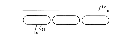
図2に示すように、マトリクス部40には、隔壁42に囲まれて区画された複数の画素領域41が設けれている。したがって、ノズル20の下にパネル1が搬送され、ノズルがNm方向に反復移動することにより、相対的にノズル20は軌道Ipを描くように、パネル上を移動することになる。ノズル20の軌道Ipは、画素領域41の長手方向に一列移動した後、次の列へと移動し、新たに画素領域41の長手方向に相対的に移動する。パネル1が、ノズル20の下方を通過する際にノズル20からインクが吐出され、図2に示すような軌跡を描きつつ、次々に画素領域41にインクが塗布されていく。
As shown in FIG. 2, the
インクは、インクジェット法の吐出のようにノズルから断続的に液滴が吐出されるのではなく、ノズル20から非断続的に連続して吐出されていくため、軌道Ipが示すように、インクは画素領域41および画素領域41の長手方向にある隔壁上にも非断続的に連続して塗布される。したがって、インクは、画素領域41の長手方向に並ぶ複数の複数の画素領域41および隔壁42の上に非断続的な線状に塗布されていく。画素領域41は周囲を囲う隔壁42によって、底の浅いウエル状になっており、画素領域内に塗布されたインクは、領域内に広がる。
The ink is not intermittently ejected from the nozzle as in the ink jet method, but is intermittently ejected intermittently from the
図3−1は、インクが塗布後から乾燥する過程における2つの画素領域とその周辺の様子を模式的に示した平面図であり、図3−2はその長手方向断面図である。インクはノズルから吐出された後から徐々に乾燥し始める。そして、インクの塗布が完了後、乾燥工程において所定の雰囲気下に置かれ、インクから溶媒が蒸発し硬化して層が形成される。 FIG. 3A is a plan view schematically showing two pixel regions and their surroundings in the process of drying ink after application, and FIG. 3B is a longitudinal sectional view thereof. The ink starts to dry gradually after being ejected from the nozzle. Then, after the ink application is completed, the ink is placed in a predetermined atmosphere in the drying process, and the solvent is evaporated from the ink and hardened to form a layer.
ノズルから塗布されるインクは液状であり、表面張力を有し、また、乾燥する過程において収縮する。また、選択的にインクを画素領域41内へと塗布するため、隔壁42は撥水処理が施されている。これらが主な要因となって、隔壁42上に塗布されたインク51は、乾燥する間に、画素領域41内方向Mへと引っ張られて、隔壁42上から画素領域41内へ流れ落ち、最終的には画素領域41内で層の一部を構成する。
The ink applied from the nozzle is liquid, has surface tension, and shrinks during the drying process. Further, in order to selectively apply ink into the
マトリクス部40のように、長辺を有する矩形上の形状の画素領域41が設けられている場合、インクジェット装置などを用いてインクが画素領域内に点状に塗布されると、被印刷体に着弾したインクは、ある程度画素領域内に広がるものの、インクの表面張力などの影響で、長手方向の端部まで十分に広がらない場合があり得る。十分に長手方向の端部まで広がらない場合、乾燥後にその部分に層が形成されない、あるいは層が設計された厚さに対して不十分になるおそれがある。
In the case where a
しかし、本発明の第1の実施形態では、インクを非断続的に連続して吐出し、画素領域41および画素領域41の長手方向にある隔壁42上に非断続的に連続してインクを塗布しながら、画素領域41の長手方向に並ぶ複数の画素領域41および隔壁42の上に線状にインクを塗布していく。インクは長手方向に非断続的な線状に塗布されているため、隔壁42上に塗布されたインク51は長手方向の左右いずれかの画素領域41内へは引き込まれやすい。そのため、画素領域41内に点状に塗布した場合に不足しがちな長手方向端部へとインクが隔壁上から補助的に供給され得ることになる。このようにして、長手方向端部での層形成不良を抑制することができる。
However, in the first embodiment of the present invention, the ink is ejected intermittently and continuously, and the ink is continuously and intermittently applied onto the
また、インクは長手方向に非断続的な線状に塗布されているため、画素領域41内へ繋がるインクに引っ張られ、短手方向の画素領域(図3では不図示)方向へは流れにくい。他方、隔壁頭部にインクを点状または非連続的状に塗布したのでは、所望の方向へとインクが流れ落ちる確率は下がるものと推測される。したがって、短手方向に並ぶ各列ごとに、画素領域に異なる成分を塗布する場合には、本発明の第1の実施形態のようにインクを塗布することにより、短手方向の画素領域間での汚染や混色などを防止し得る。
In addition, since the ink is applied in a non-intermittent linear shape in the longitudinal direction, the ink is pulled by the ink connected to the
単に吐出するインク量を増やし、例えば、画素が形成されるマトリクス全面にインクを塗布するのでは、画素領域41の短手方向へのインクの溢れが起き易く、混色等の原因となる。他方、本発明の第1の実施形態に示すように、インクを画素領域41の長手方向に非断続的な線状に塗布することにより、乾燥する過程で層厚が不足しがちな部分へ、インクを短手方向のインク溢れや混色なく、補足し得る。
For example, if the amount of ink to be ejected is simply increased, and ink is applied to the entire surface of the matrix on which the pixels are formed, ink overflows in the short direction of the
隔壁42の表面は、インクが残存しにくいように撥水性を有することが好ましい。隔壁を構成する成分に撥水性の成分を混合させておいても良いし、あるいは、隔壁表面に撥水性の被膜を設けてもよい。少なくとも画素領域41の長手方向に面する隔壁表面が撥水性を備えることが好ましく、より好ましくは、隔壁42の表面全体が撥水性を備える。少なくとも、画素領域41の長手方向に面する隔壁表面が撥水性を有することにより、長手方向端部へとインクがより流れ込みやすくし得る。
The surface of the
インクとしては、層を形成する成分(以下、本明細書中で「層形成成分」という場合がある)およびインク溶媒を含む溶液または懸濁液が用いられる。層形成成分として、好ましくは、導電性高分子材料、発光材料などが挙げられる。これらの成分は有機EL素子を構成する層の材料として使用する機会が多く、またインク溶媒に溶解または分散させて、インクとして塗布するのに好適である。 As the ink, a solution or suspension containing a component for forming a layer (hereinafter sometimes referred to as “layer-forming component” in the present specification) and an ink solvent is used. Preferred examples of the layer forming component include conductive polymer materials and light emitting materials. These components have many opportunities to be used as materials for layers constituting the organic EL device, and are suitable for being dissolved or dispersed in an ink solvent and applied as ink.
インク溶媒は、層形成成分等の条件によって適宜選択してよい。本明細書においては、インク溶媒の用語は、特に断らない限り、層形成成分を溶解させる液体および層形成成分を分散させる液体の双方を含む概念として用いる。インク溶媒として、好ましくは、揮発性、層形成成分の溶解性または分散性などに関し、インク溶媒としての好ましい諸要件を満たすことが好適である。インク溶媒として好ましくは、例えば、水、アルコール溶媒、グリコール溶媒、エーテル溶媒、エステル溶媒、含塩素溶媒および芳香族炭化水素溶媒からなる群より選ばれる1種またはこれらの2種以上の混合物が挙げられる。アルコール溶媒としては、例えば、メタノール、エタノール、プロパノール、イソプロパノール、ブタノールなどが挙げられる。グリコール溶媒としては、エチレングリコール、プロピレングリコール等が挙げられる。エーテル溶媒としては、例えば、テオトラヒドロンフラン、メトキシベンゼン等が挙げられる。エステル溶媒としては、例えば、酢酸エチル、酢酸ブチル等が挙げられる。含塩素溶媒としては、クロロホルム、クロロベンゼン、塩化メチレン等が挙げられる。芳香族炭化水素溶媒としては、例えば、トルエン、キシレン、トリメチルベンゼン、テトラメチルベンゼン等が挙げられる。 The ink solvent may be appropriately selected depending on conditions such as layer forming components. In this specification, the term “ink solvent” is used as a concept including both a liquid for dissolving a layer forming component and a liquid for dispersing a layer forming component, unless otherwise specified. As the ink solvent, it is preferable to satisfy various requirements as an ink solvent in terms of volatility, solubility or dispersibility of the layer forming component, and the like. The ink solvent is preferably, for example, one or a mixture of two or more selected from the group consisting of water, alcohol solvents, glycol solvents, ether solvents, ester solvents, chlorine-containing solvents and aromatic hydrocarbon solvents. . Examples of the alcohol solvent include methanol, ethanol, propanol, isopropanol, butanol and the like. Examples of the glycol solvent include ethylene glycol and propylene glycol. Examples of the ether solvent include theotrahydrofuran, methoxybenzene and the like. Examples of the ester solvent include ethyl acetate and butyl acetate. Examples of the chlorine-containing solvent include chloroform, chlorobenzene, and methylene chloride. Examples of the aromatic hydrocarbon solvent include toluene, xylene, trimethylbenzene, tetramethylbenzene and the like.
前記塗布工程において、吐出されるインクの粘度は、好ましくは、3cP以上、13cP以下、より好ましくは5cP以上、10cP以下である。このような粘度に調整することにより、インクを塗りむら少なく塗布し、良好な層を形成しやすい。 In the coating step, the viscosity of the ejected ink is preferably 3 cP or more and 13 cP or less, more preferably 5 cP or more and 10 cP or less. By adjusting to such a viscosity, it is easy to apply ink with less unevenness and form a good layer.
層形成成分を含むインクは、非断続的に連続して吐出される。インクを吐出する装置としては、例えば、ノズルプリンティング装置などが挙げられる。ノズルプリンティング装置は、微小なノズルからインクを連続的に吐出することができる装置である。ノズルプリンティング装置は、微細な線幅に安定して非断続的な連続線状に塗布するのに好適である。 The ink containing the layer forming component is discharged intermittently and continuously. Examples of the apparatus that ejects ink include a nozzle printing apparatus. The nozzle printing apparatus is an apparatus that can continuously eject ink from minute nozzles. The nozzle printing apparatus is suitable for coating in a non-intermittent continuous line stably with a fine line width.
塗布工程が完了した後、インクの乾燥が行われる。インクの乾燥工程では、インクから溶媒を留去させ、層形成成分を固定させる。作業速度効率の観点からは、インクの乾燥は短時間で完了できるほど好ましい一方、他方では、インクが画素領域内に全体に十分に広がり、均等な膜厚を形成するに至るように促すことが好ましい。インクの粘度、インク溶媒の種類などにもよるが、乾燥工程における好ましい一形態としては、20℃以上、90℃以下の温度条件下の空気中で、インクを乾燥させる形態が挙げられる。温度条件として、より好ましくは、20℃以上、40℃以下が挙げられる。このような条件下でインクを乾燥させることにより、画素領域内にインクが十分に展開し、画素領域内に均一な膜厚の層を形成を促進し、成膜不良などの弊害を抑制し得る。また、上記のような乾燥後、インクを焼成する工程を設けてもよい。 After the coating process is completed, the ink is dried. In the ink drying process, the solvent is distilled off from the ink to fix the layer forming components. From the viewpoint of working speed efficiency, it is preferable that ink drying be completed in a short time. On the other hand, the ink is sufficiently spread throughout the pixel area to encourage the formation of a uniform film thickness. preferable. Although it depends on the viscosity of the ink, the type of ink solvent, and the like, a preferred form in the drying step is a form in which the ink is dried in air under a temperature condition of 20 ° C. or higher and 90 ° C. or lower. As temperature conditions, More preferably, 20 degreeC or more and 40 degrees C or less are mentioned. By drying the ink under such conditions, the ink can be sufficiently developed in the pixel region, promoting the formation of a layer having a uniform film thickness in the pixel region, and adverse effects such as film formation defects can be suppressed. . Moreover, you may provide the process of baking an ink after the above drying.
(1−2)有機EL素子の構造
次に、本発明の製造方法により製造し得る有機EL装置に実装される有機EL素子の実施形態について、より具体的に説明する。有機エレクトロルミネッセンス素子は、少なくとも一対の電極と当該電極間に挟まれた、有機化合物を含む発光層を含む積層体で形成される。積層体を構成する層は、下記に説明するとおり、電極および発光層以外にも、様々な種類の層を設けてよい。また、層の積層順序等も様々な変形例をとり得る。
(1-2) Structure of Organic EL Element Next, the embodiment of the organic EL element mounted on the organic EL device that can be manufactured by the manufacturing method of the present invention will be described more specifically. The organic electroluminescence element is formed of a laminate including a light emitting layer containing an organic compound and sandwiched between at least a pair of electrodes and the electrodes. As described below, the layers constituting the laminate may be provided with various types of layers in addition to the electrodes and the light emitting layer. In addition, the layer stacking order and the like can be variously modified.
本発明の製造方法おいて製造される有機EL素子は、下記の有機EL素子に限定されるわけではない。また、本発明の製造方法においては、有機EL素子を構成する積層体のうちの少なくとも一層を形成する工程において、上記に説明した実施形態などに示されるような、所定の塗布工程と乾燥工程とを含む。したがって、他の層の形成においては、他の方法により層を形成させてもよい。下記においては、他の方法による層形成法も例示する。また、一般に、有機EL素子を構成する各層は極めて薄いものであり、その層形成には各種の成膜方法を採用し得る。そのため以下の説明においては、層形成のことを成膜という場合がある。 The organic EL device manufactured by the manufacturing method of the present invention is not limited to the following organic EL device. In the manufacturing method of the present invention, in the step of forming at least one layer of the laminate constituting the organic EL element, a predetermined coating step and a drying step as shown in the embodiment described above, including. Therefore, in forming other layers, the layers may be formed by other methods. In the following, other layer forming methods are also exemplified. In general, each layer constituting the organic EL element is extremely thin, and various film forming methods can be employed for forming the layer. Therefore, in the following description, the layer formation may be referred to as film formation.
有機EL素子は、陽極、発光層及び陰極を必須に有するのに加えて、前記陽極と前記発光層との間、及び/又は前記発光層と前記陰極との間にさらに他の層を有することができる。 In addition to having an anode, a light emitting layer and a cathode as essential, the organic EL device has another layer between the anode and the light emitting layer and / or between the light emitting layer and the cathode. Can do.
陰極と発光層の間に設け得る層としては、電子注入層、電子輸送層、正孔ブロック層等が挙げられる。電子注入層及び電子輸送層の両方が設けられる場合、陰極に近い層が電子注入層となり、発光層に近い層が電子輸送層となる。 Examples of the layer that can be provided between the cathode and the light emitting layer include an electron injection layer, an electron transport layer, and a hole blocking layer. When both the electron injection layer and the electron transport layer are provided, the layer close to the cathode is the electron injection layer, and the layer close to the light emitting layer is the electron transport layer.
電子注入層は、陰極からの電子注入効率を改善する機能を有する層であり、電子輸送層は、陰極、電子注入層又は陰極により近い電子輸送層からの電子注入を改善する機能を有する層である。また、電子注入層、若しくは電子輸送層が正孔の輸送を堰き止める機能を有する場合には、これらの層が正孔ブロック層を兼ねることがある。 The electron injection layer is a layer having a function of improving electron injection efficiency from the cathode, and the electron transport layer is a layer having a function of improving electron injection from the cathode, the electron injection layer or the electron transport layer closer to the cathode. is there. In addition, when the electron injection layer or the electron transport layer has a function of blocking hole transport, these layers may also serve as the hole blocking layer.
陽極と発光層の間に設けるものとしては、正孔注入層、正孔輸送層、電子ブロック層等があげられる。正孔注入層及び正孔輸送層の両方が設けられる場合、陽極に近い層が正孔注入層となり、発光層に近い層が正孔輸送層となる。 Examples of what is provided between the anode and the light emitting layer include a hole injection layer, a hole transport layer, and an electron block layer. When both the hole injection layer and the hole transport layer are provided, the layer close to the anode is the hole injection layer, and the layer close to the light emitting layer is the hole transport layer.
正孔注入層は、陽極からの正孔注入効率を改善する機能を有する層であり、正孔輸送層とは、陽極、正孔注入層又は陽極により近い正孔輸送層からの正孔注入を改善する機能を有する層である。また、正孔注入層、又は正孔輸送層が電子の輸送を堰き止める機能を有する場合には、これらの層が電子ブロック層を兼ねることがある。 The hole injection layer is a layer having a function of improving the hole injection efficiency from the anode, and the hole transport layer is a hole injection layer from the anode, the hole injection layer or the hole transport layer closer to the anode. It is a layer having a function of improving. In addition, when the hole injection layer or the hole transport layer has a function of blocking electron transport, these layers may also serve as an electron block layer.
有機EL素子において、発光層は通常1層設けられるが、これに限らず2層以上の発光層を設けることもできる。その場合、2層以上の発光層は、直接接して積層することもでき、かかる層の間に発光層以外の層を設けることができる。 In an organic EL element, one light emitting layer is usually provided, but not limited to this, two or more light emitting layers may be provided. In that case, two or more light-emitting layers can be stacked in direct contact with each other, and a layer other than the light-emitting layer can be provided between the layers.
さらに具体的には、有機EL素子は、下記の層構成のいずれかを有することができる:
a) 陽極/正孔注入層/正孔輸送層/発光層/電子輸送層/電子注入層/陰極
b) 陽極/正孔注入層/正孔輸送層/発光層/電子輸送層/陰極
c) 陽極/正孔注入層/正孔輸送層/発光層/電子注入層/陰極
d) 陽極/正孔注入層/正孔輸送層/発光層/陰極
e) 陽極/正孔注入層/発光層/電子輸送層/電子注入層/陰極
f) 陽極/正孔注入層/発光層/電子輸送層/陰極
g) 陽極/正孔注入層/発光層/電子注入層/陰極
h) 陽極/正孔注入層/発光層/陰極
i) 陽極/正孔輸送層/発光層/電子輸送層/電子注入層/陰極
j) 陽極/正孔輸送層/発光層/電子輸送層/陰極
k) 陽極/正孔輸送層/発光層/電子注入層/陰極
l) 陽極/正孔輸送層/発光層/陰極
m) 陽極/発光層/電子輸送層/電子注入層/陰極
n) 陽極/発光層/電子輸送層/陰極
o) 陽極/発光層/電子注入層/陰極
p) 陽極/発光層/陰極
(ここで、/は各層が隣接して積層されていることを示す。以下同じ。)
More specifically, the organic EL device can have any of the following layer configurations:
a) Anode / hole injection layer / hole transport layer / light emitting layer / electron transport layer / electron injection layer / cathode
b) Anode / hole injection layer / hole transport layer / light emitting layer / electron transport layer / cathode
c) Anode / hole injection layer / hole transport layer / light emitting layer / electron injection layer / cathode
d) Anode / hole injection layer / hole transport layer / light emitting layer / cathode
e) Anode / hole injection layer / light emitting layer / electron transport layer / electron injection layer / cathode
f) Anode / hole injection layer / light emitting layer / electron transport layer / cathode
g) Anode / hole injection layer / light emitting layer / electron injection layer / cathode
h) Anode / hole injection layer / light emitting layer / cathode
i) Anode / hole transport layer / light emitting layer / electron transport layer / electron injection layer / cathode
j) Anode / hole transport layer / light emitting layer / electron transport layer / cathode
k) Anode / hole transport layer / light emitting layer / electron injection layer / cathode
l) Anode / hole transport layer / light emitting layer / cathode
m) Anode / light-emitting layer / electron transport layer / electron injection layer / cathode
n) Anode / light emitting layer / electron transport layer / cathode
o) Anode / light emitting layer / electron injection layer / cathode
p) Anode / light emitting layer / cathode (where “/” indicates that each layer is laminated adjacently; the same shall apply hereinafter).
(1−3)有機EL素子を構成する各層の材料および層形成方法
次に、有機EL素子を構成する各層の材料及び形成方法について、より具体的に説明する。なお、上記の塗布工程および乾燥工程を採用して形成する少なくとも一層以外については、下記に例示される他の成膜方法を採用しても良い。
(1-3) Material and Layer Forming Method of Each Layer Constructing Organic EL Element Next, the material and forming method of each layer constituting the organic EL element will be described more specifically. In addition, you may employ | adopt the other film-forming method illustrated below except at least one layer formed by employ | adopting said application | coating process and a drying process.
<基板>
本発明の有機EL素子を構成する基板は、電極を形成し、有機物の層を形成する際に変化しないものであればよく、例えばガラス、プラスチック、高分子フィルム、シリコン基板、金属板、これらを積層したものなどが用いられる。
<Board>
The substrate constituting the organic EL device of the present invention may be any substrate as long as it does not change when an electrode is formed and an organic layer is formed, such as glass, plastic, polymer film, silicon substrate, metal plate, and the like. A laminated material is used.
<陽極>
有機EL素子の陽極としては、光を透過可能な透明電極を用いることが、陽極を通して発光する素子を構成しうるため好ましい。かかる透明電極としては、電気伝導度の高い金属酸化物、金属硫化物や金属の薄膜を用いることができ、透過率の高いものが好適に利用でき、用いる有機層により適宜、選択して用いる。具体的には、酸化インジウム、酸化亜鉛、酸化スズ、ITO、インジウム亜鉛酸化物(Indium Zinc Oxide:略称IZO)から成る薄膜や、金、白金、銀、銅、アルミニウム、またはこれらの金属を少なくとも1種類以上含む合金等が用いられる。
<Anode>
As the anode of the organic EL element, it is preferable to use a transparent electrode that can transmit light because an element that emits light through the anode can be configured. As such a transparent electrode, a metal oxide, metal sulfide or metal thin film having high electrical conductivity can be used, and a material having a high transmittance can be suitably used, which is appropriately selected depending on the organic layer to be used. Specifically, at least one of a thin film made of indium oxide, zinc oxide, tin oxide, ITO, indium zinc oxide (abbreviated as IZO), gold, platinum, silver, copper, aluminum, or a metal thereof is used. An alloy containing more than one type is used.
<正孔注入層>
正孔注入層は、陽極と正孔輸送層との間、または陽極と発光層との間に設けることができる。正孔注入層を構成する正孔注入層材料としては、特に制限はないが、公知の材料を適宜用いることができ、例えばフェニルアミン系、スターバースト型アミン系、フタロシアニン系、ヒドラゾン誘導体、カルバゾール誘導体、トリアゾール誘導体、イミダゾール誘導体、アミノ基を有するオキサジアゾール誘導体、酸化バナジウム、酸化タンタル、酸化タングステン、酸化モリブデン、酸化ルテニウム、酸化アルミニウム等の酸化物、アモルファスカーボン、ポリアニリン、ポリチオフェン誘導体等が挙げられる。
<Hole injection layer>
The hole injection layer can be provided between the anode and the hole transport layer or between the anode and the light emitting layer. The hole injection layer material constituting the hole injection layer is not particularly limited, but known materials can be used as appropriate, for example, phenylamine-based, starburst-type amine-based, phthalocyanine-based, hydrazone derivatives, carbazole derivatives. , Triazole derivatives, imidazole derivatives, oxadiazole derivatives having an amino group, oxides such as vanadium oxide, tantalum oxide, tungsten oxide, molybdenum oxide, ruthenium oxide, and aluminum oxide, amorphous carbon, polyaniline, and polythiophene derivatives.
<正孔輸送層>
正孔輸送層を構成する正孔輸送層材料としては特に制限はないが、例えばN,N’−ジフェニル−N,N’−ジ(3−メチルフェニル)4,4’−ジアミノビフェニル(TPD)、NPB(4,4’−bis[N−(1−naphthyl)−N−phenylamino]biphenyl)等の芳香族アミン誘導体、ポリビニルカルバゾール若しくはその誘導体、ポリシラン若しくはその誘導体、側鎖若しくは主鎖に芳香族アミンを有するポリシロキサン誘導体、ピラゾリン誘導体、アリールアミン誘導体、スチルベン誘導体、トリフェニルジアミン誘導体、ポリアニリン若しくはその誘導体、ポリチオフェン若しくはその誘導体、ポリアリールアミン若しくはその誘導体、ポリピロール若しくはその誘導体、ポリ(p−フェニレンビニレン)若しくはその誘導体、又はポリ(2,5−チエニレンビニレン)若しくはその誘導体などが例示される。
<Hole transport layer>
The hole transport layer material constituting the hole transport layer is not particularly limited. For example, N, N′-diphenyl-N, N′-di (3-methylphenyl) 4,4′-diaminobiphenyl (TPD) , NPB (4,4′-bis [N- (1-naphthyl) -N-phenylamino] biphenyl), etc., polyvinylcarbazole or derivatives thereof, polysilane or derivatives thereof, aromatic in side chain or main chain Polysiloxane derivative having amine, pyrazoline derivative, arylamine derivative, stilbene derivative, triphenyldiamine derivative, polyaniline or derivative thereof, polythiophene or derivative thereof, polyarylamine or derivative thereof, polypyrrole or derivative thereof, poly (p-phenylene vinylene) ) Or a derivative thereof, or poly (2,5-thienylene vinylene) or a derivative thereof is exemplified.
<発光層>
発光層は、有機化合物を含む。通常、主として蛍光またはりん光を発光する有機物(低分子化合物および高分子化合物)が含まれる。なお、さらにドーパント材料を含んでいてもよい。本発明において用いることができる発光層を形成する材料としては、例えば、以下の色素系材料、金属錯体系材料、高分子系材料、およびドーパント材料などが挙げられる。
<Light emitting layer>
The light emitting layer contains an organic compound. Usually, organic substances (low molecular compounds and high molecular compounds) that mainly emit fluorescence or phosphorescence are included. Further, a dopant material may be further included. Examples of the material for forming the light emitting layer that can be used in the present invention include the following dye-based materials, metal complex-based materials, polymer-based materials, and dopant materials.
[色素系材料]
色素系材料としては、例えば、シクロペンダミン誘導体、テトラフェニルブタジエン誘導体化合物、トリフェニルアミン誘導体、オキサジアゾール誘導体、ピラゾロキノリン誘導体、ジスチリルベンゼン誘導体、ジスチリルアリーレン誘導体、ピロール誘導体、チオフェン環化合物、ピリジン環化合物、ペリノン誘導体、ペリレン誘導体、オリゴチオフェン誘導体、トリフマニルアミン誘導体、オキサジアゾールダイマー、ピラゾリンダイマーなどが挙げられる。
[Dye-based materials]
Examples of dye-based materials include cyclopentamine derivatives, tetraphenylbutadiene derivative compounds, triphenylamine derivatives, oxadiazole derivatives, pyrazoloquinoline derivatives, distyrylbenzene derivatives, distyrylarylene derivatives, pyrrole derivatives, thiophene ring compounds. Pyridine ring compounds, perinone derivatives, perylene derivatives, oligothiophene derivatives, trifumanylamine derivatives, oxadiazole dimers, pyrazoline dimers, and the like.
[金属錯体系材料]
金属錯体系材料としては、例えば、イリジウム錯体、白金錯体等の三重項励起状態からの発光を有する金属錯体、アルミキノリノール錯体、ベンゾキノリノールベリリウム錯体、ベンゾオキサゾリル亜鉛錯体、ベンゾチアゾール亜鉛錯体、アゾメチル亜鉛錯体、ポルフィリン亜鉛錯体、ユーロピウム錯体など、中心金属に、Al、Zn、BeなどまたはTb、Eu、Dyなどの希土類金属を有し、配位子にオキサジアゾール、チアジアゾール、フェニルピリジン、フェニルベンゾイミダゾール、キノリン構造などを有する金属錯体などを挙げることができる。
[Metal complex materials]
Examples of the metal complex material include metal complexes that emit light from triplet excited states such as iridium complexes and platinum complexes, aluminum quinolinol complexes, benzoquinolinol beryllium complexes, benzoxazolyl zinc complexes, benzothiazole zinc complexes, azomethyls. Zinc complex, porphyrin zinc complex, europium complex, etc., which has Al, Zn, Be or the like as the central metal or rare earth metal such as Tb, Eu, or Dy, and the ligand is oxadiazole, thiadiazole, phenylpyridine, phenylbenzo Examples thereof include metal complexes having an imidazole or quinoline structure.
[高分子系材料]
高分子系材料としては、ポリパラフェニレンビニレン誘導体、ポリチオフェン誘導体、ポリパラフェニレン誘導体、ポリシラン誘導体、ポリアセチレン誘導体、ポリフルオレン誘導体、ポリビニルカルバゾール誘導体、上記色素体や金属錯体系発光材料を高分子化したものなどが挙げられる。
[Polymer material]
Polymeric materials include polyparaphenylene vinylene derivatives, polythiophene derivatives, polyparaphenylene derivatives, polysilane derivatives, polyacetylene derivatives, polyfluorene derivatives, polyvinylcarbazole derivatives, and polymerized chromophores and metal complex light emitting materials. Etc.
[ドーパント材料]
発光層中に発光効率の向上や発光波長を変化させるなどの目的で、ドーパントを添加することができる。このようなドーパントとしては、例えば、ペリレン誘導体、クマリン誘導体、ルブレン誘導体、キナクリドン誘導体、スクアリウム誘導体、ポルフィリン誘導体、スチリル系色素、テトラセン誘導体、ピラゾロン誘導体、デカシクレン、フェノキサゾンなどを挙げることができる。なお、このような発光層の厚さは、通常約2nm〜2000nmである。
[Dopant material]
A dopant can be added to the light emitting layer for the purpose of improving the light emission efficiency and changing the light emission wavelength. Examples of such dopants include perylene derivatives, coumarin derivatives, rubrene derivatives, quinacridone derivatives, squalium derivatives, porphyrin derivatives, styryl dyes, tetracene derivatives, pyrazolone derivatives, decacyclene, phenoxazone, and the like. In addition, the thickness of such a light emitting layer is usually about 2 nm-2000 nm.
<電子輸送層>
電子輸送層を構成する電子輸送材料としては、公知のものが使用でき、オキサジアゾール誘導体、アントラキノジメタン若しくはその誘導体、ベンゾキノン若しくはその誘導体、ナフトキノン若しくはその誘導体、アントラキノン若しくはその誘導体、テトラシアノアンスラキノジメタン若しくはその誘導体、フルオレノン誘導体、ジフェニルジシアノエチレン若しくはその誘導体、ジフェノキノン誘導体、又は8−ヒドロキシキノリン若しくはその誘導体の金属錯体、ポリキノリン若しくはその誘導体、ポリキノキサリン若しくはその誘導体、ポリフルオレン若しくはその誘導体等が例示される。
<Electron transport layer>
As the electron transport material constituting the electron transport layer, known materials can be used, such as oxadiazole derivatives, anthraquinodimethane or derivatives thereof, benzoquinone or derivatives thereof, naphthoquinone or derivatives thereof, anthraquinones or derivatives thereof, tetracyanoanthra Quinodimethane or derivatives thereof, fluorenone derivatives, diphenyldicyanoethylene or derivatives thereof, diphenoquinone derivatives, or metal complexes of 8-hydroxyquinoline or derivatives thereof, polyquinoline or derivatives thereof, polyquinoxaline or derivatives thereof, polyfluorene or derivatives thereof, etc. Illustrated.
<電子注入層>
電子注入層は、電子輸送層と陰極との間、または発光層と陰極との間に設けられる。電子注入層としては、発光層の種類に応じて、アルカリ金属やアルカリ土類金属、或いは前記金属を1種類以上含む合金、或いは前記金属の酸化物、ハロゲン化物及び炭酸化物、或いは前記物質の混合物などが挙げられる。
<Electron injection layer>
The electron injection layer is provided between the electron transport layer and the cathode or between the light emitting layer and the cathode. Depending on the type of the light emitting layer, the electron injection layer may be an alkali metal or alkaline earth metal, an alloy containing one or more of the above metals, or an oxide, halide and carbonate of the metal, or a mixture of the above substances. Etc.
<陰極材料>
陰極の材料としては、仕事関数の小さく発光層への電子注入が容易な材料及び/又は電気伝導度が高い材料及び/又は可視光反射率の高い材料が好ましい。金属では、アルカリ金属やアルカリ土類金属、遷移金属やIII−B族金属を用いることができる。
<Cathode material>
As a material for the cathode, a material having a small work function and easily injecting electrons into the light emitting layer and / or a material having a high electric conductivity and / or a material having a high visible light reflectance are preferable. As the metal, an alkali metal, an alkaline earth metal, a transition metal, or a group III-B metal can be used.
(1−4)有機EL装置の製造
本発明の製造方法により製造し得る有機EL装置は、上記のようにして有機EL素子で構成された画素が複数実装された装置である。電気的配線、駆動手段等の設置については、通常の有機EL装置の製造における様々な態様を採用し得る。
(1-4) Manufacture of Organic EL Device An organic EL device that can be manufactured by the manufacturing method of the present invention is a device in which a plurality of pixels configured with organic EL elements as described above are mounted. Regarding the installation of electrical wiring, driving means, etc., various modes in the manufacture of a normal organic EL device can be adopted.
本発明の製造方法により製造し得る有機EL装置は、面状光源、セグメント表示装置、ドットマトリックス表示装置、液晶表示装置のバックライトとして用いることができる。 The organic EL device that can be manufactured by the manufacturing method of the present invention can be used as a backlight of a planar light source, a segment display device, a dot matrix display device, and a liquid crystal display device.
本発明の有機EL装置を用いて面状の発光を得るためには、面状の陽極と陰極が重なり合うように配置すればよい。また、パターン状の発光を得るためには、前記面状の発光素子の表面にパターン状の窓を設けたマスクを設置する方法、非発光部の有機物層を極端に厚く形成し実質的に非発光とする方法、陽極または陰極のいずれか一方、または両方の電極をパターン状に形成する方法がある。これらのいずれかの方法でパターンを形成し、いくつかの電極を独立にON/OFFできるように配置することにより、数字や文字、簡単な記号などを表示できるセグメントタイプの表示装置が得られる。更に、ドットマトリックス素子とするためには、陽極と陰極をともにストライプ状に形成して直交するように配置するパッシブマトリックス用基板、あるいは薄膜トランジスタを配置した画素単位で制御を行うアクティブマトリックス用基板を用いればよい。さらに、発光色の異なる発光材料を塗り分ける方法や、カラーフィルターまたは蛍光変換フィルターを用いる方法により、部分カラー表示、マルチカラー表示が可能となる。これらの表示素子は、コンピュータ、テレビ、携帯端末、携帯電話、カーナビゲーション、ビデオカメラのビューファインダーなどの表示装置として用いることができる。 In order to obtain planar light emission using the organic EL device of the present invention, the planar anode and cathode may be arranged so as to overlap each other. In addition, in order to obtain pattern-like light emission, a method of installing a mask provided with a pattern-like window on the surface of the planar light-emitting element, an organic material layer of a non-light-emitting portion is formed extremely thick and substantially non- There are a method of emitting light and a method of forming either one of the anode or the cathode or both electrodes in a pattern. By forming a pattern by any of these methods and arranging several electrodes so that they can be turned on and off independently, a segment type display device capable of displaying numbers, letters, simple symbols, and the like can be obtained. Furthermore, in order to obtain a dot matrix element, a passive matrix substrate in which anodes and cathodes are both formed in stripes and arranged so as to be orthogonal to each other, or an active matrix substrate in which thin film transistors are arranged and controlled in units of pixels is used. That's fine. Furthermore, partial color display and multi-color display can be performed by separately applying light emitting materials having different emission colors or using a color filter or a fluorescence conversion filter. These display elements can be used as display devices for computers, televisions, mobile terminals, mobile phones, car navigation systems, video camera viewfinders, and the like.
さらに、前記面状の発光装置は、自発光薄型であり、液晶表示装置のバックライト用の面状光源、あるいは面状の照明用光源として好適に用いることができる。また、フレキシブルな基板を用いれば、曲面状の光源や表示装置としても使用できる。 Furthermore, the planar light-emitting device is self-luminous and thin, and can be suitably used as a planar light source for a backlight of a liquid crystal display device or a planar illumination light source. If a flexible substrate is used, it can be used as a curved light source or display device.
2.本発明の第1の実施形態の変形例1
第1の実施形態の変形例1について、図4を参照しつつ説明する。変形例1は、上記第1の実施形態と異なる点のみ説明し、他の点にいては第1の実施形態と同様の構成が採用される。図4に示すように、変形例1においては、画素領域41が千鳥模様状に配置されている。図4に示す変形例1では、画素領域41の長手方向Laに連なる一列L1および列L1と平行に並ぶ列L2〜L6の各列において、各画素領域41が一列に直線上に並んでいる。他方、列L1〜L6の各列の横手方向に並ぶ画素領域41同士は、直線上に一列並ぶようには配置されておらず、相互に位置がずれていてもよい。このようなマトリクス基板でも本発明の製造方法は適用可能である。
2.
3.本発明の第1の実施形態の変形例2乃至5
第1の実施形態の変形例2〜5について、図5−1から図5−5を参照しつつ説明する。変形例2〜5は、上記第1の実施形態と異なる点のみ説明し、他の点については第1の実施形態と同様の構成が採用される。
3. Modifications 2 to 5 of the first embodiment of the present invention
Modifications 2 to 5 of the first embodiment will be described with reference to FIGS. In Modifications 2 to 5, only points different from the first embodiment will be described, and the same configuration as that of the first embodiment is adopted for other points.
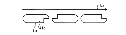
ここで説明する変形例2〜5は、画素領域の平面形状に係る変形例である。有機EL装置に実装される有機EL素子は、開口率を高める目的などにより様々な形状的な工夫が凝らされる場合がある。本発明では、画素領域の平面形状は、長辺または長軸を有する平面形状を有していればよい。長辺を有する平面形状としては、長辺を有する四角形およびこの部分的変形形状が含まれる。長辺を有する四角形としては、長方形、平行四辺形、および台形が挙げられる。長軸を有する平面形状には、例えば、楕円形、長対角線を有する菱形、2以上の円形または楕円形が融合した形状、およびこれらの部分的変形形状などが挙げられる。長辺または長軸を有する平面形状には、円そのもの、および正方形そのものは含まれない。 Modified examples 2 to 5 described here are modified examples related to the planar shape of the pixel region. The organic EL element mounted on the organic EL device may be devised in various shapes depending on the purpose of increasing the aperture ratio. In the present invention, the planar shape of the pixel region only needs to have a planar shape having a long side or a long axis. The planar shape having a long side includes a quadrangle having a long side and this partially deformed shape. Examples of the rectangle having a long side include a rectangle, a parallelogram, and a trapezoid. Examples of the planar shape having the long axis include an ellipse, a rhombus having a long diagonal line, a shape in which two or more circles or ellipses are fused, and a partially deformed shape thereof. A planar shape having a long side or a long axis does not include a circle itself or a square itself.
上記のように第1の実施形態では、画素領域41の平面形状は略長方形であり、長辺Lsを有し、また、その角部が丸められている(図5−1)。
図5−2に示す変形例2では、画素領域41aの平面形状が、長辺Lsを有する長方形である。上記第1の実施形態の場合と異なり、角部は丸められていない。長方形状の画素領域41aの長手方向はLaにて示される通りである。
図5−3に示す変形例3では、画素領域41bの平面形状が、長軸Lxを有する楕円形である。楕円形状の画素領域41bの長手方向はLaにて示される通りである。
図5−4に示す変形例4では、画素領域41aの平面形状は、第1の実施形態に示す切り欠き部のある形状である。変形例4のように、長手方向を定めることができる長辺Lsを特定し得る形状であれば、切り欠き部等により異形の長方形であってもよい。不図示であるが、楕円形に切り欠き部が設けられていてもよい。
変形例5として、図5−5に示すように、中央部にくびれがある形状であってもよい。変形例5の形状における画素領域41の長軸はLxで示され、その長手方向はLaにて示される通りである。
As described above, in the first embodiment, the planar shape of the
In Modification 2 shown in FIG. 5B, the planar shape of the
In the third modification illustrated in FIG. 5C, the planar shape of the
In
As a modified example 5, as shown in FIG. 5-5, a shape with a constriction at the center may be used. The major axis of the
4.本発明の第2の実施形態
上記第1の実施形態においても説明したとおり、本発明の製造方法では、画素領域の短手方向間でのインクの汚染、混色を簡便に防止し得る。そのため本発明の製造方法は、複数の画素が設けられる表示エリア部上において、一列に1種の画素を設け、隣接する他の列に他種の画素を設ける場合などに好適に採用し得るものである。
4). Second Embodiment of the Present Invention As described in the first embodiment, the manufacturing method of the present invention can easily prevent ink contamination and color mixing between the short sides of the pixel region. For this reason, the manufacturing method of the present invention can be suitably employed when, for example, one type of pixel is provided in one column and another type of pixel is provided in another adjacent column on a display area portion in which a plurality of pixels are provided. It is.
本発明の第2の実施形態では、複数の画素が画素領域の長手方向に一列に配置され、当該列が画素領域の短手方向に複数連接されてなる表示エリア部を備える有機エレクトロルミネッセンス装置を製造する場合に、塗布工程において、画素領域の長手方向の一列に第1の層成分および第1のインク溶媒を含む第1のインクを塗布し、隣接する列の画素領域には第1の層成分と異なる第2の層成分および第1のインク溶媒を含む第2のインクを塗布する。第1の層成分と第2の層成分とは異なる成分であるが、第1のインク溶媒と第2のインク溶媒とは、同じであっても、異なっていてもよい。 In the second embodiment of the present invention, there is provided an organic electroluminescence device including a display area unit in which a plurality of pixels are arranged in a row in a longitudinal direction of a pixel region, and a plurality of the columns are connected in a short direction of the pixel region. When manufacturing, in the coating process, the first ink containing the first layer component and the first ink solvent is applied to one column in the longitudinal direction of the pixel region, and the first layer is applied to the pixel region in the adjacent column. A second ink containing a second layer component different from the component and the first ink solvent is applied. Although the first layer component and the second layer component are different components, the first ink solvent and the second ink solvent may be the same or different.
好ましい一形態として、第1および第2の層成分が、それぞれ色の異なる発光材料である形態が挙げられる。本発明の第2の実施形態のより具体的な適用例として、画素領域の長手方向の第1の列に、赤色、緑色および青色からなる群より選ばれる1色を発光する第1の有機エレクトロルミネッセンス素子を形成し、第1の列に隣接する一方の列に、第1の有機エレクトロルミネッセンス素子の発光色とは異なる1色を発光する第2の有機エレクトロルミネッセンス素子が形成し、第1の列と隣接する他方の列に、第1および第2の有機エレクトロルミネッセンス素子の発光色とは異なる1色を発光する有機エレクトロルミネッセンス素子が形成する形態が提供される。 As one preferable mode, a mode in which the first and second layer components are light-emitting materials having different colors can be mentioned. As a more specific application example of the second embodiment of the present invention, the first organic electroluminescence that emits one color selected from the group consisting of red, green, and blue in the first column in the longitudinal direction of the pixel region. A luminescence element is formed, and a second organic electroluminescence element that emits one color different from the emission color of the first organic electroluminescence element is formed in one column adjacent to the first column. An embodiment is provided in which an organic electroluminescence element that emits one color different from the emission color of the first and second organic electroluminescence elements is formed in the other row adjacent to the row.
第2の実施形態の変形例を図6を参照しつつ説明する。図6中、第1の実施形態にて既に説明した事項については、同じ符号を付け、その説明を省略する。
図6に示すように、インクの供給には、3つのノズル(3連ノズル)21が備えられた装置が用いられる。3連ノズルの各ノズルはそれぞれ、赤色発光材料を含むインクを吐出するノズルNR、緑色発光材料を含むインクを吐出するノズルNG、青色発光材料を含むインクを吐出するノズルNBである。3連ノズル21は、当初位置(P1)に待機する。所定の位置あわせ完了後、3つのノズルからそれぞれのインクを非断続的に連続して吐出しながら、移動方向Nm1に移動する。3連ノズル21が位置(P2)に到達すると、パネル1を搬送方向Ddに移動し、3連ノズル21が位置(P3)に達した時点でパネルの移動を停止する。3連ノズル21は、移動方向Nm3に移動し、位置(P4)に達した時点で停止する。以下、このような稼働を繰り返し、順次パネル上の画素領域にインクを塗布していく。
A modification of the second embodiment will be described with reference to FIG. In FIG. 6, the items already described in the first embodiment are denoted by the same reference numerals, and the description thereof is omitted.
As shown in FIG. 6, an apparatus provided with three nozzles (triple nozzles) 21 is used for supplying ink. Each nozzle of the triple nozzle is a nozzle N B to the discharge nozzle N R for ejecting ink containing a red light-emitting material, a nozzle N G for ejecting ink containing a green light-emitting material, an ink containing a blue luminescent material. The
第1の実施形態と同様、インクは、画素領域41の長手方向(すなわち、ノズルの移動方向Nm1またはNm3)に非断続的な線状に塗布されているため、長手方向の左右いずれかの画素領域41内へは引き込まれやすい。そのため、インクが不足しがちな長手方向端部へとインクが隔壁42上から補助的に供給され得ることになる。また、画素領域41内へ繋がるインクに引っ張られ、短手方向の画素領域41方向へは流れにくい。したがって、短手方向の画素領域41間での汚染や混色などを防止し得る。
As in the first embodiment, since the ink is applied in an intermittent line shape in the longitudinal direction of the pixel region 41 (that is, the nozzle movement direction Nm 1 or Nm 3 ), it is left or right in the longitudinal direction. Are easily drawn into the
以下、本発明の実施例を示し、本発明についてより具体的に説明するが、本発明が下記実施例に限定されるものではない。
<実施例1>
(1)素子の製造
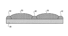
図7に示すように、隔壁(バンク)42が形成され、多数の画素領域41が形成されているアクティブマトリクス基板を用意した。図7は、画素領域41が形成されたアクティブマトリクスの一部を示す図である。画素領域41には、ITO電極により、陽極が形成されている。本アクティブマトリクス基板を、RIE装置(SAMCO社製、RIE−200L)を用いて酸素プラズマ処理(3aPa、30W、30SCCM、3分)およびCF4プラズマ処理(20aPa、20W、20SCCM、2分)を行ったところ、隔壁42上に選択的に撥水処理が施された。画素領域41の陽極上に、ノズルプリンティング装置(大日本スクリーン社製、NP−300G)を用い、PEDOTインクを塗布した。ノズルプリンティング装置のノズルから、途絶えることなく連続してインクを吐出させつつ、相対的にノズルが画素領域41の長手方向に移動するようにアクティブマトリクス基板を移動させ、、アクティブマトリクス基板上の一列をなす複数の画素領域41にインクを塗布した。図8に、図7のI−I’線におけるインク塗布後の断面図(上面からの推定図)を示す。上記のようにして、図8に示すようにインク53が画素領域41内および隔壁42上に非断続的に連続して塗布されるようにした。なお、ノズルプリンティング装置に充填されたインクとして、PEDOT/PSS水溶液(H.C.Starck製、CH8000)を充填した。
(PEDOT:ポリエチレンジオキシチオフェン、PSS:ポリスチレンスルホン酸)
Hereinafter, examples of the present invention will be shown and the present invention will be described more specifically. However, the present invention is not limited to the following examples.
<Example 1>
(1) Manufacture of Elements As shown in FIG. 7, an active matrix substrate in which partition walls (banks) 42 are formed and a large number of
(PEDOT: polyethylene dioxythiophene, PSS: polystyrene sulfonic acid)
室温にてインクを20分自然乾燥した後、200℃に過熱したホットプレート(アズワン株式会社製、CHP−400D)上でインクを20分乾燥した。上面からアクティブマトリクスを拡大視認したところ、各画素領域において塗り残し部位は見られなかった。また、触針式段差計(KLA−Tencor Corporation社製P−16+)にて、形成された層の膜形状を測定したところ、良好な平坦性をもつPEDOT膜が形成されていることが確認できた。視認および触診式段差計の測定結果に基づく、乾燥後の断面形状を図9に示す。図9に示すように乾燥後のインク54(形成された層)は画素領域41内に十分広がっており、平坦性も良好であった。
After the ink was naturally dried at room temperature for 20 minutes, the ink was dried on a hot plate heated to 200 ° C. (manufactured by As One Co., Ltd., CHP-400D) for 20 minutes. When the active matrix was enlarged and visually confirmed from the upper surface, no unpainted portion was seen in each pixel region. Moreover, when the film shape of the formed layer was measured with a stylus type step gauge (P-16 + manufactured by KLA-Tencor Corporation), it was confirmed that a PEDOT film having good flatness was formed. It was. FIG. 9 shows a cross-sectional shape after drying based on the measurement results of the visual and palpation type step meters. As shown in FIG. 9, the dried ink 54 (formed layer) was sufficiently spread in the
このように、ノズルプリンティング装置にてPEDOTインクを塗布し、乾燥、焼成することにより、塗り残しがなく、良好な平坦性をもつ正孔注入層を形成することができた。この正孔注入層上に、同様にして発光層を形成し、発光層上に、真空蒸着法などを用いて陰極を形成することで、有機EL装置を製造できる。 Thus, by applying PEDOT ink with a nozzle printing apparatus, drying and baking, it was possible to form a hole injection layer having no flatness and good flatness. An organic EL device can be manufactured by forming a light emitting layer on the hole injection layer in the same manner, and forming a cathode on the light emitting layer using a vacuum deposition method or the like.
<比較例1>
ノズルプリンティング装置の代わりに、インクジェット装置(Litrex社製120L)を用い、隔壁42条にインクが乗らない様に、陽極の形成された画素領域41上に選択的にPEDOTインクを塗布した。その他の条件は、上記実施例1と同様とした。インクジェット装置を用い、各画素領域41の陽極上に選択的にインク53を滴下させたため、インク塗布後のアクティブマトリクス断面は、上面からの視認により、図10のようになっているものと推定された。
<Comparative Example 1>
Instead of the nozzle printing apparatus, an ink jet apparatus (120L manufactured by Litrex) was used, and PEDOT ink was selectively applied on the
さらに、実施例1と同様に塗布後のインク53を乾燥させた。乾燥後の断面図を、図11に示す。上面からアクティブマトリクスを拡大視認したところ、各画素領域において塗り残し部位が見られた。また、また、触針式段差計(KLA−Tencor Corporation社製P−16+)にて、形成された層を測定した結果からも、画素領域内に膜形成不良があることが確認できた。視認および触診式段差計の測定結果に基づく、乾燥後の断面形状を図11に示す。図11に示すように、乾燥後のインク54(形成された層)は画素領域41内において膜厚にむらがあり、一部には基板30の表面がむき出しになっている部位もあった。
Further, in the same manner as in Example 1, the
以上のように、本発明は有機EL装置に関連する産業分野において有用である。 As described above, the present invention is useful in the industrial field related to the organic EL device.
1 パネル
20 ノズル
21 3連ノズル
30 支持基板
40 マトリクス部
41、41a〜41d 画素領域
42 隔壁
51 インク(隔壁上)
52 インク(画素領域内)
53 インク(乾燥前)
54 インク(乾燥後)
Dd パネルの搬送方向
Ip ノズルの軌道
L1〜L6 画素領域の長手方向の各一列
La 長手方向(ノズルの進行方向)
Ls 長辺
Lx 長軸
M インクの移動
NR ノズル(赤色インク吐出用)
NG ノズル(緑色インク吐出用)
NB ノズル(青色インク吐出用)
Nm ノズルの移動方向
Nm1〜Nm3 ノズルの移動方向
P1〜P4 位置
DESCRIPTION OF
52 ink (in pixel area)
53 ink (before drying)
54 Ink (after drying)
Dd Panel transport direction Ip Nozzle trajectory L 1 to L 6 One row in the longitudinal direction of the pixel region La Longitudinal direction (advancing direction of the nozzle)
Ls Long side Lx Long axis M Ink movement N R nozzle (for red ink ejection)
NG nozzle (for discharging green ink)
N B nozzle (for blue ink ejection)
Nm Nozzle movement direction Nm 1 to Nm 3 Nozzle movement direction P 1 to P 4 positions
Claims (12)
前記画素が形成される画素領域は、当該領域を囲む隔壁により区画され、長辺または長軸を有する平面形状を有し、
前記有機エレクトロルミネッセンス素子は、前記積層体を構成する層を前記画素領域内に順次積層して形成され、前記積層体を構成する層のうちの少なくとも一層を形成する工程は、塗布工程と乾燥工程とを含み、
前記塗布工程において、前記層を形成する成分とインク溶媒とを含むインクを非断続的に連続して吐出し、前記画素領域および当該画素領域の長手方向にある隔壁上に非断続的に連続して前記インクを塗布しながら、前記画素領域の長手方向に並ぶ複数の画素領域上に線状に前記インクを塗布し、
前記乾燥工程において、塗布された前記インクを乾燥する、
有機エレクトロルミネッセンス装置の製造方法。 Manufacture of an organic electroluminescence device comprising a plurality of pixels, and the pixel comprising at least a pair of electrodes and a laminate including a light emitting layer containing an organic compound sandwiched between the electrodes A method,
The pixel region in which the pixel is formed is partitioned by a partition wall surrounding the region, and has a planar shape having a long side or a long axis,
The organic electroluminescence element is formed by sequentially laminating the layers constituting the laminated body in the pixel region, and the steps of forming at least one of the layers constituting the laminated body are a coating process and a drying process. Including
In the coating step, the ink including the component forming the layer and the ink solvent is intermittently ejected continuously and intermittently continuously on the pixel region and the partition in the longitudinal direction of the pixel region. While applying the ink, apply the ink linearly on a plurality of pixel regions arranged in the longitudinal direction of the pixel region,
In the drying step, the applied ink is dried.
A method for manufacturing an organic electroluminescence device.
前記塗布工程においては、前記画素領域の長手方向の一列に第1の層成分と第1のインク溶媒とを含む第1のインクが塗布され、隣接する列の画素領域には第1の層成分と異なる第2の層成分と第2のインク溶媒とを含む第2のインクが塗布される、請求項1から9のいずれか一項に記載の有機エレクトロルミネッセンス装置の製造方法。 The organic electroluminescence device includes a display area unit in which a plurality of pixels are arranged in a row in the longitudinal direction of the pixel region, and the columns are connected in a short direction in the pixel region,
In the coating step, the first ink containing the first layer component and the first ink solvent is applied to one column in the longitudinal direction of the pixel region, and the first layer component is applied to the pixel region in the adjacent column. 10. The method of manufacturing an organic electroluminescence device according to claim 1, wherein a second ink containing a second layer component different from the above and a second ink solvent is applied.
Priority Applications (1)
| Application Number | Priority Date | Filing Date | Title |
|---|---|---|---|
| JP2008086877A JP2009238708A (en) | 2008-03-28 | 2008-03-28 | Manufacturing method for organic electroluminescent apparatus |
Applications Claiming Priority (1)
| Application Number | Priority Date | Filing Date | Title |
|---|---|---|---|
| JP2008086877A JP2009238708A (en) | 2008-03-28 | 2008-03-28 | Manufacturing method for organic electroluminescent apparatus |
Publications (1)
| Publication Number | Publication Date |
|---|---|
| JP2009238708A true JP2009238708A (en) | 2009-10-15 |
Family
ID=41252381
Family Applications (1)
| Application Number | Title | Priority Date | Filing Date |
|---|---|---|---|
| JP2008086877A Pending JP2009238708A (en) | 2008-03-28 | 2008-03-28 | Manufacturing method for organic electroluminescent apparatus |
Country Status (1)
| Country | Link |
|---|---|
| JP (1) | JP2009238708A (en) |
Cited By (4)
| Publication number | Priority date | Publication date | Assignee | Title |
|---|---|---|---|---|
| WO2011065288A1 (en) * | 2009-11-24 | 2011-06-03 | 住友化学株式会社 | Manufacturing method of light emitting device |
| WO2011105330A1 (en) * | 2010-02-25 | 2011-09-01 | 住友化学株式会社 | Light emitting device and a method for producing same |
| CN102754529A (en) * | 2010-02-09 | 2012-10-24 | 住友化学株式会社 | Method for producing light-emitting device |
| CN112086499A (en) * | 2014-09-03 | 2020-12-15 | 精工爱普生株式会社 | Organic electroluminescent device and electronic apparatus |
Citations (2)
| Publication number | Priority date | Publication date | Assignee | Title |
|---|---|---|---|---|
| JP2007188862A (en) * | 2005-12-13 | 2007-07-26 | Canon Inc | Organic el light-emitting device and its manufacturing method |
| WO2008032720A1 (en) * | 2006-09-13 | 2008-03-20 | Sumitomo Chemical Company, Limited | Polymer compound and polymer light-emitting device |
-
2008
- 2008-03-28 JP JP2008086877A patent/JP2009238708A/en active Pending
Patent Citations (2)
| Publication number | Priority date | Publication date | Assignee | Title |
|---|---|---|---|---|
| JP2007188862A (en) * | 2005-12-13 | 2007-07-26 | Canon Inc | Organic el light-emitting device and its manufacturing method |
| WO2008032720A1 (en) * | 2006-09-13 | 2008-03-20 | Sumitomo Chemical Company, Limited | Polymer compound and polymer light-emitting device |
Cited By (7)
| Publication number | Priority date | Publication date | Assignee | Title |
|---|---|---|---|---|
| WO2011065288A1 (en) * | 2009-11-24 | 2011-06-03 | 住友化学株式会社 | Manufacturing method of light emitting device |
| JP2011113646A (en) * | 2009-11-24 | 2011-06-09 | Sumitomo Chemical Co Ltd | Method of manufacturing light emitting device |
| CN102754529A (en) * | 2010-02-09 | 2012-10-24 | 住友化学株式会社 | Method for producing light-emitting device |
| WO2011105330A1 (en) * | 2010-02-25 | 2011-09-01 | 住友化学株式会社 | Light emitting device and a method for producing same |
| US9356251B2 (en) | 2010-02-25 | 2016-05-31 | Sumitomo Chemical Company, Limited | Light-emitting device including a first resistance layer with a creeping-up portion |
| CN112086499A (en) * | 2014-09-03 | 2020-12-15 | 精工爱普生株式会社 | Organic electroluminescent device and electronic apparatus |
| CN112086499B (en) * | 2014-09-03 | 2023-06-30 | 精工爱普生株式会社 | Organic electroluminescent device and electronic apparatus |
Similar Documents
| Publication | Publication Date | Title |
|---|---|---|
| TWI355862B (en) | Methods for producing full-color organic electrolu | |
| US8507897B2 (en) | Organic EL element having a partition with a step, method for manufacturing organic EL element, organic EL device, and electronic apparatus | |
| KR100645485B1 (en) | Display device, method of manufacturing the same, and electronic apparatus | |
| WO2011049224A1 (en) | Substrate for organic electroluminescence device and method of manufacturing organic electroluminescence device employing same | |
| WO2010061966A1 (en) | Light emission device and method for manufacturing same | |
| WO2010084897A1 (en) | Ink-jet printing ink for organic electroluminescent element, and process for production of organic electroluminescent element | |
| JP2010067543A (en) | Ink for printing | |
| JP2004355913A (en) | Process for manufacturing organic electroluminescence device | |
| US20110121282A1 (en) | Manufacturing method of organic electroluminescence element, light-emitting device, and display device | |
| WO2010035643A1 (en) | Substrate for pattern coating and organic el element | |
| JP2010033971A (en) | Organic electroluminescent element and its manufacturing method | |
| WO2011049225A1 (en) | Substrate for organic electroluminescence device and method of manufacturing organic electroluminescence device employing same | |
| JP2009064642A (en) | Manufacturing method of organic electroluminescent display device, and manufacturing apparatus | |
| WO2011007849A1 (en) | Liquid column coating ink, organic el element production method, and organic el device provided with said organic el element | |
| JP2009238709A (en) | Method and apparatus for manufacturing organic electroluminescent element | |
| JP2009238708A (en) | Manufacturing method for organic electroluminescent apparatus | |
| JP2010073579A (en) | Method of manufacturing organic el element, and coater | |
| WO2011118654A1 (en) | Method for manufacturing light-emitting device | |
| JP5317873B2 (en) | SUBSTRATE FOR ORGANIC EL ELEMENT, PROCESS FOR PRODUCING ORGANIC EL LAYER, AND APPARATUS PROVIDED WITH ORGANIC EL ELEMENT MOUNTED ON SUBSTRATE FOR ORGANIC EL ELEMENT | |
| WO2017082173A1 (en) | Method for manufacturing organic el device, and organic el device | |
| JP4957318B2 (en) | Manufacturing method of organic EL device | |
| JP2010160946A (en) | Method for manufacturing organic electroluminescence device | |
| JP2010160945A (en) | Method for manufacturing organic electroluminescence device | |
| JP2009245599A (en) | Light-emitting device, and method of manufacturing light-emitting device | |
| JP2010205528A (en) | Manufacturing method of organic electroluminescent device |
Legal Events
| Date | Code | Title | Description |
|---|---|---|---|
| A621 | Written request for application examination |
Free format text: JAPANESE INTERMEDIATE CODE: A621 Effective date: 20110203 |
|
| A977 | Report on retrieval |
Free format text: JAPANESE INTERMEDIATE CODE: A971007 Effective date: 20120316 |
|
| A131 | Notification of reasons for refusal |
Free format text: JAPANESE INTERMEDIATE CODE: A131 Effective date: 20120403 |
|
| A02 | Decision of refusal |
Free format text: JAPANESE INTERMEDIATE CODE: A02 Effective date: 20121002 |