JP2009227701A - Phosphor and method for producing it - Google Patents
Phosphor and method for producing it Download PDFInfo
- Publication number
- JP2009227701A JP2009227701A JP2008071109A JP2008071109A JP2009227701A JP 2009227701 A JP2009227701 A JP 2009227701A JP 2008071109 A JP2008071109 A JP 2008071109A JP 2008071109 A JP2008071109 A JP 2008071109A JP 2009227701 A JP2009227701 A JP 2009227701A
- Authority
- JP
- Japan
- Prior art keywords
- light
- phosphor
- range
- light emitting
- phosphor according
- Prior art date
- Legal status (The legal status is an assumption and is not a legal conclusion. Google has not performed a legal analysis and makes no representation as to the accuracy of the status listed.)
- Pending
Links
Images
Classifications
-
- C—CHEMISTRY; METALLURGY
- C09—DYES; PAINTS; POLISHES; NATURAL RESINS; ADHESIVES; COMPOSITIONS NOT OTHERWISE PROVIDED FOR; APPLICATIONS OF MATERIALS NOT OTHERWISE PROVIDED FOR
- C09K—MATERIALS FOR MISCELLANEOUS APPLICATIONS, NOT PROVIDED FOR ELSEWHERE
- C09K11/00—Luminescent, e.g. electroluminescent, chemiluminescent materials
- C09K11/08—Luminescent, e.g. electroluminescent, chemiluminescent materials containing inorganic luminescent materials
- C09K11/0883—Arsenides; Nitrides; Phosphides
-
- C—CHEMISTRY; METALLURGY
- C09—DYES; PAINTS; POLISHES; NATURAL RESINS; ADHESIVES; COMPOSITIONS NOT OTHERWISE PROVIDED FOR; APPLICATIONS OF MATERIALS NOT OTHERWISE PROVIDED FOR
- C09K—MATERIALS FOR MISCELLANEOUS APPLICATIONS, NOT PROVIDED FOR ELSEWHERE
- C09K11/00—Luminescent, e.g. electroluminescent, chemiluminescent materials
- C09K11/08—Luminescent, e.g. electroluminescent, chemiluminescent materials containing inorganic luminescent materials
- C09K11/77—Luminescent, e.g. electroluminescent, chemiluminescent materials containing inorganic luminescent materials containing rare earth metals
- C09K11/7783—Luminescent, e.g. electroluminescent, chemiluminescent materials containing inorganic luminescent materials containing rare earth metals containing two or more rare earth metals one of which being europium
- C09K11/77927—Silicon Nitrides or Silicon Oxynitrides
-
- H—ELECTRICITY
- H01—ELECTRIC ELEMENTS
- H01J—ELECTRIC DISCHARGE TUBES OR DISCHARGE LAMPS
- H01J61/00—Gas-discharge or vapour-discharge lamps
- H01J61/02—Details
- H01J61/38—Devices for influencing the colour or wavelength of the light
- H01J61/42—Devices for influencing the colour or wavelength of the light by transforming the wavelength of the light by luminescence
- H01J61/44—Devices characterised by the luminescent material
-
- H—ELECTRICITY
- H01—ELECTRIC ELEMENTS
- H01L—SEMICONDUCTOR DEVICES NOT COVERED BY CLASS H10
- H01L33/00—Semiconductor devices with at least one potential-jump barrier or surface barrier specially adapted for light emission; Processes or apparatus specially adapted for the manufacture or treatment thereof or of parts thereof; Details thereof
- H01L33/48—Semiconductor devices with at least one potential-jump barrier or surface barrier specially adapted for light emission; Processes or apparatus specially adapted for the manufacture or treatment thereof or of parts thereof; Details thereof characterised by the semiconductor body packages
- H01L33/50—Wavelength conversion elements
- H01L33/501—Wavelength conversion elements characterised by the materials, e.g. binder
- H01L33/502—Wavelength conversion materials
Landscapes
- Chemical & Material Sciences (AREA)
- Inorganic Chemistry (AREA)
- Engineering & Computer Science (AREA)
- Materials Engineering (AREA)
- Organic Chemistry (AREA)
- Luminescent Compositions (AREA)
- Led Device Packages (AREA)
Abstract
Description
本発明は、蛍光体およびその製造方法に関する。 The present invention relates to a phosphor and a manufacturing method thereof.
蛍光体は白色LED等の発光装置に用いられている。白色LEDは、発光素子と該発光素子が発する光の少なくとも一部により励起され発光する蛍光体とを有し、白色光を発する発光装置であり、それに用いる発光素子としては、青色光を発する発光素子(以下、青色LEDと記載することがある。)、近紫外光〜青紫色光を発する発光素子(以下、近紫外LEDと記載することがある。)が挙げられる。また、これらの発光素子が発する光により励起され発光する蛍光体として、特許文献1には、式(Ba,Eu)9Sc2Si6O24で表される蛍光体が記載されている。 The phosphor is used in a light emitting device such as a white LED. The white LED is a light emitting device that has a light emitting element and a phosphor that emits light by being excited by at least a part of light emitted from the light emitting element, and emits white light. Examples include an element (hereinafter sometimes referred to as a blue LED) and a light emitting element that emits near-ultraviolet light to blue-violet light (hereinafter sometimes referred to as a near-ultraviolet LED). In addition, as a phosphor that is excited by light emitted from these light emitting elements and emits light, Patent Document 1 describes a phosphor represented by the formula (Ba, Eu) 9 Sc 2 Si 6 O 24 .
上記式で表される蛍光体は特に緑色に発光することから、例えば、黄色に発光することのできるY3Al5O12:Ce蛍光体と組み合わせるなどして、演色性に優れる発光装置を得ることができる意味で有用なものの、未だ改良の余地はある。本発明の目的は、演色性を主とする発光特性をさらに改善することのできる発光装置を与え得る蛍光体を提供することにある。 Since the phosphor represented by the above formula emits green light in particular, for example, by combining with a Y 3 Al 5 O 12 : Ce phosphor capable of emitting yellow light, a light emitting device having excellent color rendering properties is obtained. Although useful in the sense that it can, there is still room for improvement. An object of the present invention is to provide a phosphor that can provide a light-emitting device that can further improve the light-emitting characteristics mainly of color rendering.
本発明者らは、鋭意研究を重ねた結果、本発明に至った。
すなわち本発明は、下記の発明を提供する。
<1>以下の式(1)で表される化合物におけるM2の少なくとも一部がM4(M4は三価カチオン元素を表す。)で置換され、該化合物におけるOの一部がM5(M5は三価アニオン元素を表す。)で置換され、該化合物におけるM1および/またはM2の一部が賦活元素で置換されてなる蛍光体。
aM1O・3M2O・6M3O2 (1)
(ここで、M1はBa、SrおよびCaからなる群より選ばれる1種以上のアルカリ土類金属元素を表し、M2はMgおよびZnからなる群より選ばれる1種以上の二価金属元素を表し、M3は四価金属元素を表し、aは3以上9以下の範囲の値である。)
<2>aの値が9である前記<1>記載の蛍光体。
<3>以下の式(2)で表される化合物におけるM1および/またはM2の一部が賦活元素で置換されてなる蛍光体。
M1 9(M2 3-1.5xM4 x)M3 6O24-1.5yM5 y (2)
(ここで、M1、M2、M3、M4およびM5は、それぞれ前記と同じ意味を有し、xは0を超え2以下の範囲の値であり、yは0を超え2以下の範囲の値である。)
<4>メルウィナイト(Merwinite)と同型の結晶構造を有する前記<2>または<3>に記載の蛍光体。
<5>M3がSiである前記<1>〜<4>のいずれかに記載の蛍光体。
<6>M4がScである前記<1>〜<5>のいずれかに記載の蛍光体。
<7>M5がNである前記<1>〜<6>のいずれかに記載の蛍光体。
<8>前記化合物におけるM1の一部が賦活元素で置換されてなる前記<1>〜<7>のいずれかに記載の蛍光体。
<9>賦活元素がEuである前記<1>〜<8>のいずれかに記載の蛍光体。
<10>M1、M3、M4、賦活元素、および必要に応じてM2を所定量含有する混合原料(ここで、M1、M2、M3およびM4は、それぞれ前記と同じ意味を有する。)を、酸素含有雰囲気中で焼成し、さらにM5含有雰囲気中(ここで、M5は前記と同じ意味を有する。)で焼成することを特徴とする蛍光体の製造方法。
<11>M5含有雰囲気が、アンモニア含有雰囲気である前記<10>記載の製造方法。
<12>前記<1>〜<9>のいずれかに記載の蛍光体を有する発光装置。
<13>発光素子と該発光素子が発する光の少なくとも一部により励起され発光する蛍光物質とを有する発光装置であって、該蛍光物質が前記<1>〜<9>のいずれかに記載の蛍光体を含有する発光装置。
<14>発光素子が発する光が、波長範囲を300nm以上780nm以下とする波長−発光強度曲線において最大発光強度となるところの波長(λMax)が350nm以上480nm以下の範囲にある光である前記<13>記載の発光装置。
As a result of intensive studies, the present inventors have reached the present invention.
That is, the present invention provides the following inventions.
<1> At least a part of M 2 in the compound represented by the following formula (1) is substituted with M 4 (M 4 represents a trivalent cation element), and a part of O in the compound is M 5. (M 5 represents a trivalent anion element), and a phosphor obtained by substituting a part of M 1 and / or M 2 in the compound with an activating element.
aM 1 O · 3M 2 O · 6M 3 O 2 (1)
(Here, M 1 represents one or more alkaline earth metal elements selected from the group consisting of Ba, Sr and Ca, and M 2 represents one or more divalent metal elements selected from the group consisting of Mg and Zn. M 3 represents a tetravalent metal element, and a is a value in the range of 3 to 9.
<2> The phosphor according to <1>, wherein the value of a is 9.
<3> A phosphor obtained by substituting a part of M 1 and / or M 2 in the compound represented by the following formula (2) with an activating element.
M 1 9 (M 2 3-1.5x M 4 x ) M 3 6 O 24-1.5y M 5 y (2)
(Here, M 1 , M 2 , M 3 , M 4 and M 5 each have the same meaning as described above, x is a value in the range of more than 0 and 2 or less, and y is more than 0 and 2 or less. Value in the range.)
<4> The phosphor according to <2> or <3>, which has the same crystal structure as that of merwinite.
<5> The phosphor according to any one of <1> to <4>, wherein M 3 is Si.
<6> The phosphor according to any one of <1> to <5>, wherein M 4 is Sc.
<7> The phosphor according to any one of <1> to <6>, wherein M 5 is N.
<8> The phosphor according to any one of <1> to <7>, wherein a part of M 1 in the compound is substituted with an activating element.
<9> The phosphor according to any one of <1> to <8>, wherein the activation element is Eu.
<10> M 1 , M 3 , M 4 , an activation element, and a mixed raw material containing a predetermined amount of M 2 as required (where M 1 , M 2 , M 3 and M 4 are the same as described above, respectively) Is fired in an oxygen-containing atmosphere, and further fired in an M 5 -containing atmosphere (where M 5 has the same meaning as described above).
<11> The method according to <10>, wherein the atmosphere containing M 5 is an ammonia-containing atmosphere.
<12> A light emitting device comprising the phosphor according to any one of <1> to <9>.
<13> A light-emitting device having a light-emitting element and a fluorescent material that emits light by being excited by at least a part of light emitted from the light-emitting element, wherein the fluorescent material is any one of <1> to <9>. A light-emitting device containing a phosphor.
<14> The light emitted from the light emitting element is light having a wavelength (λMax) in a range of 350 nm or more and 480 nm or less where the maximum emission intensity is obtained in a wavelength-luminescence intensity curve having a wavelength range of 300 nm or more and 780 nm or less. 13> The light-emitting device of description.
本発明によれば、演色性を主とする発光特性をさらに改善することのできる発光装置を与え得る蛍光体を提供することができる。本発明は、白色LEDなどの発光装置、すなわち蛍光体の励起源が青色LEDまたは紫外LEDの発する光である発光装置に好適であるばかりか、蛍光体の励起源が電子線である電子線励起発光装置(例えば、ブラウン管、フィールドエミッションディスプレイ、表面電界ディスプレイ等)、蛍光体の励起源が紫外線である紫外線励起発光装置(例えば、液晶ディスプレイ用バックライト、3波長型蛍光ランプ、高負荷蛍光ランプ等)、蛍光体の励起源が真空紫外線である真空紫外線励起発光装置(例えば、プラズマディスプレイパネル、希ガスランプ等)、蛍光体の励起源がX線である発光装置(X線撮像装置等)等にも適用可能であり、本発明は、工業的に極めて有用である。 ADVANTAGE OF THE INVENTION According to this invention, the fluorescent substance which can provide the light-emitting device which can further improve the light emission characteristic mainly having color rendering properties can be provided. The present invention is suitable not only for a light emitting device such as a white LED, that is, a light emitting device in which a phosphor excitation source is light emitted from a blue LED or an ultraviolet LED, but also in an electron beam excitation in which the phosphor excitation source is an electron beam. Light-emitting devices (for example, cathode ray tubes, field emission displays, surface electric field displays, etc.), UV-excited light-emitting devices (for example, backlights for liquid crystal displays, three-wavelength fluorescent lamps, high-load fluorescent lamps, etc.) ), A vacuum ultraviolet excitation light-emitting device (for example, a plasma display panel, a rare gas lamp, etc.) in which the phosphor excitation source is vacuum ultraviolet light, a light-emitting device (X-ray imaging device, etc.) in which the phosphor excitation source is X-ray, etc. The present invention is extremely useful industrially.
以下、本発明について詳しく説明する。
本発明の蛍光体は、以下の式(1)で表される化合物におけるM2の少なくとも一部がM4(M4は三価カチオン元素を表す。)で置換され、該化合物におけるOの一部がM5(M5は三価アニオン元素を表す。)で置換され、該化合物におけるM1および/またはM2の一部が賦活元素で置換されてなることを特徴とする。
aM1O・3M2O・6M3O2 (1)
(ここで、M1はBa、SrおよびCaからなる群より選ばれる1種以上のアルカリ土類金属元素を表し、M2はMgおよびZnからなる群より選ばれる1種以上の二価金属元素を表し、M3は四価金属元素を表し、aは3以上9以下の範囲の値である。)
The present invention will be described in detail below.
In the phosphor of the present invention, at least part of M 2 in the compound represented by the following formula (1) is substituted with M 4 (M 4 represents a trivalent cation element), and A part is substituted with M 5 (M 5 represents a trivalent anion element), and a part of M 1 and / or M 2 in the compound is substituted with an activating element.
aM 1 O · 3M 2 O · 6M 3 O 2 (1)
(Here, M 1 represents one or more alkaline earth metal elements selected from the group consisting of Ba, Sr and Ca, and M 2 represents one or more divalent metal elements selected from the group consisting of Mg and Zn. M 3 represents a tetravalent metal element, and a is a value in the range of 3 to 9.
上記において、aの値が3であるときの蛍光体の結晶構造としては、ディオプサイド(Diopside、透輝石)と同型の結晶構造を挙げることができ、aの値が6であるときの蛍光体の結晶構造としては、オケルマナイト(Akermanite、オケルマン石)と同型の結晶構造を挙げることができ、aの値が9であるときの蛍光体の結晶構造としては、メルウィナイト(Merwinite)と同型の結晶構造を挙げることができる。これらの中でも、本発明の効果をより高める観点では、aの値が9であることが好ましい。なお、これらの結晶構造は、粉末X線回折測定により、同定することができる。 In the above, the crystal structure of the phosphor when the value of a is 3 can be the same crystal structure as that of diopside, and the fluorescence when the value of a is 6 Examples of the crystal structure of the body include the same type of crystal structure as kermanite (Akermanite), and the crystal structure of the phosphor when the value of a is 9 includes the same type of crystal as merwinite (Merwinite). The structure can be mentioned. Among these, the value of a is preferably 9 from the viewpoint of further enhancing the effects of the present invention. These crystal structures can be identified by powder X-ray diffraction measurement.
aの値が9であるときの本発明の蛍光体としては、以下の式(2)で表される化合物におけるM1および/またはM2の一部が賦活元素で置換されてなる蛍光体を挙げることができ、好ましい実施形態である。さらにメルウィナイト(Merwinite)と同型の結晶構造を有することが好ましい。
M1 9(M2 3-1.5xM4 x)M3 6O24-1.5yM5 y (2)
(ここで、M1、M2、M3、M4およびM5は、それぞれ前記と同じ意味を有し、xは0を超え2以下の範囲の値であり、yは0を超え2以下の範囲の値である。)
As the phosphor of the present invention when the value of a is 9, a phosphor in which a part of M 1 and / or M 2 in the compound represented by the following formula (2) is substituted with an activating element is used. Which is a preferred embodiment. Further, it preferably has the same crystal structure as that of merwinite.
M 1 9 (M 2 3-1.5x M 4 x ) M 3 6 O 24-1.5y M 5 y (2)
(Here, M 1 , M 2 , M 3 , M 4 and M 5 each have the same meaning as described above, x is a value in the range of more than 0 and 2 or less, and y is more than 0 and 2 or less. Value in the range.)
本発明において、蛍光体の発光輝度、温度特性の観点から、M1は少なくともBaを含有することが好ましく、例えば、M1がBaであることを挙げることができる。 In the present invention, M 1 preferably contains at least Ba from the viewpoint of light emission luminance and temperature characteristics of the phosphor. For example, it can be mentioned that M 1 is Ba.
本発明において、蛍光体の結晶性を高める観点から、M2は少なくともMgを含有することが好ましく、例えば、M2がMgであることを挙げることができる。 In the present invention, from the viewpoint of enhancing the crystallinity of the phosphor, M 2 preferably contains at least Mg. For example, it can be mentioned that M 2 is Mg.
本発明において、M3の四価金属元素としては、Si、Ti、Ge、Zr、SnおよびHfからなる群より選ばれる1種以上の元素を挙げることができ、取り扱い容易性の観点から、M3は少なくともSiを含有することが好ましく、例えば、M3がSiであることを挙げることができる。 In the present invention, as the tetravalent metal element of M 3 , one or more elements selected from the group consisting of Si, Ti, Ge, Zr, Sn, and Hf can be exemplified. 3 preferably contains at least Si. For example, it can be mentioned that M 3 is Si.
本発明において、M4の三価カチオン元素としては、Al、Sc、Ga、Y、In、La、GdおよびLuからなる群より選ばれる1種以上の元素を挙げることができ、蛍光体の結晶性を高める観点から、M4は少なくともScを含有することが好ましく、例えば、M4がScであることを挙げることができる。 In the present invention, examples of the trivalent cation element of M 4 include one or more elements selected from the group consisting of Al, Sc, Ga, Y, In, La, Gd, and Lu. From the viewpoint of enhancing the properties, M 4 preferably contains at least Sc. For example, it can be mentioned that M 4 is Sc.
本発明において、M5の三価アニオン元素としては、Nを挙げることができる。 In the present invention, N may be mentioned as the trivalent anion element of M 5 .
本発明において、賦活元素としては、希土類元素およびMnの中から、適宜選択して用いることができる。発光輝度をより高める意味で、好ましい賦活元素はEuである。賦活元素がEuである場合には、Euの一部を共賦活元素で置換することにより、発光輝度がさらにより高くなる場合がある。共賦活元素としては、Al、Sc、Y、La、Gd、Ce、Pr、Nd、Pm、Sm、Tb、Dy、Ho、Er、Tm、Yb、Lu、Bi、Au、Ag、CuおよびMnからなる群より選ばれる1種以上の元素を挙げることができる。置換の割合としては、Euの50モル%以下が挙げられる。また、賦活元素は、上記式(1)または式(2)におけるM1の一部を置換することが好ましい。 In the present invention, the activation element can be appropriately selected from rare earth elements and Mn. In order to further increase the light emission luminance, a preferable activation element is Eu. When the activation element is Eu, the emission luminance may be further increased by substituting a part of Eu with the co-activation element. Co-activating elements include Al, Sc, Y, La, Gd, Ce, Pr, Nd, Pm, Sm, Tb, Dy, Ho, Er, Tm, Yb, Lu, Bi, Au, Ag, Cu, and Mn. One or more elements selected from the group consisting of: Examples of the substitution ratio include 50 mol% or less of Eu. Also, activating element, it is preferable to replace a portion of M 1 in the formula (1) or formula (2).
本発明において、xは0を超え2以下の範囲の値である。xをこの範囲で調整することで、任意の波長の発光を得ることができる。より具体的には、0を超え2以下の範囲において、xを大きくすればするほど、より長波長の発光を得ることができ、xを小さくすればするほど、より短波長の発光を得ることができる。また、yは0を超え2以下の範囲の値である。yをこの範囲で調整することで、任意の波長の発光を得ることができる。より具体的には、0を超え2以下の範囲において、yを大きくすればするほど、より長波長の発光を得ることができ、yを小さくすればするほど、より短波長の発光を得ることができる。また、安定な結晶構造を保つ意味では、x=yであることが好ましい。 In the present invention, x is a value in the range of more than 0 and 2 or less. Light having an arbitrary wavelength can be obtained by adjusting x in this range. More specifically, in the range of more than 0 and 2 or less, the longer x is, the longer wavelength light emission can be obtained, and the smaller x is, the shorter wavelength light emission is obtained. Can do. Moreover, y is a value in the range of more than 0 and 2 or less. Light having an arbitrary wavelength can be obtained by adjusting y within this range. More specifically, in the range of more than 0 and 2 or less, the longer the y, the longer the emission of light, and the smaller the y, the shorter the emission. Can do. In order to maintain a stable crystal structure, x = y is preferable.
次に、本発明の蛍光体を製造する方法について説明する。本発明の蛍光体は、焼成により本発明の蛍光体となり得る組成を含有する混合原料を焼成することにより製造することができる。例えば、M1、M3、M4、賦活元素、および必要に応じてM2を所定量含有する混合原料(ここで、M1、M2、M3およびM4は、それぞれ前記と同じ意味を有する。)を、酸素含有雰囲気中で焼成し、さらにM5含有雰囲気中(ここで、M5は前記と同じ意味を有する。)で焼成することにより製造することができる。 Next, a method for producing the phosphor of the present invention will be described. The phosphor of the present invention can be produced by firing a mixed raw material containing a composition that can be converted into the phosphor of the present invention by firing. For example, a mixed raw material containing a predetermined amount of M 1 , M 3 , M 4 , an activation element, and M 2 as required (where M 1 , M 2 , M 3 and M 4 have the same meaning as described above) Can be fired in an oxygen-containing atmosphere, and further in a M 5 -containing atmosphere (where M 5 has the same meaning as described above).
混合原料は、M1、M3、M4、賦活元素、および必要に応じてM2のそれぞれの金属元素を含有する化合物を所定の組成(本発明の蛍光体となり得る組成)となるように秤量し混合することにより得ることができる。該化合物としては、それぞれの金属元素の化合物で、例えば、酸化物を用いるか、または窒化物、水酸化物、炭酸塩、硝酸塩、ハロゲン化物、シュウ酸塩などを用いることができる。該化合物としてフッ化物、塩化物等のハロゲン化物を適量用いることにより、生成する蛍光体の結晶性、蛍光体を構成する粒子の平均粒径を制御することができる。この場合、ハロゲン化物は、反応促進剤(フラックス)としての役割を果たす場合もある。フラックスとしては、例えば、MgF2、CaF2、SrF2、BaF2、MgCl2、CaCl2、SrCl2、BaCl2、MgI2、CaI2、SrI2、BaI2などのハロゲン化物、NH4Cl、NH4Iなどのアンモニウム塩、B2O3、H3BO3などのホウ素化合物を挙げることができ、これらを混合原料として、あるいは、混合原料に適量添加して用いることができる。 The mixed raw material has a predetermined composition of M 1 , M 3 , M 4 , an activating element, and, if necessary, a compound containing each metal element of M 2 (a composition that can be a phosphor of the present invention). It can be obtained by weighing and mixing. As the compound, a compound of each metal element, for example, an oxide, or a nitride, hydroxide, carbonate, nitrate, halide, oxalate, or the like can be used. By using an appropriate amount of a halide such as fluoride or chloride as the compound, the crystallinity of the phosphor to be produced and the average particle diameter of the particles constituting the phosphor can be controlled. In this case, the halide may play a role as a reaction accelerator (flux). The flux, for example, MgF 2, CaF 2, SrF 2, BaF 2, MgCl 2, CaCl 2, SrCl 2, BaCl 2, MgI 2, CaI 2, SrI 2, halides such as BaI 2, NH 4 Cl, Examples thereof include ammonium salts such as NH 4 I and boron compounds such as B 2 O 3 and H 3 BO 3 , and these can be used as a mixed raw material or by adding an appropriate amount to the mixed raw material.
例えば、本発明において好ましい蛍光体の一つであるSr:Eu:Mg:Sc:Siのモル比が、2.97:0.03:0.5:0.5:2である蛍光体は、SrCO3、Eu2O3、MgO、Sc2O3およびSiO2の各原料をSr:Eu:Mg:Sc:Siのモル比が2.97:0.03:0.5:0.5:2となるように秤量、混合して得られる混合原料を酸素含有雰囲気中で焼成し、さらにM5含有雰囲気中(ここで、M5は前記と同じ意味を有する。)で焼成することにより製造することができる。 For example, a phosphor having a molar ratio of Sr: Eu: Mg: Sc: Si which is one of the preferred phosphors in the present invention is 2.97: 0.03: 0.5: 0.5: 2. Each raw material of SrCO 3 , Eu 2 O 3 , MgO, Sc 2 O 3, and SiO 2 has a molar ratio of Sr: Eu: Mg: Sc: Si of 2.97: 0.03: 0.5: 0.5: Produced by calcining a mixed raw material obtained by weighing and mixing so as to be 2 in an oxygen-containing atmosphere, and further firing in an M 5 -containing atmosphere (where M 5 has the same meaning as described above). can do.
前記の混合には、例えばボールミル、V型混合機、攪拌機等の通常工業的に用いられている装置を用いることができる。また、湿式混合、乾式混合のいずれによってもよい。また共沈などの晶析により、混合原料を得てもよい。 For the mixing, for example, a device that is usually used industrially, such as a ball mill, a V-type mixer, or a stirrer, can be used. Also, either wet mixing or dry mixing may be used. Further, a mixed raw material may be obtained by crystallization such as coprecipitation.
前記の混合原料の焼成は、組成にもよるが、例えば600℃以上1600℃以下の温度範囲にて、0.3時間以上100時間以下の時間範囲で保持して焼成することにより本発明の蛍光体を得ることができる。前記の焼成時の保持温度は、1100℃以上1400℃以下の温度であることが好ましい。 Although the firing of the mixed raw material depends on the composition, for example, the fluorescent material of the present invention can be fired by holding in a temperature range of 600 ° C. to 1600 ° C. for a time range of 0.3 hours to 100 hours. You can get a body. The holding temperature at the time of firing is preferably 1100 ° C. or higher and 1400 ° C. or lower.
焼成時の酸素含有雰囲気としては、酸素雰囲気、空気雰囲気などを挙げることができる。また、M5含有雰囲気として、M5がNである場合には、アンモニア含有雰囲気が好ましい。アンモニア含有雰囲気は、アンモニア雰囲気のほか、アンモニア−水素混合雰囲気、アンモニア−メタン混合雰囲気などのアンモニア混合雰囲気を挙げることができる。混合雰囲気におけるアンモニアの濃度を調整することで、蛍光体におけるNの量を調整することが可能である。また、蛍光体におけるNの量は、M4の量にも依存することがある。また例えば、N含有雰囲気として、0.1気圧以上の窒素雰囲気などの高圧窒素雰囲気も使用可能である。 Examples of the oxygen-containing atmosphere during firing include an oxygen atmosphere and an air atmosphere. Further, as the M 5 containing atmosphere, when M 5 is N, ammonia-containing atmosphere is preferred. Examples of the ammonia-containing atmosphere include an ammonia atmosphere such as an ammonia-hydrogen mixed atmosphere and an ammonia-methane mixed atmosphere in addition to the ammonia atmosphere. The amount of N in the phosphor can be adjusted by adjusting the concentration of ammonia in the mixed atmosphere. Also, the amount of N in the phosphor may depend on the amount of M 4 . For example, a high-pressure nitrogen atmosphere such as a nitrogen atmosphere of 0.1 atm or higher can be used as the N-containing atmosphere.
また、前記の焼成の前に、混合原料について、焼成時の保持温度未満の温度で保持して仮焼を行い、結晶水を除去したりした後に、前記の焼成を行うことも可能である。仮焼を行う雰囲気は、酸素含有雰囲気、不活性ガス雰囲気、還元性雰囲気のいずれでもよい。また仮焼後に粉砕することもできる。また、混合原料の一部または全部に、窒化物を用いた場合は、混合原料を、不活性ガス雰囲気、還元性雰囲気で焼成することによっても、本発明の蛍光体の製造が可能である。 In addition, before the firing, the mixed raw material may be calcined while being held at a temperature lower than the retention temperature at the time of firing, and the firing may be performed after removing crystal water. The atmosphere in which the calcination is performed may be any of an oxygen-containing atmosphere, an inert gas atmosphere, and a reducing atmosphere. Moreover, it can also grind | pulverize after calcination. In addition, when nitride is used for a part or all of the mixed raw material, the phosphor of the present invention can also be manufactured by firing the mixed raw material in an inert gas atmosphere or a reducing atmosphere.
また、本発明における蛍光体の組成の分析に関して、M1、M2、M3、M4の量は、例えば、高周波誘導結合プラズマを光源とした発光分析法(ICP分析法)により測定することができる。また、M5の量については、例えば、混合原料を酸素含有雰囲気中で焼成し、さらにM5含有雰囲気中で焼成する場合には、酸素含有雰囲気中で焼成した後の重量に対するM5含有雰囲気中で焼成した後の重量の増減から、測定することができる。この測定は、TG−DTA測定装置などの熱分析装置を用いて行ってもよい。 Regarding the analysis of the composition of the phosphor in the present invention, the amounts of M 1 , M 2 , M 3 , and M 4 are measured by, for example, an emission analysis method (ICP analysis method) using high frequency inductively coupled plasma as a light source. Can do. Regarding the amount of M 5 , for example, when the mixed raw material is baked in an oxygen-containing atmosphere and further baked in an M 5 -containing atmosphere, the M 5 -containing atmosphere relative to the weight after baking in the oxygen-containing atmosphere It can be measured from the increase / decrease in weight after firing in. This measurement may be performed using a thermal analysis device such as a TG-DTA measurement device.
さらに上記方法にて得られる蛍光体を、例えばボールミル、ジェットミル等を用いて粉砕することができる。また、洗浄、分級することができる。また、粉砕、焼成を2回以上行うこともできる。また、蛍光体の粒子表面を表面修飾材で被覆するなどの表面処理を施してもよい。表面修飾材としては、Si、Al、Ti、La、Y等を含有する無機物質を挙げることができる。 Furthermore, the phosphor obtained by the above method can be pulverized using, for example, a ball mill, a jet mill or the like. It can also be washed and classified. Further, pulverization and firing can be performed twice or more. Further, a surface treatment such as coating the surface of the phosphor particles with a surface modifier may be performed. Examples of the surface modifier include inorganic substances containing Si, Al, Ti, La, Y, and the like.
上記のようにして得られる本発明の蛍光体は、白色LED、液晶用バックライト、蛍光灯、プラズマディスプレイパネル、希ガスランプ、ブラウン管、FED、X線撮像装置、無機ELディスプレイ等の発光装置に用いることができる。 The phosphor of the present invention obtained as described above is used in light emitting devices such as white LEDs, liquid crystal backlights, fluorescent lamps, plasma display panels, rare gas lamps, cathode ray tubes, FEDs, X-ray imaging devices, inorganic EL displays, and the like. Can be used.
特に、本発明の蛍光体は、350nm以上480nm以下の範囲の波長の光、好ましくは380nm以上460nm以下の範囲の波長の光により励起され発光することができるので、発光素子として青色LEDまたは近紫外LEDを用い、該発光素子と該発光素子が発する波長範囲を300nm以上780nm以下とする波長−発光強度曲線において最大発光強度となるところの波長(λmax)が350nm以上480nm以下の範囲にある光、好ましくはλmaxが380nm以上460nm以下の範囲にある光の少なくとも一部により励起され発光する蛍光物質とを有する発光装置(白色LED)に用いることができる。この場合、該蛍光物質は、少なくとも本発明の蛍光体を含有していればよく、さらに後述のように他の蛍光体を含有するものであってもよい。 In particular, the phosphor of the present invention can be excited and emitted by light having a wavelength in the range of 350 nm to 480 nm, preferably light having a wavelength in the range of 380 nm to 460 nm. Light having a wavelength (λmax) in a range of 350 nm or more and 480 nm or less in a wavelength-luminescence intensity curve in which the light emitting element and the wavelength range emitted by the light emitting element are 300 nm or more and 780 nm or less using an LED, Preferably, it can be used for a light emitting device (white LED) having a fluorescent material that is excited by at least a part of light having a λmax in the range of 380 nm to 460 nm. In this case, the fluorescent material only needs to contain at least the phosphor of the present invention, and may further contain other phosphors as described later.
次に、発光装置に用いる発光素子について、青色LEDまたは近紫外LEDを例に挙げて、具体的に説明する。青色LEDまたは近紫外LEDは、例えば、特開平6−177423号公報、特開平11−191638号公報に開示されているような公知の技術により製造することができる。すなわち、基板上にn型の化合物半導体層(n型層)、化合物半導体からなる発光層(発光層)、p型の化合物半導体層(p型層)を積層した構造を有する。基板としては、サファイア、SiC、Siなどが挙げられる。化合物半導体層の積層方法としては、一般的に用いられているMOVPE(Metal Organic Vapor Phase Epitaxy)法、MBE(Molecular Beam Epitaxy)法などが挙げられる。発光層の化合物半導体の基本組成として、GaN、IniGa1-iN(0<i<1)、IniAljGa1-i-jN(0<i<1、0<j<1、i+j<1)等が用いられる。この組成を変化させることにより、発する光の波長すなわち近紫外光〜青紫色光または青色光の波長を変化させることができる。また、発光層に含まれる不純物の量を低く抑えておくことが好ましい。具体的には、不純物としてSi、Ge、2族元素の各元素を用いた場合、いずれもその濃度が1017cm-3以下であることが好ましい。発光層は単一量子井戸構造あるいは多重量子井戸構造としてもよい。また発光層の膜厚としては5Å以上300Å以下が好ましく、より好ましくは、10Å以上90Å以下である。膜厚が5Åより小さいかまたは300Åより大きいと発光素子の発光効率が十分でない場合がある。 Next, a light-emitting element used in the light-emitting device will be specifically described using a blue LED or a near-ultraviolet LED as an example. A blue LED or a near-ultraviolet LED can be manufactured by a known technique as disclosed in, for example, Japanese Patent Laid-Open Nos. 6-177423 and 11-191638. That is, it has a structure in which an n-type compound semiconductor layer (n-type layer), a light-emitting layer (light-emitting layer) made of a compound semiconductor, and a p-type compound semiconductor layer (p-type layer) are stacked on a substrate. Examples of the substrate include sapphire, SiC, Si and the like. As a method for laminating a compound semiconductor layer, a generally used MOVPE (Metal Organic Vapor Phase Epitaxy) method, MBE (Molecular Beam Epitaxy) method, and the like can be given. As the basic composition of the compound semiconductor of the light emitting layer, GaN, In i Ga 1-i N (0 <i <1), In i Al j Ga 1-ij N (0 <i <1, 0 <j <1, i + j <1) etc. are used. By changing this composition, the wavelength of the emitted light, that is, the wavelength of near-ultraviolet light to blue-violet light or blue light can be changed. In addition, it is preferable to keep the amount of impurities contained in the light emitting layer low. Specifically, when Si, Ge, or a group 2 element is used as an impurity, the concentration is preferably 10 17 cm −3 or less. The light emitting layer may have a single quantum well structure or a multiple quantum well structure. Further, the thickness of the light emitting layer is preferably 5 to 300 mm, more preferably 10 to 90 mm. If the film thickness is smaller than 5 mm or larger than 300 mm, the light emitting efficiency of the light emitting element may not be sufficient.
p型層およびn型層としては、発光層の化合物半導体のバンドギャップより大きなバンドギャップを有する化合物半導体を用いる。n型層とp型層との間に発光層を配置することで、発光素子を得ることができる。また、n型層と発光層との間、発光層とp型層との間には、必要に応じて組成、伝導性、ドーピング濃度の異なるいくつかの層を挿入してもよい。この挿入層の化合物半導体の基本組成としては、例えば、前記のIniAljGa1-i-jN(0<i<1、0<j<1、i+j<1)が挙げられ、この中で、発光層とは組成、伝導性、ドーピング濃度等を異なる組成を用いる。 As the p-type layer and the n-type layer, a compound semiconductor having a band gap larger than that of the compound semiconductor of the light emitting layer is used. A light emitting element can be obtained by disposing a light emitting layer between an n-type layer and a p-type layer. Moreover, you may insert several layers from which a composition, conductivity, and doping concentration differ between an n-type layer and a light emitting layer and between a light emitting layer and a p-type layer as needed. As the basic composition of the compound semiconductor of this insertion layer, for example, the above-mentioned In i Al j Ga 1-ij N (0 <i <1, 0 <j <1, i + j <1) can be mentioned, A composition having a different composition, conductivity, doping concentration, and the like from the light emitting layer is used.
発光層に隣接する二つの層を電荷注入層という。前記の挿入層がある場合には、その挿入層が電荷注入層となり、挿入層がない場合には、n型層、p型層が電荷注入層となる。発光層においては、この二つの電荷注入層により、正電荷および負電荷が注入され、この電荷同士が再結合することにより光を発する。この発光層に注入された電荷を効率的に再結合させ高強度の光を得るためには、n型層と発光層との間および発光層とp型層との間に、発光層のバンドギャップより大きなバンドギャップを有する挿入層を挿入して電荷注入層とした構造(いわゆるダブルヘテロ構造)を有する発光素子とすることが好ましい。電荷注入層と発光層とのバンドギャップの差は0.1eV以上であることが好ましい。電荷注入層と発光層とのバンドギャップの差が0.1eVより小さい場合、発光層へのキャリアの閉じ込めが十分でないことにより発光素子の発光効率が低下することがある。またこのバンドギャップの差は、より好ましくは0.3eV以上である。ただし、電荷注入層のバンドギャップが5eVを越えると電荷注入に必要な電圧が高くなるため、電荷注入層のバンドギャップは5eV以下が好ましい。また、電荷注入層の膜厚は、10Å以上、5000Å以下が好ましい。電荷注入層の膜厚が5Åより小さい場合あるいは5000Åより大きい場合は、発光素子の発光効率が低下する傾向にある。電荷注入層の膜厚は、より好ましくは10Å以上2000Å以下である。 Two layers adjacent to the light emitting layer are called charge injection layers. When the insertion layer is present, the insertion layer is a charge injection layer, and when there is no insertion layer, the n-type layer and the p-type layer are charge injection layers. In the light emitting layer, positive charges and negative charges are injected by the two charge injection layers, and light is emitted by recombination of these charges. In order to efficiently recombine the charges injected into the light emitting layer to obtain high intensity light, a band of the light emitting layer is provided between the n type layer and the light emitting layer and between the light emitting layer and the p type layer. A light-emitting element having a structure (so-called double heterostructure) in which an insertion layer having a band gap larger than the gap is inserted to form a charge injection layer is preferable. The difference in band gap between the charge injection layer and the light emitting layer is preferably 0.1 eV or more. When the difference in band gap between the charge injection layer and the light emitting layer is smaller than 0.1 eV, the light emission efficiency of the light emitting element may be lowered due to insufficient carrier confinement in the light emitting layer. The difference in band gap is more preferably 0.3 eV or more. However, if the band gap of the charge injection layer exceeds 5 eV, the voltage required for charge injection becomes high. Therefore, the band gap of the charge injection layer is preferably 5 eV or less. The thickness of the charge injection layer is preferably 10 to 5000 mm. When the thickness of the charge injection layer is smaller than 5 mm or larger than 5000 mm, the light emission efficiency of the light emitting element tends to decrease. The thickness of the charge injection layer is more preferably 10 to 2000 mm.
上記のようにして得られる発光素子は、波長範囲を300nm以上780nm以下とする波長−発光強度曲線において最大発光強度となるところの波長(λmax)が350nm以上480nm以下の範囲にある光を発する。ここで、波長−発光強度曲線は、光を波長に対して発光強度をプロットすることにより表す曲線であり、発光スペクトルということもある。波長−発光強度曲線は、蛍光分光光度計を用いて得ることができる。 The light-emitting element obtained as described above emits light having a wavelength (λmax) in the range of 350 nm or more and 480 nm or less at the maximum emission intensity in the wavelength-emission intensity curve having a wavelength range of 300 nm or more and 780 nm or less. Here, the wavelength-luminescence intensity curve is a curve expressed by plotting the emission intensity against the wavelength of light, and is sometimes referred to as an emission spectrum. The wavelength-luminescence intensity curve can be obtained using a fluorescence spectrophotometer.
次に、上記の発光素子と該発光素子が発する光の少なくとも一部により励起され発光する蛍光物質とを有する発光装置として、白色LEDを挙げてその製造方法について説明する。白色LEDの製造方法としては例えば、特開平5−152609号公報および特開平7−99345号公報等に開示されているような公知の方法が使用できる。すなわち蛍光物質を、エポキシ樹脂、ポリカーボネート、シリコンゴムなどの透光性樹脂中に分散させ、その蛍光物質を分散させた樹脂を青色LEDまたは近紫外LEDを取り囲むように成形することにより、白色LEDを製造することができる。また、蛍光物質を透光性樹脂中に分散させることなく、白色LEDを製造することもできる。すなわち、青色LEDまたは近紫外LEDを取り囲むように透光性樹脂(ここで、透光性樹脂は、蛍光体を含有していない。)を成形し、その表面に蛍光物質層を形成させて、白色LEDを製造することもできる。また、このとき、蛍光物質層の表面をさらに透光性樹脂で覆ってもよい。 Next, as a light-emitting device having the above-described light-emitting element and a fluorescent material that emits light by being excited by at least part of the light emitted from the light-emitting element, a white LED will be described and a manufacturing method thereof will be described. As a method for producing a white LED, for example, known methods as disclosed in JP-A-5-152609 and JP-A-7-99345 can be used. That is, a fluorescent material is dispersed in a translucent resin such as epoxy resin, polycarbonate, silicon rubber, etc., and a resin in which the fluorescent material is dispersed is molded so as to surround a blue LED or a near-ultraviolet LED, thereby forming a white LED. Can be manufactured. Moreover, white LED can also be manufactured, without disperse | distributing a fluorescent substance in translucent resin. That is, a translucent resin (here, the translucent resin does not contain a phosphor) is formed so as to surround the blue LED or near-ultraviolet LED, and a phosphor layer is formed on the surface thereof. White LEDs can also be manufactured. At this time, the surface of the fluorescent material layer may be further covered with a translucent resin.
白色LEDの製造の際には、所望の白色に発光するよう蛍光物質の組成、量を適宜設定する。蛍光物質として、本発明の蛍光体を単独で使用することもできるし、他の蛍光体との併用によって使用することもできる。他の蛍光体としては、BaMgAl10O17:Eu、(Ba,Sr,Ca)(Al,Ga)2S4:Eu、BaMgAl10O17:Eu,Mn、BaAl12O19:Eu,Mn、(Ba,Sr,Ca)S:Eu,Mn、Y3Al5O12:Ce、(Y,Gd)3Al5O12:Ce、YBO3:Ce,Tb、Y2O3:Eu、Y2O2S:Eu、YVO4:Eu、(Ca,Sr)S:Eu、SrY2O4:Eu、Ca−Al−Si−O−N:Eu、Li−(Ca,Mg)−Ln−Al−O−N:Eu(ただし、LnはEu以外の希土類金属元素を表す)などが挙げられる。 When manufacturing a white LED, the composition and amount of the fluorescent material are appropriately set so as to emit a desired white light. As the fluorescent material, the phosphor of the present invention can be used alone or in combination with other phosphors. Other phosphors include BaMgAl 10 O 17 : Eu, (Ba, Sr, Ca) (Al, Ga) 2 S 4 : Eu, BaMgAl 10 O 17 : Eu, Mn, BaAl 12 O 19 : Eu, Mn, (Ba, Sr, Ca) S: Eu, Mn, Y 3 Al 5 O 12 : Ce, (Y, Gd) 3 Al 5 O 12 : Ce, YBO 3 : Ce, Tb, Y 2 O 3 : Eu, Y 2 O 2 S: Eu, YVO 4 : Eu, (Ca, Sr) S: Eu, SrY 2 O 4 : Eu, Ca—Al—Si—O—N: Eu, Li— (Ca, Mg) —Ln— Al-O-N: Eu (where Ln represents a rare earth metal element other than Eu).
次に、本発明を実施例によりさらに詳しく説明するが、本発明はこれらの実施例に限定されるものでもない。 EXAMPLES Next, although an Example demonstrates this invention further in detail, this invention is not limited to these Examples.
蛍光体の発光特性は、分光蛍光光度計(日本分光株式会社製FP6500)を用いて、大気中で、励起スペクトル、発光スペクトルを測定することにより評価を行った。 The light emission characteristics of the phosphor were evaluated by measuring an excitation spectrum and an emission spectrum in the atmosphere using a spectrofluorometer (FP6500 manufactured by JASCO Corporation).
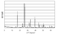
蛍光体の粉末X線回折図形は、CuKαの特性X線を用いた粉末X線回折法により測定した。測定装置としては、株式会社リガク製X線回折測定装置RINT2500TTR型を用いた。 The powder X-ray diffraction pattern of the phosphor was measured by a powder X-ray diffraction method using characteristic X-rays of CuKα. As a measuring apparatus, Rigaku X-ray diffraction measuring apparatus RINT2500TTR type was used.
比較例1
炭酸バリウム、酸化ユウロピウム、酸化スカンジウム、二酸化珪素の各原料をBa:Eu:Sc:Siのモル比が8.55:0.45:2:6となるように秤量し、アセトンを用いた湿式ボールミルにより4時間混合してスラリーを得た。得られたスラリーをエバポレーターにより乾燥後、得られた混合原料を、大気雰囲気中において1300℃の温度で6時間保持して焼成し、その後室温まで徐冷した。次いで、メノウ乳鉢による粉砕後、5体積%H2含有Ar雰囲気中で1300℃の温度で6時間保持して焼成し、その後室温まで徐冷して式(Ba0.95Eu0.05)9Sc2Si6O24で表される化合物からなる蛍光体1を得た。
Comparative Example 1
Wet ball mill using acetone by weighing each raw material of barium carbonate, europium oxide, scandium oxide and silicon dioxide so that the molar ratio of Ba: Eu: Sc: Si is 8.55: 0.45: 2: 6 For 4 hours to obtain a slurry. The obtained slurry was dried by an evaporator, and the obtained mixed raw material was baked by being held in an air atmosphere at a temperature of 1300 ° C. for 6 hours, and then gradually cooled to room temperature. Next, after pulverization with an agate mortar, it was fired in an Ar atmosphere containing 5% by volume of H 2 at a temperature of 1300 ° C. for 6 hours, and then gradually cooled to room temperature to obtain the formula (Ba 0.95 Eu 0.05 ) 9 Sc 2 Si 6 Phosphor 1 comprising a compound represented by O 24 was obtained.
蛍光体1の発光特性(励起スペクトル、発光スペクトル)を評価したところ、蛍光体1は、350nm以上480nm以下の波長の光により励起され、波長510nmに最大発光強度を有する発光を示すことがわかった。 When the emission characteristics (excitation spectrum, emission spectrum) of the phosphor 1 were evaluated, it was found that the phosphor 1 was excited by light having a wavelength of 350 nm or more and 480 nm or less and showed light emission having a maximum emission intensity at a wavelength of 510 nm. .
実施例1
比較例1と同様の混合原料を、大気雰囲気中において1300℃の温度で6時間保持して焼成し、その後室温まで徐冷した。次いで、メノウ乳鉢による粉砕後、アンモニア雰囲気中で1300℃の温度で6時間保持して焼成し、その後室温まで除冷した。次いで、メノウ乳鉢による粉砕後、再度アンモニア雰囲気中で1300℃の温度で6時間保持して焼成し、その後室温まで除冷して、式(Ba0.95Eu0.05)9Sc2Si6O21N2で表される化合物からなる蛍光体2を得た。
Example 1
A mixed raw material similar to that in Comparative Example 1 was baked by being held in an air atmosphere at a temperature of 1300 ° C. for 6 hours, and then gradually cooled to room temperature. Next, after pulverization with an agate mortar, the mixture was calcined in an ammonia atmosphere at a temperature of 1300 ° C. for 6 hours and then cooled to room temperature. Next, after pulverization with an agate mortar, it is fired again in an ammonia atmosphere at a temperature of 1300 ° C. for 6 hours, and then cooled to room temperature to obtain the formula (Ba 0.95 Eu 0.05 ) 9 Sc 2 Si 6 O 21 N 2. A phosphor 2 comprising the compound represented by the formula:
蛍光体2の励起スペクトルおよび発光スペクトルより、実施例1は350nm以上480nm以下の波長の光により励起され、波長570nmに最大発光強度を有する発光を示すことがわかった。 From the excitation spectrum and emission spectrum of phosphor 2, it was found that Example 1 was excited by light having a wavelength of 350 nm or more and 480 nm or less, and emitted light having a maximum emission intensity at a wavelength of 570 nm.
上記のように、本発明の蛍光体を発光装置に用いれば、発光の波長を長くすることもでき、演色性などの発光特性をさらに改善することのできる発光装置を与え得る蛍光体となることがわかる。 As described above, when the phosphor of the present invention is used in a light emitting device, the wavelength of light emission can be lengthened, and the phosphor can provide a light emitting device capable of further improving the light emission characteristics such as color rendering properties. I understand.
Claims (14)
aM1O・3M2O・6M3O2 (1)
(ここで、M1はBa、SrおよびCaからなる群より選ばれる1種以上のアルカリ土類金属元素を表し、M2はMgおよびZnからなる群より選ばれる1種以上の二価金属元素を表し、M3は四価金属元素を表し、aは3以上9以下の範囲の値である。) In the compound represented by the following formula (1), at least a part of M 2 is substituted with M 4 (M 4 represents a trivalent cation element), and a part of O in the compound is M 5 (M 5 Represents a trivalent anion element), and a phosphor obtained by substituting a part of M 1 and / or M 2 in the compound with an activating element.
aM 1 O · 3M 2 O · 6M 3 O 2 (1)
(Here, M 1 represents one or more alkaline earth metal elements selected from the group consisting of Ba, Sr and Ca, and M 2 represents one or more divalent metal elements selected from the group consisting of Mg and Zn. M 3 represents a tetravalent metal element, and a is a value in the range of 3 to 9.
M1 9(M2 3-1.5xM4 x)M3 6O24-1.5yM5 y (2)
(ここで、M1、M2、M3、M4およびM5は、それぞれ前記と同じ意味を有し、xは0を超え2以下の範囲の値であり、yは0を超え2以下の範囲の値である。) A phosphor in which a part of M 1 and / or M 2 in a compound represented by the following formula (2) is substituted with an activating element.
M 1 9 (M 2 3-1.5x M 4 x ) M 3 6 O 24-1.5y M 5 y (2)
(Here, M 1 , M 2 , M 3 , M 4 and M 5 each have the same meaning as described above, x is a value in the range of more than 0 and 2 or less, and y is more than 0 and 2 or less. Value in the range.)
Priority Applications (6)
| Application Number | Priority Date | Filing Date | Title |
|---|---|---|---|
| JP2008071109A JP2009227701A (en) | 2008-03-19 | 2008-03-19 | Phosphor and method for producing it |
| KR1020107021004A KR20100125343A (en) | 2008-03-19 | 2009-03-18 | Fluorophores and manufacturing method thereof |
| TW098108755A TW201005074A (en) | 2008-03-19 | 2009-03-18 | Phosphor and method for producing the same |
| CN200980109380XA CN101978023A (en) | 2008-03-19 | 2009-03-18 | Fluorophores and manufacturing method thereof |
| US12/933,335 US20110018426A1 (en) | 2008-03-19 | 2009-03-18 | Fluorophores and manufacturing method thereof |
| PCT/JP2009/055268 WO2009116567A1 (en) | 2008-03-19 | 2009-03-18 | Fluorophores and manufacturing method thereof |
Applications Claiming Priority (1)
| Application Number | Priority Date | Filing Date | Title |
|---|---|---|---|
| JP2008071109A JP2009227701A (en) | 2008-03-19 | 2008-03-19 | Phosphor and method for producing it |
Publications (1)
| Publication Number | Publication Date |
|---|---|
| JP2009227701A true JP2009227701A (en) | 2009-10-08 |
Family
ID=41090966
Family Applications (1)
| Application Number | Title | Priority Date | Filing Date |
|---|---|---|---|
| JP2008071109A Pending JP2009227701A (en) | 2008-03-19 | 2008-03-19 | Phosphor and method for producing it |
Country Status (6)
| Country | Link |
|---|---|
| US (1) | US20110018426A1 (en) |
| JP (1) | JP2009227701A (en) |
| KR (1) | KR20100125343A (en) |
| CN (1) | CN101978023A (en) |
| TW (1) | TW201005074A (en) |
| WO (1) | WO2009116567A1 (en) |
Families Citing this family (3)
| Publication number | Priority date | Publication date | Assignee | Title |
|---|---|---|---|---|
| CN104059658B (en) * | 2013-03-20 | 2015-10-28 | 海洋王照明科技股份有限公司 | Gadolinium acid calcium luminescent material of doping In and/or Sn and preparation method thereof |
| US10478556B2 (en) * | 2016-03-04 | 2019-11-19 | Roche Diabetes Care, Inc. | Probability based controller gain |
| US10600846B1 (en) * | 2018-09-13 | 2020-03-24 | Innolux Corporation | Electronic device |
Citations (2)
| Publication number | Priority date | Publication date | Assignee | Title |
|---|---|---|---|---|
| JP2006299259A (en) * | 2005-04-15 | 2006-11-02 | Patent Treuhand Ges Elektr Gluehlamp Mbh | Blue to yellow-orange light emitting phosphor, and light source having such a phosphor |
| JP2007077307A (en) * | 2005-09-15 | 2007-03-29 | Niigata Univ | Phosphor |
Family Cites Families (2)
| Publication number | Priority date | Publication date | Assignee | Title |
|---|---|---|---|---|
| US6045721A (en) * | 1997-12-23 | 2000-04-04 | Patent-Treuhand-Gesellschaft Fur Elekrische Gluhlampen Mbh | Barium magnesium aluminate phosphor |
| KR100887489B1 (en) * | 2004-04-27 | 2009-03-10 | 파나소닉 주식회사 | Phosphor composition and method for producing the same, and light-emitting device using the same |
-
2008
- 2008-03-19 JP JP2008071109A patent/JP2009227701A/en active Pending
-
2009
- 2009-03-18 CN CN200980109380XA patent/CN101978023A/en active Pending
- 2009-03-18 TW TW098108755A patent/TW201005074A/en unknown
- 2009-03-18 WO PCT/JP2009/055268 patent/WO2009116567A1/en active Application Filing
- 2009-03-18 US US12/933,335 patent/US20110018426A1/en not_active Abandoned
- 2009-03-18 KR KR1020107021004A patent/KR20100125343A/en not_active Application Discontinuation
Patent Citations (2)
| Publication number | Priority date | Publication date | Assignee | Title |
|---|---|---|---|---|
| JP2006299259A (en) * | 2005-04-15 | 2006-11-02 | Patent Treuhand Ges Elektr Gluehlamp Mbh | Blue to yellow-orange light emitting phosphor, and light source having such a phosphor |
| JP2007077307A (en) * | 2005-09-15 | 2007-03-29 | Niigata Univ | Phosphor |
Also Published As
| Publication number | Publication date |
|---|---|
| KR20100125343A (en) | 2010-11-30 |
| TW201005074A (en) | 2010-02-01 |
| WO2009116567A1 (en) | 2009-09-24 |
| CN101978023A (en) | 2011-02-16 |
| US20110018426A1 (en) | 2011-01-27 |
Similar Documents
| Publication | Publication Date | Title |
|---|---|---|
| JP4966530B2 (en) | Phosphor | |
| US7229571B2 (en) | Phosphor for white LED and a white LED | |
| JP5234781B2 (en) | Phosphor, method for producing the same, and light emitting device | |
| JP5224439B2 (en) | Phosphor and light emitting device using the same | |
| KR101172143B1 (en) | OXYNITRIDE-BASED PHOSPHORS COMPOSING OF SiON ELEMENT FOR WHITE LEDs, MANUFACTURING METHOD THEREOF AND LEDs USING THE SAME | |
| WO2006016711A1 (en) | Phosphor, method for producing same and light-emitting device | |
| JPWO2008084848A1 (en) | Phosphor, method for producing the same, and light emitting device | |
| US20140008680A1 (en) | Sialon phosphor, method for producing same, and light-emitting device package using same | |
| JP2009503183A (en) | Yellow phosphor and white light emitting device including the same | |
| JP2006232906A (en) | Fluorescent substance and light-emitting apparatus using the same | |
| JP2016216711A (en) | Phosphor, production method of the same, lighting apparatus and image display device | |
| US20110291142A1 (en) | Oxynitride phosphor, method for preparing the same, and light-emitting device | |
| JP2007254517A (en) | Composite oxide for phosphor and phosphor | |
| WO2012074102A1 (en) | Method for producing crystalline material | |
| JP5071709B2 (en) | Phosphors and light emitting devices | |
| JP5187817B2 (en) | Phosphors and light emitting devices | |
| WO2009116567A1 (en) | Fluorophores and manufacturing method thereof | |
| JP5881176B2 (en) | Phosphor, lighting apparatus and image display device | |
| JP2009108223A (en) | Phosphor, method for producing the same and light emitting apparatus using the same | |
| KR101162063B1 (en) | Green emitting phosphor for vacuum ultraviolet excited light emitting device, preparation method thereof and light emitting device having the same | |
| CN110317608B (en) | Blue light-emitting phosphor, blue light-emitting phosphor composition, light-emitting element, light-emitting device, and white light-emitting device | |
| JP5712428B2 (en) | Red phosphor for ultraviolet excitation light source | |
| KR100571882B1 (en) | Yellow phospher and white light emitting device comprising it | |
| JP7144002B2 (en) | Phosphor, phosphor composition using the same, and light-emitting device, lighting device, and image display device using the same | |
| JP7318924B2 (en) | Phosphor and light-emitting device using the same |
Legal Events
| Date | Code | Title | Description |
|---|---|---|---|
| A621 | Written request for application examination |
Free format text: JAPANESE INTERMEDIATE CODE: A621 Effective date: 20110207 |
|
| RD03 | Notification of appointment of power of attorney |
Free format text: JAPANESE INTERMEDIATE CODE: A7423 Effective date: 20111212 |
|
| A131 | Notification of reasons for refusal |
Free format text: JAPANESE INTERMEDIATE CODE: A131 Effective date: 20130507 |
|
| A02 | Decision of refusal |
Free format text: JAPANESE INTERMEDIATE CODE: A02 Effective date: 20130917 |