JP2009105068A - Electro-optical device, method for manufacturing electro-optical device and electronic equipment - Google Patents
Electro-optical device, method for manufacturing electro-optical device and electronic equipment Download PDFInfo
- Publication number
- JP2009105068A JP2009105068A JP2009027076A JP2009027076A JP2009105068A JP 2009105068 A JP2009105068 A JP 2009105068A JP 2009027076 A JP2009027076 A JP 2009027076A JP 2009027076 A JP2009027076 A JP 2009027076A JP 2009105068 A JP2009105068 A JP 2009105068A
- Authority
- JP
- Japan
- Prior art keywords
- conductive layer
- layer
- electro
- optical device
- conductive
- Prior art date
- Legal status (The legal status is an assumption and is not a legal conclusion. Google has not performed a legal analysis and makes no representation as to the accuracy of the status listed.)
- Withdrawn
Links
- 238000004519 manufacturing process Methods 0.000 title claims abstract description 29
- 238000000034 method Methods 0.000 title abstract description 32
- 239000010410 layer Substances 0.000 claims description 450
- 239000000758 substrate Substances 0.000 claims description 51
- 239000000463 material Substances 0.000 claims description 38
- VYPSYNLAJGMNEJ-UHFFFAOYSA-N Silicium dioxide Chemical compound O=[Si]=O VYPSYNLAJGMNEJ-UHFFFAOYSA-N 0.000 claims description 37
- 239000010936 titanium Substances 0.000 claims description 36
- 239000010949 copper Substances 0.000 claims description 28
- 239000011241 protective layer Substances 0.000 claims description 24
- PXHVJJICTQNCMI-UHFFFAOYSA-N Nickel Chemical compound [Ni] PXHVJJICTQNCMI-UHFFFAOYSA-N 0.000 claims description 18
- RTAQQCXQSZGOHL-UHFFFAOYSA-N Titanium Chemical compound [Ti] RTAQQCXQSZGOHL-UHFFFAOYSA-N 0.000 claims description 18
- BASFCYQUMIYNBI-UHFFFAOYSA-N platinum Chemical compound [Pt] BASFCYQUMIYNBI-UHFFFAOYSA-N 0.000 claims description 18
- 235000012239 silicon dioxide Nutrition 0.000 claims description 18
- 239000000377 silicon dioxide Substances 0.000 claims description 18
- 229910052719 titanium Inorganic materials 0.000 claims description 18
- 229910045601 alloy Inorganic materials 0.000 claims description 17
- 239000000956 alloy Substances 0.000 claims description 17
- 229910021332 silicide Inorganic materials 0.000 claims description 17
- RYGMFSIKBFXOCR-UHFFFAOYSA-N Copper Chemical compound [Cu] RYGMFSIKBFXOCR-UHFFFAOYSA-N 0.000 claims description 14
- 229910052802 copper Inorganic materials 0.000 claims description 14
- 229910052782 aluminium Inorganic materials 0.000 claims description 13
- XAGFODPZIPBFFR-UHFFFAOYSA-N aluminium Chemical compound [Al] XAGFODPZIPBFFR-UHFFFAOYSA-N 0.000 claims description 13
- ZOKXTWBITQBERF-UHFFFAOYSA-N Molybdenum Chemical compound [Mo] ZOKXTWBITQBERF-UHFFFAOYSA-N 0.000 claims description 12
- 229910052750 molybdenum Inorganic materials 0.000 claims description 12
- 239000011733 molybdenum Substances 0.000 claims description 12
- 229910052715 tantalum Inorganic materials 0.000 claims description 12
- GUVRBAGPIYLISA-UHFFFAOYSA-N tantalum atom Chemical compound [Ta] GUVRBAGPIYLISA-UHFFFAOYSA-N 0.000 claims description 12
- WFKWXMTUELFFGS-UHFFFAOYSA-N tungsten Chemical compound [W] WFKWXMTUELFFGS-UHFFFAOYSA-N 0.000 claims description 12
- 229910052721 tungsten Inorganic materials 0.000 claims description 12
- 239000010937 tungsten Substances 0.000 claims description 12
- 230000015572 biosynthetic process Effects 0.000 claims description 11
- 238000004544 sputter deposition Methods 0.000 claims description 11
- NRTOMJZYCJJWKI-UHFFFAOYSA-N Titanium nitride Chemical compound [Ti]#N NRTOMJZYCJJWKI-UHFFFAOYSA-N 0.000 claims description 9
- 229910052751 metal Inorganic materials 0.000 claims description 9
- 239000002184 metal Substances 0.000 claims description 9
- 229910052759 nickel Inorganic materials 0.000 claims description 6
- 229910052697 platinum Inorganic materials 0.000 claims description 6
- FVBUAEGBCNSCDD-UHFFFAOYSA-N silicide(4-) Chemical compound [Si-4] FVBUAEGBCNSCDD-UHFFFAOYSA-N 0.000 claims description 4
- 238000005520 cutting process Methods 0.000 claims description 3
- VSZWPYCFIRKVQL-UHFFFAOYSA-N selanylidenegallium;selenium Chemical compound [Se].[Se]=[Ga].[Se]=[Ga] VSZWPYCFIRKVQL-UHFFFAOYSA-N 0.000 claims description 3
- LEONUFNNVUYDNQ-UHFFFAOYSA-N vanadium atom Chemical compound [V] LEONUFNNVUYDNQ-UHFFFAOYSA-N 0.000 claims description 3
- 230000000452 restraining effect Effects 0.000 abstract 1
- 239000010408 film Substances 0.000 description 133
- 239000011229 interlayer Substances 0.000 description 42
- XUIMIQQOPSSXEZ-UHFFFAOYSA-N Silicon Chemical compound [Si] XUIMIQQOPSSXEZ-UHFFFAOYSA-N 0.000 description 35
- 229910052710 silicon Inorganic materials 0.000 description 35
- 239000010703 silicon Substances 0.000 description 35
- 239000010409 thin film Substances 0.000 description 30
- 238000002347 injection Methods 0.000 description 29
- 239000007924 injection Substances 0.000 description 29
- 238000007789 sealing Methods 0.000 description 19
- 229910004298 SiO 2 Inorganic materials 0.000 description 17
- 239000011521 glass Substances 0.000 description 17
- 239000004020 conductor Substances 0.000 description 13
- 239000012780 transparent material Substances 0.000 description 11
- 230000007274 generation of a signal involved in cell-cell signaling Effects 0.000 description 10
- 229910003437 indium oxide Inorganic materials 0.000 description 9
- PJXISJQVUVHSOJ-UHFFFAOYSA-N indium(iii) oxide Chemical compound [O-2].[O-2].[O-2].[In+3].[In+3] PJXISJQVUVHSOJ-UHFFFAOYSA-N 0.000 description 9
- 238000010586 diagram Methods 0.000 description 7
- 229910052581 Si3N4 Inorganic materials 0.000 description 6
- 239000011651 chromium Substances 0.000 description 6
- 238000001312 dry etching Methods 0.000 description 6
- 238000009832 plasma treatment Methods 0.000 description 6
- HQVNEWCFYHHQES-UHFFFAOYSA-N silicon nitride Chemical compound N12[Si]34N5[Si]62N3[Si]51N64 HQVNEWCFYHHQES-UHFFFAOYSA-N 0.000 description 6
- 238000007740 vapor deposition Methods 0.000 description 5
- VYZAMTAEIAYCRO-UHFFFAOYSA-N Chromium Chemical compound [Cr] VYZAMTAEIAYCRO-UHFFFAOYSA-N 0.000 description 4
- 239000003990 capacitor Substances 0.000 description 4
- 238000005229 chemical vapour deposition Methods 0.000 description 4
- 238000001035 drying Methods 0.000 description 4
- 229910021420 polycrystalline silicon Inorganic materials 0.000 description 4
- 229920001721 polyimide Polymers 0.000 description 4
- 239000000853 adhesive Substances 0.000 description 3
- 230000001070 adhesive effect Effects 0.000 description 3
- 230000002950 deficient Effects 0.000 description 3
- 230000000694 effects Effects 0.000 description 3
- 238000010438 heat treatment Methods 0.000 description 3
- 229910010272 inorganic material Inorganic materials 0.000 description 3
- 239000011147 inorganic material Substances 0.000 description 3
- 238000009413 insulation Methods 0.000 description 3
- 239000007788 liquid Substances 0.000 description 3
- 239000000203 mixture Substances 0.000 description 3
- 230000003071 parasitic effect Effects 0.000 description 3
- 230000002093 peripheral effect Effects 0.000 description 3
- 229910052698 phosphorus Inorganic materials 0.000 description 3
- 239000011574 phosphorus Substances 0.000 description 3
- -1 phosphorus ions Chemical class 0.000 description 3
- 238000005268 plasma chemical vapour deposition Methods 0.000 description 3
- 239000004925 Acrylic resin Substances 0.000 description 2
- 229920000178 Acrylic resin Polymers 0.000 description 2
- 239000004642 Polyimide Substances 0.000 description 2
- 229910010413 TiO 2 Inorganic materials 0.000 description 2
- QVGXLLKOCUKJST-UHFFFAOYSA-N atomic oxygen Chemical compound [O] QVGXLLKOCUKJST-UHFFFAOYSA-N 0.000 description 2
- 229910052804 chromium Inorganic materials 0.000 description 2
- 239000013256 coordination polymer Substances 0.000 description 2
- 239000013078 crystal Substances 0.000 description 2
- 230000003247 decreasing effect Effects 0.000 description 2
- 239000003822 epoxy resin Substances 0.000 description 2
- 238000005530 etching Methods 0.000 description 2
- 239000010931 gold Substances 0.000 description 2
- 239000011810 insulating material Substances 0.000 description 2
- 238000005468 ion implantation Methods 0.000 description 2
- 239000004973 liquid crystal related substance Substances 0.000 description 2
- 239000011159 matrix material Substances 0.000 description 2
- 239000011368 organic material Substances 0.000 description 2
- 230000003647 oxidation Effects 0.000 description 2
- 238000007254 oxidation reaction Methods 0.000 description 2
- 239000001301 oxygen Substances 0.000 description 2
- 229910052760 oxygen Inorganic materials 0.000 description 2
- 238000005192 partition Methods 0.000 description 2
- 238000000059 patterning Methods 0.000 description 2
- 238000000206 photolithography Methods 0.000 description 2
- 230000000704 physical effect Effects 0.000 description 2
- 238000005498 polishing Methods 0.000 description 2
- 229920000647 polyepoxide Polymers 0.000 description 2
- 239000009719 polyimide resin Substances 0.000 description 2
- 239000011347 resin Substances 0.000 description 2
- 229920005989 resin Polymers 0.000 description 2
- LIVNPJMFVYWSIS-UHFFFAOYSA-N silicon monoxide Chemical compound [Si-]#[O+] LIVNPJMFVYWSIS-UHFFFAOYSA-N 0.000 description 2
- BQCADISMDOOEFD-UHFFFAOYSA-N Silver Chemical compound [Ag] BQCADISMDOOEFD-UHFFFAOYSA-N 0.000 description 1
- 238000010521 absorption reaction Methods 0.000 description 1
- 229910021417 amorphous silicon Inorganic materials 0.000 description 1
- 239000012300 argon atmosphere Substances 0.000 description 1
- 238000004380 ashing Methods 0.000 description 1
- 239000012298 atmosphere Substances 0.000 description 1
- 238000006243 chemical reaction Methods 0.000 description 1
- 230000007423 decrease Effects 0.000 description 1
- 230000002542 deteriorative effect Effects 0.000 description 1
- 238000009792 diffusion process Methods 0.000 description 1
- 238000007599 discharging Methods 0.000 description 1
- 239000007789 gas Substances 0.000 description 1
- PCHJSUWPFVWCPO-UHFFFAOYSA-N gold Chemical compound [Au] PCHJSUWPFVWCPO-UHFFFAOYSA-N 0.000 description 1
- 229910052737 gold Inorganic materials 0.000 description 1
- 239000011261 inert gas Substances 0.000 description 1
- 238000010030 laminating Methods 0.000 description 1
- 238000005224 laser annealing Methods 0.000 description 1
- 239000012299 nitrogen atmosphere Substances 0.000 description 1
- 229920005591 polysilicon Polymers 0.000 description 1
- 239000012495 reaction gas Substances 0.000 description 1
- 239000004065 semiconductor Substances 0.000 description 1
- 229910052814 silicon oxide Inorganic materials 0.000 description 1
- 229910052709 silver Inorganic materials 0.000 description 1
- 239000004332 silver Substances 0.000 description 1
- 239000002356 single layer Substances 0.000 description 1
- 239000000126 substance Substances 0.000 description 1
- 238000001771 vacuum deposition Methods 0.000 description 1
Images


Landscapes
- Electroluminescent Light Sources (AREA)
Abstract
Description
本発明は、電気光学装置及び電気光学装置の製造方法に関するものである。 The present invention relates to an electro-optical device and a method for manufacturing the electro-optical device.
液晶素子、有機EL素子、電気泳動素子、電子放出素子等といった電気光学素子を複数備えた表示ディスプレイの駆動方式の一つにアクティブマトリクス駆動方式がある。アクティブマトリクス駆動方式の表示ディスプレイには、例えば、各電気光学素子の陰極が透明電極で形成され、その陰極側から有機EL素子にて発せられた光が出射されるトップエミッションタイプの表示ディスプレイがある。 There is an active matrix driving method as one of driving methods of a display display including a plurality of electro-optical elements such as a liquid crystal element, an organic EL element, an electrophoretic element, and an electron emitting element. Examples of the active matrix driving display include a top emission type display in which the cathode of each electro-optic element is formed of a transparent electrode, and light emitted from the organic EL element is emitted from the cathode side. .
この種の表示ディスプレイにおいては、透明電極はスズドープ酸化インジウム(ITO)で構成された透明導電性薄膜であって表示パネル部の全面に渡って形成されている。一般に、透明導電性薄膜は金属と比較してその抵抗率が高いことが知られている。従って、表示パネル上に形成される位置によって電気光学素子の陰極の電位に差が生じる。その結果、例えば、全ての画素に同じ電圧レベルのデータ信号を供給したとき、画素が形成される位置によって輝度に差が生じてしまう。この結果、表示パネル部に、所謂、表示ムラが生じる。特に表示パネル部が大型化されるのに伴ってこの表示ムラが顕著に現れてしまう。 In this type of display, the transparent electrode is a transparent conductive thin film made of tin-doped indium oxide (ITO) and is formed over the entire surface of the display panel. In general, it is known that a transparent conductive thin film has a higher resistivity than a metal. Accordingly, the potential of the cathode of the electro-optic element varies depending on the position formed on the display panel. As a result, for example, when data signals having the same voltage level are supplied to all the pixels, a difference in luminance occurs depending on the position where the pixels are formed. As a result, so-called display unevenness occurs in the display panel unit. In particular, this display unevenness appears remarkably as the display panel is enlarged.
例えば、表示パネル部の中央部に形成される画素の有機EL素子OLEDの陰極の電位が外周部に形成される画素の有機EL素子OLEDの陰極の電位に比べて高くなってしまう場合がある。この結果、表示パネル部の中央部と外周部とで表示ムラが生じる。 For example, the potential of the cathode of the organic EL element OLED of the pixel formed in the central part of the display panel unit may be higher than the potential of the cathode of the organic EL element OLED of the pixel formed in the outer peripheral part. As a result, display unevenness occurs between the central portion and the outer peripheral portion of the display panel portion.
そこで、表示パネル部の陽極側である基板上に導電性の突起部を設け、その突起部を有機EL素子の陰極に接続された透明導電性薄膜に接続するようにした構造を備えた表示ディスプレイが知られている(例えば、特許文献1参照)。このようにすることで、有機EL素子OLEDの陰極の電位が、各画素を形成される位置によって差が生じるのを抑制することができる。 Therefore, a display having a structure in which a conductive protrusion is provided on the substrate on the anode side of the display panel and the protrusion is connected to a transparent conductive thin film connected to the cathode of the organic EL element. Is known (see, for example, Patent Document 1). By doing in this way, it can suppress that the potential of the cathode of organic EL element OLED produces a difference by the position in which each pixel is formed.
しかしながら、前記したような導電性の突起部を形成することは技術的に困難である。本発明は上記問題点を解消するためになされたものであって、表示ムラの発生を抑制することで表示品位を向上するようにした電気光学装置、電気光学装置の製造方法及び電子機器を提供することにある。 However, it is technically difficult to form the conductive protrusions as described above. The present invention has been made to solve the above problems, and provides an electro-optical device, a method for manufacturing the electro-optical device, and an electronic apparatus that improve display quality by suppressing the occurrence of display unevenness. There is to do.
本発明の電気光学装置は、基板上に、陽極と、該陽極に対向する位置に形成された陰極と、前記陽極と前記陰極との間に設けられた発光性材料とを備え、前記陽極は前記発光性材料が設けられる画素毎に形成された電気光学装置において、前記基板と前記陽極との間に形成された導電層と、前記陰極と前記導電層とを電気的に接続するための接続部とを備えている。 An electro-optical device of the present invention includes an anode, a cathode formed at a position facing the anode, and a luminescent material provided between the anode and the cathode on a substrate, In the electro-optical device formed for each pixel provided with the light emitting material, a conductive layer formed between the substrate and the anode, and a connection for electrically connecting the cathode and the conductive layer Department.
これによれば、接続部を介して前記陰極と前記導電層と電気的に接続した。従って、前記陰極が、例えば、スズドープ酸化インジウム(ITO)といった比較的抵抗率が高い透明導電性薄膜であっても前記陰極の電位が画素毎で異なることはない。この結果、画素が形成される位置によって表示ムラが発生するのを抑制することができる。このことから、表示品位が優れた電気光学装置を提供することができる。 According to this, the said cathode and the said conductive layer were electrically connected through the connection part. Therefore, even if the cathode is a transparent conductive thin film having a relatively high resistivity, such as tin-doped indium oxide (ITO), the potential of the cathode does not vary from pixel to pixel. As a result, it is possible to suppress display unevenness depending on the position where the pixel is formed. Thus, an electro-optical device with excellent display quality can be provided.
この電気光学装置において、前記接続部は前記画素毎に備えられていてもよい。
これによれば、形成される位置によって表示ムラが発生するのを画素毎に確実に抑制することができる。
In this electro-optical device, the connection portion may be provided for each pixel.
According to this, it is possible to reliably suppress the occurrence of display unevenness for each pixel depending on the position where it is formed.
この電気光学装置において、前記接続部はコンタクトホールで構成されていてもよい。
これによれば、前記接続部を容易に形成することができる。
In this electro-optical device, the connection portion may be formed of a contact hole.
According to this, the said connection part can be formed easily.
この電気光学装置において、前記基板上には前記発光性材料に供給される電流を制御するための能動素子が形成される素子形成層を備え、前記素子形成層と前記導電層との間には前記素子形成層と前記導電層とを電気的に切断するための絶縁層が形成されていてもよい。 In this electro-optical device, an element forming layer in which an active element for controlling a current supplied to the light emitting material is formed on the substrate is provided, and the element forming layer and the conductive layer are interposed between the element forming layer and the conductive layer. An insulating layer for electrically cutting the element formation layer and the conductive layer may be formed.
これによれば、前記導電層の上方に前記能動素子を形成した電気光学装置において、画素が形成される位置によって表示ムラが発生するのを抑制することができる。 According to this, in the electro-optical device in which the active element is formed above the conductive layer, it is possible to suppress display unevenness depending on the position where the pixel is formed.
この電気光学装置において、前記絶縁層は、その誘電率をεとしたとき、膜厚が2ε/3.5μm以上であってもよい。
これによれば、絶縁層を、その膜厚が2ε/3.5μm以上になるように形成した。従って、絶縁層上に形成される前記能動素子に前記導電層を構成する材料が拡散するのを確実に防止することができる。また、前記導電層と前記能動素子の間に形成される寄生容量を低減し、駆動回路を安定動作させることができ、それによって電気光学装置の表示品質を向上させることができる。
In this electro-optical device, the insulating layer may have a thickness of 2ε / 3.5 μm or more, where ε is a dielectric constant.
According to this, the insulating layer was formed so that the film thickness was 2ε / 3.5 μm or more. Therefore, it is possible to reliably prevent the material constituting the conductive layer from diffusing into the active element formed on the insulating layer. Further, the parasitic capacitance formed between the conductive layer and the active element can be reduced, and the drive circuit can be stably operated, thereby improving the display quality of the electro-optical device.
この電気光学装置において、前記導電層はチタン(Ti)、タンタル(Ta)、タングステン(W)、モリブデン(Mo)、バナジウム(V)、ジルコニウム(Zr)、及びこれらの合金またはシリサイドのうちの一つで構成されていてもよい。
これによれば、導電層を容易に形成することができる。
In this electro-optical device, the conductive layer is made of titanium (Ti), tantalum (Ta), tungsten (W), molybdenum (Mo), vanadium (V), zirconium (Zr), and an alloy or silicide thereof. It may be composed of two.
According to this, a conductive layer can be formed easily.
この電気光学装置において、前記導電層は少なくとも一層の金属層を含む複数の導電層から構成されていてもよい。 In this electro-optical device, the conductive layer may include a plurality of conductive layers including at least one metal layer.
これによれば、例えば、導電層のうち他の層に接して形成される導電層を、該導電層が構成される材料が拡散されにくいもので構成することで前記他の層の物性を変化させないようにすることができる。 According to this, for example, a conductive layer formed in contact with another layer among the conductive layers is made of a material in which the material constituting the conductive layer is difficult to diffuse, thereby changing the physical properties of the other layer. You can avoid it.
この電気光学装置において、前記基板上に該基板を保護する下地保護層を備え、その下地保護層は二酸化珪素で構成され、前記複数の導電層は前記下地保護層上から順に第1導電層、第2導電層から構成される導電層であって、前記第1導電層はチタン(Ti)、タンタル(Ta)、タングステン(W)、モリブデン(Mo)、及びこれらの合金またはシリサイドのいずれか一つで構成され、前記第2導電層はアルミニウム(A1)、ニッケル(Ni)及び白金(Pt)、及びこれらの合金またはシリサイドのいずれか一つで構成されていてもよい。
これによれば、前記保護層との密着性に優れ且つ導電率の低い導電層を備えた電気光学装置を提供することができる。
In this electro-optical device, the substrate includes a base protective layer that protects the substrate, the base protective layer is made of silicon dioxide, and the plurality of conductive layers are first conductive layers in order from the base protective layer, A conductive layer composed of a second conductive layer, wherein the first conductive layer is one of titanium (Ti), tantalum (Ta), tungsten (W), molybdenum (Mo), and alloys or silicides thereof. The second conductive layer may be made of any one of aluminum (A1), nickel (Ni) and platinum (Pt), and alloys or silicides thereof.
According to this, it is possible to provide an electro-optical device provided with a conductive layer having excellent adhesion to the protective layer and low conductivity.
この電気光学装置において、前記基板上に該基板を保護する下地保護層を備え、その保護層は二酸化珪素で構成され、前記複数の導電層は前記下地保護層上から順に第1導電層、第2導電層、第3導電層から構成され、前記第1導電層はチタン(Ti)、タンタル(Ta)、タングステン(W)、モリブデン(Mo)、及びこれらの合金またはシリサイドのいずれか一つで構成され、前記第2導電層は銅(Cu)、アルミニウム(A1)、ニッケル(Ni)及び白金(Pt)、及びこれらの合金またはシリサイドのいずれか一つで構成され、前記第3導電層は窒化チタン(TiN)、チタン(Ti)、タンタル(Ta)、タングステン(W)、モリブデン(Mo)、及びこれらの合金またはシリサイドのいずれか一つで構成されていてもよい。 In this electro-optical device, a base protective layer for protecting the substrate is provided on the substrate, the protective layer is made of silicon dioxide, and the plurality of conductive layers are arranged in order from the base protective layer, the first conductive layer, The first conductive layer is composed of titanium (Ti), tantalum (Ta), tungsten (W), molybdenum (Mo), and an alloy or silicide thereof. The second conductive layer is made of copper (Cu), aluminum (A1), nickel (Ni), platinum (Pt), and any one of these alloys or silicides, and the third conductive layer is Titanium nitride (TiN), titanium (Ti), tantalum (Ta), tungsten (W), molybdenum (Mo), and alloys or silicides thereof may be used.
これによれば、チタン(Ti)で第1導電層を構成した。従って、第1導電層を下地保護層に密着して形成することができる。また、銅(Cu)で第2導電層を構成した。従って、導電層の導電率を高くすることができる。さらに、窒化チタン(TiN)で第3導電層を構成した。従って、第2導電層を構成する銅(Cu)と第3導電層上に形成される層を構成する材料とが反応して、その結果、第2導電層の導電率が低下するのを防止することができる。 According to this, the 1st conductive layer was comprised with titanium (Ti). Therefore, the first conductive layer can be formed in close contact with the base protective layer. Moreover, the 2nd conductive layer was comprised with copper (Cu). Accordingly, the conductivity of the conductive layer can be increased. Furthermore, the third conductive layer was composed of titanium nitride (TiN). Therefore, it is prevented that the copper (Cu) constituting the second conductive layer reacts with the material constituting the layer formed on the third conductive layer, and as a result, the conductivity of the second conductive layer is lowered. can do.
この電気光学装置において、前記導電層は前記基板から突出して形成された突出部を備えていてもよい。
これによれば、突出された導電層を各種外部装置と直接接続することで特別なインターフェースといった接続手段を設けることなく前記各陰極の電位を直接制御することができる。
In the electro-optical device, the conductive layer may include a protruding portion that protrudes from the substrate.
According to this, the potential of each cathode can be directly controlled without providing a connection means such as a special interface by directly connecting the protruding conductive layer to various external devices.
本発明の電気光学装置の製造方法は、基板上に、陽極と、該陽極に対向する位置に形成された陰極と、前記陽極と前記陰極との間に設けられた発光性材料とを備えるとともに、前記発光性材料を画素毎に区分けするためのバンク層と、前記基板と前記陽極との間に形成された導電層と、前記陰極と前記導電層とを電気的に接続するための接続部と、前記基板上には前記発光性材料に供給される電流を制御するための能動素子が形成される素子形成層と、前記素子形成層と前記導電層との間には前記素子形成層と前記導電層とを電気的に切断するための絶縁層とを備えた電気光学装置の製造方法において、前記基板の上方に前記導電層を形成する工程と、前記導電層の上方に前記絶縁層、前記素子形成層、前記陽極及びバンク層を形成する工程と、前記絶縁層に開口パターンを形成するのと同時に前記陰極と前記導電層とを電気的に接続するための接続部開口パターンを形成する工程と、前記発光性材料を形成する工程と、前記接続部を含む前記発光性材料を形成した領域の全面に透明性導電膜を形成する工程とを備えた。 An electro-optical device manufacturing method of the present invention includes an anode, a cathode formed at a position facing the anode, and a luminescent material provided between the anode and the cathode on a substrate. A bank layer for dividing the luminescent material into pixels, a conductive layer formed between the substrate and the anode, and a connection part for electrically connecting the cathode and the conductive layer. An element forming layer on which an active element for controlling a current supplied to the light emitting material is formed on the substrate; and the element forming layer between the element forming layer and the conductive layer; In an electro-optical device manufacturing method comprising an insulating layer for electrically cutting the conductive layer, the step of forming the conductive layer above the substrate, the insulating layer above the conductive layer, Forming the element forming layer, the anode, and the bank layer; Forming a connection portion opening pattern for electrically connecting the cathode and the conductive layer simultaneously with forming an opening pattern in the insulating layer, forming the luminescent material, and connecting Forming a transparent conductive film on the entire surface of the region including the light emitting material.
これによれば、前記陰極が、例えば、スズドープ酸化インジウム(ITO)といった比較的抵抗率が高い透明導電性薄膜であっても画素が形成される位置によって表示ムラが発生するのを抑制することができる電気光学装置を製造することができる。また、4層から6層ある絶縁層に開口部(コンタクトホール、画素発光領域など)を形成するのと同時に、前記陰極と前記導電層とを電気的に接続する接続部(コンタクトホール)を形成できるので、工程を変更せずに高品質な電気光学装置を製造することができる。 According to this, even if the cathode is a transparent conductive thin film having a relatively high resistivity such as tin-doped indium oxide (ITO), it is possible to suppress display unevenness depending on the position where the pixel is formed. An electro-optical device that can be manufactured can be manufactured. In addition, an opening (contact hole, pixel light-emitting region, etc.) is formed in four to six insulating layers, and at the same time, a connection portion (contact hole) for electrically connecting the cathode and the conductive layer is formed. Therefore, a high-quality electro-optical device can be manufactured without changing the process.
この電気光学装置の製造方法において、前記導電層は第1導電層、第2導電層及び第3導電層から構成される導電層を備え、前記素子形成層は前記能動素子に信号を供給するための第1の信号線と第2の信号線とを備え、前記第1導電層は前記第1の信号線を形成すると同時に形成され、前記第2導電層は前記第2の信号線を形成すると同時に形成されていてもよい。
これによれば、前記接続部を容易に形成することができる。
In the method of manufacturing the electro-optical device, the conductive layer includes a conductive layer including a first conductive layer, a second conductive layer, and a third conductive layer, and the element formation layer supplies a signal to the active element. A first signal line and a second signal line, wherein the first conductive layer is formed simultaneously with the formation of the first signal line, and the second conductive layer forms the second signal line. It may be formed at the same time.
According to this, the said connection part can be formed easily.
この電気光学装置の製造方法において、前記導電層はスパッタ法で形成するようにしてもよい。 In the method of manufacturing the electro-optical device, the conductive layer may be formed by a sputtering method.
これによれば、蒸着法といった他の方法で形成する場合と比較して前記導電層の成膜温度を低くすることができる。この結果、基板等に欠陥等が生じるのを防止することができる。 According to this, compared with the case where it forms by other methods, such as a vapor deposition method, the film-forming temperature of the said conductive layer can be made low. As a result, it is possible to prevent the substrate or the like from being defective.
本発明の電子機器は、上記電気光学装置を備えている。
これによれば、陰極が、例えば、スズドープ酸化インジウム(ITO)といった比較的抵抗率が高い透明導電性薄膜であっても表示品位が優れた電子機器を提供することができる。
The electronic apparatus of the present invention includes the electro-optical device.
According to this, even if the cathode is a transparent conductive thin film having a relatively high resistivity such as tin-doped indium oxide (ITO), an electronic device with excellent display quality can be provided.
以下、本発明を液晶表示装置に適用した各実施形態を図面に基づいて説明する。また、各実施形態は、本発明の一態様を示すものであり、この発明を限定するものではなく、本発明の技術思想の範囲内で任意に変更可能である。さらに、以下に示す各図においては、各層や各部材を図面上で認識可能な程度の大きさとするため、各層や各部材ごとに縮尺を異ならせてある。
(第1実施形態)
本発明を具体化した第1実施形態を図1〜図10に従って説明する。図1は、有機ELディスプレイの電気的構成を説明するためのブロック図である。図2は、表示パネル部及びデータ線駆動回路の電気的構成を示す回路図である。図3は、本実施形態における画素の回路図である。また、図4は本実施形態における表示パネル部の一部断面図である。
Embodiments in which the present invention is applied to a liquid crystal display device will be described below with reference to the drawings. Each embodiment shows one mode of the present invention, does not limit the present invention, and can be arbitrarily changed within the scope of the technical idea of the present invention. Furthermore, in each figure shown below, in order to make each layer and each member large enough to be recognized on the drawing, the scale is varied for each layer and each member.
(First embodiment)
1st Embodiment which actualized this invention is described according to FIGS. FIG. 1 is a block diagram for explaining an electrical configuration of an organic EL display. FIG. 2 is a circuit diagram showing an electrical configuration of the display panel unit and the data line driving circuit. FIG. 3 is a circuit diagram of a pixel in this embodiment. FIG. 4 is a partial cross-sectional view of the display panel unit in the present embodiment.
図1に示すように、有機ELディスプレイ10は、信号生成回路11、表示パネル部12、走査線駆動回路13及びデータ線駆動回路14を備えている。有機ELディスプレイ10の信号生成回路11、走査線駆動回路13及びデータ線駆動回路14は、それぞれが独立した電子部品によって構成されていてもよい。例えば、信号生成回路11、走査線駆動回路13及びデータ線駆動回路14が、各々1チップの半導体集積回路装置によって構成されていてもよい。また、信号生成回路11、走査線駆動回路13及びデータ線駆動回路14の全部若しくは一部がプログラマブルなICチップで構成され、その機能がICチップに書き込まれたプログラムによりソフトウェア的に実現されてもよい。
As shown in FIG. 1, the
信号生成回路11は、図示しない外部装置から供給されるクロックパルスCP及び画像デジタルデータDを入力する。信号生成回路11は、クロックパルスCPに基づいて水平同期信号HSYNC及び垂直同期信号VSYNCを作成する。
また、信号生成回路11は、その作成した水平同期信号HSYNCを走査線駆動回路13に出力するとともに、前記垂直同期信号VSYNCをデータ線駆動回路14に出力する。さらに、信号生成回路11は、画像デジタルデータDをデータ線駆動回路14に出力する。
The
The
表示パネル部12は、図2に示すように、行方向に沿って延設されるn本の走査線Y1,Y2,…,Ynを備えている。また、表示パネル部12は、列方向に沿って延設されるm本のデータ線X1,X2,…,Xmを備えている。走査線Y1,Y2,…,Ynは同表示パネル部12の図中上部側から下部側に向かって第1の走査線Y1、第2の走査線Y2、…、第nの走査線Ynの順に備えられている。そして、前記各走査線Y1,Y2,…,Ynと前記各データ線X1,X2,…,Xmとの交差部に対応した各位置には画素20が形成されている。
As shown in FIG. 2, the
さらに、表示パネル部12は、前記各データ線X1,X2,…,Xmに並行して延設されるm本の電源線Loを備えている。全ての電源線Loには電源電圧Voが供給されている。
Furthermore, the
各画素20は、対応する走査線Y1,Y2,…,Ynを介して走査線駆動回路13に接続されている。また、各画素20は、対応するデータ線X1,X2,…,Xmを介してデータ線駆動回路14に接続されている。さらに、各画素20は、電源線Loに接続されている。
Each
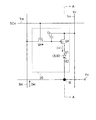
画素20は、その各々が図3に示すように、駆動トランジスタQd、スイッチングトランジスタQsw、保持キャパシタCo及び有機EL素子OLEDを備えている。尚、図3は、n番目の走査線Ynとm番目のデータ線Xmとの交差部に対応する位置に形成された画素20の等価回路図である。各画素20の電気的構成は全て同じであるので、説明の便宜上、以下、n番目の走査線Ynとm番目のデータ線Xmとの交差部に対応する位置に形成された画素20についてのみについて説明し、他の画素20についてはその説明を省略する。
Each of the
駆動トランジスタQdは、通常はTFT(薄膜トランジスタ)で構成されている。また、駆動トランジスタQdは本実施形態ではその導電型がP型である。スイッチングトランジスタQswは本実施形態ではその導電型がN型である。 The drive transistor Qd is usually composed of a TFT (Thin Film Transistor). The drive transistor Qd has a P-type conductivity in this embodiment. The conductivity type of the switching transistor Qsw is N-type in this embodiment.
スイッチングトランジスタQswは、そのソースがデータ線Xmに接続されている。スイッチングトランジスタQswのゲートは走査線Ynに接続されている。スイッチングトランジスタQswのドレインは、駆動トランジスタQdのゲートに接続されている。駆動トランジスタQdのゲート/ソース間には保持キャパシタCoが接続されている。また、駆動トランジスタQdのソースは電源線Loに接続されている。駆動トランジスタQdのドレインは有機EL素子OLEDの陽極E1に接続されている。 The source of the switching transistor Qsw is connected to the data line Xm. The gate of the switching transistor Qsw is connected to the scanning line Yn. The drain of the switching transistor Qsw is connected to the gate of the driving transistor Qd. A holding capacitor Co is connected between the gate and source of the driving transistor Qd. The source of the driving transistor Qd is connected to the power supply line Lo. The drain of the driving transistor Qd is connected to the anode E1 of the organic EL element OLED.
上記のように構成された画素20は、その有機EL素子OLEDの陰極E2がコンタクトホールHを介して他の有機EL素子と共通の陰極に電気的に接続されている。また、前記陰極E2は図示しない外部装置に接続するための接続ポートPoに接続されている。
In the
走査線駆動回路13は、走査信号SC1,SC2,…,SCnを作成する。各走査信号SC1,SC2,…,SCnはLレベル及びHレベルを有する電圧信号である。また、走査線駆動回路13は前記水平同期信号HSYNCに従って、Hレベルの走査信号を各走査線Y1,Y2,…,Ynに出力することで順次走査線Y1,Y2,…,Ynを選択駆動する。
The scanning
データ線駆動回路14は、図2に示すように複数の単一ラインドライバ14aを備えている。複数の単一ラインドライバ14aの各々は対応するデータ線X1,X2,…,Xmに接続されている。また、各単一ラインドライバ14aは、前記信号生成回路11から出力された画像デジタルデータDを入力する。そして、各単一ラインドライバ14aは、入力された画像デジタルデータDの大きさに対応したレベルのアナログ電圧信号であるデータ信号D1,D2,…,Dmを作成する。そして、単一ラインドライバ14aは、前記信号生成回路11から出力された垂直同期信号VSYNCに従って前記データ信号D1,D2,…,Dmを対応するデータ線X1,X2,…,Xmを介して各画素20に一斉に出力する。
As shown in FIG. 2, the data
そして、前記走査線駆動回路13が水平同期信号HSYNCに従って走査線Y1,Y2,…,Ynのうちの一本の走査線にHレベルの走査信号を出力すると、その走査線に接続された一行分の全ての画素20の各スイッチングトランジスタQswがオンになる。このとき、前記データ線駆動回路14の各単一ラインドライバ14aから対応するデータ線X1,X2,…,Xmを介してデータ信号D1,D2,…,Dmが一斉に出力される。すると、前記スイッチングトランジスタQswがオンになった前記一行分の全ての画素20の各保持キャパシタCoにデータ信号が供給される。この結果、前記各画素20は、このデータ信号に応じて同画素20の内部状態(保持キャパシタCoの電荷量)が設定され、これに応じて駆動トランジスタQdの導電率が制御される。この結果、その導電率に応じたレベルの駆動電流Ielが有機EL素子OLEDに供給され、有機EL素子OLEDが同駆動電流Ielの電流レベルに応じた輝度で発光する。
When the scanning
以降、各走査線Y1,Y2,…,Ynが順次選択されることで各画素20にデータ信号D1,D2,…,Dmが供給され、各有機EL素子OLEDが駆動電流Ielの電流レベルに応じた輝度で発光する。このようにすることで表示パネル部12上にデータ信号D1,D2,…,Dmに応じた画像が表示される。
Thereafter, the data signals D1, D2,..., Dm are supplied to the
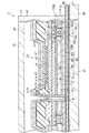
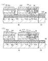
次に、表示パネル部12の構造について図4に従って説明する。図4は駆動トランジスタQdと有機EL素子OLEDとを含む表示パネル部12の一部断面図である。図4に示す断面図は、図3中のA−A線に沿う断面に対応している。
Next, the structure of the
図4に示すように、ガラス基板30上には二酸化珪素(SiO2)で構成された下地保護層31が形成されている。下地保護層31上には第1導電層M1が前記ガラス基板30のほぼ全面に形成されている。第1導電層M1は導電率が高く且つ下地保護層31との密着性に優れた材料で構成されている。本実施形態の第1導電層M1は、二酸化珪素(SiO2)との密着性に優れた金属であるチタン(Ti)で構成されている。また、第1導電層M1上には第2導電層M2が形成されている。
As shown in FIG. 4, a base
第2導電層M2は、導電率が高い材料で構成されている。本実施形態の第2導電層M2は銅(Cu)で構成されている。また、第2導電層M2上には第3導電層M3が形成されている。 The second conductive layer M2 is made of a material having high conductivity. The second conductive layer M2 of this embodiment is made of copper (Cu). A third conductive layer M3 is formed on the second conductive layer M2.
第3導電層M3は、導電率が高く且つ前記第2導電層M2を構成する材料が第3導電層M3上に形成される下地絶縁膜32に拡散するのを抑制する材料で構成されている。第3導電層M3を第2導電層M2と下地絶縁膜32との間に形成することで、第2導電層M2を構成する材料と下地絶縁膜32を構成する材料とが反応して、その結果、第2導電層M2の物性が変化してその導電率が低下する若しくは下地絶縁膜32の絶縁性が低下するのを防止することができる。本実施形態の第3導電層M3は、二酸化珪素(SiO2)に拡散しにくい金属である窒化チタン(TiN)で構成されている。そして、本実施形態では前記第1〜第3導電層M1,M2,M3で導電層MLが構成されている。
The third conductive layer M3 is made of a material having high conductivity and suppressing diffusion of the material constituting the second conductive layer M2 into the
また、この導電層MLは、その一端(図中右側)が外方に突出されている。この突出した部分の導電層MLが前記接続ポートPoに対応している。
前記第3導電層M3上にはコンタクトホールHが形成される位置を除いて第3導電層M3と該第3導電層M3上に形成される駆動トランジスタQdを構成する後記するシリコン層33、データ線X1,X2,…,Xm及び走査線Y1,Y2,…,Yn等とを電気的に絶縁するための下地絶縁膜32が形成されている。この下地絶縁膜32は、その膜厚が2ε/3.5μm以上になるように形成されている。ここで、εは下地絶縁膜32を構成する材料の誘電率である。このように膜厚を2ε/3.5μm以上にすることで、下地絶縁膜32上に形成されるシリコン層33、データ線X1,X2,…,Xm及び走査線Y1,Y2,…,Yn等に導電層MLを構成する材料が拡散するのを確実に防止することができる。また、導電層MLと、シリコン層33、データ線X1、X2、…、Xm及び走査線Y1,Y2,…,Ynの間に生じる寄生容量を低減し、駆動回路を安定して動作させ、表示品質を向上させることができる。尚、本実施形態においては下地絶縁膜32は二酸化珪素(SiO2)で構成されているが、窒化珪素や酸化窒化珪素やその他の材料でも良い。
In addition, one end (right side in the figure) of the conductive layer ML protrudes outward. The protruding conductive layer ML corresponds to the connection port Po.
Except for the position where the contact hole H is formed on the third conductive layer M3, the third conductive layer M3 and the
下地絶縁膜32上にはその所定の位置に多結晶シリコンで構成された島状のシリコン層33が形成されている。シリコン層33及び下地絶縁膜32上には、二酸化珪素(SiO2)または窒化珪素(SiN)で構成されたゲート絶縁膜34が形成されている。また、シリコン層33上には、前記ゲート絶縁膜34を介してゲート電極35が形成されている。
On the
ゲート絶縁膜34を介してゲート電極35と対向するシリコン層33の領域がチャネル領域33Cである。シリコン層33のうち、チャネル領域33Cの図中左側には低濃度ドレイン領域33LD及び高濃度ドレイン領域33HDが形成されている。一方、シリコン層33のうち、チャネル領域33Cの図中右側には低濃度ソース領域33LS及び高濃度ソース領域33HSが形成されている。
A region of the
また、前記ゲート電極35及びゲート絶縁膜34上には二酸化珪素(SiO2)で構成された第1層間絶縁膜ID1が形成されている。この第1層間絶縁膜ID1上には前記シリコン層33の高濃度ソース領域33HS及び高濃度ドレイン領域33HDに対向する位置にそれぞれソース電極36及びドレイン電極37が形成されている。ゲート絶縁膜34及び第1層間絶縁膜ID1には、双方を貫通して開孔された第1及び第2電極用コンタクトホールC1,C2が形成されている。そして、この第1及び第2電極用コンタクトホールC1,C2に銅(Cu)やアルミニウム(Al)といった導電性材料が埋め込まれている。従って、ソース電極36は第1電極用コンタクトホールC1を介して前記シリコン層33の高濃度ソース領域33HSに電気的に接続されている。また、ドレイン電極37は第2電極用コンタクトホールC2を介して前記シリコン層33の高濃度ドレイン領域33HDに電気的に接続されている。
On the
そして、シリコン層33、ゲート電極35、ソース電極36及びドレイン電極37で駆動トランジスタQdが構成されている。
前記第1層間絶縁膜ID1上には、二酸化珪素(SiO2)で形成された第2層間絶縁膜ID2が形成されている。第2層間絶縁膜ID2上には平坦化絶縁膜40が形成されている。
The
A second interlayer insulating film ID2 made of silicon dioxide (SiO 2 ) is formed on the first interlayer insulating film ID1. A
平坦化絶縁膜40は、有機材料で構成された絶縁性材料で構成されている。平坦化絶縁膜40は、本実施形態では感光性ポリイミドで形成されている。また、この平坦化絶縁膜40は、本実施形態ではその膜厚が2000nmになるように形成されている。この平坦化絶縁膜40を形成することで、同平坦化絶縁膜40上に形成される発光層44を平坦化することができる。また、平坦化絶縁膜40上には導電性材料で構成された第1の電極層41aと無機材料で構成された第1バンク層42aとが形成されている。
The
第1の電極層41aは前記有機EL素子OLEDの陽極E1に対応する電極層である。尚、本実施形態では第1の電極層41aはクロム(Cr)で構成されている。また、この第1の電極層41aは前記ドレイン電極37に対向する位置に前記平坦化絶縁膜40及び第2層間絶縁膜ID2をそれぞれ開孔して形成された陽極用コンタクトホールCaを介して、前記ドレイン電極37と電気的に接続されている。この陽極用コンタクトホールCaには前記第1の電極層41aを構成する導電性材料と同じ材料が埋め込まれている。従って、ドレイン電極37は陽極用コンタクトホールCaを介して前記第1の電極層41aに電気的に接続される。また、第1の電極層41a上には正孔注入層43と光を放射する有機材料で構成された発光層44とが積層して形成されている。
The
第1バンク層42aは正孔注入層43及び発光層44と該正孔注入層43及び発光層44に隣接して形成される正孔注入層及び発光層の間とを区画する。第1バンク層42aは親水性であって且つ絶縁性の材料で構成されている。第1バンク層42aはSiO2、TiO2、SiN等の無機材料で構成される。また、この第1バンク層42aは、第1の電極層41aの周縁部上に乗上げて形成されている。第1バンク層42a上には、第2バンク層42bが形成されている。
The
第2バンク層42bは、前記第1バンク層42aと同様に、正孔注入層43及び発光層44と該正孔注入層43及び発光層44に隣接して形成される正孔注入層及び発光層の間とを区画する。そして、この第1及び第2バンク層42a,42bで区画された領域が1つの画素20に対応する。また、第2バンク層42bにはコンタクトホールHが設けられている。このコンタクトホールHは、第1及び第2バンク層42a,42b、平坦化絶縁膜40、第1及び第2層間絶縁膜ID1,ID2、ゲート絶縁膜34及び下地絶縁膜32をそれぞれ貫通して形成されている。従って、本実施形態のコンタクトホールHは前記導電層MLを構成する第3導電層M3に至るまで連続して開孔されている。
Similar to the
発光層44、第1バンク層42a及び第2バンク層42b、及び、コンタクトホールHの全面に渡って電子注入層46が形成されている。この電子注入層46は透明な材料で形成されている。電子注入層46上には透明な材料で構成された透明導電層47が形成されている。透明導電層47は前記した有機EL素子OLEDの陰極E2に対応する電極層である。従って、前記透明導電層47(有機EL素子OLEDの陰極E2)は、電子注入層46を介して前記導電層MLを構成する第3導電層M3に電気的に接続されている。
An
尚、この透明導電層47は、本実施形態においては、スズドープ酸化インジウム(ITO)で構成されている。そして、第1の電極層41aと、透明導電層47と、該第1の電極層41aと透明導電層47とに挟まれた位置に形成された前記正孔注入層43、発光層44、及び電子注入層46とで前記有機EL素子OLEDを構成している。
The transparent
透明導電層47上には透明な材料で構成された薄膜封止層41bが形成されている。この薄膜封止層41bは酸化珪素、窒化珪素、酸化窒化珪素などの透明な無機材料から形成されていて、空気中の水分や酸素の影響を遮断し、有機EL素子OLEDの特性が劣化するのを防止する。また、前記薄膜封止層41b上には、透明な接着剤49を介して透明なガラスで構成された封止基板50が形成されている。
A thin
そして、表示パネル部12は前記ガラス基板30に対向した封止基板50から前記発光層44にて発せられた光が出射される、所謂、トップエミッションタイプの有機ELディスプレイである。
The
このように構成された表示パネル部12は、各画素20に形成される有機EL素子OLEDの陰極E2が全てコンタクトホールHを介して導電層MLに電気的に接続されている。この導電層MLは、前記したように導電率が高い第1、第2及び第3導電層M1,M2,M3が積層されることで構成されている。従って、各画素20に形成される有機EL素子OLEDの陰極E2の電位は全て前記導電層MLの電位と等しい値になる。この結果、表示パネル部12上に形成される位置によって有機EL素子OLEDの陰極E2の電位に差が生じることはない。つまり、例えば、全ての画素20に同じ電圧レベルのデータ信号D1,D2,…,Dmを供給したとき、画素20が形成される位置によって有機EL素子OLEDの輝度に差が生じることはないので、その分、表示ムラを低減させることができる。
In the
従って、たとえば、陰極E2をスズドープ酸化インジウム(ITO)といった比較的導電率が低い(抵抗率が比較的高い)透明材料で構成されたトップエミッションタイプの有機ELディスプレイであっても、データ信号D1,D2,…,Dmに応じた画像を精度良く表示させることができる。 Therefore, even if the cathode E2 is a top emission type organic EL display composed of a transparent material such as tin-doped indium oxide (ITO) having a relatively low conductivity (relatively high resistivity), the data signal D1, Images corresponding to D2,..., Dm can be displayed with high accuracy.
また、従来は表示領域の外辺部・外周部に形成していた陰極E2との接続エリアを省略することができ、表示装置の狭額縁化を実現できる。
また、前記導電層MLはその一端が表示パネル部12から直接外方に突出されている。そして、その突出された導電層MLを接続ポートPoとして使用するようにした。従って、前記接続ポートPoに各種外部装置を接続することで特別なインターフェースといった接続手段を設けることなく有機EL素子OLEDの各陰極E2の電位を直接制御することができる。
Further, it is possible to omit the connection area with the cathode E2 that has been formed on the outer edge and outer periphery of the display area in the past, thereby realizing a narrow frame of the display device.
Further, one end of the conductive layer ML protrudes directly from the
次に、本実施形態の有機ELディスプレイ10の製造方法を図5〜図10に従って説明する。図5〜図10は、図3に示した画素20を含む表示パネル部12の断面図である。
Next, the manufacturing method of the
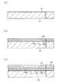
図5(a)に示すように、まず、ガラス基板30上に、プラズマCVD法を用いて二酸化珪素(SiO2)で構成された下地保護層31を形成する。その後、スパッタ法を用いて前記ガラス基板30の図中左端部を除いたほぼ全面に渡ってチタン(Ti)/銅(Cu)/窒化チタン(TiN)の薄膜を順次形成する(図5(b)参照)。本実施形態では、チタン(Ti)で構成された薄膜の膜厚が100nm、銅(Cu)で構成された薄膜の膜厚が500nm、窒化チタン(TiN)で構成された薄膜の膜厚が100nmである。そして、チタン(Ti)で構成された前記薄膜が前記第1導電層M1に対応し、銅(Cu)で構成された前記薄膜が前記第2導電層M2に対応し、窒化チタン(TiN)で構成された前記薄膜が前記第3導電層M3に対応する。そして、このように第1〜第3導電層M1,M2,M3をそれぞれスパッタ法を用いて形成することで蒸着法といった他の方法で形成する場合と比較してその成膜温度を低くすることができる。この結果、ガラス基板30や下地保護層31に加熱による欠陥等が生じるのを防止することができる。
As shown in FIG. 5A, first, a base
続いて、図5(c)に示すように、前記第3導電層M3上にCVD法等を用いて二酸化珪素(SiO2)を積層することで下地絶縁膜32を形成する。このとき、下地絶縁膜32の膜厚が2ε/3.5μm以上になるように形成する。その後、プラズマCVD法等を用いて前記アモルファスシリコン層ASを形成した後、レーザアニール法又は急速加熱法により結晶粒を成長させて多結晶シリコンを形成する。そして、図6(a)に示すように、その多結晶シリコンをフォトリソグラフィ法によりパターニングして島状のシリコン層33を形成する。続いて、シリコン層33及び下地絶縁膜32上に二酸化珪素(SiO2)で構成された膜厚約30nm〜200nmのゲート絶縁膜34を形成する。このゲート絶縁膜34の形成は、プラズマCVD法、熱酸化法等により行う。
Subsequently, as shown in FIG. 5C, a
次に、図6(b)に示すように、ゲート絶縁膜34上にイオン注入選択マスクMS1を形成し、この状態でリンイオン(P)を約1×1015cm-2のドーズ量でイオン注入する。その結果、シリコン層33中に高濃度ソース領域33HS及び高濃度ドレイン領域33HDがそれぞれ形成される。
Next, as shown in FIG. 6B, an ion implantation selection mask MS1 is formed on the
次に、前記イオン注入選択マスクMS1をアッシングして除去した後に、ゲート絶縁膜34上に膜厚約500nm程度のアルミニウム(Al)膜を形成する。
その後、前記アルミニウム(Al)膜をパターニングすることにより、図6(c)に示すゲート電極35を形成する。このゲート電極35は、前記駆動トランジスタQdのゲートに対応する。
Next, after the ion implantation selection mask MS1 is removed by ashing, an aluminum (Al) film having a thickness of about 500 nm is formed on the gate insulating film.
Then, the
続いて、前記ゲート電極35をマスクとし、前記シリコン層33に対してリンイオン(P)を約4×1013cm-2のドーズ量でイオン注入する。その結果、図7(a)に示すように、シリコン層33中に低濃度ソース領域33LS及び低濃度ドレイン領域33LDが形成される。
Subsequently, phosphorus ions (P) are ion-implanted into the
次に、ゲート絶縁膜34及びゲート電極35上の全面に渡って二酸化珪素(SiO2)で構成された第1層間絶縁膜ID1を形成する。続いて、フォトリソグラフィ法及びエッチングによって、図7(a)に示すように、駆動トランジスタQdのソース電極36に対応する位置に第1電極用コンタクトホールC1を、ドレイン電極37に対応する位置に第2電極用コンタクトホールC2を、それぞれ形成する。そして、前記第1層間絶縁膜ID1上に、銅(Cu)やアルミニウム(Al)といった導電性材料からなる導電層を成膜およびパターン形成することにより、先に形成した第1及び第2電極用コンタクトホールC1,C2に導電性材料を埋め込むとともに、高濃度ソース領域33HSに対応した位置にソース電極36を、高濃度ドレイン領域33HDに対応した位置にドレイン電極37を、それぞれ形成する。ソース電極36及びドレイン電極37はそれぞれその膜厚が約200nmないし800nm程度となるように形成する。また、ドライエッチング処理を施すことで、第1層間絶縁膜ID1、ゲート絶縁膜34、下地絶縁膜32を貫通して開孔したコンタクトホールHを形成する。つまり、このコンタクトホールHは、前記導電層MLを構成する第3導電層M3に至るように形成されている。
Next, a first interlayer insulating film ID1 made of silicon dioxide (SiO 2 ) is formed over the entire surface on the
さらに、第1層間絶縁膜ID1、ソース電極36、ドレイン電極37、導電層M(図中右端側)上、及び、コンタクトホールH内にそれぞれ二酸化珪素(SiO2)で構成された第2層間絶縁膜ID2を形成する。この第2層間絶縁膜ID2は、その膜厚が約100nm〜2μm程度となるように形成されることが望ましい。その後、第2層間絶縁膜ID2上に感光性ポリイミドを塗布、乾燥、露光、現像、焼成する平坦化絶縁膜40を形成する。
Further, a second interlayer insulating layer made of silicon dioxide (SiO 2 ) on the first interlayer insulating film ID1, the
その後、平坦化絶縁膜40をマスクとしてドライエッチングすることで、ドレイン電極37に対応する位置に前記平坦化絶縁膜40及び第1及び第2層間絶縁膜ID1,ID2をそれぞれ開孔した陽極用コンタクトホールCaを形成する。
また、スパッタ法等を用いて前記陽極用コンタクトホールCaにクロム(Cr)を埋め込む。
Thereafter, dry etching is performed using the
Further, chromium (Cr) is embedded in the anode contact hole Ca by using a sputtering method or the like.
その後、図7(b)に示すように、第1層間絶縁膜ID1及び前記陽極用コンタクトホールCaに埋め込まれたクロム(Cr)上の所定の位置にパターニングしてクロム(Cr)で構成された第1の電極層41aを形成する。この結果、第1の電極層41aは前記ドレイン電極37と陽極用コンタクトホールCaを介して電気的に接続される。また、ドライエッチング等を施すことで前記コンタクトホールH内及び前記導電層M(図中右端側)上に形成された第2層間絶縁膜ID2を削除する。
After that, as shown in FIG. 7B, the first interlayer insulating film ID1 and the chrome (Cr) embedded in the anode contact hole Ca are patterned at predetermined positions on the first interlayer insulating film ID1 and made of chrome (Cr). The
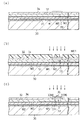
次に、図8に示すように、平坦化絶縁膜40及び第1の電極層41a上に、CVD法、スパッタ法、蒸着法等を用いてSiO2、TiO2、SiN等の無機質膜を形成する。そして、第1の電極層41aの一部が露出する態様にて形成されるように、同無機質膜に開口部をパターニングして第1バンク層42aを形成する。第1バンク層42aは、その膜厚が約50nmとなるように形成されている。
Next, as shown in FIG. 8, an inorganic film such as SiO 2 , TiO 2 , SiN or the like is formed on the
続いて、その端部を除いた前記第1バンク層42a上に第2バンク層42bが形成される。第2バンク層42bは、アクリル樹脂、ポリイミド樹脂等の通常の感光性樹脂をスピンコーターやスリットコーターなどで基板全面に塗布し、ホットプレートやオーブンなどで乾燥させた後、所定パターンのフォトマスクを通して露光し、現像液で不要部分の樹脂を除去し、200〜400℃で焼成する方法で形成される。ここでは、画素が形成される領域と、導電層MLに達するコンタクトホールHが形成される領域に開口部を形成している。第2バンク層42bはその膜厚が0.1〜3.5μmの範囲が好ましく、特に2μm程度がよい。第2バンク層42bはその厚さが0.1μm未満では、正孔注入層43及び発光層44の合計膜厚より第2バンク層42bが薄くなり、発光層44が上部開口部から溢れるおそれがあるので好ましくない。また、膜厚が3.5μmを越えると、上部開口部による段差が大きくなり、第2バンク層42b上に形成される透明導電層47が断線する恐れがある。
Subsequently, a
また、図8に示すように、前記導電層MLが外方に突出された領域が形成される。この外方に突出された部分の導電層MLが接続ポートPoになる。このようにして接続ポートPoが形成される。 Further, as shown in FIG. 8, a region is formed in which the conductive layer ML protrudes outward. The portion of the conductive layer ML protruding outward becomes the connection port Po. In this way, the connection port Po is formed.
その後、第1及び第2バンク層42a,42bの表面に、親液性を示す領域と、撥液性を示す領域を形成する。本実施例においてはプラズマ処理工程により、各領域を形成するものとしている。具体的には、前記プラズマ処理工程は、第1の電極層41a及び第1バンク層42aを親液性にする親液化工程と、第2バンク層42bを撥液性にする撥液化工程とを少なくとも具備している。
Thereafter, a region showing lyophilicity and a region showing liquid repellency are formed on the surfaces of the first and second bank layers 42a and 42b. In this embodiment, each region is formed by a plasma treatment process. Specifically, the plasma treatment step includes a lyophilic step for making the
詳しくは、第1及び第2バンク層42a,42bを形成したガラス基板30を所定温度(例えば70〜80℃程度)に加熱し、次いで親液化工程として大気圧下で酸素を反応ガスとするプラズマ処理(O2プラズマ処理)を行う。続いて、撥液化工程として大気圧下で4フッ化メタンを反応ガスとするプラズマ処理(CF4プラズマ処理)を行い、プラズマ処理のために加熱されたガラス基板30を室温まで冷却することで、第1バンク層42aの表面を親液性に、第2バンク層42bの表面を撥液性にする。
Specifically, the
その後、第1の電極層41a上に正孔注入層43及び発光層44をインクジェット法により形成する(図9(a)参照)。詳しくは、発光層44は、正孔注入層43を形成する所定の材料を含む組成物インクを吐出・乾燥した後に、発光層44を形成する所定の材料を含む組成物インクを吐出・乾燥することにより形成される。前記組成物インクは、前記撥液性及び撥液性化によって前記第1及び第2バンク層42a,42bによって構成される画素20に確実に塗布される。尚、この発光層44の形成工程以降は、正孔注入層43及び発光層44の酸化・吸湿を防止するため、窒素雰囲気又はアルゴン雰囲気といった不活性ガス雰囲気で行うことが好ましい。
Thereafter, a
続いて、図9(b)に示すように接続ポートPoを除いた発光層44、第1バンク層42a及び第2バンク層42b、及び、コンタクトホールHの全面に渡って電子注入層46を形成する。この電子注入層46は透明な材料であり、加熱蒸着法によって形成する。その後、図10(a)に示すように、電子注入層46上には透明な材料で構成された透明導電層47を、スパッタ法、真空蒸着法、CVD法などの方法によって形成する。この透明導電層47は前記した有機EL素子OLEDの陰極E2を構成する電極層である。従って、透明導電層47(有機EL素子OLEDの陰極E2)は、電子注入層48を介して前記導電層MLを構成する第3導電層M3に電気的に接続されている。
Subsequently, as shown in FIG. 9B, the
尚、この透明導電層47は、本実施形態においては、スズドープ酸化インジウム(ITO)で構成されている。
透明導電層47上には、透明な材料で構成された薄膜封止層41bを形成する。本実施形態においては、薄膜封止層41bは酸化窒化珪素(SiOxNy)からなり、スパッタ法、CVD法などの既知の適切な方法で形成される。ただし、前記接続ポートPoに薄膜封止層が形成されると導通できなくなるので、薄膜封止層41b形成時には、前記接続ポートPoをメタルマスクでカバーするなどの手段をとると良い。また、この薄膜封止層41bは、接続ポートPoを構成する図中右端側の導電層ML上にも形成されている。
The transparent
On the transparent
最後に、図10(b)に示すように、基板外周や実装端子接続部(図示せず)、前記接続ポートPoを除いたガラス基板30のほぼ全面にエポキシ樹脂などからなる透明な接着剤を塗布し、封止基板50を接合する。このようにして、表示パネル部12が製造される。
Finally, as shown in FIG. 10B, a transparent adhesive made of an epoxy resin or the like is applied to almost the entire surface of the
尚、特許請求の範囲に記載の基板、電気光学装置、接続部及び能動素子は、それぞれ、本実施形態におけるガラス基板30、有機ELディスプレイ10、コンタクトホールH及び駆動トランジスタQdに対応している。また、特許請求の範囲に記載の素子形成層は、本実施形態における第1層間絶縁膜ID1またはゲート絶縁膜34に対応している。また、特許請求の範囲に記載の絶縁層は、本実施形態における下地絶縁膜32に対応している。さらに、特許請求の範囲に記載の突出部及び透明性導電膜は、それぞれ、本実施形態における接続ポートPo及び透明導電層47に対応している。さらに、特許請求の範囲に記載のバンク層は、本実施形態における第1バンク層42aまたは第2バンク層42bに対応している。また、特許請求の範囲に記載の金属層は本実施形態における第2導電層M2に対応している。
The substrate, the electro-optical device, the connection unit, and the active element described in the claims correspond to the
前記実施形態によれば、以下のような特徴を得ることができる。
(1)前記実施形態では、各画素20に形成される有機EL素子OLEDの陰極E2を全てコンタクトホールHを介して導電層MLに電気的に接続されるようにした。この結果、表示パネル部12上に形成される位置によって有機EL素子OLEDの陰極E2の電位に差が生じることはない。つまり、例えば、全ての画素20に同じ電圧レベルのデータ信号D1,D2,…,Dmを供給したとき、画素20が形成される位置によって有機EL素子OLEDの輝度に差が生じることはないので、その分、表示ムラを低減させることができる。
According to the embodiment, the following features can be obtained.
(1) In the above embodiment, all the cathodes E2 of the organic EL elements OLED formed in each
従って、たとえば、陰極E2をスズドープ酸化インジウム(ITO)といった比較的導電率が低い(抵抗率が比較的高い)透明材料で構成されたトップエミッションタイプの有機ELディスプレイであっても、データ信号D1,D2,…,Dmに応じた画像を精度良く表示させることができる。 Therefore, even if the cathode E2 is a top emission type organic EL display composed of a transparent material such as tin-doped indium oxide (ITO) having a relatively low conductivity (relatively high resistivity), the data signal D1, Images corresponding to D2,..., Dm can be displayed with high accuracy.
(2)前記実施形態では、前記導電層MLはその一端が表示パネル部12から直接外方に突出されている。そして、その突出された導電層MLを接続ポートPoとして使用するようにした。従って、前記接続ポートPoに各種外部装置を接続することで特別なインターフェースといった接続手段を設けることなく有機EL素子OLEDの各陰極E2の電位を直接制御することができる。
(2) In the embodiment, one end of the conductive layer ML projects directly outward from the
(3)前記実施形態では、チタン(Ti)で第1導電層M1を構成した。従って、第1導電層M1を下地保護層31に密着良く形成することができる。また、銅(Cu)で第2導電層M2を構成した。従って、導電層MLの導電率を高くすることができるので、その分、陰極E2が表示パネル部12上に形成される位置によって、電位差が生じることを抑制することができる。
(3) In the said embodiment, the 1st conductive layer M1 was comprised with titanium (Ti). Therefore, the first conductive layer M1 can be formed with good adhesion to the base
さらに、窒化チタン(TiN)で第3導電層M3を構成した。第2導電層M2を構成する銅(Cu)と下地絶縁膜32を構成する(SiO2)とが反応して、その結果、第2導電層M2の導電率が低下する若しくは下地絶縁膜32の絶縁性が低下するのを防止することができる。
Further, the third conductive layer M3 was made of titanium nitride (TiN). Copper (Cu) constituting the second conductive layer M2 reacts with (SiO 2 ) constituting the
(4)前記実施形態では、ガラス基板30上に下地保護層31、導電層ML、下地絶縁膜32、ゲート絶縁膜34、第1及び第2層間絶縁膜ID1,ID2、平坦化絶縁膜40を形成した。そして、平坦化絶縁膜40を形成した後、第1及び第2バンク層42a,42bを形成し、ドライエッチング処理を施すことで、先に形成された下地絶縁膜32、ゲート絶縁膜34、第1及び第2層間絶縁膜ID1,ID2、第1バンク層42aの各々を除去してコンタクトホールHを形成した。その後、このコンタクトホールH上に順次、電子注入層46、透明導電層47を形成した。
(4) In the embodiment, the base
このようにすることで、透明導電層47と導電層MLとを電気的に接続することができる。この結果、表示ムラを低減させた有機ELディスプレイ10を製造することができる。
By doing in this way, the transparent
(5)前記実施形態では、第1〜第3導電層M1,M2,M3をそれぞれスパッタ法を用いて形成した。従って、蒸着法といった他の方法で形成する場合と比較してその成膜温度を低くすることができる。この結果、ガラス基板30や下地保護層31に欠陥等が生じるのを防止することができる。
(5) In the said embodiment, the 1st-3rd conductive layers M1, M2, M3 were each formed using the sputtering method. Therefore, the film formation temperature can be lowered as compared with the case of forming by other methods such as vapor deposition. As a result, it is possible to prevent the
(6)前記実施形態では、下地絶縁膜32を、その膜厚が2ε/3.5μm以上になるように形成した。従って、下地絶縁膜32上に形成されるシリコン層33、データ線X1,X2,…,Xm及び走査線Y1,Y2,…,Yn等に導電層MLを構成する材料が拡散するのを確実に防止することができる。また、導電層MLと、シリコン層33、データ線X1、X2、…、Xm及び走査線Y1,Y2,…,Ynの間に生じる寄生容量を低減し、駆動回路を安定して動作させ、表示品質を向上させることができる。
(第2実施形態)
次に、本発明を具体化した第2実施形態を図11〜図13に従って説明する。
まず、本発明の第2実施形態に係る表示パネル部の構造について図11に従って説明する。尚、図11は、第1の実施形態の図3中のA−A線に沿う断面に対応している。
(6) In the above embodiment, the
(Second Embodiment)
Next, a second embodiment of the present invention will be described with reference to FIGS.
First, the structure of the display panel unit according to the second embodiment of the present invention will be described with reference to FIG. FIG. 11 corresponds to a cross section taken along the line AA in FIG. 3 of the first embodiment.
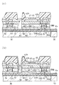
本実施形態に係る表示パネル部12aは、そのコンタクトホールHrと第3導電層M3との電気的接続するための構造及びその製造方法が異なっていること以外は前記第1実施形態と同じである。従って、コンタクトホールHrと第3導電層M3とを電気的に接続するための構造及びその製造方法以外は、その詳細な説明は省略する。
The
図11に示すように、表示パネル部12aは、その下地絶縁膜32及びゲート絶縁膜34を連通して開孔した第3のコンタクトホールC3が形成されている。
また、この第3のコンタクトホールC3には、駆動トランジスタQdを構成するゲート電極35を構成する導電性材料と同じ材料が埋め込まれている。また、この第3のコンタクトホールC3に埋め込まれた導電性材料はゲート絶縁膜34上の一部に乗り上げて形成されている。そして、このゲート絶縁膜34上の一部に乗り上げて形成された導電性材料は第1コンタクト部CON1になる。そして、第1コンタクト部CON1に対応する位置に、前記ゲート絶縁膜34上に形成された第1層間絶縁膜ID1を開孔する第4のコンタクトホールC4が形成されている。
As shown in FIG. 11, the
The third contact hole C3 is filled with the same material as the conductive material that forms the
前記第4のコンタクトホールC4には、駆動トランジスタQdを構成するソース電極36またはドレイン電極37を構成する導電性材料と同じ材料が埋め込まれている。また、この第4のコンタクトホールC4に埋め込まれた導電性材料は第1層間絶縁膜ID1上の一部に乗り上げて形成されている。そして、この第1層間絶縁膜ID1上の一部に乗り上げて形成された導電性材料は第2コンタクト部CON2になる。そして、第2コンタクト部CON2に対応する位置に、第1及び第2バンク層42a,42b、平坦化絶縁膜40及び第2層間絶縁膜ID2をそれぞれ貫通して形成されるコンタクトホールHrが設けられている。そして、このコンタクトホールHrには、上記第1実施形態に記載されたように、電子注入層46、透明導電層47及び薄膜封止層41bが順次形成されている。従って、透明導電層47は前記第2コンタクト部CON2及び第1コンタクト部CON1を介して前記導電層MLと電気的に接続された状態になる。この結果、前記第1実施形態と同様な効果を得ることができる。
In the fourth contact hole C4, the same material as the conductive material constituting the
次に、本実施形態の有機ELディスプレイ10の製造方法を図12〜図14に従って説明する。尚、コンタクトホールHと導電層MLとの電気的接続をする部分の製造方法についてのみ説明し、他の前記第1実施形態と同じ構造については符号を付しその製造方法の詳細は省略する。
Next, the manufacturing method of the
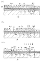
まず、ガラス基板30上に下地保護層31、第1、第2及び第3導電層M1,M2,M3、下地絶縁膜32、シリコン層33及びゲート絶縁膜34を順次形成した後、図12(a)に示すように、前記シリコン層33と隣接して形成されるシリコン層33a(図中左側に形成されたシリコン層)との間に開孔部Qr1を備えたマスクMr1を設ける。続いて、ドライエッチング処理を施すことによって図12(b)に示すように、開孔部Qr1に対応する前記ゲート絶縁膜34及び下地絶縁膜32を除去して第3のコンタクトホールC3を形成する。同時に、後述する接続ポートPoに対向する位置(図中右側端)の前記ゲート絶縁膜34及び下地絶縁膜32も除去しておく。
First, a base
その後、シリコン層33のチャネル領域33C及び第3のコンタクトホールC3に対応した領域に開孔部Qr2,Qr3を備えたマスクMr2を設ける。続いて、スパッタ法等を用いてアルミニウム(Al)膜を形成する。その後、前記マスクMr2を除去することで、アルミニウム(Al)で構成された膜厚約500nm程度のゲート電極35及び第1コンタクト部CON1がそれぞれ形成される(図12(c)参照)。従って、第1コンタクト部CON1はゲート電極35と同時に形成される。続いて、前記ゲート電極35をマスクとし、前記シリコン層33に対してリンイオン(P)を約4×1013cm-2のドーズ量でイオン注入してシリコン層33中に低濃度ソース領域33LS及び低濃度ドレイン領域33LDを形成する。
Thereafter, a mask Mr2 having openings Qr2 and Qr3 is provided in a region corresponding to the
次に、ゲート絶縁膜34、ゲート電極35及び第1コンタクト部CON1上に第1層間絶縁膜ID1を形成し(図13(a)参照)、その形成した第1層間絶縁膜ID1をCMP(化学的機械的研磨)等を用いて平坦化処理する。その後、図13(b)に示すように、前記第1層間絶縁膜ID1上に第1コンタクト部CON1に対向する位置に開孔部Qr4が、また、シリコン層33に形成された高濃度ソース領域33HS及び高濃度ドレイン領域33HDに対向する位置に開孔部Qr5a,Qr5bがそれぞれ形成されたマスクMr3を設ける。そして、エッチング処理を施すことによって、図13(c)に示すように、第1コンタクト部CON1に対応する位置に第4のコンタクトホールC4が形成される。また、駆動トランジスタQdのソース電極36に対応する位置に第1電極用コンタクトホールC1が、ドレイン電極37に対応する位置に第2電極用コンタクトホールC2が、それぞれ形成される。また同時に、後述する接続ポートPoに対応する位置の第1層間絶縁膜ID1も除去しておく。
Next, a first interlayer insulating film ID1 is formed on the
そして、前記第1層間絶縁膜ID1上に、銅(Cu)やアルミニウム(Al)といった導電性材料からなる導電層を形成することにより、先に形成した第4のコンタクトホールC4、第1及び第2電極用コンタクトホールC1,C2に導電性材料を埋め込む。その結果、第1コンタクト部CON1と電気的に接続し第1層間絶縁膜ID1上の一部に乗り上げた位置に形成される第2コンタクト部CON2が形成される。また、高濃度ソース領域33HSに対応した位置にソース電極36が、高濃度ドレイン領域33HDに対応した位置にドレイン電極37が、それぞれ形成される。従って、第2コンタクト部CON2はソース電極36及びドレイン電極37と同時に形成される。
Then, a conductive layer made of a conductive material such as copper (Cu) or aluminum (Al) is formed on the first interlayer insulating film ID1, thereby forming the fourth contact hole C4, the first and first layers formed previously. A conductive material is embedded in the two-electrode contact holes C1 and C2. As a result, a second contact portion CON2 is formed which is electrically connected to the first contact portion CON1 and formed at a position over a part of the first interlayer insulating film ID1. A
続いて、図14(a)に示すように、第1層間絶縁膜ID1、第2コンタクト部CON2、ソース電極36及びドレイン電極37上に二酸化珪素(SiO2)からなる第2層間絶縁膜ID2を形成する。その後、第2層間絶縁膜ID2上に二酸化珪素(SiO2)で構成された平坦化絶縁膜40を形成する。形成された平坦化絶縁膜40をCMP(化学的機械的研磨)等を用いて平坦化処理する。その後、第2層間絶縁膜ID2および平坦化絶縁膜40のドレイン電極37に対向する位置にコンタクトホールを形成する。同時に第2コンタクト部CON2に対向する位置にもコンタクトホールを形成する。また同時に、後述する接続ポートPoに対向する位置の第2層間絶縁膜ID2および平坦化絶縁膜40も除去しておく。
Subsequently, as shown in FIG. 14A, a second interlayer insulating film ID2 made of silicon dioxide (SiO 2 ) is formed on the first interlayer insulating film ID1, the second contact portion CON2, the
その後、図14(b)に示すように、平坦化絶縁膜40上に第1の電極層41a、第1バンク層42a及び第2バンク層42bを順次形成する。第1バンク層42a成膜後に発光領域に開口部を形成するが、それと同時にドレイン電極37に対応する位置にもコンタクトホールを形成する。第2バンク層42bは、感光性のアクリル樹脂やポリイミド樹脂を塗布・乾燥後、露光・現像・焼成することで画素の開口部を形成するが、それと同時に、ドレイン電極37に対応する位置にも開口部を形成する。また、それぞれの開口部を形成するのと同時に、後述する接続ポートPoに対応する位置の第1バンク層42a及び第2バンク層42bも除去しておく。
Thereafter, as shown in FIG. 14B, a
この状態で、図14(b)に示すような開口部Qoに対応した位置が開孔したコンタクトホールHrが形成される。
また、ガラス基板30の端部(図中右端側)に示すような前記導電層MLが外方に突出された領域が形成される。この外方に突出された部分の導電層MLが接続ポートPoになる。このようにして接続ポートPoが形成される。
In this state, a contact hole Hr having a position corresponding to the opening Qo as shown in FIG. 14B is formed.
In addition, a region is formed in which the conductive layer ML protrudes outward as shown at the end portion (right end side in the drawing) of the
そして、プラズマ処理によって第1及び第2バンク層42a、42b表面に親液性と撥液性の領域を形成し、第1の電極層41a上に正孔注入層43及び発光層44をインクジェット法により形成する。
Then, lyophilic and lyophobic regions are formed on the surfaces of the first and second bank layers 42a and 42b by plasma treatment, and the
その後、発光層44、第1バンク層42a及び第2バンク層42b、及び、コンタクトホールHの全面に渡って電子注入層46が形成されている。この電子注入層46は透明な材料で形成されている。電子注入層46上には透明な材料で構成された透明導電層47が形成されている。透明導電層47は前記した有機EL素子OLEDの陰極E2を構成する電極層である。従って、透明導電層47(有機EL素子OLEDの陰極E2)は、電子注入層46を介して前記導電層MLを構成する第3導電層M3に電気的に接続されている。
Thereafter, the
透明導電層47上には、透明な材料で構成された薄膜封止層41bを形成する。本実施形態においては、薄膜封止層41bは酸化窒化珪素(SiOxNy)からなり、スパッタ法、CVD法などの既知の適切な方法で形成される。ただし、前記接続ポートPoに薄膜封止層が形成されると導通できなくなるので、薄膜封止層41b形成時には、前記接続ポートPoをメタルマスクでカバーするなどの手段をとると良い。
On the transparent
最後に、基板外周や実装端子接続部(図示せず)、前記接続ポートPoを除いたガラス基板30のほぼ全面にエポキシ樹脂などからなる透明な接着剤を塗布し、封止基板50を接合することで図11に示す表示パネル部12が製造される。
Finally, a transparent adhesive made of epoxy resin or the like is applied to almost the entire surface of the
このように有機ELディスプレイ10を製造することで、コンタクトホールHは前記導電層MLに至るまで形成される必要はなく、前記したように、第1層間絶縁膜ID1上に渡って先に形成された前記第2コンタクト部CON2に至るまで形成すればよい。この結果、第1実施形態の有機ELディスプレイに比べてコンタクトホールHを容易に形成することができる。この結果、第1実施形態の有機ELディスプレイに比べてその歩留まりを向上させることができる。
By manufacturing the
前記実施形態によれば、以下のような特徴を得ることができる。
(1)前記実施形態では、ゲート絶縁膜34上に導電層MLに電気的に接続された第1コンタクト部CON1を形成した。そして、第1コンタクト部CON1はゲート電極35と同時に形成した。第1層間絶縁膜ID1上に第1コンタクト部CON1に電気的に接続された第2コンタクト部CON2を形成した。そして、第2コンタクト部CON2はソース電極36及びドレイン電極37と同時に形成した。そして、第1層間絶縁膜ID1上に第2層間絶縁膜ID2、平坦化絶縁膜40、第1及び第2バンク層42a,42bの各層を形成して開口部(コンタクトホールなど)を形成するのと同時に、コンタクトホールHrに対応する部分にも開口部を形成することによって、前記第2コンタクト部CON2に至るコンタクトホールHrを形成した。その後、このコンタクトホールHr上に順次、電子注入層46、透明導電層47及び薄膜封止層41bを形成した。
According to the embodiment, the following features can be obtained.
(1) In the above embodiment, the first contact part CON1 electrically connected to the conductive layer ML is formed on the
従って、導電層MLまでドライエッチング処理を施すことなく透明導電層47と導電層MLとを電気的に接続することができる。この結果、コンタクトホールHを容易に形成することができるので、その歩留まりを向上させることができる。
(第3実施形態)
次に、第1又は第2実施形態で説明した電気光学装置としての有機ELディスプレイ10の電子機器の適用について図15に従って説明する。有機ELディスプレイ10は、モバイル型のパーソナルコンピュータ、携帯電話、デジタルカメラ等種々の電子機器に適用できる。
Therefore, the transparent
(Third embodiment)
Next, application of the electronic apparatus of the
図15は、モバイル型パーソナルコンピュータの構成を示す斜視図を示す。図15において、パーソナルコンピュータ70は、キーボード71を備えた本体部72と、前記有機ELディスプレイ10を用いた表示ユニット73とを備えている。この場合においても、有機ELディスプレイ10を用いた表示ユニット73は前記第1及び第2実施形態と同様な効果を発揮する。
FIG. 15 is a perspective view showing the configuration of a mobile personal computer. In FIG. 15, the
尚、発明の実施形態は、上記実施形態に限定されるものではなく、以下のように実施してもよい。
○上記各実施形態では、第1導電層M1と第2導電層M2と第3導電層M3とで1つの導電層MLを構成した。これを、導電層MLを一つの材料で構成された単一の層で構成するようにしてもよい。この場合、導電層MLは、チタン(Ti)、タンタル(Ta)、タングステン(W)、モリブデン(Mo)、バナジウム(V)、ジルコニウム(Zr)、及びこれらの合金またはシリサイドで構成されることが好ましい。
In addition, embodiment of invention is not limited to the said embodiment, You may implement as follows.
In the above embodiments, the first conductive layer M1, the second conductive layer M2, and the third conductive layer M3 constitute one conductive layer ML. Alternatively, the conductive layer ML may be composed of a single layer composed of one material. In this case, the conductive layer ML may be composed of titanium (Ti), tantalum (Ta), tungsten (W), molybdenum (Mo), vanadium (V), zirconium (Zr), and alloys or silicides thereof. preferable.
○上記各実施形態では、第1導電層M1と第2導電層M2と第3導電層M3とで1つの導電層MLを構成した。これを、導電層MLを第1導電層M1と第2導電層M2のみから成る2層で構成するようにしてもよい。この場合、第1導電層M1は、チタン(Ti)、タンタル(Ta)、タングステン(W)、モリブデン(Mo)、及びこれらの合金またはシリサイドで構成されることが好ましい。また、第2導電層M2は、アルミニウム(A1)、ニッケル(Ni)及び白金(Pt)で構成されることが好ましい。 In the above embodiments, the first conductive layer M1, the second conductive layer M2, and the third conductive layer M3 constitute one conductive layer ML. Alternatively, the conductive layer ML may be composed of two layers including only the first conductive layer M1 and the second conductive layer M2. In this case, the first conductive layer M1 is preferably composed of titanium (Ti), tantalum (Ta), tungsten (W), molybdenum (Mo), and alloys or silicides thereof. The second conductive layer M2 is preferably composed of aluminum (A1), nickel (Ni), and platinum (Pt).
○上記各実施形態では、第1導電層M1をチタン(Ti)で構成した。また、第2導電層M2を銅(Cu)で構成した。さらに、第3導電層M3を窒化チタン(TiN)で構成した。 In each of the above embodiments, the first conductive layer M1 is made of titanium (Ti). The second conductive layer M2 was made of copper (Cu). Furthermore, the third conductive layer M3 was composed of titanium nitride (TiN).
これを、タンタル(Ta)、タングステン(W)、モリブデン(Mo)、及びこれらの合金またはシリサイドで第1導電層M1を構成してもよい。また、アルミニウム(A1)、ニッケル(Ni)、白金(Pt)、金(Au)、銀(Ag)、及びこれらの合金またはシリサイドで第2導電層M2を構成してもよい。さらに、チタン(Ti)、タンタル(Ta)、タングステン(W)、モリブデン(Mo)、及びこれらの合金またはシリサイドで第3導電層M3を構成してもよい。
このようにすることで上記実施形態と同じ効果を奏することができる。
The first conductive layer M1 may be formed of tantalum (Ta), tungsten (W), molybdenum (Mo), and an alloy or silicide thereof. The second conductive layer M2 may be made of aluminum (A1), nickel (Ni), platinum (Pt), gold (Au), silver (Ag), and alloys or silicides thereof. Further, the third conductive layer M3 may be composed of titanium (Ti), tantalum (Ta), tungsten (W), molybdenum (Mo), and alloys or silicides thereof.
By doing in this way, the same effect as the above-mentioned embodiment can be produced.
○上記各実施形態では、電気光学装置として、その発光層が有機EL素子で構成された有機ELディスプレイ10に具体化したが、これに限定されるものではなく、トップエミッションタイプの電気光学装置ならどのような電気光学装置に適応してもよい。
In each of the above embodiments, the electro-optical device is embodied as the
○上記各実施形態では、各画素20に形成される有機EL素子OLEDの陰極E2を全てコンタクトホールH,Hrを介して導電層MLに電気的に接続されるようにした。これをコンタクトホールH,Hrではなく、他の形状を成したもので有機EL素子OLEDの陰極E2と導電層MLとを電気的に接続するようにしてもよい。
In each of the above embodiments, the cathode E2 of the organic EL element OLED formed in each
○上記各実施形態では、有機EL素子OLEDの陰極E2をスズドープ酸化インジウム(ITO)で構成された陰極を使用したが、これに限定されるものではなく、例えば、陰極E2が酸化亜鉛(ZnO)といった透明導電性薄膜で構成された有機ELディスプレイに適応してもよい。つまり、有機EL素子OLEDの陰極E2を構成する材料には限定されるものではない。 In each of the above embodiments, the cathode composed of tin-doped indium oxide (ITO) is used as the cathode E2 of the organic EL element OLED. However, the present invention is not limited to this. You may apply to the organic electroluminescent display comprised with such a transparent conductive thin film. That is, the material constituting the cathode E2 of the organic EL element OLED is not limited.
○上記各実施形態では、各層の成膜方法は上記実施形態に記載された方法に限定されるものではなく、他の方法を用いて形成されるようにしてもよい。
○上記各実施形態では、ポリシリコンで構成されたシリコン層33をチャネル領域33Cとした駆動トランジスタQdで画素20を構成した有機ELディスプレイ10に対して適応した。これを、単結晶で構成されたシリコン層をチャネル領域とした駆動トランジスタで画素20を構成した有機ELディスプレイに対して適応してもよい。
In each of the above embodiments, the method for forming each layer is not limited to the method described in the above embodiment, and may be formed using other methods.
In each of the above embodiments, the present invention is applied to the
30…基板としてのガラス基板、E1…陽極、E2…陰極、発光性材料としての発光層、20…画素、10…電気光学装置としての有機ELディスプレイ、ML…導電層、H,Hr…接続部としてのコンタクトホール、Qd…能動素子としての駆動トランジスタ、ID1,34…素子形成層としての第1層間絶縁膜及びゲート絶縁膜、31…下地保護層、32…絶縁層としての下地絶縁膜、ML…導電層、M1…第1導電層、M2…金属層としての第2導電層、M3…第3導電層、Po…突出部としての接続ポート、42a,42b…バンク層として第1及び第2バンク層、41b…透明性導電膜としての薄膜封止層、70…電子機器としてのモバイル型のパーソナルコンピュータ。
DESCRIPTION OF
Claims (14)
前記基板と前記陽極との間に形成された導電層と、
前記陰極と前記導電層とを電気的に接続するための接続部とを備えていることを特徴とする電気光学装置。 On a substrate, an anode, a cathode formed at a position facing the anode, and a luminescent material provided between the anode and the cathode, the anode being a pixel provided with the luminescent material In the electro-optical device formed for each,
A conductive layer formed between the substrate and the anode;
An electro-optical device comprising: a connecting portion for electrically connecting the cathode and the conductive layer.
前記接続部は前記画素毎に備えられていることを特徴とする電気光学装置。 The electro-optical device according to claim 1.
The electro-optical device, wherein the connection portion is provided for each pixel.
前記接続部はコンタクトホールで構成されていることを特徴とする電気光学装置。 The electro-optical device according to claim 1,
The electro-optical device is characterized in that the connecting portion is formed of a contact hole.
前記基板上には前記発光性材料に供給される電流を制御するための能動素子が形成される素子形成層を備え、
前記素子形成層と前記導電層との間には前記素子形成層と前記導電層とを電気的に切断するための絶縁層が形成されていることを特徴とする電気光学装置。 The electro-optical device according to any one of claims 1 to 3,
An element forming layer on which an active element for controlling a current supplied to the light emitting material is formed on the substrate;
An electro-optical device, wherein an insulating layer for electrically cutting the element forming layer and the conductive layer is formed between the element forming layer and the conductive layer.
前記絶縁層は、その誘電率をεとしたとき、膜厚が2ε/3.5μm以上であることを特徴とする電気光学装置。 The electro-optical device according to claim 4.
2. The electro-optical device according to claim 1, wherein the insulating layer has a film thickness of 2ε / 3.5 μm or more when the dielectric constant is ε.
前記導電層はチタン(Ti)、タンタル(Ta)、タングステン(W)、モリブデン(Mo)、バナジウム(V)、ジルコニウム(Zr)、及びこれらの合金またはシリサイドのうちの一つで構成されることを特徴とする電気光学装置。 The electro-optical device according to claim 1,
The conductive layer is composed of one of titanium (Ti), tantalum (Ta), tungsten (W), molybdenum (Mo), vanadium (V), zirconium (Zr), and alloys or silicides thereof. An electro-optical device.
前記導電層は少なくとも一層の金属層を含む複数の導電層から構成されていることを特徴とする電気光学装置。 The electro-optical device according to claim 1,
The electro-optical device, wherein the conductive layer includes a plurality of conductive layers including at least one metal layer.
前記基板上に該基板を保護する下地保護層を備え、その下地保護層は二酸化珪素で構成され、
前記複数の導電層は前記下地保護層上から順に第1導電層、第2導電層から構成される導電層であって、
前記第1導電層はチタン(Ti)、タンタル(Ta)、タングステン(W)、モリブデン(Mo)、及びこれらの合金またはシリサイドのいずれか一つで構成され、
前記第2導電層はアルミニウム(A1)、ニッケル(Ni)及び白金(Pt)、及びこれらの合金またはシリサイドのいずれか一つで構成されていることを特徴とする電気光学装置。 The electro-optical device according to claim 7.
Provided with a base protective layer for protecting the substrate on the substrate, the base protective layer is composed of silicon dioxide,
The plurality of conductive layers are conductive layers composed of a first conductive layer and a second conductive layer in order from the base protective layer,
The first conductive layer is made of any one of titanium (Ti), tantalum (Ta), tungsten (W), molybdenum (Mo), and alloys or silicides thereof.
The electro-optical device, wherein the second conductive layer is made of any one of aluminum (A1), nickel (Ni), platinum (Pt), and an alloy or silicide thereof.
前記基板上に該基板を保護する下地保護層を備え、その保護層は二酸化珪素で構成され、
前記複数の導電層は前記下地保護層上から順に第1導電層、第2導電層、第3導電層から構成され、
前記第1導電層はチタン(Ti)、タンタル(Ta)、タングステン(W)、モリブデン(Mo)、及びこれらの合金またはシリサイドのいずれか一つで構成され、
前記第2導電層は銅(Cu)、アルミニウム(A1)、ニッケル(Ni)及び白金(Pt)、及びこれらの合金またはシリサイドのいずれか一つで構成され、
前記第3導電層は窒化チタン(TiN)、チタン(Ti)、タンタル(Ta)、タングステン(W)、モリブデン(Mo)、及びこれらの合金またはシリサイドのいずれか一つで構成されていることを特徴とする電気光学装置。 The electro-optical device according to claim 7.
Provided with a base protective layer for protecting the substrate on the substrate, the protective layer is composed of silicon dioxide,
The plurality of conductive layers are composed of a first conductive layer, a second conductive layer, and a third conductive layer in order from the top protective layer,
The first conductive layer is made of any one of titanium (Ti), tantalum (Ta), tungsten (W), molybdenum (Mo), and alloys or silicides thereof.
The second conductive layer is composed of any one of copper (Cu), aluminum (A1), nickel (Ni), platinum (Pt), and alloys or silicides thereof.
The third conductive layer is composed of any one of titanium nitride (TiN), titanium (Ti), tantalum (Ta), tungsten (W), molybdenum (Mo), and alloys or silicides thereof. Electro-optical device characterized.
前記導電層は前記基板から突出して形成された突出部を備えていることを特徴とする電気光学装置。 The electro-optical device according to claim 1,
The electro-optical device, wherein the conductive layer includes a protruding portion that protrudes from the substrate.
前記基板の上方に前記導電層を形成する工程と、
前記導電層の上方に前記絶縁層、前記素子形成層、前記陽極及びバンク層を形成する工程と、
前記絶縁層に開口パターンを形成するのと同時に前記陰極と前記導電層とを電気的に接続するための接続部開口パターンを形成する工程と、
前記発光性材料を形成する工程と、
前記接続部を含む前記発光性材料を形成した領域の全面に透明性導電膜を形成する工程とを備えたことを特徴とする電気光学装置の製造方法。 An anode, a cathode formed at a position facing the anode, and a luminescent material provided between the anode and the cathode are provided on the substrate, and the luminescent material is divided into pixels. A bank layer, a conductive layer formed between the substrate and the anode, a connection part for electrically connecting the cathode and the conductive layer, and the luminescent material on the substrate In order to electrically disconnect the element forming layer and the conductive layer between the element forming layer and the conductive layer, and an element forming layer in which an active element for controlling the current supplied to the element is formed In an electro-optical device manufacturing method including the insulating layer,
Forming the conductive layer above the substrate;
Forming the insulating layer, the element forming layer, the anode and the bank layer above the conductive layer;
Forming a connection portion opening pattern for electrically connecting the cathode and the conductive layer simultaneously with forming an opening pattern in the insulating layer;
Forming the luminescent material;
And a step of forming a transparent conductive film on the entire surface of the region where the light emitting material including the connecting portion is formed.
前記導電層は第1導電層、第2導電層及び第3導電層から構成される導電層を備え
前記素子形成層は前記能動素子に信号を供給するための第1の信号線と第2の信号線とを備え、
前記第1導電層は前記第1の信号線を形成すると同時に形成され、
前記第2導電層は前記第2の信号線を形成すると同時に形成されるようにしたことを特徴とする電気光学装置の製造方法。 The method of manufacturing an electro-optical device according to claim 11.
The conductive layer includes a conductive layer including a first conductive layer, a second conductive layer, and a third conductive layer. The element formation layer includes a first signal line and a second signal line for supplying a signal to the active element. With signal lines,
The first conductive layer is formed simultaneously with forming the first signal line;
The method of manufacturing an electro-optical device, wherein the second conductive layer is formed simultaneously with the formation of the second signal line.
前記導電層はスパッタ法で形成するようにしたことを備えたことを特徴とする電気光学装置の製造方法。 The method of manufacturing an electro-optical device according to claim 11 or 12,
An electro-optical device manufacturing method, wherein the conductive layer is formed by sputtering.
Priority Applications (1)
| Application Number | Priority Date | Filing Date | Title |
|---|---|---|---|
| JP2009027076A JP2009105068A (en) | 2009-02-09 | 2009-02-09 | Electro-optical device, method for manufacturing electro-optical device and electronic equipment |
Applications Claiming Priority (1)
| Application Number | Priority Date | Filing Date | Title |
|---|---|---|---|
| JP2009027076A JP2009105068A (en) | 2009-02-09 | 2009-02-09 | Electro-optical device, method for manufacturing electro-optical device and electronic equipment |
Related Parent Applications (1)
| Application Number | Title | Priority Date | Filing Date |
|---|---|---|---|
| JP2003198128A Division JP4380242B2 (en) | 2003-07-16 | 2003-07-16 | Electro-optical device, method of manufacturing electro-optical device, and electronic apparatus |
Publications (2)
| Publication Number | Publication Date |
|---|---|
| JP2009105068A true JP2009105068A (en) | 2009-05-14 |
| JP2009105068A5 JP2009105068A5 (en) | 2009-08-06 |
Family
ID=40706501
Family Applications (1)
| Application Number | Title | Priority Date | Filing Date |
|---|---|---|---|
| JP2009027076A Withdrawn JP2009105068A (en) | 2009-02-09 | 2009-02-09 | Electro-optical device, method for manufacturing electro-optical device and electronic equipment |
Country Status (1)
| Country | Link |
|---|---|
| JP (1) | JP2009105068A (en) |
Cited By (8)
| Publication number | Priority date | Publication date | Assignee | Title |
|---|---|---|---|---|
| JP2011081916A (en) * | 2009-10-02 | 2011-04-21 | Canon Inc | Display device |
| JP2011191730A (en) * | 2009-09-08 | 2011-09-29 | Ricoh Co Ltd | Display device, manufacturing method thereof, and electronic equipment |
| JP2012129197A (en) * | 2010-12-14 | 2012-07-05 | Samsung Mobile Display Co Ltd | Organic light-emitting display device, and method of manufacturing the same |
| JP2012227138A (en) * | 2011-04-08 | 2012-11-15 | Semiconductor Energy Lab Co Ltd | Light-emitting device and manufacturing method for the same |
| JP2015154072A (en) * | 2014-02-17 | 2015-08-24 | エバーディスプレイ オプトロニクス(シャンハイ) リミテッド | Thin film transistor array substrate and manufacturing method therefor |
| JP2018109758A (en) * | 2016-12-29 | 2018-07-12 | エルジー ディスプレイ カンパニー リミテッド | Display device including auxiliary electrode |
| JP2019153569A (en) * | 2018-03-01 | 2019-09-12 | Tianma Japan株式会社 | Display device |
| WO2021176894A1 (en) * | 2020-03-03 | 2021-09-10 | ソニーグループ株式会社 | Display device, method for manufacturing display device, and electronic apparatus |
Citations (3)
| Publication number | Priority date | Publication date | Assignee | Title |
|---|---|---|---|---|
| JP2002164181A (en) * | 2000-09-18 | 2002-06-07 | Semiconductor Energy Lab Co Ltd | Display device and its manufacturing method |
| JP2003187970A (en) * | 2001-12-18 | 2003-07-04 | Seiko Epson Corp | Manufacturing method of display device and electronic equipment, display device and electronic equipment |
| JP2003295792A (en) * | 2002-01-29 | 2003-10-15 | Internatl Business Mach Corp <Ibm> | Organic led device and its manufacturing method |
-
2009
- 2009-02-09 JP JP2009027076A patent/JP2009105068A/en not_active Withdrawn
Patent Citations (3)
| Publication number | Priority date | Publication date | Assignee | Title |
|---|---|---|---|---|
| JP2002164181A (en) * | 2000-09-18 | 2002-06-07 | Semiconductor Energy Lab Co Ltd | Display device and its manufacturing method |
| JP2003187970A (en) * | 2001-12-18 | 2003-07-04 | Seiko Epson Corp | Manufacturing method of display device and electronic equipment, display device and electronic equipment |
| JP2003295792A (en) * | 2002-01-29 | 2003-10-15 | Internatl Business Mach Corp <Ibm> | Organic led device and its manufacturing method |
Cited By (11)
| Publication number | Priority date | Publication date | Assignee | Title |
|---|---|---|---|---|
| JP2011191730A (en) * | 2009-09-08 | 2011-09-29 | Ricoh Co Ltd | Display device, manufacturing method thereof, and electronic equipment |
| JP2011081916A (en) * | 2009-10-02 | 2011-04-21 | Canon Inc | Display device |
| JP2012129197A (en) * | 2010-12-14 | 2012-07-05 | Samsung Mobile Display Co Ltd | Organic light-emitting display device, and method of manufacturing the same |
| KR101889918B1 (en) | 2010-12-14 | 2018-09-21 | 삼성디스플레이 주식회사 | Organinc light emitting display device and manufacturing method for the same |
| JP2012227138A (en) * | 2011-04-08 | 2012-11-15 | Semiconductor Energy Lab Co Ltd | Light-emitting device and manufacturing method for the same |
| JP2015154072A (en) * | 2014-02-17 | 2015-08-24 | エバーディスプレイ オプトロニクス(シャンハイ) リミテッド | Thin film transistor array substrate and manufacturing method therefor |
| JP2018109758A (en) * | 2016-12-29 | 2018-07-12 | エルジー ディスプレイ カンパニー リミテッド | Display device including auxiliary electrode |
| US10388905B2 (en) | 2016-12-29 | 2019-08-20 | Lg Display Co., Ltd. | Display device having an auxiliary electrode |
| JP2019153569A (en) * | 2018-03-01 | 2019-09-12 | Tianma Japan株式会社 | Display device |
| JP7179517B2 (en) | 2018-03-01 | 2022-11-29 | Tianma Japan株式会社 | Display device |
| WO2021176894A1 (en) * | 2020-03-03 | 2021-09-10 | ソニーグループ株式会社 | Display device, method for manufacturing display device, and electronic apparatus |
Similar Documents
| Publication | Publication Date | Title |
|---|---|---|
| JP6691190B2 (en) | Light emitting device | |
| JP2009105068A (en) | Electro-optical device, method for manufacturing electro-optical device and electronic equipment | |
| US7489072B2 (en) | Organic electroluminescence display device and method for fabricating the same | |
| KR20160130042A (en) | Transparent organic light emitting display device and method of manufacturing organic light emitting display device | |
| JP5909746B2 (en) | Semiconductor device and display device | |
| CN107658386A (en) | Display device with the structure for preventing organic material spilling | |
| JP4953166B2 (en) | Manufacturing method of display panel | |
| JP4380242B2 (en) | Electro-optical device, method of manufacturing electro-optical device, and electronic apparatus | |
| TWI555187B (en) | Organic electroluminescence emitting display and method of manufacturing the same | |
| KR20070017073A (en) | Light-emitting device and manufacturing method thereof | |
| JP2015069854A (en) | Organic el display device and manufacturing method of organic el display device | |
| US9773823B2 (en) | Display device and method of manufacturing the same | |
| US11081538B2 (en) | Organic light emitting diode display device having a circuit structure buried in a substrate thereof | |
| CN103155019A (en) | Thin film transistor array device, el display panel, el display apparatus, method for manufacturing thin film transistor array device, and method for manufacturing el display panel | |
| CN101414610B (en) | Display unit and method of manufacturing the same | |
| KR100684835B1 (en) | Flat pixel array panel, method thereof and flat display device using the same | |
| WO2019003417A1 (en) | Flexible display device and production method therefor | |
| JP5999218B2 (en) | Electro-optical device and electronic apparatus | |
| US20130334526A1 (en) | Thin film transistor | |
| KR20150037278A (en) | Large Area Top Emission Organic Light Emitting Diod Display | |
| US20090184323A1 (en) | Thin film transistor array panel and method for manufacturing the same | |
| KR20150021212A (en) | Method for fabricating Organic Electroluminescence Device and the Organic Electroluminescence Device fabricated by the method | |
| JP4380161B2 (en) | Element substrate, electro-optical device, and electronic apparatus | |
| JP2011210541A (en) | Light-emitting panel, method for manufacturing the same, light-emitting device, and electronic equipment | |
| JP2005032513A (en) | Electro-optical device and electronic equipment |
Legal Events
| Date | Code | Title | Description |
|---|---|---|---|
| A521 | Request for written amendment filed |
Free format text: JAPANESE INTERMEDIATE CODE: A523 Effective date: 20090304 |
|
| A621 | Written request for application examination |
Free format text: JAPANESE INTERMEDIATE CODE: A621 Effective date: 20090304 |
|
| A521 | Request for written amendment filed |
Free format text: JAPANESE INTERMEDIATE CODE: A523 Effective date: 20090618 |
|
| A131 | Notification of reasons for refusal |
Free format text: JAPANESE INTERMEDIATE CODE: A131 Effective date: 20120110 |
|
| A761 | Written withdrawal of application |
Free format text: JAPANESE INTERMEDIATE CODE: A761 Effective date: 20120309 |