JP2009103700A - Matrix thermal imagery sensor having radiation pixel, and reducing method of space noise - Google Patents
Matrix thermal imagery sensor having radiation pixel, and reducing method of space noise Download PDFInfo
- Publication number
- JP2009103700A JP2009103700A JP2008270790A JP2008270790A JP2009103700A JP 2009103700 A JP2009103700 A JP 2009103700A JP 2008270790 A JP2008270790 A JP 2008270790A JP 2008270790 A JP2008270790 A JP 2008270790A JP 2009103700 A JP2009103700 A JP 2009103700A
- Authority
- JP
- Japan
- Prior art keywords
- pixel
- voltage
- capacitor
- trimmer
- row
- Prior art date
- Legal status (The legal status is an assumption and is not a legal conclusion. Google has not performed a legal analysis and makes no representation as to the accuracy of the status listed.)
- Pending
Links
- 239000011159 matrix material Substances 0.000 title claims abstract description 59
- 230000005855 radiation Effects 0.000 title claims abstract description 43
- 238000000034 method Methods 0.000 title claims abstract description 15
- 239000003990 capacitor Substances 0.000 claims abstract description 157
- 230000035945 sensitivity Effects 0.000 claims abstract description 33
- 239000004020 conductor Substances 0.000 claims description 39
- 238000003860 storage Methods 0.000 claims description 20
- 230000008859 change Effects 0.000 claims description 13
- 230000004044 response Effects 0.000 claims description 11
- 238000005286 illumination Methods 0.000 claims description 9
- 230000010354 integration Effects 0.000 abstract description 25
- 238000005259 measurement Methods 0.000 description 11
- 238000010586 diagram Methods 0.000 description 9
- 238000012937 correction Methods 0.000 description 5
- 230000000694 effects Effects 0.000 description 3
- 238000006243 chemical reaction Methods 0.000 description 2
- 238000009966 trimming Methods 0.000 description 2
- 238000013459 approach Methods 0.000 description 1
- 230000003416 augmentation Effects 0.000 description 1
- 230000001419 dependent effect Effects 0.000 description 1
- 238000009826 distribution Methods 0.000 description 1
- 230000009977 dual effect Effects 0.000 description 1
- 238000004519 manufacturing process Methods 0.000 description 1
- 230000004048 modification Effects 0.000 description 1
- 238000012986 modification Methods 0.000 description 1
- 230000008569 process Effects 0.000 description 1
- 238000012545 processing Methods 0.000 description 1
- 230000009467 reduction Effects 0.000 description 1
- 239000000758 substrate Substances 0.000 description 1
- 230000001629 suppression Effects 0.000 description 1
Images


Classifications
-
- H—ELECTRICITY
- H04—ELECTRIC COMMUNICATION TECHNIQUE
- H04N—PICTORIAL COMMUNICATION, e.g. TELEVISION
- H04N25/00—Circuitry of solid-state image sensors [SSIS]; Control thereof
- H04N25/70—SSIS architectures; Circuits associated therewith
- H04N25/76—Addressed sensors, e.g. MOS or CMOS sensors
- H04N25/77—Pixel circuitry, e.g. memories, A/D converters, pixel amplifiers, shared circuits or shared components
- H04N25/771—Pixel circuitry, e.g. memories, A/D converters, pixel amplifiers, shared circuits or shared components comprising storage means other than floating diffusion
-
- G—PHYSICS
- G01—MEASURING; TESTING
- G01J—MEASUREMENT OF INTENSITY, VELOCITY, SPECTRAL CONTENT, POLARISATION, PHASE OR PULSE CHARACTERISTICS OF INFRARED, VISIBLE OR ULTRAVIOLET LIGHT; COLORIMETRY; RADIATION PYROMETRY
- G01J5/00—Radiation pyrometry, e.g. infrared or optical thermometry
- G01J5/10—Radiation pyrometry, e.g. infrared or optical thermometry using electric radiation detectors
- G01J5/20—Radiation pyrometry, e.g. infrared or optical thermometry using electric radiation detectors using resistors, thermistors or semiconductors sensitive to radiation, e.g. photoconductive devices
- G01J5/22—Electrical features thereof
-
- H—ELECTRICITY
- H04—ELECTRIC COMMUNICATION TECHNIQUE
- H04N—PICTORIAL COMMUNICATION, e.g. TELEVISION
- H04N25/00—Circuitry of solid-state image sensors [SSIS]; Control thereof
- H04N25/60—Noise processing, e.g. detecting, correcting, reducing or removing noise
- H04N25/67—Noise processing, e.g. detecting, correcting, reducing or removing noise applied to fixed-pattern noise, e.g. non-uniformity of response
- H04N25/671—Noise processing, e.g. detecting, correcting, reducing or removing noise applied to fixed-pattern noise, e.g. non-uniformity of response for non-uniformity detection or correction
- H04N25/673—Noise processing, e.g. detecting, correcting, reducing or removing noise applied to fixed-pattern noise, e.g. non-uniformity of response for non-uniformity detection or correction by using reference sources
-
- H—ELECTRICITY
- H04—ELECTRIC COMMUNICATION TECHNIQUE
- H04N—PICTORIAL COMMUNICATION, e.g. TELEVISION
- H04N5/00—Details of television systems
- H04N5/30—Transforming light or analogous information into electric information
- H04N5/33—Transforming infrared radiation
Landscapes
- Engineering & Computer Science (AREA)
- Multimedia (AREA)
- Signal Processing (AREA)
- Physics & Mathematics (AREA)
- General Physics & Mathematics (AREA)
- Spectroscopy & Molecular Physics (AREA)
- Transforming Light Signals Into Electric Signals (AREA)
- Photometry And Measurement Of Optical Pulse Characteristics (AREA)
- Solid State Image Pick-Up Elements (AREA)
Abstract
Description
本発明は、値が画素により受け取られる熱流によって変化する放射抵抗を各画素が含む放射タイプのマトリックス熱画像センサに関する。 The present invention relates to a radiation type matrix thermal image sensor in which each pixel includes a radiation resistance whose value varies with the heat flow received by the pixel.
画素は行と列で組織され、マトリックスは行ごとにアドレス指定され得る。信号読取り回路は画素の各列と関連し、存在する列の数と同数の読み取り回路がある。行のアドレス指定の間に各列において読み取られる信号は、この行の画素の読み取りに対応する。それらは記憶され、それに続く行の読み取りが始まる一方で、次にマルチプレクサによりマトリックスから抜き出される。 Pixels are organized in rows and columns, and the matrix can be addressed row by row. A signal reading circuit is associated with each column of pixels and there are as many reading circuits as there are columns. The signal read in each column during row addressing corresponds to the reading of pixels in this row. They are stored and subsequent row reads begin while they are then extracted from the matrix by the multiplexer.
行のアドレス指定の間、バイアス電圧が放射抵抗に印加されるが、しかし放射抵抗の値はその温度により変化する。温度は一方でバイアス電圧に依存し、他方で画素により受け取られる熱流に依存する。この結果、抵抗を通る電流が、コモンモード成分と、画素により受け取られる熱流に依存する成分とを有するということである。 During row addressing, a bias voltage is applied to the radiation resistance, but the value of the radiation resistance varies with its temperature. The temperature depends on the one hand on the bias voltage and on the other hand on the heat flow received by the pixel. As a result, the current through the resistor has a common mode component and a component that depends on the heat flow received by the pixel.
補償電流は、コモンモード成分を電流から減じるか除去するために、通常は放射抵抗を通る電流から差し引かれる。補償電流は例えばそれが平均的な熱流を受けるとき、放射抵抗を通る電流に等しい。このように、減算から生じる差動電流は、その熱流が平均熱流より大きく、或いはそれ未満に変化するかどうかにより、プラス又はマイナスに変化する。平均熱流は例えば周囲温度において、黒体から画素により受け取られるであろう流れであり得る。 The compensation current is usually subtracted from the current through the radiation resistor to subtract or remove common mode components from the current. The compensation current is equal to the current through the radiation resistance, for example when it receives an average heat flow. Thus, the differential current resulting from the subtraction changes positively or negatively depending on whether the heat flow changes above or below the average heat flow. The average heat flow may be the flow that would be received by the pixel from the black body, for example at ambient temperature.
減算から由来する残留電流は、画素が位置する列と関連する読み取り回路に伝送され、この電流は、読み取り回路の一部分を形成する積分コンデンサ内へ積分される。この積分は、画素により受け取られる熱流を表わす電圧を積分期間の間に生じる。積分期間は当該の行をアドレス指定する期間よりも僅かに短い。典型的には、アドレス指定期間が64マイクロ秒(μs)続く場合、積分期間は50μsであり得る。 The residual current resulting from the subtraction is transmitted to a reading circuit associated with the column in which the pixel is located, and this current is integrated into an integrating capacitor that forms part of the reading circuit. This integration produces a voltage representing the heat flow received by the pixel during the integration period. The integration period is slightly shorter than the period for addressing the row. Typically, if the addressing period lasts 64 microseconds (μs), the integration period can be 50 μs.
アドレス指定される行の全画素に共通な積分期間の最後に、読み取り回路の出力信号の値は、例えば積分コンデンサの電荷又は電荷の一部を、当該の列の読み取り回路と関連する蓄電コンデンサへと流し込むことにより格納される。 At the end of the integration period common to all pixels in the addressed row, the value of the output signal of the readout circuit is, for example, the charge of the integration capacitor or a part of the charge to the storage capacitor associated with the readout circuit of the column And stored by pouring.
次に続く行のアドレス指定プロセスが生じる間に、格納された全ての信号は、例えば蓄電コンデンサに抜き出されて、丁度読み取られた行の画素に対応する全ての信号をマトリックスの出力バスに連続的に供給する、アナログのマルチプレクサの助けにより、蓄電コンデンサから抜き出される。読み取り回路は、読まれた電圧をデジタルに変換するアナログ−デジタル変換器を備えることもまた想定され得る。この場合、マルチプレクサは当然デジタルである。 During the subsequent row addressing process, all stored signals are extracted, for example, to a storage capacitor, and all signals corresponding to the pixels in the just read row are serialized to the matrix output bus. It is extracted from the storage capacitor with the help of an analog multiplexer that supplies it. It can also be envisaged that the reading circuit comprises an analog-to-digital converter that converts the read voltage to digital. In this case, the multiplexer is naturally digital.
放射画素マトリックスが遭遇する危機的な問題は、一様な熱照射の存在下における応答の非常に大きなばらつきを誘起する、抵抗の値の非常に大きな技術的ばらつきである。同一のマトリックスにおいて、例えば300Kでの抵抗が、この温度における理論的公称値の500kΩに対し、約10%のばらつきである450kΩ〜550kΩの値を持つことに遭遇するであろう。 A critical problem encountered by the radiant pixel matrix is a very large technical variation in resistance values that induces a very large variation in response in the presence of uniform heat radiation. In the same matrix, one would encounter that a resistance at 300K, for example, has a value of 450 kΩ to 550 kΩ, which is about a 10% variation for a theoretical nominal value of 500 kΩ at this temperature.
熱照射の有効範囲における抵抗の変化は僅かに数kΩであるため、最初のこの数十kΩのばらつきは極度に不都合であり得る。具体的に、マトリックスから抜き出された信号は、そのとき検出することが求められる熱画像よりも多くの、放射抵抗製作の技術的ばらつきを表わすであろう。その画像は従って読み取り不可能にする非常に大きな固定された空間ノイズに紛らされる。 Since the change in resistance in the effective range of heat irradiation is only a few kΩ, this initial tens of kΩ variation can be extremely inconvenient. Specifically, the signal extracted from the matrix will represent more technical variation in radiation resistance fabrication than the thermal image that is then required to be detected. The image is therefore drowned into a very large fixed spatial noise that makes it unreadable.
この理由のため、従来技術において、
−較正段階の間に固定された空間ノイズをデジタル的に決定し、
−次に、較正段階以外ではこのノイズを観測機器の信号から減じること
が提案されている。
For this reason, in the prior art,
-Digitally determining the spatial noise fixed during the calibration phase;
-Secondly, it is proposed to reduce this noise from the signal of the observation instrument outside the calibration stage.
信号の処理はデジタルである。較正段階の間、各画素の応答は一様な熱照射の存在下でデジタルの値として決定される。画素の応答と、要求される理論的応答(全画素の応答の平均であり得る)との間の差はその後、システム的に画素の応答から減じられる。これは各画素から生じるデジタル化された信号の、個々の追加的な修正である。 The signal processing is digital. During the calibration phase, the response of each pixel is determined as a digital value in the presence of uniform heat radiation. The difference between the pixel response and the required theoretical response (which can be the average of all pixel responses) is then systematically subtracted from the pixel response. This is an individual additional modification of the digitized signal originating from each pixel.
空間ノイズの抑制を強化することが求められる場合、乗法的な修正もまた行なわれる。全画素は、第1とは異なる第2の一様な熱照射により照射される。各画素に対して、(追加的な修正により既にレベル修正された)応答変化の全体的な勾配は熱流に応じて推定される。次に各画素から生じる信号は、二重に(追加的及び乗算的に)修正された信号の変化の勾配が、全画素に対して同じであるように修正される。 Multiplicative corrections are also made if it is desired to enhance the suppression of spatial noise. All pixels are irradiated by a second uniform thermal irradiation different from the first. For each pixel, the overall slope of the response change (already level corrected by additional correction) is estimated as a function of heat flow. The signal resulting from each pixel is then modified so that the slope of the doubly modified (additional and multiplicative) signal change is the same for all pixels.
しかしながらこの二重修正は適用が煩雑であり、実際に、公開された従来技術において、それは、画像をセンサから受け取りかつ空間ノイズをそこから取り除くためにそれらを完全に再処理するコンピュータにより適用される。その計算能力における費用は相当なものである。 However, this double correction is cumbersome to apply and, in fact, in the published prior art, it is applied by a computer that receives images from the sensor and completely reprocesses them to remove spatial noise therefrom. . The cost of its computing power is considerable.
本発明による提案は、熱探知撮像装置から生じる信号をデジタル的に再処理する必要がないように、マトリックスから信号を抜き出す以前に、空間ノイズの低減又は除去さえも可能にする方法で、マトリックス・センサを変更することにある。 The proposal according to the present invention is a method that allows the reduction or even removal of spatial noise before extracting the signal from the matrix so that the signal originating from the thermal imager need not be digitally reprocessed. It is to change the sensor.
このために本発明は、行ごとにアドレス指定され得る画素の行と列のマトリックスと、行がアドレス指定される時に、列の画素から発生する電流を連続的に受けるため、画素の列に各々が関連する一連の信号読み取り回路とを備え、マトリックスの各画素は、画素により受け取られる熱流に値Rbが依存する放射抵抗を含み、この抵抗はVpolの値のバイアス電圧によりバイアスをかけられ、読み取り回路は、放射抵抗を通って流れる電流Vpol/Rbと補償電流との間の差を、積分コンデンサへと組み入れるための積分回路を備えるマトリックス熱画像センサにおいて、センサが、マトリックスの各列に対して、
列の画素に共通な読み取り回路の積分コンデンサから始まり、トリマー・コンデンサ内に画素特有のトリマー電圧を蓄えるための、各画素に特有で画素内に位置するトリマー・コンデンサで終わるフィードバック・ループと、
画素が属する行が読み取られるとき、放射抵抗のバイアス電圧を変更するためにこのトリマー電圧に応答して作用する、画素内に位置するアナログ感度トリマー回路と、
を備え、フィードバック・ループが、
読み取り回路により供給されるアナログ電圧VSを蓄えるための、蓄電コンデンサと、
当該の列の画素に共通の基準コンデンサと、
所定の電圧値でこの基準コンデンサを予充電するための手段と、
この基準コンデンサに、この所定の電圧と読み取り回路により供給されるアナログ電圧との差を表わす電荷を加えるための手段と、そして
基準コンデンサの端子におけるアナログ電圧に応じて、トリマー・コンデンサの端子における電圧を増加又は減少させるように、トリマー・コンデンサに対応する電荷を加えるための手段と
を含むことを特徴とする、マトリックス熱画像センサを提案する。
To this end, the present invention continuously receives the current generated from the column pixels when the row is addressed, and a row and column matrix of pixels that can be addressed row by row. Each pixel of the matrix includes a radiation resistance whose value Rb depends on the heat flow received by the pixel, which is biased by a bias voltage of a value of Vpol and read The circuit is a matrix thermal image sensor comprising an integrating circuit for incorporating the difference between the current Vpol / Rb flowing through the radiation resistor and the compensation current into an integrating capacitor, wherein the sensor is for each column of the matrix. ,
A feedback loop ending with a trimmer capacitor unique to each pixel and located within the pixel to store a pixel-specific trimmer voltage in the trimmer capacitor, starting with a readout circuit integration capacitor common to the pixels in the column;
An analog sensitivity trimmer circuit located within the pixel that acts in response to this trimmer voltage to change the bias voltage of the radiation resistance when the row to which the pixel belongs is read;
With a feedback loop
A storage capacitor for storing the analog voltage VS supplied by the reading circuit;
A reference capacitor common to the pixels of the column,
Means for precharging this reference capacitor with a predetermined voltage value;
Means for applying a charge representative of the difference between this predetermined voltage and the analog voltage supplied by the reading circuit to the reference capacitor, and the voltage at the terminal of the trimmer capacitor in response to the analog voltage at the terminal of the reference capacitor And a means for applying a charge corresponding to the trimmer capacitor to increase or decrease the matrix thermal image sensor.
トリマー・コンデンサは従って各画素に特有のトリマー電圧を受け、それは、新たな値がそこに印加されるまで、センサを使用する間はそれを保持するであろう。 The trimmer capacitor thus receives a unique trimmer voltage for each pixel, which will hold it while using the sensor until a new value is applied thereto.
本発明はまた、センサが、行ごとにアドレス指定され得る画素の行と列のマトリックスと、行がアドレス指定される時に、列の画素から発生する電流を連続的に受けるため、画素の列に各々が関連する一連の読み取り回路とを備え、マトリックスの各画素は、画素により受け取られる熱流に値Rbが依存する放射抵抗を含み、この抵抗がVpolの値のバイアス電圧によりバイアスをかけられ、読み取り回路が、放射抵抗を通って流れる電流Vpol/Rbと補償電流との間の差を、値がCintの積分コンデンサへと組み入れるための積分器を備える、マトリックス熱画像センサにおいて固定された空間ノイズを低減する方法にも関し、その方法は、
−画素から発生するアナログ電圧VSが測定され、
−測定された電圧のレベルによってプラス又はマイナスの符号を付けられた電荷の量が、画素に特有で画素内に位置するトリマー・コンデンサに加えられ、
−トリマー・コンデンサに蓄えられた電圧に基づき、バイアス電圧Vpolにおいて、画素が属する行が読み取られるとき画素内に位置するトリマー回路に指令が与えられ、そして作用することを特徴とする。
The present invention also provides for a column of pixels because the sensor continuously receives a matrix of pixel rows and columns that can be addressed row by row, and the current generated from the column pixels when the row is addressed. Each pixel of the matrix includes a radiation resistance whose value Rb depends on the heat flow received by the pixel, and this resistance is biased by a bias voltage of the value Vpol and read. Fixed spatial noise in a matrix thermal image sensor, the circuit comprising an integrator for incorporating the difference between the current Vpol / Rb flowing through the radiation resistor and the compensation current into an integrating capacitor of value Cint. Also related to the method of reducing,
The analog voltage VS generated from the pixel is measured,
The amount of charge, plus or minus, depending on the measured voltage level, is applied to a trimmer capacitor that is specific to the pixel and located within the pixel;
Based on the voltage stored in the trimmer capacitor, at the bias voltage Vpol, the trimmer circuit located in the pixel is commanded and acts when the row to which the pixel belongs is read.
トリマー電圧は、全画素が一様な照射値に対する同一の出力信号を供給するように、マトリックスが一様な熱照射を受けかつトリマー・コンデンサにおいて電圧が確立される較正段階の間に生成され得る。それゆえ、トリマー・コンデンサは各画素に対して、この画素にふさわしい感度修正のレベルを保つであろう。この較正段階は一度限り、又は周期的に行なわれ得る。一様な温度において固定された画像を用いる較正段階の後で、各画素に対して決定された調整値を凍結することが可能であるが、しかし見られるように、通常の使用において受け取られた画像に応じて変化を是認することもまた可能である。第1の場合、較正段階の間にフィードバック・ループの動作(すなわちトリマー・コンデンサの電荷に対する作用)を是認するため、及び較正段階に続く使用段階の間にそれを防止するための手段が設けられる。第2の場合、フィードバック・ループは常に動作する。 The trimmer voltage can be generated during the calibration phase where the matrix is subjected to uniform heat radiation and the voltage is established at the trimmer capacitor so that all pixels provide the same output signal for uniform illumination values. . Therefore, the trimmer capacitor will keep the level of sensitivity correction appropriate for this pixel for each pixel. This calibration step can be performed once or periodically. After the calibration phase using a fixed image at a uniform temperature, it is possible to freeze the adjustment values determined for each pixel, but as seen, received in normal use It is also possible to approve changes depending on the image. In the first case, means are provided to approve the operation of the feedback loop during the calibration phase (ie the effect on the charge of the trimmer capacitor) and to prevent it during the use phase following the calibration phase. . In the second case, the feedback loop always operates.
較正段階が、全画素に一様な照度を供給する熱源と共に用いられる場合、それは数秒の時定数(数十の画像)を伴う漸進的な方法により進め得ることが望ましい。この場合、アナログ電圧VSは較正段階の間に周期的に測定され、トリマー回路が、所与の照度に対して画素により供給される電圧差VS−Vgrisを、望ましくは10%未満の小さい割合だけ変更するように、トリマー・コンデンサに加えられる電荷の量は少量である。ここでVgrisは、較正用に使用される熱源の平均照度に対して、全画素のために必要な感度を有する画素によって供給される、アナログ電圧に相当する基準電圧値である。 If the calibration stage is used with a heat source that provides uniform illumination to all pixels, it is desirable that it can proceed in a gradual manner with a time constant of a few seconds (tens of images). In this case, the analog voltage VS is measured periodically during the calibration phase, and the trimmer circuit reduces the voltage difference VS−Vgris supplied by the pixel for a given illuminance, preferably by a small percentage of less than 10%. To change, the amount of charge applied to the trimmer capacitor is small. Here, Vgris is a reference voltage value corresponding to an analog voltage supplied by a pixel having a sensitivity necessary for all pixels with respect to an average illuminance of a heat source used for calibration.
多数の画像の後で、トリマー電圧が全画素に対し統計的な理由で同じであろう平均値に画素の感度を徐々に合わせる傾向になるように、較正段階を用いず、長い時定数を伴うトリマー電圧の追従のみを用いることもまた可能である。 After a large number of images, without a calibration step and with a long time constant so that the trimmer voltage tends to gradually adjust the sensitivity of the pixel to an average value that will be the same for all pixels for statistical reasons It is also possible to use only trimmer voltage tracking.
「長い時定数」は少なくとも100の連続的な画像の、望ましくは数百の連続的な画像の読み取り期間を意味する。 “Long time constant” means a reading period of at least 100 consecutive images, preferably several hundred consecutive images.
この場合、アナログ電圧VSはセンサの通常使用の間に測定され、トリマー回路が、所与の照度に対して画素により供給される電圧差VS−Vgrisを、望ましくは1%未満のさらに小さい割合だけ変更するように、トリマー・コンデンサに加えられる電荷の量は少量である。ここでVgrisは、平均照度に対して全画素のために必要な感度を有する画素によって供給される、アナログ電圧に相当する基準電圧値である。 In this case, the analog voltage VS is measured during normal use of the sensor and the trimmer circuit calculates the voltage difference VS−Vgris supplied by the pixel for a given illuminance, preferably by a smaller percentage, less than 1%. To change, the amount of charge applied to the trimmer capacitor is small. Here, Vgris is a reference voltage value corresponding to an analog voltage supplied by a pixel having sensitivity necessary for all pixels with respect to the average illuminance.
最後に、全画素が同じ感度を有する状態に迅速に近づくために、一様な画面を有し短い時定数を伴う較正段階を用い、次に全画素に共通の平均値に対して画素の感度を合わせる傾向がある方向へ、各画素のトリマー電圧を調整し続けるために、通常の使用においてセンサにより受信される連続的な画像を用いる、長い時定数を伴う追従の両方を用いることが可能である。 Finally, to quickly get close to the state where all pixels have the same sensitivity, use a calibration step with a uniform screen and a short time constant, then the pixel sensitivity relative to the average value common to all pixels It is possible to use both tracking with a long time constant, using a continuous image received by the sensor in normal use, to continue adjusting the trimmer voltage of each pixel in a direction that tends to match is there.
感度トリマー回路により調整される値は、Vpolの値、すなわち行のアドレス指定の間に放射抵抗に印加されるアナログのバイアス電圧であることが望ましい。感度トリマー回路はそのとき画素に特有であり、トリマー・コンデンサは感度トリマー回路のように、地理的には画素自体の中に位置する。 The value adjusted by the sensitivity trimmer circuit is preferably the value of Vpol, ie, an analog bias voltage applied to the radiation resistor during row addressing. The sensitivity trimmer circuit is then pixel specific and the trimmer capacitor is geographically located within the pixel itself, like the sensitivity trimmer circuit.
感度トリマー回路は、ソースが放射抵抗に接続されかつゲートがトリマー・コンデンサに接続されている、電圧フォロワとして取り付けられるトランジスタを含むことが望ましい。 The sensitivity trimmer circuit preferably includes a transistor mounted as a voltage follower with the source connected to a radiation resistor and the gate connected to a trimmer capacitor.
放射抵抗は、トランジスタのソースとマトリックスの全画素に共通の固定電位との間に接続されることが望ましい。トランジスタのドレインは行アドレス・スイッチを経由して、補償電流(Icomp)が加えられている列導体に接続される。 The radiation resistance is preferably connected between the source of the transistor and a fixed potential common to all pixels of the matrix. The drain of the transistor is connected via a row address switch to a column conductor to which a compensation current (Icomp) is applied.
実際に、次の配置を備えることが可能である:読み取り回路から供給されるアナログ電圧VSは蓄電コンデンサに蓄えられ、フィードバック・ループは、当該の列の画素に共通の基準コンデンサと、このコンデンサを所定の電圧値まで予充電する手段と、この基準コンデンサに、この所定の電圧と読み取り回路により供給されたアナログ電圧VSとの差を表わす電荷を加える手段と、そして読み取り回路のアナログ電圧に応じて、トリマー・コンデンサの端子における電圧を増加又は減少させるように、トリマー・コンデンサ内に対応する電荷を加える手段とを含む。 In fact, it is possible to have the following arrangement: the analog voltage VS supplied from the reading circuit is stored in a storage capacitor, and the feedback loop has a reference capacitor common to the pixels in the column and this capacitor. Means for precharging to a predetermined voltage value, means for applying to the reference capacitor a charge representing the difference between the predetermined voltage and the analog voltage VS supplied by the reading circuit, and depending on the analog voltage of the reading circuit Means for applying a corresponding charge in the trimmer capacitor to increase or decrease the voltage at the terminals of the trimmer capacitor.
フィードバック・ループにおいて役目を果たすこの蓄電コンデンサは、電流積分回路の出力に位置し、行の読み取り後及び次に続く行のアドレス指定の間に、信号情報VSの項目を保持するために用いられるものと同じであり得る。しかし、それはまた積分回路から出力情報VSの同じ項目を受け取る、より小さい値の補助コンデンサでもあり得る。 This storage capacitor, which plays a role in the feedback loop, is located at the output of the current integrator and is used to hold the item of signal information VS after reading the row and during the addressing of the next row Can be the same. However, it can also be a smaller value auxiliary capacitor that receives the same item of output information VS from the integrator circuit.
感度トリマー・コンデンサ及び対応するトリマー回路は画素自体の中に置かれることが好ましいが、しかしトリマー・コンデンサが画素のマトリックスの外側に置かれ、マトリックス自体(画素のマトリックスのそれぞれの画素に対応する、コンデンサ・マトリックスのトリマー・コンデンサ)において組織される実施形態を想定することもまた可能である。センサの使用中に、画素の行のアドレス指定に対応するトリマー・コンデンサの行をアドレス指定するために、アドレス指定手段がそのとき備えられる。 The sensitivity trimmer capacitor and the corresponding trimmer circuit are preferably placed within the pixel itself, but the trimmer capacitor is placed outside the matrix of pixels and the matrix itself (corresponding to each pixel of the pixel matrix, It is also possible to envisage an embodiment organized in a capacitor matrix trimmer capacitor). Addressing means are then provided for addressing the row of trimmer capacitors corresponding to the addressing of the row of pixels during use of the sensor.
フィードバック回路は、トリマー・コンデンサの電圧がおよそ平均値にゆっくりと安定するように、平均の照度に対する画素の必要な感度を定義する、読み取り回路のアナログ出力電圧VSと基準電圧(Vgris)との間の差の小部分(典型的には1%未満)だけ、トリマー・コンデンサの電圧を使用段階において増加させるための手段を備えることが望ましい。この平均値は、使用中に受けた照度の平均である照度に対する基準電圧を画素が供給するようなものである。それは統計的に全画素に対して同一である。 The feedback circuit is between the analog output voltage VS of the reading circuit and the reference voltage (Vgris), which defines the required sensitivity of the pixel to the average illumination so that the voltage on the trimmer capacitor slowly settles to approximately the average value. It is desirable to provide means for increasing the voltage of the trimmer capacitor in the use phase by a small fraction of the difference (typically less than 1%). This average value is such that the pixel supplies a reference voltage for illuminance, which is the average of the illuminance received during use. It is statistically the same for all pixels.
本発明の他の特徴及び利点は、添付の図面を参照してなされる以下の詳細な説明を読むことにより明らかとなるであろう。 Other features and advantages of the present invention will become apparent upon reading the following detailed description made with reference to the accompanying drawings.
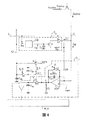
図1は、センサが感度の高い要素である赤外線カメラにより撮影された熱画像を表わす信号を生み出すために設計されたマトリックス・センサの、非常に概略的な図を示す。 FIG. 1 shows a very schematic diagram of a matrix sensor designed to produce a signal representing a thermal image taken by an infrared camera where the sensor is a sensitive element.
センサは、赤外線に対する感度の高い画素の行と列のマトリックスを含む。i番目の行とj番目の列の交点における画素Pi,jは、その行の全画素を結ぶ少なくとも1つの行導体Liに接続され、そしてその列の全画素を結ぶ列導体Cjに接続されることができる。 The sensor includes a matrix of rows and columns of pixels that are sensitive to infrared radiation. The pixel Pi, j at the intersection of the i-th row and the j-th column is connected to at least one row conductor Li that connects all the pixels in the row, and is connected to a column conductor Cj that connects all the pixels in the column. be able to.
行導体Liは画素の行をアドレス指定するために用いられる。行のアドレス指定回路ADLは、マトリックスの様々な行を連続的にアドレス指定し、i番目の行のアドレス指定は、その行の各画素の、当該画素に対応する列導体への有効な接続を生じる。各列の最下部には、アドレス指定された行の画素を経由して対応する列導体Cjに加えられる信号を読み取ることができる、j番目の列に対してCLjで示される読み取り回路がある。 Row conductor Li is used to address a row of pixels. The row addressing circuit ADL continuously addresses the various rows of the matrix, and the i-th row addressing determines the effective connection of each pixel in that row to the column conductor corresponding to that pixel. Arise. At the bottom of each column is a read circuit, denoted CLj, for the jth column that can read the signal applied to the corresponding column conductor Cj via the pixel in the addressed row.
マルチプレクサMUXは全ての読み取り回路CLjの出力を受け取り、そして各読み取り回路から生じる信号を出力SVに迅速に供給することを可能にする。例えばマルチプレクサMUXは、それぞれの列に対応する各信号の連続を、列の順番で出力SVに伝送する。この連続は、マトリックスの次の行がアドレス指定される期間中に、マトリックスの行のアドレス指定の最後に生み出された全ての信号が出力SVに伝送されるように、高速で伝送される。 The multiplexer MUX receives the outputs of all the reading circuits CLj and allows the signal resulting from each reading circuit to be quickly supplied to the output SV. For example, the multiplexer MUX transmits a series of signals corresponding to each column to the output SV in the column order. This sequence is transmitted at high speed so that during the period when the next row of the matrix is addressed, all signals produced at the end of the matrix row addressing are transmitted to the output SV.
図2は、感度の高い要素が放射要素である、個々の画素Pi,jの基本的な概略図を表わす。 FIG. 2 represents a basic schematic diagram of an individual pixel Pi, j, where the sensitive element is a radiating element.
放射要素は、値がその温度によって変化しかつ温度がとりわけ受けた赤外線放射の全体の流れによって変化する抵抗Rbにより表わされる。 The radiating element is represented by a resistance Rb whose value varies with its temperature and whose temperature varies among other things with the overall flow of infrared radiation received.
この後に続く全てにおいて、抵抗性の(又は容量性の)ハードウェア対象、又はこの対象のデジタル値(抵抗又はコンデンサ)を示すために、同じ名称(例えばRb)が使用されるであろう。 In all that follows, the same name (eg Rb) will be used to indicate a resistive (or capacitive) hardware object or a digital value (resistor or capacitor) of this object.
放射抵抗Rbは(マトリックスの全画素に共通の)基準電位VRに接続された第一端と、そのゲートが電位VGを受けるトランジスタT1のソースに接続された第二端とを有する。トランジスタT1のドレインはスイッチK1により、列導体Cjに接続されている。スイッチK1は行導体Liにより制御される。このスイッチは画素Pi,jと列導体Cjとの間の接続を構成又は切断する。この接続は、行Liがアドレス指定されたとき、スイッチK1が閉じることにより構成される。それは当該の行がアドレス指定されていないとき、スイッチK1の開放により切断される。 The radiation resistor Rb has a first end connected to a reference potential VR (common to all pixels of the matrix) and a second end whose gate is connected to the source of the transistor T1 receiving the potential VG. The drain of the transistor T1 is connected to the column conductor Cj by a switch K1. The switch K1 is controlled by the row conductor Li. This switch configures or disconnects the connection between the pixel Pi, j and the column conductor Cj. This connection is configured by closing switch K1 when row Li is addressed. It is disconnected by opening switch K1 when the row is not addressed.
列導体Cjの電位は基準電位VRよりも大きいため、及び電位VGは電位VRより少なくとも1つの値VTだけ大きく選ばれるため、トランジスタT1は行のアドレス指定の間は導通している。VTはトランジスタT1のしきい電圧であり、典型的には0.6Vである。 Since the potential of the column conductor Cj is greater than the reference potential VR and the potential VG is selected to be at least one value VT greater than the potential VR, the transistor T1 is conducting during row addressing. VT is the threshold voltage of transistor T1, typically 0.6V.
行Liのアドレス指定の間、抵抗Rbはその端子間にバイアス電圧Vpol=(VG−VT−VR)を受け、それゆえIm=(Vpol/Rb)であるような測定電流Imが渡るであろう。 During the addressing of the row Li, the resistor Rb will receive a bias voltage Vpol = (VG−VT−VR) across its terminals and therefore a measurement current Im such that Im = (Vpol / Rb) will pass. .
この電流は、トランジスタT1及びスイッチK1を用いて抵抗が接続される列導体Cjから取り出される。 This current is taken from the column conductor Cj to which the resistor is connected using the transistor T1 and the switch K1.
さらに、列の先頭に置かれた電源から、補償電流Icompが列の頭における列導体Cjに加えられる。列の最下部は、見られるように、基準電位Vrefに保たれる。所定の電圧Vcompが固定値の抵抗Rcompを用いて列導体に印加されるとき、補償電流は列の先頭においてIcomp=(Vcomp−Vref)/Rcompである。電流Icompは、所与の値の抵抗への所与の電圧の印加とは別の手段により生み出され得る。特に、それは既知の値Icompの電流源により固定され得る。 Further, a compensation current Icomp is applied to the column conductor Cj at the head of the column from the power supply placed at the head of the column. The bottom of the column is kept at the reference potential Vref as can be seen. When a predetermined voltage Vcomp is applied to the column conductor using a fixed value resistor Rcomp, the compensation current is Icomp = (Vcomp−Vref) / Rcomp at the beginning of the column. The current Icomp can be generated by means other than applying a given voltage to a given value resistor. In particular, it can be fixed by a current source of known value Icomp.
列の最下部において、列導体Cjはj番目の列と関連する測定回路CLjに接続されている。この回路は、列導体を通って列の最下部まで移動する残留電流Idを測定するであろう。残留電流Idは電流Icompと、列導体に画素が接続されているときにその画素によって取り出される測定電流Imとの差である。 At the bottom of the column, the column conductor Cj is connected to the measurement circuit CLj associated with the jth column. This circuit will measure the residual current Id traveling through the column conductor to the bottom of the column. The residual current Id is the difference between the current Icomp and the measured current Im taken out by the pixel when the pixel is connected to the column conductor.
測定される残留電流はそれゆえId=Icomp−Im、あるいは:
Id=Icomp−Vpol/Rb
である。
The measured residual current is therefore Id = Icomp−Im, or:
Id = Icomp−Vpol / Rb
It is.
読み取り回路CLjは、画素の行に対するこの測定のために予定された期間TLの間に残留電流を積分するであろう電流積分回路を備える。実際に、行Liは次に続く行のアドレス指定の前に、期間TLよりも僅かに長い期間アドレス指定されるが、しかし積分は期間TLの間のみ行なわれるであろう。例えば、64μsの行アドレス指定期間に対して、期間TLは50μsである。以下において、それが対象の行の場合、熱流の積分開始は時間0に起こり、積分の終了は時間TLに起こることが考えられるであろう。
The reading circuit CLj comprises a current integrating circuit that will integrate the residual current during the period TL scheduled for this measurement for the row of pixels. In fact, row Li is addressed for a period slightly longer than period TL before the addressing of the next succeeding line, but integration will only take place during period TL . For example, for a row addressing period of 64 μs, the period TL is 50 μs. In the following, if it is the row of interest, it will be considered that the start of heat flow integration occurs at
電流積分回路はCintの値の電流積分コンデンサを含み、それはこのコンデンサの端子に、残留電流Idの積分に比例する電圧Vciを供給する:

一例として、積分回路は、その非反転入力が基準電位Vrefを受け、その反転入力がそこから残留電流Idを受けるために列導体Cjに接続される演算増幅器AOPを備える。コンデンサCintは反転入力と演算増幅器AOPの出力との間に接続される。コンデンサの端子間に接続されたスイッチK2は、積分コンデンサCintを短絡させ、従ってその期間がTLである新たな積分の開始を定義するゼロ基準の瞬間において、このコンデンサの端子における電圧をゼロにすることを可能にする。このスイッチK2はそれゆえ、前の行をアドレス指定するための周期の終りに(又は行Liをアドレス指定するための周期の始めに)短時間(例えば4μsの間)閉じられ、そして各行に対して信号測定期間の始めを定義する時間0に開く。開くことにより、それはコンデンサへの積分の開始を可能にする。
As an example, the integrating circuit comprises an operational amplifier AOP that is connected to the column conductor Cj so that its non-inverting input receives a reference potential Vref and its inverting input receives a residual current Id therefrom. Capacitor Cint is connected between the inverting input and the output of operational amplifier AOP. A switch K2 connected between the terminals of the capacitor shorts the integrating capacitor Cint, so that at the zero reference instant defining the start of a new integration whose period is TL , the voltage at the terminal of this capacitor is zeroed. Make it possible to do. This switch K2 is therefore closed for a short time (for example for 4 μs) at the end of the cycle for addressing the previous row (or at the beginning of the cycle for addressing row Li) and for each row Open at
従来のやり方においては、フィードバック・コンデンサを経由してループを構成する、大きなゲイン及び大きな入力インピーダンスを有する演算増幅器AOPの存在のため、演算増幅器の反転入力に接続された列導体Cjの電位は、非反転入力に印加された電位Vrefに等しく留まると言うことができる。これが、列導体Cjの電位は基準電位Vrefに等しいということが上記に示されている理由である。 In the conventional way, due to the presence of the operational amplifier AOP having a large gain and large input impedance, which forms a loop via a feedback capacitor, the potential of the column conductor Cj connected to the inverting input of the operational amplifier is It can be said that it remains equal to the potential Vref applied to the non-inverting input. This is the reason described above that the potential of the column conductor Cj is equal to the reference potential Vref.
従って、積分期間の終りにおいて演算増幅器の出力Sに存在している電位VSは、電位Vrefと電位Vciとの合計である:
VS=Vref+Vci、あるいは
VS = Vref + Vci, or
増幅器の出力SはスイッチK3を経由して、機能が積分期間の終了後、及び次に続く行の読み込みの間に電圧VSの値を蓄えることである蓄電コンデンサCstに接続される。スイッチK3は、積分周期の終りに向かって短時間(例えば1μsの間)閉じられ、次に行に対する積分期間の終りを明らかにする時間TLに再び開放される。蓄電コンデンサCstの端子における電圧は、電圧VSが時間TLに到達する値に等しい値をとる。 The output S of the amplifier is connected via a switch K3 to a storage capacitor Cst whose function is to store the value of the voltage VS after the end of the integration period and during the reading of the next subsequent row. Switch K3 is closed for a short time (for example for 1 μs) towards the end of the integration period and then opened again at time TL , which reveals the end of the integration period for the row. The voltage at the terminal of the storage capacitor Cst takes a value equal to the value at which the voltage VS reaches the time TL .
蓄電コンデンサCstの端子における電圧は、(コンデンサの電荷の損失を防止するため)高インピーダンスの入力バッファ増幅器を用いて、マルチプレクサMUXのj番目のそれぞれの入力に印加される。マルチプレクサは、行Liに由来する画素の読み取りのために予定されたタイムスロットの間、すなわちその間に次に続くi+1番目の行がアドレス指定されるタイムスロットの間の任意の時間に、この電圧に対応する信号を伝送し得る。 The voltage at the terminal of the storage capacitor Cst is applied to each jth input of the multiplexer MUX using a high impedance input buffer amplifier (to prevent loss of charge on the capacitor). The multiplexer is set to this voltage at any time during the time slot scheduled for reading the pixels from row Li, i.e. during the time slot during which the next i + 1th row is addressed. A corresponding signal can be transmitted.
従って、この放射センサ構造において、マルチプレクサにより伝送されるであろう測定信号は次の量VSに比例する:
補償電流Icompは、残留電流Idが基準温度においてゼロであるように、Vcomp及びRcompに作用することにより選ばれることが望ましい。この基準温度は、例えば300Kの周囲温度である。従って300Kにおける周囲温度で、求められる公称の抵抗Rb0を有する理想的な画素に対して、パラメータVG、VR、及びIcompは、(VG−VT−VR)/Rb0=Icompであるように選ばれる。VTはこの技術により固定される。VG及びVR、及びIcompは自由に選定され得る。それゆえ、この理想的な画素はVrefを中心とする電圧VSにおいて信号を供給するであろう。それは300Kよりも高い温度にさらされるとき、Vrefよりも高く、より低い温度にさらされるとき、Vrefよりも低い。 The compensation current Icomp is preferably selected by acting on Vcomp and Rcomp so that the residual current Id is zero at the reference temperature. This reference temperature is, for example, an ambient temperature of 300K. Thus, for an ideal pixel with the required nominal resistance Rb0 at an ambient temperature of 300K, the parameters VG, VR, and Icomp are chosen such that (VG-VT-VR) / Rb0 = Icomp. The VT is fixed by this technique. VG and VR, and Icomp can be freely selected. This ideal pixel would therefore provide a signal at a voltage VS centered at Vref. It is higher than Vref when exposed to temperatures higher than 300K and lower than Vref when exposed to lower temperatures.
しかし、上述のように、Rbは大きな技術的ばらつき量であり、そして基準温度において、マトリックスの様々な画素に対する公称値Rb0とは非常に異なる値を持ち得る。 However, as described above, Rb is a large amount of technical variation and can have a value that is very different from the nominal value Rb0 for the various pixels of the matrix at the reference temperature.
ここで議論されているセンサ構造は1行ごとのアドレス指定を伴う構造である。画素は、行がアドレス指定されている間(典型的には64μs未満)のみ、バイアス電流により電力供給される。これは比較的大きなバイアス電流がそのとき抵抗Rbに与えられるためである。この電流の影響は、赤外線の照射に対する画素の露光により生成される、この電流の変化に比べて無視出来ないものである。例えば、抵抗の公称値は技術的なばらつきのために15%変化するが、これに対して抵抗は最小照度と最大照度の間で、受ける照度に応じて僅か1%しか変化しない。受けた照度に関する真の意味を有する画像をセンサにおいて得ることは、従ってこのばらつきによって著しく乱される。 The sensor structure discussed here is a structure with line-by-line addressing. The pixel is powered by the bias current only while the row is being addressed (typically less than 64 μs). This is because a relatively large bias current is then applied to the resistor Rb. The effect of this current is not negligible compared to this change in current generated by pixel exposure to infrared radiation. For example, the nominal value of the resistance varies by 15% due to technical variations, whereas the resistance varies by only 1% between the minimum and maximum illumination, depending on the illumination received. Obtaining an image at the sensor that has a true meaning for the received illuminance is thus significantly disturbed by this variation.
本発明は画素に特有の、トリマー・コンデンサに蓄えられるトリマー電圧値に反応するアナログ感度トリマー回路の助けにより、各画素を個々に修正することを提案する。この電圧値は、列の最下部で測定回路から情報の項目を受け取り、そして画素に特有のトリマー・コンデンサに電荷を供給する、フィードバック回路により供給される。調整値はとりわけ(しかし必須ではなく)、センサのマトリックスの一様な照度(望ましくは、例えば300Kの基準温度における照度)に基づく較正段階の間に供給され得る。 The present invention proposes to modify each pixel individually with the help of an analog sensitivity trimmer circuit that reacts to the trimmer voltage value stored in the trimmer capacitor, which is pixel specific. This voltage value is supplied by a feedback circuit that receives an item of information from the measurement circuit at the bottom of the column and supplies charge to the trimmer capacitor specific to the pixel. The adjustment value can be supplied, inter alia (but not essential), during a calibration phase based on the uniform illumination (desirably illumination at a reference temperature of, for example, 300K) of the sensor matrix.
従って、基準温度において抵抗Rbij0を有する画素Pi,jは、フィードバック・ループを経由して、それに特有の(しかしそれは必ずしも画素自体の中に地理的に位置する必要はない)トリマー・コンデンサの電圧の確立を可能にするであろう。このコンデンサに蓄えられる電圧の値は、基準熱流(又は温度)による照度に対し、列の最下部における測定回路の出力が全画素に対して同じ所定の値を有するような値であろう。フィードバック回路は自己修正式であり、トリマー・コンデンサにおける電圧は、例えそれらの抵抗Rbij0が基準熱流により生じる温度において互いに異なるとしても、全画素が一定時間の最後に、基準熱流に関して同じ測定信号を供給するように、徐々に確立される。 Thus, a pixel Pi, j having a resistance Rbij0 at the reference temperature is passed through a feedback loop to its own (but not necessarily geographically located within the pixel itself) trimmer capacitor voltage. It will be possible to establish. The value of the voltage stored in this capacitor will be such that the output of the measurement circuit at the bottom of the column has the same predetermined value for all pixels with respect to the illuminance due to the reference heat flow (or temperature). The feedback circuit is self-correcting so that the voltages at the trimmer capacitors provide the same measurement signal with respect to the reference heat flow at the end of a certain time, even though their resistances Rbij0 differ from each other at the temperature caused by the reference heat flow. To be established gradually.
本発明は、画素に特有のトリマー回路が次のパラメータの一つに対して働くことを提案する:
VG、Vref、TL、Icomp、望ましくは行のアドレス指定の間に放射抵抗のバイアス電圧を定義するVG。
The present invention proposes that a pixel specific trimmer circuit works for one of the following parameters:
VG, Vref, T L , Icomp, preferably VG which defines the bias voltage of the radiation resistor during row addressing.
トリマー回路を制御するトリマー・コンデンサを有するトリマー回路は、画素自体の中に必ずしも位置する必要はないが、画素内にトリマー・コンデンサが位置する実施形態は、画素の外にあるトリマー・コンデンサを有する実施形態に比べて有利である。 Trimmer circuits with a trimmer capacitor that controls the trimmer circuit need not necessarily be located within the pixel itself, but embodiments in which the trimmer capacitor is located within the pixel have a trimmer capacitor that is outside the pixel. This is advantageous compared to the embodiment.
この主題において、各画素における電圧VGに対して措置が講じられる実施形態は特に有利である。そして今ここで図3を参照して説明されるのは、その実施形態である。マトリックス・ネットワークの全体構成は図1及び図2と同じであり、本発明によって加えられる特有の特徴は以下に示されるであろう。図2と同じ参照符号を持つ要素は図3においても同じである。 In this subject, embodiments in which measures are taken for the voltage VG at each pixel are particularly advantageous. And what is now described with reference to FIG. 3 is an embodiment thereof. The overall configuration of the matrix network is the same as in FIGS. 1 and 2, and the specific features added by the present invention will be shown below. Elements having the same reference numerals as in FIG. 2 are the same in FIG.
画素に特有な、そして画素内に位置するトリマー・コンデンサはCaで示される。トリマー回路は単に、図2において既に存在するトランジスタT1から成る。そのトランジスタはフォロワとして組み込まれ、かつそのソースにおける電圧が、そのゲート上に存在している電圧に、1つのしきい電圧降下VT以内まで直接的に追従するため、それはトリマー回路の役割を演じる。このゲート電圧はここで、トランジスタT1のゲートとゼロ電位のアースとの間に取り付けられた、トリマー・コンデンサCaにおいて存在するトリマー電圧である。トランジスタT1のゲート−基板コンデンサは、さらにトリマー・コンデンサCaの一部分であると考えられ得る。 The trimmer capacitor that is pixel specific and located within the pixel is denoted Ca. The trimmer circuit simply consists of the transistor T1 already present in FIG. The transistor is incorporated as a follower, and it plays the role of a trimmer circuit because the voltage at its source directly follows the voltage present on its gate to within one threshold voltage drop VT. This gate voltage is here the trimmer voltage present in the trimmer capacitor Ca, which is mounted between the gate of the transistor T1 and the zero potential ground. The gate-substrate capacitor of transistor T1 can also be considered to be part of the trimmer capacitor Ca.
フォロワ・トランジスタのトリマー電圧、又はゲート電圧VGは、上記に説明した如く放射抵抗のバイアス電圧を直接決定する:
Vpol=VG−VT−VR、
ここでVGは各画素に対して個々に変えられ得る電圧である。
The follower transistor trimmer voltage or gate voltage VG directly determines the bias voltage of the radiation resistance as described above:
Vpol = VG-VT-VR,
Here, VG is a voltage that can be individually changed for each pixel.
図3は、各々がフォロワ・トランジスタによりバイアスをかけられた放射抵抗を含む、2つの隣接する画素Pi,j及びPi−1,jを表わす。放射抵抗Rbはフォロワ・トランジスタのソースと、全画素に共通の基準電圧VRにおける点との間に接続される。トランジスタのしきい電圧VTは全画素に対して同一と考えられ得る。 FIG. 3 represents two adjacent pixels Pi, j and Pi-1, j, each including a radiation resistor biased by a follower transistor. The radiation resistor Rb is connected between the source of the follower transistor and a point at the reference voltage VR common to all pixels. The threshold voltage VT of the transistor can be considered the same for all pixels.
コンデンサCaにおいて適切なトリマー電圧を確立するために用いられるフィードバック回路は、機能が、行の読み取り後にトリマー・コンデンサに対し、画素の感度が全画素に対して求められる公称の感度と異なるときにより大きい、プラス又はマイナスの符号付きの電荷量を加えることである、電荷増加回路CQを含む。電荷の量はプラス又はマイナスであり、それは以前にトリマー・コンデンサに蓄えられた電荷量に加えられる。このように追加される電荷量のプラス又はマイナスの符号は、画素の感度が求められる公称の感度に近づく傾向のものである。 The feedback circuit used to establish the proper trimmer voltage at the capacitor Ca is greater when the function is different from the nominal sensitivity required for all pixels for the trimmer capacitor after reading the row. , Including a charge increasing circuit CQ, which is to add a plus or minus signed amount of charge. The amount of charge is positive or negative and it is added to the amount of charge previously stored in the trimmer capacitor. The plus or minus sign of the added charge amount tends to approach the nominal sensitivity for which the pixel sensitivity is required.
増加回路CQは、追加又は減算されるべき電荷の量を決定するために、行読み取りの最後に、従って読み取りの終了を定義する時間TLの後に、読み取り回路CLjによって集められた電圧VSのレベルを、制御として用いる。所与の照度に対して画素の感度を表わすのは、具体的にこのレベルである。 The increment circuit CQ determines the level of the voltage VS collected by the read circuit CLj at the end of the row read and thus after the time TL defining the end of the read to determine the amount of charge to be added or subtracted. Is used as a control. It is this level that specifically represents the sensitivity of the pixel for a given illuminance.
しかしながら、コンデンサCaにおけるトリマー電圧のレベルを即座にではなく徐々に確立するために、非常に小さい増分によって、次のやり方でその方法が進むことが望ましい:
行の読み取りの最後に蓄電コンデンサCstに蓄えられる電圧レベルVSは、以下で説明され、この場合Vgrisと呼ばれるであろう平均電圧レベルに予充電される、大形のコンデンサCdivに印加される。VgrisはVrefと等しいことが望ましい。予充電は電流積分のため、期間TLの最後に短いタイムスロットの間に行なわれることが望ましい。このタイムスロットの間、スイッチK5はコンデンサCdivを基準電圧Vgrisに接続する。スイッチK5の制御は、実際にはスイッチK3の制御と同時である。
However, in order to establish the level of the trimmer voltage at capacitor Ca gradually rather than immediately, it is desirable that the method proceed in the following manner with very small increments:
The voltage level VS stored in the storage capacitor Cst at the end of a row read is applied to a large capacitor Cdiv, which will be described below and in this case will be precharged to an average voltage level that will be referred to as Vgris. Vgris is preferably equal to Vref. The precharge is preferably performed during a short time slot at the end of the period TL for current integration. During this time slot, the switch K5 connects the capacitor Cdiv to the reference voltage Vgris. The control of the switch K5 is actually the same as the control of the switch K3.
コンデンサCdivの予充電後に、蓄電コンデンサCstの端子に存在する電圧はこのコンデンサに印加され、電圧は画素読み取りの最後における出力電圧VSを表わす。スイッチK4は、コンデンサCstをコンデンサCdivに接続するために用いられる。スイッチK4は短時間閉じられ、この閉塞はスイッチK5の再開放の後のみに実施され得る。 After precharging the capacitor Cdiv, the voltage present at the terminal of the storage capacitor Cst is applied to this capacitor, and the voltage represents the output voltage VS at the end of pixel reading. The switch K4 is used to connect the capacitor Cst to the capacitor Cdiv. Switch K4 is closed for a short time and this blockage can only be implemented after reopening of switch K5.
コンデンサCdivの役割は、予充電のために当初VgrisであるコンデンサCdivの端子の電圧が、VSとVgrisとの間の差の一部分だけ増加するように、一種の容量性の分割器を構成することである。より正確には、電圧はVgrisから
Vgris+(VS−Vgris)・Cst/(Cst+Cdiv)
に変化する。
The role of the capacitor Cdiv is to configure a kind of capacitive divider so that the voltage at the terminal of the capacitor Cdiv, which is initially Vgris, for precharging increases by a fraction of the difference between VS and Vgris. It is. More precisely, the voltage is from Vgris Vgris + (VS−Vgris) · Cst / (Cst + Cdiv)
To change.
それゆえ、電圧VSがVgrisに等しい場合、予充電されたコンデンサCdivに対する電圧の増減はない。しかし電圧VSがVgrisよりも高いか低い場合、コンデンサCdivの端子における電圧は、VSとVgrisとの差の一部分だけ僅かに変化する。 Therefore, when the voltage VS is equal to Vgris, there is no increase or decrease in voltage relative to the precharged capacitor Cdiv. However, if the voltage VS is higher or lower than Vgris, the voltage at the terminal of the capacitor Cdiv changes slightly by a fraction of the difference between VS and Vgris.
コンデンサCdivの端子における電圧は、(VS−Vgris)・Cst/(Cst+Cdiv)の差に比例して、すなわちコンデンサCdivに対して丁度なされた電圧の小さな増加又は減少に比例して、トリマー・コンデンサCaの電荷を変更するために、次に制御電圧として電荷増加回路CQに印加される。図3において、電荷増加回路は各画素内に地理的に位置しているとして表わされる。全画素に共通の増加回路を想定することもまた可能である。 The voltage at the terminal of the capacitor Cdiv is proportional to the difference of (VS−Vgris) · Cst / (Cst + Cdiv), ie proportional to the small increase or decrease of the voltage just made to the capacitor Cdiv, the trimmer capacitor Ca Is then applied to the charge increasing circuit CQ as a control voltage. In FIG. 3, the charge augmentation circuit is represented as being geographically located within each pixel. It is also possible to envisage an increasing circuit common to all pixels.
コンデンサCaの電荷の変動は当然、画素の感度を求められる公称値に至らせる傾向がある方向になされる。 Naturally, the fluctuation of the electric charge of the capacitor Ca tends to bring the pixel sensitivity to the required nominal value.
画素の感度の較正は従って、アナログ電圧VSを恒久的に測定することにより、そしてトリマー回路が、所与の照度に対して画素により供給される電圧の差VS−Vgrisを少ない割合だけ変更するように、トリマー・コンデンサに少量の電荷を加えることにより望ましくは実施される。ここでVgrisは、平均照度に対して求められる感度を有する画素によって供給される、アナログ電圧に相当する基準電圧値である。「少ない割合」とは、較正が一様な光源に基づき特定の較正段階において行なわれる場合には、10%未満の割合を意味し、較正が一様な光源無しで、使用中にそれ自体で行なわれる場合には、1%以下の割合を意味しなければならない。 The calibration of the pixel sensitivity thus allows the analog voltage VS to be measured permanently and the trimmer circuit to change the voltage difference VS-Vgris supplied by the pixel by a small percentage for a given illuminance. In addition, this is preferably accomplished by applying a small amount of charge to the trimmer capacitor. Here, Vgris is a reference voltage value corresponding to an analog voltage supplied by a pixel having a sensitivity required for the average illuminance. “Small percentage” means a percentage of less than 10% if calibration is performed at a specific calibration stage based on a uniform light source, and the calibration itself is in use without a uniform light source. If done, it should mean a proportion of 1% or less.
コンデンサCdivは、その電圧VSが丁度測定された画素の電荷増加回路に接続されなければならない。このため、コンデンサCdivは全ての画素の列(j番目の列)に共通の帰路導体Crにより、画素に接続され得る。 Capacitor Cdiv must be connected to the charge increase circuit of the pixel whose voltage VS has just been measured. For this reason, the capacitor Cdiv can be connected to the pixel by a return conductor Cr common to all pixel columns (jth column).
画素Pi,jの増加回路CQは、導体Crが他の画素の測定に関する情報の項目を搬送する間ではなく、この画素に関する電圧情報の項目を搬送する間のみ、電荷をコンデンサCaに移動させなければならない。スイッチK6が回路CQの入力を導体Crに接続し、このスイッチが開放された後に行のアドレス指定期間の間のみ閉じられる理由はこれである。 The increase circuit CQ of the pixel Pi, j must move the charge to the capacitor Ca only while the conductor Cr carries the item of information relating to the measurement of the other pixel, but not while carrying the item of voltage information relating to this pixel. I must. This is why switch K6 connects the input of circuit CQ to conductor Cr and is closed only during the row addressing period after the switch is opened.
勿論、導体Crに電圧(VS−Vgris)・Cst/(Cst+Cdiv)を生じさせるのが画素Pi,jである場合、i番目の行のアドレス指定の最後にこの電圧を受けるのは画素Pi,jであって、前の画素あるいは次の画素ではないことに注意が払われなければならない。 Of course, if it is the pixel Pi, j that produces the voltage (VS−Vgris) · Cst / (Cst + Cdiv) on the conductor Cr, it is the pixel Pi, j that receives this voltage at the end of the addressing of the i th row. Note that it is not the previous or next pixel.
信号のシーケンスによれば、2つの可能な仮定が存在する:
−第1の仮定において、行Liのアドレス指定はコンデンサCintにおける電流の積分の終了を定義する時間TLに終わる。i+1番目の新たな行のアドレス指定は、この瞬間に始まる。電圧(VS−Vgris)・Cst/(Cst+Cdiv)は、期間TLの後にのみ帰路導体Crにおいて得られる。この仮定において、図3に示すように対応するスイッチK6はi番目の行をアドレス指定する制御ではなく、i+1番目の行をアドレス指定するための制御によって閉じられる。それゆえ、次に続く行のアドレス指定が既に始まっていても、その画素の読み取りから確立される情報の項目を受け取るのは、実際に当の画素Pi,jである。
−第2の仮定において、スイッチK6がi+1番目の導体によってではなく、画素Pi,jに対応する行導体Liによってそのとき制御され得るように、次の行のアドレス指定に移る前に電圧を帰路導体Crに印加するための時間が取られる。この第2の仮定において、帰路導体Crにおける電圧を構成するために用いられる、コンデンサCstと同じ電圧VSを受ける補助の蓄電コンデンサC’stを備えることが望ましい。
According to the sequence of signals, there are two possible assumptions:
In the first assumption, the addressing of the row Li ends at a time TL that defines the end of the integration of the current in the capacitor Cint. The addressing of the i + 1th new row begins at this moment. The voltage (VS−Vgris) · Cst / (Cst + Cdiv) is obtained at the return conductor Cr only after the period TL . Under this assumption, as shown in FIG. 3, the corresponding switch K6 is closed by the control for addressing the i + 1 th row, not by the control for addressing the i th row. Therefore, even if the addressing of the next succeeding row has already begun, it is actually the current pixel Pi, j that receives the item of information established from the reading of that pixel.
In the second assumption, the voltage is returned before moving to the next row addressing so that the switch K6 can now be controlled by the row conductor Li corresponding to the pixel Pi, j, not by the i + 1 th conductor. Time is applied to apply to the conductor Cr. In this second assumption, it is desirable to have an auxiliary storage capacitor C′st that receives the same voltage VS as the capacitor Cst, which is used to construct the voltage at the return conductor Cr.
第1の仮定は図3の線図において用いられている。第2の仮定は図4の線図において用いられている。図4において、図3のものと共通の要素は同じ参照符号により示されている。 The first assumption is used in the diagram of FIG. The second assumption is used in the diagram of FIG. 4, elements common to those in FIG. 3 are indicated by the same reference numerals.
図3において、フィードバック・ループはそれゆえ電流積分回路の出力とトリマー・コンデンサとの間に:
−両方が同時に読み取り回路CLjの部分を形成する、蓄電コンデンサCst及びスイッチK3と、
−コンデンサCdiv、電圧VgrisをリセットするスイッチK5、初期設定後にその電圧の変更を可能にするスイッチK4、関連する画素への情報項目を伝送する帰路導体Cr(列あたり1つ)と、
−画素内に地理的に位置するスイッチK6及び電荷増加回路CQと
を備える。
In FIG. 3, the feedback loop is therefore between the output of the current integrator and the trimmer capacitor:
The storage capacitor Cst and the switch K3, both of which form part of the reading circuit CLj at the same time;
A capacitor Cdiv, a switch K5 that resets the voltage Vgris, a switch K4 that allows the voltage to be changed after initialization, a return conductor Cr (one per column) that transmits information items to the associated pixel;
A switch K6 and a charge increasing circuit CQ, which are geographically located in the pixel.
図4において、帰路導体Crと画素Pi,jとの間の接続は、画素Pi+1,jに対応する行Li+1のアドレス指定によってではなく、画素Pi,jに対応する行Liのアドレス指定の間に閉じられるスイッチK6によってなされる。その上、図3においてコンデンサCstがマルチプレクサに送られる電圧VSを蓄え、そしてコンデンサCdivの電圧レベルを制御する二重の役割を果たした一方で、これら2つの役割はここでは分離され、第2の役割は補助コンデンサC’stに割り当てられている。 In FIG. 4, the connection between the return conductor Cr and the pixel Pi, j is not based on the addressing of the row Li + 1 corresponding to the pixel Pi + 1, j, but between the addressing of the row Li corresponding to the pixel Pi, j. This is done by the switch K6 being closed. Moreover, in FIG. 3, the capacitor Cst stores the voltage VS that is sent to the multiplexer and serves the dual role of controlling the voltage level of the capacitor Cdiv, while these two roles are separated here, the second The role is assigned to the auxiliary capacitor C′st.
コンデンサC’stは、増幅器AOPの出力とコンデンサC’stとの間に接続されたスイッチK7のおかげで、期間TLの終りに短時間にわたり電圧VSにおいて充電され得る。スイッチK7はスイッチK3及びスイッチK5と同時に作動する。スイッチK4はもはやコンデンサCstとコンデンサCdivとの間には接続されないが、しかしコンデンサC’stとコンデンサCdivとの間に接続される。コンデンサCstはそのときコンデンサC’stよりもずっと高い値を持ち得る。一例として、通常の使用における画素のレベルを蓄える主要な役割と、帰路導体Crに対してトリマー電圧を発生する補助的役割の両方を満たし得るために、図3の線図においてCstが代わりに0.1ピコファラッドの値を有する一方で、図4においてCstは1ピコファラッドの値、そしてC’stは0.1ピコファラッドの値を有する。 Capacitor C′st can be charged at voltage VS for a short time at the end of period TL , thanks to switch K7 connected between the output of amplifier AOP and capacitor C′st. Switch K7 operates simultaneously with switch K3 and switch K5. Switch K4 is no longer connected between capacitor Cst and capacitor Cdiv, but is connected between capacitor C'st and capacitor Cdiv. Capacitor Cst can then have a much higher value than capacitor C′st. As an example, Cst is instead 0 in the diagram of FIG. 3 to satisfy both the primary role of storing pixel levels in normal use and the auxiliary role of generating a trimmer voltage for the return conductor Cr. 4 has a value of 1 picofarad, while Cst has a value of 1 picofarad and C′st has a value of 0.1 picofarad.
図4の線図において、コンデンサCaに対してトリマー電圧VGを発生するために用いられるフィードバック回路は、本質的に:
−追加のコンデンサC’st及び、画素から発生する出力電圧VSをそこに印加することを可能にするスイッチK7と、
−コンデンサCdiv、電圧Vgrisに対してそれをリセットするスイッチK5、初期設定後にその電圧の変更を可能にするスイッチK4、関連する画素への情報項目を伝送する帰路導体Cr(列あたり1つ)と、
−画素内に位置するスイッチK6及び電荷増加回路CQと
を備える。
In the diagram of FIG. 4, the feedback circuit used to generate the trimmer voltage VG for the capacitor Ca is essentially:
An additional capacitor C′st and a switch K7 that allows an output voltage VS generated from the pixel to be applied thereto;
A capacitor Cdiv, a switch K5 that resets it to the voltage Vgris, a switch K4 that allows the voltage to be changed after initialization, a return conductor Cr (one per column) that transmits information items to the associated pixel, ,
A switch K6 and a charge increasing circuit CQ located in the pixel;
図3の線図あるいは図4の線図を通じ、一様な照度を有する数十の画像にわたって続く較正段階の間、VSとVgrisとの間で見られる差を補償するため、それらのトリマー・コンデンサCaが漸進的に充電又は放電する如く、徐々に、全画素はVgrisに等しい同一の電圧レベルVSを漸進的に供給するであろうことが理解される。容量性の分割比Cst/(Cst+Cdiv)又はC’st/(C’st+Cdiv)が小さい程、トリマー電圧に到達する時定数が長くなる。 In order to compensate for the difference seen between VS and Vgris during the calibration phase that continues over several tens of images with uniform illumination through the diagram of FIG. 3 or the diagram of FIG. It is understood that gradually all pixels will progressively supply the same voltage level VS equal to Vgris as Ca is progressively charged or discharged. The smaller the capacitive division ratio Cst / (Cst + Cdiv) or C′st / (C′st + Cdiv), the longer the time constant to reach the trimmer voltage.
電圧Vgrisは電荷増加回路CQの構成によって選択される。具体的に、後者の機能は電圧(VS−Vgris)・Cst/(Cst+Cdiv)を(VS−Vgris)に比例する電荷の量dQへと変換することである。例えば、電圧/充電の変換を行なう、この電荷増加変換回路が対称なやり方で構成され、0Vにおける低い供給電圧とVddにおける高い供給電圧との間で給電されるのを認めることによって、VgrisがVdd/2に等しく選ばれる場合に、VS−Vgrisに比例する電荷量の生成を行なうことが容易に可能であろうと理解される。これが当てはまる場合(しかしそれは必須ではない)、Vgris=Vdd/2が選択され、スイッチK5は例えば電位0とVddとの間に置かれた抵抗の分割ブリッジにより得られる、電圧Vdd/2に接続されるであろう。
The voltage Vgris is selected depending on the configuration of the charge increasing circuit CQ. Specifically, the latter function is to convert the voltage (VS−Vgris) · Cst / (Cst + Cdiv) into an amount of charge dQ proportional to (VS−Vgris). For example, by allowing this charge-increasing conversion circuit, which performs voltage / charge conversion, to be configured in a symmetric manner and powered between a low supply voltage at 0V and a high supply voltage at Vdd, Vgris is Vdd It will be understood that it would be readily possible to generate a charge quantity proportional to VS-Vgris when chosen equal to / 2. If this is the case (but it is not essential), Vgris = Vdd / 2 is selected, the switch K5 is connected to the voltage Vdd / 2, for example obtained by a resistive dividing bridge placed between the
図3と4の説明の中で、画素の感度微調整は放射抵抗の制御用トランジスタの電圧VGの個々のトリミングにより行なわれ、そしてこのトリミングは、Vpol=VG−VT−VRであるため、行の読み取り中に画素に印加されるバイアスVpolを調整することを意味するのが見られる。VT及びVRはこれらの実施形態において固定された量である。 In the description of FIGS. 3 and 4, the fine adjustment of the sensitivity of the pixel is performed by individual trimming of the voltage VG of the radiation resistance control transistor, and this trimming is Vpol = VG−VT−VR. It can be seen that it means adjusting the bias Vpol applied to the pixel during the reading of. VT and VR are fixed amounts in these embodiments.
1つの変形として、関連する画素のi番目に相当する行のアドレス指定中に、列導体に加えられる補償電流Icompの値を制御するため、トリマー電圧が使用されるように備えることもまた可能である。例えばフィードバック回路により得られたトリマー電圧によって制御される電流の、アースへの迂回路を画素内に備えることが可能である。 As a variant, it can also be provided that a trimmer voltage is used to control the value of the compensation current Icomp applied to the column conductor during the addressing of the i th corresponding row of the relevant pixel. is there. For example, it is possible to provide a detour in the pixel for the current controlled by the trimmer voltage obtained by the feedback circuit to ground.
同様に、基準電圧Vrefがフィードバック回路により変更されることが可能であり、これは各画素に対して行なわれ得る。しかしこの場合、Vrefの電圧は地理的に画素内へ伝えられないため、フィードバック回路は画素に戻らないことが理解される。これは、センサ自体のマトリックスの外に、図3及び図4のトリマー・コンデンサCaが電圧Vpolに対して作用するのと同じように、基準電圧Vrefに対して作用できるトリマー・コンデンサのネットワークの備えが必要であることを意味する。このトリマブル・コンデンサのネットワークは、較正動作と通常使用の2つの動作がはっきりと区別できる場合に、これら較正動作中及び通常使用中の双方の間に、特定のトリマブル・コンデンサを所与の画素に対応させることが出来るように、画素の行と同時にアドレス指定され得る。 Similarly, the reference voltage Vref can be changed by a feedback circuit, which can be done for each pixel. However, in this case, it is understood that the feedback circuit does not return to the pixel because the voltage of Vref is not geographically transmitted into the pixel. In addition to the matrix of the sensor itself, this provides for a network of trimmer capacitors that can act on the reference voltage Vref in the same way that the trimmer capacitor Ca of FIGS. 3 and 4 acts on the voltage Vpol. Means that is necessary. This trimmable capacitor network allows a particular trimmable capacitor to be applied to a given pixel during both calibration and normal use, when the calibration and normal use are clearly distinguishable. It can be addressed simultaneously with a row of pixels so that it can be matched.
別の可能性は、基準照度に対する画素の実視感度が全画素に関して同じであるように、各画素が調整された積分期間を持つために、積分期間TLに対して作用することである。具体的には、既に見られたように信号レベルVSは積分期間TLに直接依存する。ここで再び、放射マトリックスの行と同時にアドレス指定され得る、画素外のトリマブル・コンデンサのネットワークを備えることが必要であり、各コンデンサはアドレス指定された各行に対し(そしてまた勿論その行のアドレス指定の間に、考えられる各列に対し)、特有の積分時間を調整するために読み取り回路CLjに対して作用することを可能にする。 Another possibility is to act on the integration period TL so that each pixel has an adjusted integration period so that the real visibility of the pixel relative to the reference illuminance is the same for all pixels. Specifically, as already seen, the signal level VS is directly dependent on the integration period TL . Here again, it is necessary to have a network of off-pixel trimmable capacitors that can be addressed simultaneously with the rows of the emission matrix, each capacitor for each addressed row (and of course also addressing that row) (For each possible column), it is possible to act on the reading circuit CLj to adjust the specific integration time.
最後に、基準の熱輝度画像を有する較正段階は必須ではなく、そして較正は単に、全画素に対して同一の平均感度値に相当する安定した値を、徐々にトリマー電圧に取らせることにあり得ると記憶されるべきである。画素が平均の基準Vgrisと異なる信号を供給するとき、小さなプラス又はマイナス符号付きの電荷増分がトリマー・コンデンサに加えられる、上記に示されている再帰的手法は、多数の画像に対して、全画素が熱輝度の同一の統計的分布を見なければならないことが考慮されるとき、とりわけ平均感度の周りで全画素の安定へと徐々に導く。この自動的較正方法が用いられる場合、時定数は非常に大(数百の画像、すなわち少なくとも数秒)でなければならず、その結果として容量性の分割比率Cst/(Cst+Cdiv)又はC’st/(C’st+Cdiv)は、非常に小(望ましくは0.01以下)でなければならない。それは事実上、画素の各々の新たな照度が、コンデンサCaに蓄えられたトリマー電圧VGを非常に僅かだけ変更するための条件である。 Finally, a calibration step with a reference thermo-brightness image is not essential, and the calibration is simply to have the trimmer voltage gradually take a stable value corresponding to the same average sensitivity value for all pixels. Should be remembered as you get. When the pixel provides a signal different from the average reference Vgris, a small plus or minus signed charge increment is added to the trimmer capacitor. When considering that a pixel must see the same statistical distribution of thermal brightness, it gradually leads to the stability of all pixels, especially around the average sensitivity. When this automatic calibration method is used, the time constant must be very large (hundreds of images, ie at least a few seconds), resulting in a capacitive split ratio Cst / (Cst + Cdiv) or C′st / (C′st + Cdiv) must be very small (preferably 0.01 or less). In effect, this is a condition for the new illuminance of each pixel to change the trimmer voltage VG stored in the capacitor Ca very slightly.
混合した方法、すなわち、恒久的な自己修正を伴う使用の段階が後に続く、マトリックス全体を一様な熱流にさらす最初の較正段階が採用される場合、望ましくは(例えば10〜50画像の期間の、較正におけるより短い段階と、例えば100〜500画像の、使用におけるより長い段階の)2つの段階の間に、時定数を変更するための手段を備えることが必要である。この変更は、コンデンサC’stを異なる値の別のコンデンサにより置き換えることによってなされ得る。 If a mixed method is employed, i.e. an initial calibration step that exposes the entire matrix to a uniform heat flow followed by a step of use with permanent self-correction, it is desirable (e.g. for a period of 10-50 images). It is necessary to provide a means for changing the time constant between two stages, a shorter stage in calibration and a longer stage in use, eg 100-500 images. This change can be made by replacing the capacitor C'st with another capacitor of a different value.
一様な基準熱流にさらすことによる較正方法が(望ましくは相当に短い(1秒未満又は数十の画像の)時定数を伴う)使用される唯一のものである場合は、較正段階においてフィードバック・ループの操作を可能にし、その後の使用段階においてそれを回避する手段(図3及び図4には図示せず)を備えることが必要である。較正段階の間に生成されるトリマー電圧は、新たな較正段階まで、使用段階の間中コンデンサCaに保持される。 If the calibration method by exposure to a uniform reference heat flow is the only one used (desirably with a time constant (less than 1 second or tens of images)), feedback It is necessary to provide means (not shown in FIGS. 3 and 4) to allow the operation of the loop and to avoid it in the subsequent use phase. The trimmer voltage generated during the calibration phase is held in the capacitor Ca throughout the use phase until a new calibration phase.
ADL 行のアドレス指定回路
Cj 列導体
Li 行導体
Pi,j 画素
CLj 読み取り回路、測定回路
MUX マルチプレクサ
SV 出力
Vcomp 所定の電圧
Rcomp 固定値の抵抗
Icomp 補償電流
VG トリマー電圧、電位、電圧、放射抵抗のバイアス電圧、パラメータ、ゲート電圧
T1 トランジスタ、トリマー回路
K1 スイッチ
VT トランジスタ(T1)のしきい電圧
Vpol バイアス電圧
Im 測定電流
Rb (放射)抵抗
Rb0 公称の抵抗
Id 残留電流
K2 スイッチ
VR (基準)電位、固定電位、パラメータ
Vci 電圧、電位
TL 期間、時間、積分期間
K3 スイッチ
S (演算)増幅器の出力
Cst (主要な)(蓄電)コンデンサ
VS アナログ(出力)電圧、出力電圧、電圧、信号情報、出力情報、信号レベル、電位
AOP (演算)増幅器
Vref (基準)電位、基準電圧
Pi−1,j 画素
Li−1 画素Pi−1,jに対応する行
Li+1 画素Pi+1,jに対応する行
K4 スイッチ
K5 スイッチ
K6 スイッチ
CQ (電荷)増加回路、トリマー・コンデンサの電圧を使用段階において増加させるための手段
Ca (トリマー・)コンデンサ
Cr (帰路)導体、列導体
Vgris 基準電圧(値)、所定の電圧値
Cdiv (基準)コンデンサ
Cint (電流)積分コンデンサ
Ta 期間
C’st (補助)コンデンサ、補助の蓄電コンデンサ、追加のコンデンサ
K7 スイッチ
ADL row addressing circuit Cj column conductor Li row conductor Pi, j pixel CLj reading circuit, measurement circuit MUX multiplexer SV output Vcomp predetermined voltage Rcomp fixed value resistor Icomp compensation current VG trimmer voltage, potential, voltage, radiation resistance bias Voltage, Parameter, Gate Voltage T1 Transistor, Trimmer Circuit K1 Switch VT Transistor (T1) Threshold Voltage Vpol Bias Voltage Im Measurement Current Rb (Radiation) Resistance Rb0 Nominal Resistance Id Residual Current K2 Switch VR (Reference) Potential, Fixed Potential , Parameter Vci voltage, potential TL period, time, integration period K3 switch S (operation) amplifier output Cst (main) (storage) capacitor VS analog (output) voltage, output voltage, voltage, signal information, output information, Signal , Potential AOP (operation) amplifier Vref (reference) potential, reference voltage Pi-1, j pixel Li-1 row corresponding to pixel Pi-1, j row Li + 1 row corresponding to pixel Pi + 1, j K4 switch K5 switch K6 switch CQ (charge) increasing circuit, means for increasing the voltage of the trimmer capacitor at the use stage Ca (trimmer) capacitor Cr (return) conductor, column conductor Vgris reference voltage (value), predetermined voltage value Cdiv (reference) Capacitor Cint (current) integration capacitor Ta period C'st (auxiliary) capacitor, auxiliary storage capacitor, additional capacitor K7 switch
Claims (13)
行ごとにアドレス指定され得る画素の行と列のマトリックスと、前記行がアドレス指定される時に、前記列の画素(Pi,j)から発生する電流を連続的に受けるため、画素の列に各々が関連する一連の信号読み取り回路(CLj)とを備え、前記マトリックスの各画素が、画素により受け取られる熱流に値Rbが依存する放射抵抗を含み、この抵抗がVpolの値のバイアス電圧によりバイアスをかけられ、前記読み取り回路が、前記放射抵抗を通って流れる電流Vpol/Rbと補償電流との間の差を、積分コンデンサへと組み入れるための積分回路を備える、マトリックス熱画像センサにおいて、
センサが、前記マトリックスの各列に対して、
前記列の画素に共通な前記読み取り回路の前記積分コンデンサから始まり、トリマー・コンデンサ内に前記画素特有のトリマー電圧(VG)を蓄えるための、各画素に特有で前記画素内に位置するトリマー・コンデンサ(Ca)で終わるフィードバック・ループ(K4,Cdiv,Cr,K6,CQ)と、
前記画素が属する行が読み取られるとき、前記放射抵抗の前記バイアス電圧を変更するためにこのトリマー電圧に応答して作用する、前記画素内に位置するアナログ感度トリマー回路(T1)と、
を備え、フィードバック・ループが、
前記読み取り回路(CLj)により供給されるアナログ電圧VSを蓄えるための、蓄電コンデンサ(Cst,C’st)と、
当該の列の前記画素に共通の基準コンデンサ(Cdiv)と、
所定の電圧値(Vgris)でこの基準コンデンサを予充電するための手段と、
この基準コンデンサに、この所定の電圧と前記読み取り回路により供給される前記アナログ電圧(VS)との差を表わす電荷を加えるための手段と、
前記基準コンデンサの端子における前記アナログ電圧に応じて、前記トリマー・コンデンサの端子における電圧を増加又は減少させるように、前記トリマー・コンデンサに対応する電荷を加えるための手段と
を含むことを特徴とする、マトリックス熱画像センサ。 A matrix thermal image sensor,
A matrix of rows and columns of pixels that can be addressed per row, and each column of pixels to continuously receive current generated from the pixels (Pi, j) of the column when the row is addressed And a series of signal reading circuits (CLj) associated with each pixel of the matrix, each pixel including a radiation resistance whose value Rb depends on the heat flow received by the pixel, which is biased by a bias voltage of a value of Vpol. In a matrix thermal image sensor, wherein the read circuit comprises an integrating circuit for incorporating the difference between the current Vpol / Rb flowing through the radiation resistor and the compensation current into an integrating capacitor,
For each column of the matrix, a sensor
A trimmer capacitor unique to each pixel and located within the pixel for storing the pixel-specific trimmer voltage (VG) in the trimmer capacitor, starting with the integrating capacitor of the read circuit common to the pixels of the column A feedback loop (K4, Cdiv, Cr, K6, CQ) ending with (Ca);
An analog sensitivity trimmer circuit (T1) located within the pixel that acts in response to the trimmer voltage to change the bias voltage of the radiation resistance when the row to which the pixel belongs is read;
With a feedback loop
A storage capacitor (Cst, C′st) for storing the analog voltage VS supplied by the reading circuit (CLj);
A reference capacitor (Cdiv) common to the pixels of the column;
Means for precharging the reference capacitor with a predetermined voltage value (Vgris);
Means for adding to the reference capacitor a charge representative of the difference between the predetermined voltage and the analog voltage (VS) supplied by the reading circuit;
Means for adding a charge corresponding to the trimmer capacitor to increase or decrease the voltage at the terminal of the trimmer capacitor in response to the analog voltage at the terminal of the reference capacitor. Matrix thermal image sensor.
−画素から発生するアナログ電圧VSが測定され、
−測定された電圧のレベルによってプラス又はマイナスの符号を付けられた電荷の量が、前記画素に特有で前記画素内に位置するトリマー・コンデンサ(Ca)に加えられ、
−前記トリマー・コンデンサに蓄えられた電圧に基づき、バイアス電圧Vpolにおいて、前記画素が属する行が読み取られるとき前記画素内に位置するトリマー回路に指令が与えられ、そして作用することを特徴とする方法。 The sensor continuously receives a row and column matrix of pixels that can be addressed per row, and the current generated from the column pixels as the rows are addressed, so that each series associated with a column of pixels is associated with each other. Each pixel of the matrix includes a radiation resistor whose value Rb depends on the heat flow received by the pixel, the resistor being biased by a bias voltage of value Vpol, A fixed space in the matrix thermal image sensor, wherein the reading circuit comprises an integrator for incorporating the difference between the current Vpol / Rb flowing through the radiation resistor and the compensation current into an integrating capacitor of value Cint A method for reducing noise,
The analog voltage VS generated from the pixel is measured,
The amount of charge, plus or minus, depending on the measured voltage level, is applied to a trimmer capacitor (Ca) specific to the pixel and located in the pixel;
A method based on the voltage stored in the trimmer capacitor, at a bias voltage Vpol, when a row to which the pixel belongs is read and a command is given to and acts on the trimmer circuit located in the pixel; .
Applications Claiming Priority (1)
| Application Number | Priority Date | Filing Date | Title |
|---|---|---|---|
| FR0707418A FR2922683B1 (en) | 2007-10-23 | 2007-10-23 | BOLOMETRIC PIXEL MATRIX THERMAL IMAGE SENSOR AND SPATIAL NOISE REDUCTION METHOD. |
Publications (1)
| Publication Number | Publication Date |
|---|---|
| JP2009103700A true JP2009103700A (en) | 2009-05-14 |
Family
ID=39365778
Family Applications (1)
| Application Number | Title | Priority Date | Filing Date |
|---|---|---|---|
| JP2008270790A Pending JP2009103700A (en) | 2007-10-23 | 2008-10-21 | Matrix thermal imagery sensor having radiation pixel, and reducing method of space noise |
Country Status (8)
| Country | Link |
|---|---|
| US (1) | US20090121139A1 (en) |
| EP (1) | EP2059030B1 (en) |
| JP (1) | JP2009103700A (en) |
| CN (1) | CN101419094A (en) |
| AT (1) | ATE496484T1 (en) |
| CA (1) | CA2641376A1 (en) |
| DE (1) | DE602008004611D1 (en) |
| FR (1) | FR2922683B1 (en) |
Families Citing this family (19)
| Publication number | Priority date | Publication date | Assignee | Title |
|---|---|---|---|---|
| FR2920872B1 (en) * | 2007-09-10 | 2009-11-06 | Centre Nat Rech Scient | BOLOMETER WITH HEAT CONTROL. |
| FR2946743B1 (en) * | 2009-06-15 | 2012-01-27 | Commissariat Energie Atomique | ELECTROMAGNETIC RADIATION DETECTION DEVICE WITH POLARIZED BOLOMETRIC DETECTOR, APPLICATION TO INFRARED DETECTION |
| FR2959013B1 (en) * | 2010-04-16 | 2012-05-11 | Commissariat Energie Atomique | DEVICE FOR DETECTING ELECTROMAGNETIC RADIATION WITH REDUCED SENSITIVITY TO SPACIAL NOISE |
| FR2968078A1 (en) * | 2010-11-29 | 2012-06-01 | Commissariat Energie Atomique | ELECTRONIC CIRCUIT FOR POLARIZING AND READING RESISTIVE THERMAL DETECTOR |
| FR2972851B1 (en) | 2011-03-18 | 2013-12-20 | Commissariat Energie Atomique | IMAGE SENSOR |
| CN103335717B (en) * | 2013-06-21 | 2015-11-18 | 中国科学院西安光学精密机械研究所 | A kind of thermal infrared imager high precision temperature resistance drift temp measuring method based on becoming integral mode |
| CN103335716B (en) * | 2013-06-21 | 2016-06-08 | 中国科学院西安光学精密机械研究所 | Based on the calibration of face battle array infrared camera and the asymmetric correction method that become the time of integration |
| FR3009388B1 (en) * | 2013-07-30 | 2015-07-17 | Ulis | DIAGNOSIS OF THE DEFECTIVE STATE OF A BOLOMETRIC DETECTION MATRIX |
| US9410850B2 (en) * | 2013-09-20 | 2016-08-09 | Vlad Joseph Novotny | Infrared imager readout electronics |
| FR3015770B1 (en) * | 2013-12-19 | 2016-01-22 | Commissariat Energie Atomique | METHOD AND SYSTEM FOR QUALITY CONTROL OF PHOTOVOLTAIC CELLS |
| WO2015162876A1 (en) * | 2014-04-22 | 2015-10-29 | 日本電気株式会社 | Semiconductor device, infrared imaging device equipped with said semiconductor device, and method for manufacturing semiconductor device |
| EP3610639A1 (en) * | 2017-04-11 | 2020-02-19 | Mikrosens Elektronik San. ve Tic. A.S. | On-chip bias calibration for microbolometer detectors and readout integrated circuits |
| JP6874578B2 (en) * | 2017-07-26 | 2021-05-19 | 富士通株式会社 | Array sensor and imaging device |
| WO2020041651A1 (en) | 2018-08-23 | 2020-02-27 | Raytheon Company | Per-pixel detector bias control |
| TWI705235B (en) | 2019-07-19 | 2020-09-21 | 財團法人工業技術研究院 | Sensing devices |
| FR3105444B1 (en) * | 2019-12-24 | 2022-01-07 | Commissariat Energie Atomique | Method for determining a bias affecting pixels of a pixelated detector of ionizing radiation |
| US11561132B2 (en) | 2020-06-04 | 2023-01-24 | Raytheon Company | Per-pixel detector bias control |
| CN112214953B (en) * | 2020-10-20 | 2022-08-05 | 中国科学院新疆理化技术研究所 | Circuit-level total dose radiation effect simulation method |
| CN114878033B (en) * | 2022-03-29 | 2023-12-22 | 深圳国微感知技术有限公司 | Matrix type pressure distribution measurement system and method |
Family Cites Families (3)
| Publication number | Priority date | Publication date | Assignee | Title |
|---|---|---|---|---|
| US5756999A (en) * | 1997-02-11 | 1998-05-26 | Indigo Systems Corporation | Methods and circuitry for correcting temperature-induced errors in microbolometer focal plane array |
| US6953932B2 (en) * | 1999-10-07 | 2005-10-11 | Infrared Solutions, Inc. | Microbolometer focal plane array with temperature compensated bias |
| FR2848666B1 (en) * | 2002-12-16 | 2005-01-21 | Fr De Detecteurs Infrarouges S | DEVICE FOR DETECTING ELECTROMAGNETIC RADIATION |
-
2007
- 2007-10-23 FR FR0707418A patent/FR2922683B1/en not_active Expired - Fee Related
-
2008
- 2008-10-17 US US12/253,507 patent/US20090121139A1/en not_active Abandoned
- 2008-10-21 CA CA002641376A patent/CA2641376A1/en not_active Abandoned
- 2008-10-21 JP JP2008270790A patent/JP2009103700A/en active Pending
- 2008-10-22 DE DE602008004611T patent/DE602008004611D1/en active Active
- 2008-10-22 EP EP08167221A patent/EP2059030B1/en not_active Not-in-force
- 2008-10-22 AT AT08167221T patent/ATE496484T1/en not_active IP Right Cessation
- 2008-10-23 CN CNA2008101708784A patent/CN101419094A/en active Pending
Also Published As
| Publication number | Publication date |
|---|---|
| CA2641376A1 (en) | 2009-04-23 |
| FR2922683B1 (en) | 2010-09-17 |
| FR2922683A1 (en) | 2009-04-24 |
| EP2059030A1 (en) | 2009-05-13 |
| CN101419094A (en) | 2009-04-29 |
| ATE496484T1 (en) | 2011-02-15 |
| EP2059030B1 (en) | 2011-01-19 |
| US20090121139A1 (en) | 2009-05-14 |
| DE602008004611D1 (en) | 2011-03-03 |
Similar Documents
| Publication | Publication Date | Title |
|---|---|---|
| JP2009103700A (en) | Matrix thermal imagery sensor having radiation pixel, and reducing method of space noise | |
| JP5773986B2 (en) | System and method for detecting infrared radiation | |
| US6583398B2 (en) | Image sensor | |
| US8158942B2 (en) | Device and method for detecting infrared radiation through a resistive bolometer matrix | |
| US5352884A (en) | Method and apparatus for providing offset for light detector | |
| JP5845301B2 (en) | Infrared radiation detection device with resistive imaging bolometer and system with an array of such bolometers | |
| EP3413023A2 (en) | Real time radiation sensor calibration | |
| JP4606268B2 (en) | Semiconductor device | |
| JP5519129B2 (en) | Electronic sensor with integrated thermal conditioning means | |
| CN107005659B (en) | Radiation detector | |
| US20030185342A1 (en) | Methods and apparatus for providing signal dependent offset and gain adjustments for a solid state X-ray detector | |
| US6683310B2 (en) | Readout technique for microbolometer array | |
| CN111656681A (en) | High dynamic device for integrating current | |
| JPH11509385A (en) | Digital offset corrector for microbolometer array | |
| US9243960B2 (en) | System and method for detecting infrared radiation | |
| EP1064722B1 (en) | Buffer circuit | |
| JPH11512177A (en) | Bolometer focal plane array | |
| CN114174788B (en) | Snapshot infrared sensor | |
| JP2018042172A (en) | Signal output circuit, image sensor and imaging apparatus |