JP2009070954A - Organic thin film light emitting element, display device, electronic apparatus, and manufacturing method of organic thin film light emitting element - Google Patents
Organic thin film light emitting element, display device, electronic apparatus, and manufacturing method of organic thin film light emitting element Download PDFInfo
- Publication number
- JP2009070954A JP2009070954A JP2007236301A JP2007236301A JP2009070954A JP 2009070954 A JP2009070954 A JP 2009070954A JP 2007236301 A JP2007236301 A JP 2007236301A JP 2007236301 A JP2007236301 A JP 2007236301A JP 2009070954 A JP2009070954 A JP 2009070954A
- Authority
- JP
- Japan
- Prior art keywords
- metal
- electrode
- emitting element
- film
- light emitting
- Prior art date
- Legal status (The legal status is an assumption and is not a legal conclusion. Google has not performed a legal analysis and makes no representation as to the accuracy of the status listed.)
- Withdrawn
Links
- 239000010409 thin film Substances 0.000 title claims abstract description 78
- 238000004519 manufacturing process Methods 0.000 title claims description 31
- 239000010408 film Substances 0.000 claims abstract description 129
- 150000002736 metal compounds Chemical class 0.000 claims abstract description 94
- 150000002894 organic compounds Chemical class 0.000 claims abstract description 70
- 229910044991 metal oxide Inorganic materials 0.000 claims abstract description 58
- 150000004706 metal oxides Chemical class 0.000 claims abstract description 58
- 239000000758 substrate Substances 0.000 claims abstract description 52
- 229910052783 alkali metal Inorganic materials 0.000 claims abstract description 29
- 150000001340 alkali metals Chemical class 0.000 claims abstract description 29
- 229910052784 alkaline earth metal Inorganic materials 0.000 claims abstract description 28
- 230000003287 optical effect Effects 0.000 claims abstract description 6
- 238000000034 method Methods 0.000 claims description 88
- 150000001875 compounds Chemical class 0.000 claims description 33
- 150000001342 alkaline earth metals Chemical class 0.000 claims description 26
- 230000006870 function Effects 0.000 claims description 13
- 239000002861 polymer material Substances 0.000 claims description 13
- 239000011368 organic material Substances 0.000 claims description 9
- 238000001771 vacuum deposition Methods 0.000 claims description 9
- MFGOFGRYDNHJTA-UHFFFAOYSA-N 2-amino-1-(2-fluorophenyl)ethanol Chemical compound NCC(O)C1=CC=CC=C1F MFGOFGRYDNHJTA-UHFFFAOYSA-N 0.000 claims description 7
- FJDQFPXHSGXQBY-UHFFFAOYSA-L caesium carbonate Chemical compound [Cs+].[Cs+].[O-]C([O-])=O FJDQFPXHSGXQBY-UHFFFAOYSA-L 0.000 claims description 7
- 229910000024 caesium carbonate Inorganic materials 0.000 claims description 7
- HUCVOHYBFXVBRW-UHFFFAOYSA-M caesium hydroxide Inorganic materials [OH-].[Cs+] HUCVOHYBFXVBRW-UHFFFAOYSA-M 0.000 claims description 7
- KOPBYBDAPCDYFK-UHFFFAOYSA-N caesium oxide Chemical compound [O-2].[Cs+].[Cs+] KOPBYBDAPCDYFK-UHFFFAOYSA-N 0.000 claims description 7
- 229910001942 caesium oxide Inorganic materials 0.000 claims description 7
- ZOKXTWBITQBERF-UHFFFAOYSA-N Molybdenum Chemical compound [Mo] ZOKXTWBITQBERF-UHFFFAOYSA-N 0.000 claims description 5
- 229910052750 molybdenum Inorganic materials 0.000 claims description 5
- 239000011733 molybdenum Substances 0.000 claims description 5
- 239000000126 substance Substances 0.000 claims description 5
- 239000010936 titanium Substances 0.000 claims description 5
- 229910052719 titanium Inorganic materials 0.000 claims description 5
- 229910052720 vanadium Inorganic materials 0.000 claims description 5
- GPPXJZIENCGNKB-UHFFFAOYSA-N vanadium Chemical compound [V]#[V] GPPXJZIENCGNKB-UHFFFAOYSA-N 0.000 claims description 5
- FNQJDLTXOVEEFB-UHFFFAOYSA-N 1,2,3-benzothiadiazole Chemical group C1=CC=C2SN=NC2=C1 FNQJDLTXOVEEFB-UHFFFAOYSA-N 0.000 claims description 4
- RTAQQCXQSZGOHL-UHFFFAOYSA-N Titanium Chemical compound [Ti] RTAQQCXQSZGOHL-UHFFFAOYSA-N 0.000 claims description 4
- XLYOFNOQVPJJNP-UHFFFAOYSA-N water Substances O XLYOFNOQVPJJNP-UHFFFAOYSA-N 0.000 claims description 4
- QVGXLLKOCUKJST-UHFFFAOYSA-N atomic oxygen Chemical compound [O] QVGXLLKOCUKJST-UHFFFAOYSA-N 0.000 claims description 3
- 229910052760 oxygen Inorganic materials 0.000 claims description 3
- 239000001301 oxygen Substances 0.000 claims description 3
- 239000010410 layer Substances 0.000 description 134
- 239000000463 material Substances 0.000 description 44
- -1 polyethylene terephthalate Polymers 0.000 description 35
- 239000002904 solvent Substances 0.000 description 28
- 230000000903 blocking effect Effects 0.000 description 16
- 238000007747 plating Methods 0.000 description 15
- ZWEHNKRNPOVVGH-UHFFFAOYSA-N 2-Butanone Chemical compound CCC(C)=O ZWEHNKRNPOVVGH-UHFFFAOYSA-N 0.000 description 12
- YXFVVABEGXRONW-UHFFFAOYSA-N Toluene Chemical compound CC1=CC=CC=C1 YXFVVABEGXRONW-UHFFFAOYSA-N 0.000 description 12
- VLKZOEOYAKHREP-UHFFFAOYSA-N n-Hexane Chemical compound CCCCCC VLKZOEOYAKHREP-UHFFFAOYSA-N 0.000 description 12
- YLQBMQCUIZJEEH-UHFFFAOYSA-N tetrahydrofuran Natural products C=1C=COC=1 YLQBMQCUIZJEEH-UHFFFAOYSA-N 0.000 description 12
- YTPLMLYBLZKORZ-UHFFFAOYSA-N Divinylene sulfide Natural products C=1C=CSC=1 YTPLMLYBLZKORZ-UHFFFAOYSA-N 0.000 description 11
- 238000000576 coating method Methods 0.000 description 10
- 230000000052 comparative effect Effects 0.000 description 10
- 229910052751 metal Inorganic materials 0.000 description 10
- 239000002184 metal Substances 0.000 description 10
- KAESVJOAVNADME-UHFFFAOYSA-N 1H-pyrrole Natural products C=1C=CNC=1 KAESVJOAVNADME-UHFFFAOYSA-N 0.000 description 9
- LFQSCWFLJHTTHZ-UHFFFAOYSA-N Ethanol Chemical compound CCO LFQSCWFLJHTTHZ-UHFFFAOYSA-N 0.000 description 9
- 230000015572 biosynthetic process Effects 0.000 description 9
- 238000005229 chemical vapour deposition Methods 0.000 description 9
- 239000007791 liquid phase Substances 0.000 description 9
- SYBYTAAJFKOIEJ-UHFFFAOYSA-N 3-Methylbutan-2-one Chemical compound CC(C)C(C)=O SYBYTAAJFKOIEJ-UHFFFAOYSA-N 0.000 description 8
- YMWUJEATGCHHMB-UHFFFAOYSA-N Dichloromethane Chemical compound ClCCl YMWUJEATGCHHMB-UHFFFAOYSA-N 0.000 description 8
- IMNFDUFMRHMDMM-UHFFFAOYSA-N N-Heptane Chemical compound CCCCCCC IMNFDUFMRHMDMM-UHFFFAOYSA-N 0.000 description 8
- OFBQJSOFQDEBGM-UHFFFAOYSA-N Pentane Chemical compound CCCCC OFBQJSOFQDEBGM-UHFFFAOYSA-N 0.000 description 8
- KYQCOXFCLRTKLS-UHFFFAOYSA-N Pyrazine Chemical compound C1=CN=CC=N1 KYQCOXFCLRTKLS-UHFFFAOYSA-N 0.000 description 8
- JUJWROOIHBZHMG-UHFFFAOYSA-N Pyridine Chemical compound C1=CC=NC=C1 JUJWROOIHBZHMG-UHFFFAOYSA-N 0.000 description 8
- WYURNTSHIVDZCO-UHFFFAOYSA-N Tetrahydrofuran Chemical compound C1CCOC1 WYURNTSHIVDZCO-UHFFFAOYSA-N 0.000 description 8
- UHOVQNZJYSORNB-UHFFFAOYSA-N Benzene Chemical compound C1=CC=CC=C1 UHOVQNZJYSORNB-UHFFFAOYSA-N 0.000 description 7
- ZMXDDKWLCZADIW-UHFFFAOYSA-N N,N-Dimethylformamide Chemical compound CN(C)C=O ZMXDDKWLCZADIW-UHFFFAOYSA-N 0.000 description 7
- 238000002347 injection Methods 0.000 description 7
- 239000007924 injection Substances 0.000 description 7
- 229910052757 nitrogen Inorganic materials 0.000 description 7
- 238000005118 spray pyrolysis Methods 0.000 description 7
- QTBSBXVTEAMEQO-UHFFFAOYSA-N Acetic acid Chemical compound CC(O)=O QTBSBXVTEAMEQO-UHFFFAOYSA-N 0.000 description 6
- CSCPPACGZOOCGX-UHFFFAOYSA-N Acetone Chemical compound CC(C)=O CSCPPACGZOOCGX-UHFFFAOYSA-N 0.000 description 6
- WEVYAHXRMPXWCK-UHFFFAOYSA-N Acetonitrile Chemical compound CC#N WEVYAHXRMPXWCK-UHFFFAOYSA-N 0.000 description 6
- RTZKZFJDLAIYFH-UHFFFAOYSA-N Diethyl ether Chemical compound CCOCC RTZKZFJDLAIYFH-UHFFFAOYSA-N 0.000 description 6
- IAZDPXIOMUYVGZ-UHFFFAOYSA-N Dimethylsulphoxide Chemical compound CS(C)=O IAZDPXIOMUYVGZ-UHFFFAOYSA-N 0.000 description 6
- XEKOWRVHYACXOJ-UHFFFAOYSA-N Ethyl acetate Chemical compound CCOC(C)=O XEKOWRVHYACXOJ-UHFFFAOYSA-N 0.000 description 6
- LYCAIKOWRPUZTN-UHFFFAOYSA-N Ethylene glycol Chemical compound OCCO LYCAIKOWRPUZTN-UHFFFAOYSA-N 0.000 description 6
- OKKJLVBELUTLKV-UHFFFAOYSA-N Methanol Chemical compound OC OKKJLVBELUTLKV-UHFFFAOYSA-N 0.000 description 6
- 239000010931 gold Substances 0.000 description 6
- 238000004528 spin coating Methods 0.000 description 6
- 238000004544 sputter deposition Methods 0.000 description 6
- 229930192474 thiophene Natural products 0.000 description 6
- 238000007740 vapor deposition Methods 0.000 description 6
- 239000012808 vapor phase Substances 0.000 description 6
- LGKRZHWHAZTRAJ-UHFFFAOYSA-N 4-[4-[4-(dimethylamino)phenyl]-2,1,3-benzothiadiazol-7-yl]-n,n-dimethylaniline Chemical compound C1=CC(N(C)C)=CC=C1C(C1=NSN=C11)=CC=C1C1=CC=C(N(C)C)C=C1 LGKRZHWHAZTRAJ-UHFFFAOYSA-N 0.000 description 5
- XDTMQSROBMDMFD-UHFFFAOYSA-N Cyclohexane Chemical compound C1CCCCC1 XDTMQSROBMDMFD-UHFFFAOYSA-N 0.000 description 5
- XTHFKEDIFFGKHM-UHFFFAOYSA-N Dimethoxyethane Chemical compound COCCOC XTHFKEDIFFGKHM-UHFFFAOYSA-N 0.000 description 5
- CTQNGGLPUBDAKN-UHFFFAOYSA-N O-Xylene Chemical compound CC1=CC=CC=C1C CTQNGGLPUBDAKN-UHFFFAOYSA-N 0.000 description 5
- GWEVSGVZZGPLCZ-UHFFFAOYSA-N Titan oxide Chemical compound O=[Ti]=O GWEVSGVZZGPLCZ-UHFFFAOYSA-N 0.000 description 5
- 239000000470 constituent Substances 0.000 description 5
- 229910052737 gold Inorganic materials 0.000 description 5
- 238000005192 partition Methods 0.000 description 5
- 238000007639 printing Methods 0.000 description 5
- 239000011347 resin Substances 0.000 description 5
- 229920005989 resin Polymers 0.000 description 5
- 238000007650 screen-printing Methods 0.000 description 5
- 238000007789 sealing Methods 0.000 description 5
- 239000008096 xylene Substances 0.000 description 5
- FYGHSUNMUKGBRK-UHFFFAOYSA-N 1,2,3-trimethylbenzene Chemical compound CC1=CC=CC(C)=C1C FYGHSUNMUKGBRK-UHFFFAOYSA-N 0.000 description 4
- UDGKZGLPXCRRAM-UHFFFAOYSA-N 1,2,5-thiadiazole Chemical compound C=1C=NSN=1 UDGKZGLPXCRRAM-UHFFFAOYSA-N 0.000 description 4
- HBEDSQVIWPRPAY-UHFFFAOYSA-N 2,3-dihydrobenzofuran Chemical compound C1=CC=C2OCCC2=C1 HBEDSQVIWPRPAY-UHFFFAOYSA-N 0.000 description 4
- QGZKDVFQNNGYKY-UHFFFAOYSA-N Ammonia Chemical compound N QGZKDVFQNNGYKY-UHFFFAOYSA-N 0.000 description 4
- HEDRZPFGACZZDS-UHFFFAOYSA-N Chloroform Chemical compound ClC(Cl)Cl HEDRZPFGACZZDS-UHFFFAOYSA-N 0.000 description 4
- PEDCQBHIVMGVHV-UHFFFAOYSA-N Glycerine Chemical compound OCC(O)CO PEDCQBHIVMGVHV-UHFFFAOYSA-N 0.000 description 4
- MHAJPDPJQMAIIY-UHFFFAOYSA-N Hydrogen peroxide Chemical compound OO MHAJPDPJQMAIIY-UHFFFAOYSA-N 0.000 description 4
- KFZMGEQAYNKOFK-UHFFFAOYSA-N Isopropanol Chemical compound CC(C)O KFZMGEQAYNKOFK-UHFFFAOYSA-N 0.000 description 4
- NTIZESTWPVYFNL-UHFFFAOYSA-N Methyl isobutyl ketone Chemical compound CC(C)CC(C)=O NTIZESTWPVYFNL-UHFFFAOYSA-N 0.000 description 4
- UIHCLUNTQKBZGK-UHFFFAOYSA-N Methyl isobutyl ketone Natural products CCC(C)C(C)=O UIHCLUNTQKBZGK-UHFFFAOYSA-N 0.000 description 4
- FXHOOIRPVKKKFG-UHFFFAOYSA-N N,N-Dimethylacetamide Chemical compound CN(C)C(C)=O FXHOOIRPVKKKFG-UHFFFAOYSA-N 0.000 description 4
- SECXISVLQFMRJM-UHFFFAOYSA-N N-Methylpyrrolidone Chemical compound CN1CCCC1=O SECXISVLQFMRJM-UHFFFAOYSA-N 0.000 description 4
- PCNDJXKNXGMECE-UHFFFAOYSA-N Phenazine Natural products C1=CC=CC2=NC3=CC=CC=C3N=C21 PCNDJXKNXGMECE-UHFFFAOYSA-N 0.000 description 4
- 229920000265 Polyparaphenylene Polymers 0.000 description 4
- XBDQKXXYIPTUBI-UHFFFAOYSA-M Propionate Chemical compound CCC([O-])=O XBDQKXXYIPTUBI-UHFFFAOYSA-M 0.000 description 4
- QAOWNCQODCNURD-UHFFFAOYSA-N Sulfuric acid Chemical compound OS(O)(=O)=O QAOWNCQODCNURD-UHFFFAOYSA-N 0.000 description 4
- DHXVGJBLRPWPCS-UHFFFAOYSA-N Tetrahydropyran Chemical compound C1CCOCC1 DHXVGJBLRPWPCS-UHFFFAOYSA-N 0.000 description 4
- DTQVDTLACAAQTR-UHFFFAOYSA-N Trifluoroacetic acid Chemical compound OC(=O)C(F)(F)F DTQVDTLACAAQTR-UHFFFAOYSA-N 0.000 description 4
- 150000001338 aliphatic hydrocarbons Chemical class 0.000 description 4
- RDOXTESZEPMUJZ-UHFFFAOYSA-N anisole Chemical compound COC1=CC=CC=C1 RDOXTESZEPMUJZ-UHFFFAOYSA-N 0.000 description 4
- MWPLVEDNUUSJAV-UHFFFAOYSA-N anthracene Chemical compound C1=CC=CC2=CC3=CC=CC=C3C=C21 MWPLVEDNUUSJAV-UHFFFAOYSA-N 0.000 description 4
- 125000006615 aromatic heterocyclic group Chemical group 0.000 description 4
- 150000004945 aromatic hydrocarbons Chemical class 0.000 description 4
- MVPPADPHJFYWMZ-UHFFFAOYSA-N chlorobenzene Chemical compound ClC1=CC=CC=C1 MVPPADPHJFYWMZ-UHFFFAOYSA-N 0.000 description 4
- 239000011248 coating agent Substances 0.000 description 4
- 238000004891 communication Methods 0.000 description 4
- 239000010949 copper Substances 0.000 description 4
- VPUGDVKSAQVFFS-UHFFFAOYSA-N coronene Chemical compound C1=C(C2=C34)C=CC3=CC=C(C=C3)C4=C4C3=CC=C(C=C3)C4=C2C3=C1 VPUGDVKSAQVFFS-UHFFFAOYSA-N 0.000 description 4
- JHIVVAPYMSGYDF-UHFFFAOYSA-N cyclohexanone Chemical compound O=C1CCCCC1 JHIVVAPYMSGYDF-UHFFFAOYSA-N 0.000 description 4
- 238000007772 electroless plating Methods 0.000 description 4
- 238000009713 electroplating Methods 0.000 description 4
- 238000007756 gravure coating Methods 0.000 description 4
- 238000003384 imaging method Methods 0.000 description 4
- 238000007654 immersion Methods 0.000 description 4
- 239000011229 interlayer Substances 0.000 description 4
- 238000007733 ion plating Methods 0.000 description 4
- 238000001182 laser chemical vapour deposition Methods 0.000 description 4
- 239000007788 liquid Substances 0.000 description 4
- 239000011344 liquid material Substances 0.000 description 4
- BDAGIHXWWSANSR-UHFFFAOYSA-N methanoic acid Natural products OC=O BDAGIHXWWSANSR-UHFFFAOYSA-N 0.000 description 4
- FDPIMTJIUBPUKL-UHFFFAOYSA-N pentan-3-one Chemical compound CCC(=O)CC FDPIMTJIUBPUKL-UHFFFAOYSA-N 0.000 description 4
- 238000005268 plasma chemical vapour deposition Methods 0.000 description 4
- 229920000642 polymer Polymers 0.000 description 4
- 229920000123 polythiophene Polymers 0.000 description 4
- UOHMMEJUHBCKEE-UHFFFAOYSA-N prehnitene Chemical compound CC1=CC=C(C)C(C)=C1C UOHMMEJUHBCKEE-UHFFFAOYSA-N 0.000 description 4
- UMJSCPRVCHMLSP-UHFFFAOYSA-N pyridine Natural products COC1=CC=CN=C1 UMJSCPRVCHMLSP-UHFFFAOYSA-N 0.000 description 4
- 238000005215 recombination Methods 0.000 description 4
- 230000006798 recombination Effects 0.000 description 4
- 229910052709 silver Inorganic materials 0.000 description 4
- 238000003980 solgel method Methods 0.000 description 4
- 238000005507 spraying Methods 0.000 description 4
- VZGDMQKNWNREIO-UHFFFAOYSA-N tetrachloromethane Chemical compound ClC(Cl)(Cl)Cl VZGDMQKNWNREIO-UHFFFAOYSA-N 0.000 description 4
- 238000002230 thermal chemical vapour deposition Methods 0.000 description 4
- 238000007751 thermal spraying Methods 0.000 description 4
- ZNQVEEAIQZEUHB-UHFFFAOYSA-N 2-ethoxyethanol Chemical compound CCOCCO ZNQVEEAIQZEUHB-UHFFFAOYSA-N 0.000 description 3
- UJOBWOGCFQCDNV-UHFFFAOYSA-N Carbazole Natural products C1=CC=C2C3=CC=CC=C3NC2=C1 UJOBWOGCFQCDNV-UHFFFAOYSA-N 0.000 description 3
- YNPNZTXNASCQKK-UHFFFAOYSA-N Phenanthrene Natural products C1=CC=C2C3=CC=CC=C3C=CC2=C1 YNPNZTXNASCQKK-UHFFFAOYSA-N 0.000 description 3
- NRCMAYZCPIVABH-UHFFFAOYSA-N Quinacridone Chemical compound N1C2=CC=CC=C2C(=O)C2=C1C=C1C(=O)C3=CC=CC=C3NC1=C2 NRCMAYZCPIVABH-UHFFFAOYSA-N 0.000 description 3
- VYPSYNLAJGMNEJ-UHFFFAOYSA-N Silicium dioxide Chemical compound O=[Si]=O VYPSYNLAJGMNEJ-UHFFFAOYSA-N 0.000 description 3
- PJANXHGTPQOBST-VAWYXSNFSA-N Stilbene Natural products C=1C=CC=CC=1/C=C/C1=CC=CC=C1 PJANXHGTPQOBST-VAWYXSNFSA-N 0.000 description 3
- XLOMVQKBTHCTTD-UHFFFAOYSA-N Zinc monoxide Chemical compound [Zn]=O XLOMVQKBTHCTTD-UHFFFAOYSA-N 0.000 description 3
- HSFWRNGVRCDJHI-UHFFFAOYSA-N alpha-acetylene Natural products C#C HSFWRNGVRCDJHI-UHFFFAOYSA-N 0.000 description 3
- DZBUGLKDJFMEHC-UHFFFAOYSA-N benzoquinolinylidene Natural products C1=CC=CC2=CC3=CC=CC=C3N=C21 DZBUGLKDJFMEHC-UHFFFAOYSA-N 0.000 description 3
- 229910052802 copper Inorganic materials 0.000 description 3
- 239000006185 dispersion Substances 0.000 description 3
- 238000007606 doctor blade method Methods 0.000 description 3
- 230000000694 effects Effects 0.000 description 3
- 239000010419 fine particle Substances 0.000 description 3
- 239000011521 glass Substances 0.000 description 3
- RAXXELZNTBOGNW-UHFFFAOYSA-N imidazole Natural products C1=CNC=N1 RAXXELZNTBOGNW-UHFFFAOYSA-N 0.000 description 3
- 238000007641 inkjet printing Methods 0.000 description 3
- 239000011159 matrix material Substances 0.000 description 3
- 239000000203 mixture Substances 0.000 description 3
- 229910000476 molybdenum oxide Inorganic materials 0.000 description 3
- YFHIWDJTGLXZSN-UHFFFAOYSA-N n,n-diphenyl-4-[2-[4-[2-[4-(n-phenylanilino)phenyl]ethynyl]-2,1,3-benzothiadiazol-7-yl]ethynyl]aniline Chemical compound C1=CC=CC=C1N(C=1C=CC(=CC=1)C#CC=1C2=NSN=C2C(C#CC=2C=CC(=CC=2)N(C=2C=CC=CC=2)C=2C=CC=CC=2)=CC=1)C1=CC=CC=C1 YFHIWDJTGLXZSN-UHFFFAOYSA-N 0.000 description 3
- IBHBKWKFFTZAHE-UHFFFAOYSA-N n-[4-[4-(n-naphthalen-1-ylanilino)phenyl]phenyl]-n-phenylnaphthalen-1-amine Chemical compound C1=CC=CC=C1N(C=1C2=CC=CC=C2C=CC=1)C1=CC=C(C=2C=CC(=CC=2)N(C=2C=CC=CC=2)C=2C3=CC=CC=C3C=CC=2)C=C1 IBHBKWKFFTZAHE-UHFFFAOYSA-N 0.000 description 3
- LKKPNUDVOYAOBB-UHFFFAOYSA-N naphthalocyanine Chemical class N1C(N=C2C3=CC4=CC=CC=C4C=C3C(N=C3C4=CC5=CC=CC=C5C=C4C(=N4)N3)=N2)=C(C=C2C(C=CC=C2)=C2)C2=C1N=C1C2=CC3=CC=CC=C3C=C2C4=N1 LKKPNUDVOYAOBB-UHFFFAOYSA-N 0.000 description 3
- PQQKPALAQIIWST-UHFFFAOYSA-N oxomolybdenum Chemical compound [Mo]=O PQQKPALAQIIWST-UHFFFAOYSA-N 0.000 description 3
- IEQIEDJGQAUEQZ-UHFFFAOYSA-N phthalocyanine Chemical compound N1C(N=C2C3=CC=CC=C3C(N=C3C4=CC=CC=C4C(=N4)N3)=N2)=C(C=CC=C2)C2=C1N=C1C2=CC=CC=C2C4=N1 IEQIEDJGQAUEQZ-UHFFFAOYSA-N 0.000 description 3
- 229910052697 platinum Inorganic materials 0.000 description 3
- BASFCYQUMIYNBI-UHFFFAOYSA-N platinum Substances [Pt] BASFCYQUMIYNBI-UHFFFAOYSA-N 0.000 description 3
- 229920003227 poly(N-vinyl carbazole) Polymers 0.000 description 3
- 229920000553 poly(phenylenevinylene) Polymers 0.000 description 3
- 229920001197 polyacetylene Polymers 0.000 description 3
- 239000011241 protective layer Substances 0.000 description 3
- 239000004065 semiconductor Substances 0.000 description 3
- 239000010944 silver (metal) Substances 0.000 description 3
- 235000021286 stilbenes Nutrition 0.000 description 3
- 238000005979 thermal decomposition reaction Methods 0.000 description 3
- OGIDPMRJRNCKJF-UHFFFAOYSA-N titanium oxide Inorganic materials [Ti]=O OGIDPMRJRNCKJF-UHFFFAOYSA-N 0.000 description 3
- 230000032258 transport Effects 0.000 description 3
- NGQSLSMAEVWNPU-YTEMWHBBSA-N 1,2-bis[(e)-2-phenylethenyl]benzene Chemical compound C=1C=CC=CC=1/C=C/C1=CC=CC=C1\C=C\C1=CC=CC=C1 NGQSLSMAEVWNPU-YTEMWHBBSA-N 0.000 description 2
- RYHBNJHYFVUHQT-UHFFFAOYSA-N 1,4-Dioxane Chemical compound C1COCCO1 RYHBNJHYFVUHQT-UHFFFAOYSA-N 0.000 description 2
- XNWFRZJHXBZDAG-UHFFFAOYSA-N 2-METHOXYETHANOL Chemical compound COCCO XNWFRZJHXBZDAG-UHFFFAOYSA-N 0.000 description 2
- QCDWFXQBSFUVSP-UHFFFAOYSA-N 2-phenoxyethanol Chemical compound OCCOC1=CC=CC=C1 QCDWFXQBSFUVSP-UHFFFAOYSA-N 0.000 description 2
- OSWFIVFLDKOXQC-UHFFFAOYSA-N 4-(3-methoxyphenyl)aniline Chemical compound COC1=CC=CC(C=2C=CC(N)=CC=2)=C1 OSWFIVFLDKOXQC-UHFFFAOYSA-N 0.000 description 2
- 239000005964 Acibenzolar-S-methyl Substances 0.000 description 2
- NLHHRLWOUZZQLW-UHFFFAOYSA-N Acrylonitrile Chemical compound C=CC#N NLHHRLWOUZZQLW-UHFFFAOYSA-N 0.000 description 2
- RYGMFSIKBFXOCR-UHFFFAOYSA-N Copper Chemical compound [Cu] RYGMFSIKBFXOCR-UHFFFAOYSA-N 0.000 description 2
- ZAFNJMIOTHYJRJ-UHFFFAOYSA-N Diisopropyl ether Chemical compound CC(C)OC(C)C ZAFNJMIOTHYJRJ-UHFFFAOYSA-N 0.000 description 2
- KMTRUDSVKNLOMY-UHFFFAOYSA-N Ethylene carbonate Chemical compound O=C1OCCO1 KMTRUDSVKNLOMY-UHFFFAOYSA-N 0.000 description 2
- UEXCJVNBTNXOEH-UHFFFAOYSA-N Ethynylbenzene Chemical group C#CC1=CC=CC=C1 UEXCJVNBTNXOEH-UHFFFAOYSA-N 0.000 description 2
- VEXZGXHMUGYJMC-UHFFFAOYSA-N Hydrochloric acid Chemical compound Cl VEXZGXHMUGYJMC-UHFFFAOYSA-N 0.000 description 2
- UQSXHKLRYXJYBZ-UHFFFAOYSA-N Iron oxide Chemical compound [Fe]=O UQSXHKLRYXJYBZ-UHFFFAOYSA-N 0.000 description 2
- UFWIBTONFRDIAS-UHFFFAOYSA-N Naphthalene Chemical compound C1=CC=CC2=CC=CC=C21 UFWIBTONFRDIAS-UHFFFAOYSA-N 0.000 description 2
- GRYLNZFGIOXLOG-UHFFFAOYSA-N Nitric acid Chemical compound O[N+]([O-])=O GRYLNZFGIOXLOG-UHFFFAOYSA-N 0.000 description 2
- DGEZNRSVGBDHLK-UHFFFAOYSA-N [1,10]phenanthroline Chemical compound C1=CN=C2C3=NC=CC=C3C=CC2=C1 DGEZNRSVGBDHLK-UHFFFAOYSA-N 0.000 description 2
- XHCLAFWTIXFWPH-UHFFFAOYSA-N [O-2].[O-2].[O-2].[O-2].[O-2].[V+5].[V+5] Chemical compound [O-2].[O-2].[O-2].[O-2].[O-2].[V+5].[V+5] XHCLAFWTIXFWPH-UHFFFAOYSA-N 0.000 description 2
- KXKVLQRXCPHEJC-UHFFFAOYSA-N acetic acid trimethyl ester Natural products COC(C)=O KXKVLQRXCPHEJC-UHFFFAOYSA-N 0.000 description 2
- 239000005456 alcohol based solvent Substances 0.000 description 2
- 229910045601 alloy Inorganic materials 0.000 description 2
- 239000000956 alloy Substances 0.000 description 2
- 150000001408 amides Chemical class 0.000 description 2
- 229910021529 ammonia Inorganic materials 0.000 description 2
- 150000001454 anthracenes Chemical class 0.000 description 2
- 238000007611 bar coating method Methods 0.000 description 2
- 239000002585 base Substances 0.000 description 2
- XJHABGPPCLHLLV-UHFFFAOYSA-N benzo[de]isoquinoline-1,3-dione Chemical class C1=CC(C(=O)NC2=O)=C3C2=CC=CC3=C1 XJHABGPPCLHLLV-UHFFFAOYSA-N 0.000 description 2
- QGJOPFRUJISHPQ-NJFSPNSNSA-N carbon disulfide-14c Chemical compound S=[14C]=S QGJOPFRUJISHPQ-NJFSPNSNSA-N 0.000 description 2
- 239000000969 carrier Substances 0.000 description 2
- 238000005266 casting Methods 0.000 description 2
- 239000000919 ceramic Substances 0.000 description 2
- WDECIBYCCFPHNR-UHFFFAOYSA-N chrysene Chemical compound C1=CC=CC2=CC=C3C4=CC=CC=C4C=CC3=C21 WDECIBYCCFPHNR-UHFFFAOYSA-N 0.000 description 2
- 229920001577 copolymer Polymers 0.000 description 2
- HHNHBFLGXIUXCM-GFCCVEGCSA-N cyclohexylbenzene Chemical compound [CH]1CCCC[C@@H]1C1=CC=CC=C1 HHNHBFLGXIUXCM-GFCCVEGCSA-N 0.000 description 2
- 238000010586 diagram Methods 0.000 description 2
- MTHSVFCYNBDYFN-UHFFFAOYSA-N diethylene glycol Chemical compound OCCOCCO MTHSVFCYNBDYFN-UHFFFAOYSA-N 0.000 description 2
- XXJWXESWEXIICW-UHFFFAOYSA-N diethylene glycol monoethyl ether Chemical compound CCOCCOCCO XXJWXESWEXIICW-UHFFFAOYSA-N 0.000 description 2
- SBZXBUIDTXKZTM-UHFFFAOYSA-N diglyme Chemical compound COCCOCCOC SBZXBUIDTXKZTM-UHFFFAOYSA-N 0.000 description 2
- 238000003618 dip coating Methods 0.000 description 2
- 239000003759 ester based solvent Substances 0.000 description 2
- 239000004210 ether based solvent Substances 0.000 description 2
- 239000011888 foil Substances 0.000 description 2
- 235000019253 formic acid Nutrition 0.000 description 2
- WBJINCZRORDGAQ-UHFFFAOYSA-N formic acid ethyl ester Natural products CCOC=O WBJINCZRORDGAQ-UHFFFAOYSA-N 0.000 description 2
- 235000011187 glycerol Nutrition 0.000 description 2
- RBTKNAXYKSUFRK-UHFFFAOYSA-N heliogen blue Chemical compound [Cu].[N-]1C2=C(C=CC=C3)C3=C1N=C([N-]1)C3=CC=CC=C3C1=NC([N-]1)=C(C=CC=C3)C3=C1N=C([N-]1)C3=CC=CC=C3C1=N2 RBTKNAXYKSUFRK-UHFFFAOYSA-N 0.000 description 2
- 230000005525 hole transport Effects 0.000 description 2
- 239000003049 inorganic solvent Substances 0.000 description 2
- 229910001867 inorganic solvent Inorganic materials 0.000 description 2
- 239000005453 ketone based solvent Substances 0.000 description 2
- UZKWTJUDCOPSNM-UHFFFAOYSA-N methoxybenzene Substances CCCCOC=C UZKWTJUDCOPSNM-UHFFFAOYSA-N 0.000 description 2
- 239000012046 mixed solvent Substances 0.000 description 2
- JKQOBWVOAYFWKG-UHFFFAOYSA-N molybdenum trioxide Chemical compound O=[Mo](=O)=O JKQOBWVOAYFWKG-UHFFFAOYSA-N 0.000 description 2
- DCZNSJVFOQPSRV-UHFFFAOYSA-N n,n-diphenyl-4-[4-(n-phenylanilino)phenyl]aniline Chemical compound C1=CC=CC=C1N(C=1C=CC(=CC=1)C=1C=CC(=CC=1)N(C=1C=CC=CC=1)C=1C=CC=CC=1)C1=CC=CC=C1 DCZNSJVFOQPSRV-UHFFFAOYSA-N 0.000 description 2
- 229910017604 nitric acid Inorganic materials 0.000 description 2
- 150000002825 nitriles Chemical class 0.000 description 2
- 239000012454 non-polar solvent Substances 0.000 description 2
- 238000007645 offset printing Methods 0.000 description 2
- 150000007524 organic acids Chemical class 0.000 description 2
- 239000003960 organic solvent Substances 0.000 description 2
- QRDGOCRZAXXYPV-UHFFFAOYSA-N oxadiazole Chemical class C1=CON=N1.C1=CON=N1 QRDGOCRZAXXYPV-UHFFFAOYSA-N 0.000 description 2
- 230000003647 oxidation Effects 0.000 description 2
- 238000007254 oxidation reaction Methods 0.000 description 2
- 125000002080 perylenyl group Chemical group C1(=CC=C2C=CC=C3C4=CC=CC5=CC=CC(C1=C23)=C45)* 0.000 description 2
- 229920002098 polyfluorene Polymers 0.000 description 2
- FVSKHRXBFJPNKK-UHFFFAOYSA-N propionitrile Chemical compound CCC#N FVSKHRXBFJPNKK-UHFFFAOYSA-N 0.000 description 2
- BBEAQIROQSPTKN-UHFFFAOYSA-N pyrene Chemical compound C1=CC=C2C=CC3=CC=CC4=CC=C1C2=C43 BBEAQIROQSPTKN-UHFFFAOYSA-N 0.000 description 2
- 229910052814 silicon oxide Inorganic materials 0.000 description 2
- PJANXHGTPQOBST-UHFFFAOYSA-N stilbene Chemical compound C=1C=CC=CC=1C=CC1=CC=CC=C1 PJANXHGTPQOBST-UHFFFAOYSA-N 0.000 description 2
- 238000003860 storage Methods 0.000 description 2
- HXJUTPCZVOIRIF-UHFFFAOYSA-N sulfolane Chemical compound O=S1(=O)CCCC1 HXJUTPCZVOIRIF-UHFFFAOYSA-N 0.000 description 2
- 150000003464 sulfur compounds Chemical class 0.000 description 2
- JFLKFZNIIQFQBS-FNCQTZNRSA-N trans,trans-1,4-Diphenyl-1,3-butadiene Chemical group C=1C=CC=CC=1\C=C\C=C\C1=CC=CC=C1 JFLKFZNIIQFQBS-FNCQTZNRSA-N 0.000 description 2
- TVIVIEFSHFOWTE-UHFFFAOYSA-K tri(quinolin-8-yloxy)alumane Chemical compound [Al+3].C1=CN=C2C([O-])=CC=CC2=C1.C1=CN=C2C([O-])=CC=CC2=C1.C1=CN=C2C([O-])=CC=CC2=C1 TVIVIEFSHFOWTE-UHFFFAOYSA-K 0.000 description 2
- YNJBWRMUSHSURL-UHFFFAOYSA-N trichloroacetic acid Chemical compound OC(=O)C(Cl)(Cl)Cl YNJBWRMUSHSURL-UHFFFAOYSA-N 0.000 description 2
- 229910001935 vanadium oxide Inorganic materials 0.000 description 2
- YGLVWOUNCXBPJF-UHFFFAOYSA-N (2,3,4,5-tetraphenylcyclopenta-1,4-dien-1-yl)benzene Chemical compound C1=CC=CC=C1C1C(C=2C=CC=CC=2)=C(C=2C=CC=CC=2)C(C=2C=CC=CC=2)=C1C1=CC=CC=C1 YGLVWOUNCXBPJF-UHFFFAOYSA-N 0.000 description 1
- SCYULBFZEHDVBN-UHFFFAOYSA-N 1,1-Dichloroethane Chemical compound CC(Cl)Cl SCYULBFZEHDVBN-UHFFFAOYSA-N 0.000 description 1
- WSLDOOZREJYCGB-UHFFFAOYSA-N 1,2-Dichloroethane Chemical compound ClCCCl WSLDOOZREJYCGB-UHFFFAOYSA-N 0.000 description 1
- FKASFBLJDCHBNZ-UHFFFAOYSA-N 1,3,4-oxadiazole Chemical compound C1=NN=CO1 FKASFBLJDCHBNZ-UHFFFAOYSA-N 0.000 description 1
- BCMCBBGGLRIHSE-UHFFFAOYSA-N 1,3-benzoxazole Chemical compound C1=CC=C2OC=NC2=C1 BCMCBBGGLRIHSE-UHFFFAOYSA-N 0.000 description 1
- KLCLIOISYBHYDZ-UHFFFAOYSA-N 1,4,4-triphenylbuta-1,3-dienylbenzene Chemical compound C=1C=CC=CC=1C(C=1C=CC=CC=1)=CC=C(C=1C=CC=CC=1)C1=CC=CC=C1 KLCLIOISYBHYDZ-UHFFFAOYSA-N 0.000 description 1
- LFKNYYQRWMMFSM-UHFFFAOYSA-N 1-ethyl-9h-carbazole;formaldehyde Chemical compound O=C.N1C2=CC=CC=C2C2=C1C(CC)=CC=C2 LFKNYYQRWMMFSM-UHFFFAOYSA-N 0.000 description 1
- NAMDIHYPBYVYAP-UHFFFAOYSA-N 1-methoxy-2-(2-methoxyethoxy)ethane Chemical compound COCCOCCOC.COCCOCCOC NAMDIHYPBYVYAP-UHFFFAOYSA-N 0.000 description 1
- SBFJWYYUVYESMJ-UHFFFAOYSA-N 1-n,1-n,3-n,3-n-tetrakis(3-methylphenyl)benzene-1,3-diamine Chemical compound CC1=CC=CC(N(C=2C=C(C)C=CC=2)C=2C=C(C=CC=2)N(C=2C=C(C)C=CC=2)C=2C=C(C)C=CC=2)=C1 SBFJWYYUVYESMJ-UHFFFAOYSA-N 0.000 description 1
- JPDUPGAVXNALOL-UHFFFAOYSA-N 1-n,1-n,4-n,4-n-tetraphenylbenzene-1,4-diamine Chemical compound C1=CC=CC=C1N(C=1C=CC(=CC=1)N(C=1C=CC=CC=1)C=1C=CC=CC=1)C1=CC=CC=C1 JPDUPGAVXNALOL-UHFFFAOYSA-N 0.000 description 1
- HYZJCKYKOHLVJF-UHFFFAOYSA-N 1H-benzimidazole Chemical compound C1=CC=C2NC=NC2=C1 HYZJCKYKOHLVJF-UHFFFAOYSA-N 0.000 description 1
- XWIYUCRMWCHYJR-UHFFFAOYSA-N 1h-pyrrolo[3,2-b]pyridine Chemical compound C1=CC=C2NC=CC2=N1 XWIYUCRMWCHYJR-UHFFFAOYSA-N 0.000 description 1
- PDQRQJVPEFGVRK-UHFFFAOYSA-N 2,1,3-benzothiadiazole Chemical compound C1=CC=CC2=NSN=C21 PDQRQJVPEFGVRK-UHFFFAOYSA-N 0.000 description 1
- IVUBJNPDPBDVLT-UHFFFAOYSA-N 2,15,28,41,53,55-hexaza-54,56-diazanidatridecacyclo[40.10.1.13,14.116,27.129,40.04,13.06,11.017,26.019,24.030,39.032,37.043,52.045,50]hexapentaconta-1,3,5,7,9,11,13,15,17,19,21,23,25,27(55),28,30,32,34,36,38,40,42(53),43,45,47,49,51-heptacosaene oxovanadium(2+) Chemical compound [V+2]=O.[N-]1C(N=C2C3=CC4=CC=CC=C4C=C3C(N=C3C4=CC5=CC=CC=C5C=C4C(=N4)[N-]3)=N2)=C(C=C2C(C=CC=C2)=C2)C2=C1N=C1C2=CC3=CC=CC=C3C=C2C4=N1 IVUBJNPDPBDVLT-UHFFFAOYSA-N 0.000 description 1
- HAPLKVUJRQHNAV-UHFFFAOYSA-N 2,2',7,7'-tetraphenyl-9,9'-spirobi[fluorene] Chemical compound C1=CC=CC=C1C1=CC=C(C=2C(=CC(=CC=2)C=2C=CC=CC=2)C23C4=CC(=CC=C4C4=CC=C(C=C42)C=2C=CC=CC=2)C=2C=CC=CC=2)C3=C1 HAPLKVUJRQHNAV-UHFFFAOYSA-N 0.000 description 1
- VFMUXPQZKOKPOF-UHFFFAOYSA-N 2,3,7,8,12,13,17,18-octaethyl-21,23-dihydroporphyrin platinum Chemical compound [Pt].CCc1c(CC)c2cc3[nH]c(cc4nc(cc5[nH]c(cc1n2)c(CC)c5CC)c(CC)c4CC)c(CC)c3CC VFMUXPQZKOKPOF-UHFFFAOYSA-N 0.000 description 1
- GKWLILHTTGWKLQ-UHFFFAOYSA-N 2,3-dihydrothieno[3,4-b][1,4]dioxine Chemical compound O1CCOC2=CSC=C21 GKWLILHTTGWKLQ-UHFFFAOYSA-N 0.000 description 1
- KMHSUNDEGHRBNV-UHFFFAOYSA-N 2,4-dichloropyrimidine-5-carbonitrile Chemical compound ClC1=NC=C(C#N)C(Cl)=N1 KMHSUNDEGHRBNV-UHFFFAOYSA-N 0.000 description 1
- PORKWWLSRFDCLR-UHFFFAOYSA-N 2-[2-[4-[2-(1,3-benzothiazol-2-yl)ethenyl]phenyl]ethenyl]-1,3-benzothiazole Chemical compound C1=CC=C2SC(C=CC=3C=CC(C=CC=4SC5=CC=CC=C5N=4)=CC=3)=NC2=C1 PORKWWLSRFDCLR-UHFFFAOYSA-N 0.000 description 1
- AGBXYHCHUYARJY-UHFFFAOYSA-N 2-phenylethenesulfonic acid Chemical compound OS(=O)(=O)C=CC1=CC=CC=C1 AGBXYHCHUYARJY-UHFFFAOYSA-N 0.000 description 1
- VQGHOUODWALEFC-UHFFFAOYSA-N 2-phenylpyridine Chemical compound C1=CC=CC=C1C1=CC=CC=N1 VQGHOUODWALEFC-UHFFFAOYSA-N 0.000 description 1
- 125000000175 2-thienyl group Chemical group S1C([*])=C([H])C([H])=C1[H] 0.000 description 1
- MGADZUXDNSDTHW-UHFFFAOYSA-N 2H-pyran Chemical compound C1OC=CC=C1 MGADZUXDNSDTHW-UHFFFAOYSA-N 0.000 description 1
- VEQJRCRMCYYJMV-UHFFFAOYSA-N 3,4-bis(2-phenylethenyl)benzene-1,2-diamine Chemical compound C=1C=CC=CC=1C=CC1=C(N)C(N)=CC=C1C=CC1=CC=CC=C1 VEQJRCRMCYYJMV-UHFFFAOYSA-N 0.000 description 1
- OGGKVJMNFFSDEV-UHFFFAOYSA-N 3-methyl-n-[4-[4-(n-(3-methylphenyl)anilino)phenyl]phenyl]-n-phenylaniline Chemical compound CC1=CC=CC(N(C=2C=CC=CC=2)C=2C=CC(=CC=2)C=2C=CC(=CC=2)N(C=2C=CC=CC=2)C=2C=C(C)C=CC=2)=C1 OGGKVJMNFFSDEV-UHFFFAOYSA-N 0.000 description 1
- DIQWCMFGJFKAJA-UHFFFAOYSA-N 4,7-bis(2,3-dihydrothieno[3,4-b][1,4]dioxin-5-yl)-2,1,3-benzothiadiazole Chemical compound S1C=C2OCCOC2=C1C(C=1C2=NSN=1)=CC=C2C1=C2OCCOC2=CS1 DIQWCMFGJFKAJA-UHFFFAOYSA-N 0.000 description 1
- RVIBWUAMGUFQMT-UHFFFAOYSA-N 4,7-bis(4-methoxyphenyl)-2,1,3-benzothiadiazole Chemical compound C1=CC(OC)=CC=C1C(C1=NSN=C11)=CC=C1C1=CC=C(OC)C=C1 RVIBWUAMGUFQMT-UHFFFAOYSA-N 0.000 description 1
- LXYKKFKYQAVFGY-UHFFFAOYSA-N 4,7-bis(6-methoxynaphthalen-2-yl)-2,1,3-benzothiadiazole Chemical compound C1=C(OC)C=CC2=CC(C3=CC=C(C4=NSN=C43)C3=CC4=CC=C(C=C4C=C3)OC)=CC=C21 LXYKKFKYQAVFGY-UHFFFAOYSA-N 0.000 description 1
- BFTONFBWVCVMTD-UHFFFAOYSA-N 4,7-diphenyl-2,1,3-benzothiadiazole Chemical compound C1=CC=CC=C1C(C1=NSN=C11)=CC=C1C1=CC=CC=C1 BFTONFBWVCVMTD-UHFFFAOYSA-N 0.000 description 1
- CLQYLLIGYDFCGY-UHFFFAOYSA-N 4-(2-anthracen-9-ylethenyl)-n,n-diethylaniline Chemical compound C1=CC(N(CC)CC)=CC=C1C=CC1=C(C=CC=C2)C2=CC2=CC=CC=C12 CLQYLLIGYDFCGY-UHFFFAOYSA-N 0.000 description 1
- WPUSEOSICYGUEW-UHFFFAOYSA-N 4-[4-(4-methoxy-n-(4-methoxyphenyl)anilino)phenyl]-n,n-bis(4-methoxyphenyl)aniline Chemical compound C1=CC(OC)=CC=C1N(C=1C=CC(=CC=1)C=1C=CC(=CC=1)N(C=1C=CC(OC)=CC=1)C=1C=CC(OC)=CC=1)C1=CC=C(OC)C=C1 WPUSEOSICYGUEW-UHFFFAOYSA-N 0.000 description 1
- YXYUIABODWXVIK-UHFFFAOYSA-N 4-methyl-n,n-bis(4-methylphenyl)aniline Chemical compound C1=CC(C)=CC=C1N(C=1C=CC(C)=CC=1)C1=CC=C(C)C=C1 YXYUIABODWXVIK-UHFFFAOYSA-N 0.000 description 1
- DIVZFUBWFAOMCW-UHFFFAOYSA-N 4-n-(3-methylphenyl)-1-n,1-n-bis[4-(n-(3-methylphenyl)anilino)phenyl]-4-n-phenylbenzene-1,4-diamine Chemical compound CC1=CC=CC(N(C=2C=CC=CC=2)C=2C=CC(=CC=2)N(C=2C=CC(=CC=2)N(C=2C=CC=CC=2)C=2C=C(C)C=CC=2)C=2C=CC(=CC=2)N(C=2C=CC=CC=2)C=2C=C(C)C=CC=2)=C1 DIVZFUBWFAOMCW-UHFFFAOYSA-N 0.000 description 1
- UAWLTQJFZUYROA-UHFFFAOYSA-N 6-Nitrochrysene Chemical compound C1=CC=C2C([N+](=O)[O-])=CC3=C(C=CC=C4)C4=CC=C3C2=C1 UAWLTQJFZUYROA-UHFFFAOYSA-N 0.000 description 1
- VIJYEGDOKCKUOL-UHFFFAOYSA-N 9-phenylcarbazole Chemical compound C1=CC=CC=C1N1C2=CC=CC=C2C2=CC=CC=C21 VIJYEGDOKCKUOL-UHFFFAOYSA-N 0.000 description 1
- LSZJZNNASZFXKN-UHFFFAOYSA-N 9-propan-2-ylcarbazole Chemical compound C1=CC=C2N(C(C)C)C3=CC=CC=C3C2=C1 LSZJZNNASZFXKN-UHFFFAOYSA-N 0.000 description 1
- 241000251468 Actinopterygii Species 0.000 description 1
- 101100099988 Arabidopsis thaliana TPD1 gene Proteins 0.000 description 1
- JRLALOMYZVOMRI-UHFFFAOYSA-N BPPC Chemical compound BPPC JRLALOMYZVOMRI-UHFFFAOYSA-N 0.000 description 1
- KAKZBPTYRLMSJV-UHFFFAOYSA-N Butadiene Chemical class C=CC=C KAKZBPTYRLMSJV-UHFFFAOYSA-N 0.000 description 1
- OIXFFZBYVWGWKK-UHFFFAOYSA-N C1=CC(N(C)C)=CC=C1C(C1=NSN=C11)=CC=C1C1=CC=C(N(C=2C=CC=CC=2)C=2C=CC=CC=2)C=C1 Chemical compound C1=CC(N(C)C)=CC=C1C(C1=NSN=C11)=CC=C1C1=CC=C(N(C=2C=CC=CC=2)C=2C=CC=CC=2)C=C1 OIXFFZBYVWGWKK-UHFFFAOYSA-N 0.000 description 1
- JVQAWGMZPAPCPS-UHFFFAOYSA-N C=1C=CC=C(C=2C=CC=CC=2)C=1[SiH2]C1=CC=CC=C1 Chemical compound C=1C=CC=C(C=2C=CC=CC=2)C=1[SiH2]C1=CC=CC=C1 JVQAWGMZPAPCPS-UHFFFAOYSA-N 0.000 description 1
- OOQAPGNOZVHVDM-UHFFFAOYSA-N CC(C)(C)[Cu](C(C)(C)C)(C(C)(C)C)C(C)(C)C Chemical compound CC(C)(C)[Cu](C(C)(C)C)(C(C)(C)C)C(C)(C)C OOQAPGNOZVHVDM-UHFFFAOYSA-N 0.000 description 1
- WJRYZWZCFGUHTE-UHFFFAOYSA-N CC1=CC=CC=C1NC2=CC=CC=C2C3CCC(CC3)C4=CC=CC=C4 Chemical compound CC1=CC=CC=C1NC2=CC=CC=C2C3CCC(CC3)C4=CC=CC=C4 WJRYZWZCFGUHTE-UHFFFAOYSA-N 0.000 description 1
- ODINCKMPIJJUCX-UHFFFAOYSA-N Calcium oxide Chemical compound [Ca]=O ODINCKMPIJJUCX-UHFFFAOYSA-N 0.000 description 1
- BVKZGUZCCUSVTD-UHFFFAOYSA-L Carbonate Chemical compound [O-]C([O-])=O BVKZGUZCCUSVTD-UHFFFAOYSA-L 0.000 description 1
- 229920000089 Cyclic olefin copolymer Polymers 0.000 description 1
- WQZGKKKJIJFFOK-GASJEMHNSA-N Glucose Natural products OC[C@H]1OC(O)[C@H](O)[C@@H](O)[C@@H]1O WQZGKKKJIJFFOK-GASJEMHNSA-N 0.000 description 1
- JTTKGPGPLGHZIL-UHFFFAOYSA-N N,N-bis(4-methylphenyl)-2-(2-phenylethenyl)aniline Chemical compound CC1=CC=C(C=C1)N(C2=CC=C(C=C2)C)C3=CC=CC=C3C=CC4=CC=CC=C4 JTTKGPGPLGHZIL-UHFFFAOYSA-N 0.000 description 1
- HZPFIKULYYMFJZ-UHFFFAOYSA-N N-(2-chlorophenyl)-3-hydroxy-4-[(1-oxofluoren-2-yl)diazenyl]naphthalene-2-carboxamide Chemical compound OC1=C(C2=CC=CC=C2C=C1C(NC1=C(C=CC=C1)Cl)=O)N=NC=1C(C2=CC3=CC=CC=C3C2=CC=1)=O HZPFIKULYYMFJZ-UHFFFAOYSA-N 0.000 description 1
- NNBAUWMLQQVRAT-UHFFFAOYSA-N N=1SN=C2C1C=CC=C2.N2C=CC=C2 Chemical compound N=1SN=C2C1C=CC=C2.N2C=CC=C2 NNBAUWMLQQVRAT-UHFFFAOYSA-N 0.000 description 1
- 229920001609 Poly(3,4-ethylenedioxythiophene) Polymers 0.000 description 1
- 239000004952 Polyamide Substances 0.000 description 1
- 239000004695 Polyether sulfone Substances 0.000 description 1
- 239000004743 Polypropylene Substances 0.000 description 1
- GOOHAUXETOMSMM-UHFFFAOYSA-N Propylene oxide Chemical group CC1CO1 GOOHAUXETOMSMM-UHFFFAOYSA-N 0.000 description 1
- 101100352918 Saccharomyces cerevisiae (strain ATCC 204508 / S288c) PTC1 gene Proteins 0.000 description 1
- 101100161168 Saccharomyces cerevisiae (strain ATCC 204508 / S288c) TPD3 gene Proteins 0.000 description 1
- 229910006404 SnO 2 Inorganic materials 0.000 description 1
- CDBYLPFSWZWCQE-UHFFFAOYSA-L Sodium Carbonate Chemical compound [Na+].[Na+].[O-]C([O-])=O CDBYLPFSWZWCQE-UHFFFAOYSA-L 0.000 description 1
- XSTXAVWGXDQKEL-UHFFFAOYSA-N Trichloroethylene Chemical compound ClC=C(Cl)Cl XSTXAVWGXDQKEL-UHFFFAOYSA-N 0.000 description 1
- HCHKCACWOHOZIP-UHFFFAOYSA-N Zinc Chemical compound [Zn] HCHKCACWOHOZIP-UHFFFAOYSA-N 0.000 description 1
- NPNMHHNXCILFEF-UHFFFAOYSA-N [F].[Sn]=O Chemical compound [F].[Sn]=O NPNMHHNXCILFEF-UHFFFAOYSA-N 0.000 description 1
- 239000003513 alkali Substances 0.000 description 1
- 229920000109 alkoxy-substituted poly(p-phenylene vinylene) Polymers 0.000 description 1
- 125000000217 alkyl group Chemical group 0.000 description 1
- 229910052782 aluminium Inorganic materials 0.000 description 1
- PNEYBMLMFCGWSK-UHFFFAOYSA-N aluminium oxide Inorganic materials [O-2].[O-2].[O-2].[Al+3].[Al+3] PNEYBMLMFCGWSK-UHFFFAOYSA-N 0.000 description 1
- 150000001448 anilines Chemical class 0.000 description 1
- 150000001555 benzenes Chemical class 0.000 description 1
- HFACYLZERDEVSX-UHFFFAOYSA-N benzidine Chemical class C1=CC(N)=CC=C1C1=CC=C(N)C=C1 HFACYLZERDEVSX-UHFFFAOYSA-N 0.000 description 1
- 150000001556 benzimidazoles Chemical class 0.000 description 1
- 125000005605 benzo group Chemical group 0.000 description 1
- IOJUPLGTWVMSFF-UHFFFAOYSA-N benzothiazole Chemical class C1=CC=C2SC=NC2=C1 IOJUPLGTWVMSFF-UHFFFAOYSA-N 0.000 description 1
- JRXXLCKWQFKACW-UHFFFAOYSA-N biphenylacetylene Chemical group C1=CC=CC=C1C#CC1=CC=CC=C1 JRXXLCKWQFKACW-UHFFFAOYSA-N 0.000 description 1
- 239000008280 blood Substances 0.000 description 1
- 210000004369 blood Anatomy 0.000 description 1
- 230000036772 blood pressure Effects 0.000 description 1
- 229910052792 caesium Inorganic materials 0.000 description 1
- 229910052799 carbon Inorganic materials 0.000 description 1
- 230000001413 cellular effect Effects 0.000 description 1
- 229910010293 ceramic material Inorganic materials 0.000 description 1
- 238000006243 chemical reaction Methods 0.000 description 1
- 229910052804 chromium Inorganic materials 0.000 description 1
- 239000011651 chromium Substances 0.000 description 1
- 150000001846 chrysenes Chemical class 0.000 description 1
- 238000010549 co-Evaporation Methods 0.000 description 1
- 239000004020 conductor Substances 0.000 description 1
- 238000010924 continuous production Methods 0.000 description 1
- 150000001882 coronenes Chemical class 0.000 description 1
- 150000004775 coumarins Chemical class 0.000 description 1
- 238000002425 crystallisation Methods 0.000 description 1
- 230000008025 crystallization Effects 0.000 description 1
- MGNZXYYWBUKAII-UHFFFAOYSA-N cyclohexa-1,3-diene Chemical class C1CC=CC=C1 MGNZXYYWBUKAII-UHFFFAOYSA-N 0.000 description 1
- ZSWFCLXCOIISFI-UHFFFAOYSA-N cyclopentadiene Chemical class C1C=CC=C1 ZSWFCLXCOIISFI-UHFFFAOYSA-N 0.000 description 1
- 230000006866 deterioration Effects 0.000 description 1
- 230000002542 deteriorative effect Effects 0.000 description 1
- AKUNKIJLSDQFLS-UHFFFAOYSA-M dicesium;hydroxide Chemical compound [OH-].[Cs+].[Cs+] AKUNKIJLSDQFLS-UHFFFAOYSA-M 0.000 description 1
- GNTDGMZSJNCJKK-UHFFFAOYSA-N divanadium pentaoxide Chemical compound O=[V](=O)O[V](=O)=O GNTDGMZSJNCJKK-UHFFFAOYSA-N 0.000 description 1
- 238000001035 drying Methods 0.000 description 1
- 230000005684 electric field Effects 0.000 description 1
- 238000005401 electroluminescence Methods 0.000 description 1
- 125000005678 ethenylene group Chemical group [H]C([*:1])=C([H])[*:2] 0.000 description 1
- LNBHUCHAFZUEGJ-UHFFFAOYSA-N europium(3+) Chemical compound [Eu+3] LNBHUCHAFZUEGJ-UHFFFAOYSA-N 0.000 description 1
- 238000011156 evaluation Methods 0.000 description 1
- 238000000605 extraction Methods 0.000 description 1
- GVEPBJHOBDJJJI-UHFFFAOYSA-N fluoranthrene Natural products C1=CC(C2=CC=CC=C22)=C3C2=CC=CC3=C1 GVEPBJHOBDJJJI-UHFFFAOYSA-N 0.000 description 1
- YLQWCDOCJODRMT-UHFFFAOYSA-N fluoren-9-one Chemical compound C1=CC=C2C(=O)C3=CC=CC=C3C2=C1 YLQWCDOCJODRMT-UHFFFAOYSA-N 0.000 description 1
- 150000008376 fluorenones Chemical class 0.000 description 1
- OHUWRYQKKWKGKG-UHFFFAOYSA-N formaldehyde;pyrene Chemical compound O=C.C1=CC=C2C=CC3=CC=CC4=CC=C1C2=C43 OHUWRYQKKWKGKG-UHFFFAOYSA-N 0.000 description 1
- 239000008103 glucose Substances 0.000 description 1
- PCHJSUWPFVWCPO-UHFFFAOYSA-N gold Chemical compound [Au] PCHJSUWPFVWCPO-UHFFFAOYSA-N 0.000 description 1
- 230000005283 ground state Effects 0.000 description 1
- 150000002366 halogen compounds Chemical class 0.000 description 1
- 150000002460 imidazoles Chemical class 0.000 description 1
- AMGQUBHHOARCQH-UHFFFAOYSA-N indium;oxotin Chemical compound [In].[Sn]=O AMGQUBHHOARCQH-UHFFFAOYSA-N 0.000 description 1
- 238000009413 insulation Methods 0.000 description 1
- 150000002503 iridium Chemical class 0.000 description 1
- RTRAMYYYHJZWQK-UHFFFAOYSA-N iridium;2-phenylpyridine Chemical compound [Ir].C1=CC=CC=C1C1=CC=CC=N1 RTRAMYYYHJZWQK-UHFFFAOYSA-N 0.000 description 1
- XEEYBQQBJWHFJM-UHFFFAOYSA-N iron Substances [Fe] XEEYBQQBJWHFJM-UHFFFAOYSA-N 0.000 description 1
- 238000003475 lamination Methods 0.000 description 1
- 239000003446 ligand Substances 0.000 description 1
- 229910000000 metal hydroxide Inorganic materials 0.000 description 1
- 150000004692 metal hydroxides Chemical class 0.000 description 1
- LAQFLZHBVPULPL-UHFFFAOYSA-N methyl(phenyl)silicon Chemical compound C[Si]C1=CC=CC=C1 LAQFLZHBVPULPL-UHFFFAOYSA-N 0.000 description 1
- 238000002156 mixing Methods 0.000 description 1
- SMFLPHCNEUPBKV-UHFFFAOYSA-N n,n-dimethyl-4-[2-(4h-pyran-2-yl)ethenyl]aniline Chemical compound C1=CC(N(C)C)=CC=C1C=CC1=CCC=CO1 SMFLPHCNEUPBKV-UHFFFAOYSA-N 0.000 description 1
- DZAZZFMATBZPIQ-UHFFFAOYSA-N n,n-diphenyl-4-[4-[4-(n-phenylanilino)phenyl]-2,1,3-benzothiadiazol-7-yl]aniline Chemical compound C1=CC=CC=C1N(C=1C=CC(=CC=1)C=1C2=NSN=C2C(C=2C=CC(=CC=2)N(C=2C=CC=CC=2)C=2C=CC=CC=2)=CC=1)C1=CC=CC=C1 DZAZZFMATBZPIQ-UHFFFAOYSA-N 0.000 description 1
- MYKADMHYDUEHOB-UHFFFAOYSA-N n,n-diphenyl-4-[5-[4-[5-[4-(n-phenylanilino)phenyl]thiophen-2-yl]-2,1,3-benzothiadiazol-7-yl]thiophen-2-yl]aniline Chemical compound C=1C=C(C=2C3=NSN=C3C(C=3SC(=CC=3)C=3C=CC(=CC=3)N(C=3C=CC=CC=3)C=3C=CC=CC=3)=CC=2)SC=1C(C=C1)=CC=C1N(C=1C=CC=CC=1)C1=CC=CC=C1 MYKADMHYDUEHOB-UHFFFAOYSA-N 0.000 description 1
- BBDFECYVDQCSCN-UHFFFAOYSA-N n-(4-methoxyphenyl)-4-[4-(n-(4-methoxyphenyl)anilino)phenyl]-n-phenylaniline Chemical compound C1=CC(OC)=CC=C1N(C=1C=CC(=CC=1)C=1C=CC(=CC=1)N(C=1C=CC=CC=1)C=1C=CC(OC)=CC=1)C1=CC=CC=C1 BBDFECYVDQCSCN-UHFFFAOYSA-N 0.000 description 1
- CLIGLNVQRZYBSD-UHFFFAOYSA-N n-[4-[4-[4-(n-naphthalen-1-ylanilino)phenyl]-2,1,3-benzothiadiazol-7-yl]phenyl]-n-phenylnaphthalen-1-amine Chemical compound C1=CC=CC=C1N(C=1C2=CC=CC=C2C=CC=1)C1=CC=C(C=2C3=NSN=C3C(C=3C=CC(=CC=3)N(C=3C=CC=CC=3)C=3C4=CC=CC=C4C=CC=3)=CC=2)C=C1 CLIGLNVQRZYBSD-UHFFFAOYSA-N 0.000 description 1
- VSGVSVYSJGEEBM-UHFFFAOYSA-N n-[4-[4-[4-(n-naphthalen-2-ylanilino)phenyl]-2,1,3-benzothiadiazol-7-yl]phenyl]-n-phenylnaphthalen-2-amine Chemical compound C1=CC=CC=C1N(C=1C=C2C=CC=CC2=CC=1)C1=CC=C(C=2C3=NSN=C3C(C=3C=CC(=CC=3)N(C=3C=CC=CC=3)C=3C=C4C=CC=CC4=CC=3)=CC=2)C=C1 VSGVSVYSJGEEBM-UHFFFAOYSA-N 0.000 description 1
- 150000002790 naphthalenes Chemical class 0.000 description 1
- VOFUROIFQGPCGE-UHFFFAOYSA-N nile red Chemical compound C1=CC=C2C3=NC4=CC=C(N(CC)CC)C=C4OC3=CC(=O)C2=C1 VOFUROIFQGPCGE-UHFFFAOYSA-N 0.000 description 1
- 229910052758 niobium Inorganic materials 0.000 description 1
- 239000010955 niobium Substances 0.000 description 1
- URLJKFSTXLNXLG-UHFFFAOYSA-N niobium(5+);oxygen(2-) Chemical compound [O-2].[O-2].[O-2].[O-2].[O-2].[Nb+5].[Nb+5] URLJKFSTXLNXLG-UHFFFAOYSA-N 0.000 description 1
- NIHNNTQXNPWCJQ-UHFFFAOYSA-N o-biphenylenemethane Natural products C1=CC=C2CC3=CC=CC=C3C2=C1 NIHNNTQXNPWCJQ-UHFFFAOYSA-N 0.000 description 1
- 150000002916 oxazoles Chemical class 0.000 description 1
- 125000001037 p-tolyl group Chemical group [H]C1=C([H])C(=C([H])C([H])=C1*)C([H])([H])[H] 0.000 description 1
- 238000000059 patterning Methods 0.000 description 1
- DGBWPZSGHAXYGK-UHFFFAOYSA-N perinone Chemical compound C12=NC3=CC=CC=C3N2C(=O)C2=CC=C3C4=C2C1=CC=C4C(=O)N1C2=CC=CC=C2N=C13 DGBWPZSGHAXYGK-UHFFFAOYSA-N 0.000 description 1
- CSHWQDPOILHKBI-UHFFFAOYSA-N peryrene Natural products C1=CC(C2=CC=CC=3C2=C2C=CC=3)=C3C2=CC=CC3=C1 CSHWQDPOILHKBI-UHFFFAOYSA-N 0.000 description 1
- 150000002987 phenanthrenes Chemical class 0.000 description 1
- 150000004986 phenylenediamines Chemical class 0.000 description 1
- 230000001699 photocatalysis Effects 0.000 description 1
- 238000000206 photolithography Methods 0.000 description 1
- 229920003023 plastic Polymers 0.000 description 1
- 239000004033 plastic Substances 0.000 description 1
- 229920003207 poly(ethylene-2,6-naphthalate) Polymers 0.000 description 1
- 229920003229 poly(methyl methacrylate) Polymers 0.000 description 1
- 229920000548 poly(silane) polymer Polymers 0.000 description 1
- 229920002647 polyamide Polymers 0.000 description 1
- 229920000767 polyaniline Polymers 0.000 description 1
- 229920001230 polyarylate Polymers 0.000 description 1
- 229920001088 polycarbazole Polymers 0.000 description 1
- 229920000515 polycarbonate Polymers 0.000 description 1
- 239000004417 polycarbonate Substances 0.000 description 1
- 229920006393 polyether sulfone Polymers 0.000 description 1
- 239000011112 polyethylene naphthalate Substances 0.000 description 1
- 229920000139 polyethylene terephthalate Polymers 0.000 description 1
- 239000005020 polyethylene terephthalate Substances 0.000 description 1
- 239000004926 polymethyl methacrylate Substances 0.000 description 1
- 229920001155 polypropylene Polymers 0.000 description 1
- 150000004032 porphyrins Chemical class 0.000 description 1
- 238000002360 preparation method Methods 0.000 description 1
- DNXIASIHZYFFRO-UHFFFAOYSA-N pyrazoline Chemical compound C1CN=NC1 DNXIASIHZYFFRO-UHFFFAOYSA-N 0.000 description 1
- 150000003219 pyrazolines Chemical class 0.000 description 1
- 150000003220 pyrenes Chemical class 0.000 description 1
- 150000003222 pyridines Chemical class 0.000 description 1
- DLJHXMRDIWMMGO-UHFFFAOYSA-N quinolin-8-ol;zinc Chemical compound [Zn].C1=CN=C2C(O)=CC=CC2=C1.C1=CN=C2C(O)=CC=CC2=C1 DLJHXMRDIWMMGO-UHFFFAOYSA-N 0.000 description 1
- WOCIAKWEIIZHES-UHFFFAOYSA-N ruthenium(iv) oxide Chemical compound O=[Ru]=O WOCIAKWEIIZHES-UHFFFAOYSA-N 0.000 description 1
- 239000003566 sealing material Substances 0.000 description 1
- 150000004756 silanes Chemical class 0.000 description 1
- 229910052710 silicon Inorganic materials 0.000 description 1
- 239000010703 silicon Substances 0.000 description 1
- 239000004332 silver Substances 0.000 description 1
- 239000002356 single layer Substances 0.000 description 1
- 150000003384 small molecules Chemical class 0.000 description 1
- 239000000243 solution Substances 0.000 description 1
- 150000003413 spiro compounds Chemical class 0.000 description 1
- 239000007921 spray Substances 0.000 description 1
- 239000010935 stainless steel Substances 0.000 description 1
- 229910001220 stainless steel Inorganic materials 0.000 description 1
- 229910052715 tantalum Inorganic materials 0.000 description 1
- YNHJECZULSZAQK-UHFFFAOYSA-N tetraphenylporphyrin Chemical compound C1=CC(C(=C2C=CC(N2)=C(C=2C=CC=CC=2)C=2C=CC(N=2)=C(C=2C=CC=CC=2)C2=CC=C3N2)C=2C=CC=CC=2)=NC1=C3C1=CC=CC=C1 YNHJECZULSZAQK-UHFFFAOYSA-N 0.000 description 1
- QKTRRACPJVYJNU-UHFFFAOYSA-N thiadiazolo[5,4-b]pyridine Chemical compound C1=CN=C2SN=NC2=C1 QKTRRACPJVYJNU-UHFFFAOYSA-N 0.000 description 1
- NZFNXWQNBYZDAQ-UHFFFAOYSA-N thioridazine hydrochloride Chemical class Cl.C12=CC(SC)=CC=C2SC2=CC=CC=C2N1CCC1CCCCN1C NZFNXWQNBYZDAQ-UHFFFAOYSA-N 0.000 description 1
- 125000003944 tolyl group Chemical group 0.000 description 1
- 150000003852 triazoles Chemical class 0.000 description 1
- AAAQKTZKLRYKHR-UHFFFAOYSA-N triphenylmethane Chemical compound C1=CC=CC=C1C(C=1C=CC=CC=1)C1=CC=CC=C1 AAAQKTZKLRYKHR-UHFFFAOYSA-N 0.000 description 1
- 150000004961 triphenylmethanes Chemical class 0.000 description 1
- SXXNJJQVBPWGTP-UHFFFAOYSA-K tris[(4-methylquinolin-8-yl)oxy]alumane Chemical compound [Al+3].C1=CC=C2C(C)=CC=NC2=C1[O-].C1=CC=C2C(C)=CC=NC2=C1[O-].C1=CC=C2C(C)=CC=NC2=C1[O-] SXXNJJQVBPWGTP-UHFFFAOYSA-K 0.000 description 1
- WFKWXMTUELFFGS-UHFFFAOYSA-N tungsten Chemical compound [W] WFKWXMTUELFFGS-UHFFFAOYSA-N 0.000 description 1
- 229910052721 tungsten Inorganic materials 0.000 description 1
- 239000010937 tungsten Substances 0.000 description 1
- YVTHLONGBIQYBO-UHFFFAOYSA-N zinc indium(3+) oxygen(2-) Chemical compound [O--].[Zn++].[In+3] YVTHLONGBIQYBO-UHFFFAOYSA-N 0.000 description 1
- 239000011787 zinc oxide Substances 0.000 description 1
Images


Abstract
Description
本発明は、有機薄膜発光素子、表示装置、電子機器、及び有機薄膜発光素子の製造方法
に関する。
The present invention relates to an organic thin film light emitting element, a display device, an electronic device, and a method for manufacturing an organic thin film light emitting element.
下記の特許文献1及び特許文献2に記載された発光素子は、後者の特許文献2に記載さ
れているように、封止されること無く、即ち、大気に晒されることを回避するための手段
が講じられることなく、陽極から注入された正孔及び陰極から注入された電子が有機化合
物層で再結合することにより、発光することができる。
As described in the
しかしながら、上記した従来の発光素子では、陽極から注入された正孔が有機化合物層
を通過してしまい、それにより、有機化合物層内での正孔の濃度が低下し、その結果、有
機化合物層へ電子を引き込もうとする力が小さくなることから、有機化合物内での正孔と
電子との再結合が効率的に行われず、即ち、効率的に発光することができないという問題
があった。
However, in the conventional light emitting device described above, holes injected from the anode pass through the organic compound layer, thereby reducing the concentration of holes in the organic compound layer, and as a result, the organic compound layer Since the force for attracting electrons to the surface is reduced, there is a problem that recombination of holes and electrons in the organic compound is not efficiently performed, that is, light cannot be efficiently emitted.
本発明は、上記した課題を解決すべく、以下の適用例により実現される。 The present invention is realized by the following application examples in order to solve the above-described problems.
[適用例1]
適用例1の有機薄膜発光素子は、
基板と、
前記基板上に形成された、陰極として機能する第一の電極と、
前記第一の電極上に形成された第一の金属酸化膜と、
前記第一の金属酸化膜上に形成された金属化合物膜と、
前記金属化合物膜上に形成された有機化合物膜と、
前記有機化合物膜上に形成された第二の金属酸化膜と、
前記第二の金属酸化膜上に形成された、陽極として機能する第二の電極であって、前記
基板及び前記第一の電極、又は、当該第二の電極のうちの少なくとも一方が光透過性を有
する前記第二の電極とを含み、
前記金属化合物膜が、アルカリ金属またはアルカリ土類金属を含有する。
[Application Example 1]
The organic thin film light emitting device of Application Example 1 is
A substrate,
A first electrode formed on the substrate and functioning as a cathode;
A first metal oxide film formed on the first electrode;
A metal compound film formed on the first metal oxide film;
An organic compound film formed on the metal compound film;
A second metal oxide film formed on the organic compound film;
A second electrode functioning as an anode formed on the second metal oxide film, wherein at least one of the substrate and the first electrode or the second electrode is light transmissive. Said second electrode having
The metal compound film contains an alkali metal or an alkaline earth metal.
適用例1の有機薄膜発光素子によれば、前記金属化合物層が、陽極として機能する第二
の電極から注入され、かつ第二の金属層及び有機化合物層を経た正孔をブロックすること
により、有機化合物層における正孔の濃度を上昇させる。これにより、陰極、第一の金属
酸化物層、及び金属化合物層を経て有機化合物層内へと電子を引き込む力を強めることが
でき、この結果、有機化合物層内での正孔と電子とに再結合を従来に比して効率的に行う
ことができ、即ち、従来に比して高効率に発光することが可能となる。
According to the organic thin film light emitting device of Application Example 1, the metal compound layer is injected from the second electrode functioning as an anode, and blocks holes that have passed through the second metal layer and the organic compound layer, Increase the concentration of holes in the organic compound layer. As a result, the force for drawing electrons into the organic compound layer through the cathode, the first metal oxide layer, and the metal compound layer can be increased. As a result, the holes and electrons in the organic compound layer can be converted into holes. Recombination can be performed more efficiently than before, that is, light can be emitted more efficiently than before.
[適用例2]
適用例2の有機薄膜発光素子は、
基板と、
前記基板上に形成された、陰極として機能する第一の電極と、
前記第一の電極上に形成された金属化合物膜と、
前記金属化合物膜上に形成された有機化合物膜と、
前記有機化合物膜上に形成された金属酸化膜と、
前記金属酸化膜上に形成された、陽極として機能する第二の電極であって、前記基板及
び前記第一の電極、又は、当該第二の電極のうちの少なくとも一方が光透過性を有する前
記第二の電極とを含み、
前記金属化合物膜が、アルカリ金属またはアルカリ土類金属を含有する。
[Application Example 2]
The organic thin film light emitting device of Application Example 2 is
A substrate,
A first electrode formed on the substrate and functioning as a cathode;
A metal compound film formed on the first electrode;
An organic compound film formed on the metal compound film;
A metal oxide film formed on the organic compound film;
A second electrode functioning as an anode, formed on the metal oxide film, wherein at least one of the substrate and the first electrode, or the second electrode has optical transparency. A second electrode,
The metal compound film contains an alkali metal or an alkaline earth metal.
適用例2の有機薄膜発光素子によれば、適用例1と同様に金属化合物層を有するものの
、適用例1と異なり、電子を輸送するための金属酸化膜(適用例1の第一の金属酸化物膜
に相当(例えば、高光触媒活性できる酸化チタン)。)であって高温の下で製造される必
要がある当該金属酸化膜を有しない。これにより、適用例2の有機薄膜発光素子は、適用
例1の有機薄膜発光素子より劣るものの、従来の発光素子よりも優れた効率で発光するこ
とが可能となり、しかも、適用例1の有機薄膜発光素子に比して低温の下で製造すること
が可能となり、かつ、適用例1の有機薄膜発光素子に比して大気保存安定性良く発光する
ことができ、即ち、適用例1の有機薄膜発光素子に比して長い時間発光することが可能と
なる。
According to the organic thin film light emitting device of Application Example 2, although it has a metal compound layer as in Application Example 1, unlike Application Example 1, it is a metal oxide film for transporting electrons (first metal oxidation of Application Example 1). It is equivalent to a material film (for example, titanium oxide capable of high photocatalytic activity) and does not have the metal oxide film that needs to be manufactured at a high temperature. Thereby, although the organic thin film light emitting element of Application Example 2 is inferior to the organic thin film light emitting element of Application Example 1, it becomes possible to emit light with higher efficiency than the conventional light emitting element, and the organic thin film of Application Example 1 It can be manufactured at a lower temperature than the light emitting device, and can emit light with better atmospheric storage stability than the organic thin film light emitting device of Application Example 1, that is, the organic thin film of Application Example 1. Light can be emitted for a longer time than a light emitting element.
[適用例3]
適用例3の有機薄膜発光素子は、適用例1、2の有機薄膜発光素子であって、
前記アルカリ金属またはアルカリ土類金属が、炭酸セシウム、酸化セシウム、水酸化セ
シウムのうち少なくとも一つを含有する。
[Application Example 3]
The organic thin film light emitting device of Application Example 3 is the organic thin film light emitting device of Application Examples 1 and 2,
The alkali metal or alkaline earth metal contains at least one of cesium carbonate, cesium oxide, and cesium hydroxide.
適用例3の有機薄膜発光素子によれば、前記アルカリ金属またはアルカリ土類金属が、
炭酸セシウム、酸化セシウム、水酸化セシウムのうち少なくとも一つを含有することによ
り、陽極として機能する第二の電極から注入される正孔を効率的にブロックすることから
、従来に比して発光効率を向上させることが可能となる。
According to the organic thin film light emitting device of Application Example 3, the alkali metal or alkaline earth metal is
By containing at least one of cesium carbonate, cesium oxide, and cesium hydroxide, the holes injected from the second electrode functioning as the anode are effectively blocked. Can be improved.
[適用例4]
適用例4の有機薄膜発光素子は、適用例1の有機薄膜発光素子であって、
前記第一の金属酸化物膜が、チタンを含有する。
[Application Example 4]
The organic thin film light emitting device of Application Example 4 is the organic thin film light emitting device of Application Example 1,
The first metal oxide film contains titanium.
適用例4の有機薄膜発光素子によれば、前記第一の金属酸化物膜が、チタンを含有する
ことにより、陰極として機能する第一の電極から注入された電子を有機化合物膜へ効率的
に輸送することから、高い効率で発光することが可能となる。
According to the organic thin film light-emitting element of Application Example 4, when the first metal oxide film contains titanium, electrons injected from the first electrode functioning as a cathode can be efficiently transferred to the organic compound film. Since it is transported, it becomes possible to emit light with high efficiency.
[適用例5]
適用例5の有機薄膜発光素子は、適用例1の有機薄膜発光素子であって、
前記第二の金属酸化物膜が、モリブデンまたはバナジウムを含有する。
[Application Example 5]
The organic thin film light emitting device of Application Example 5 is the organic thin film light emitting device of Application Example 1,
The second metal oxide film contains molybdenum or vanadium.
[適用例6]
適用例6の有機薄膜発光素子は、適用例2の有機薄膜発光素子であって、
前記金属酸化物膜が、モリブデンまたはバナジウムを含有する。
[Application Example 6]
The organic thin film light emitting device of Application Example 6 is the organic thin film light emitting device of Application Example 2,
The metal oxide film contains molybdenum or vanadium.
適用例5、6の有機薄膜発光素子によれば、第二の金属酸化物膜及び金属酸化物膜が、
モリブデンまたはバナジウムを含有することにより、前記第二の電極から注入された正孔
を有機化合物膜へ効率的に輸送することから、高い効率で発光することが可能となる。
According to the organic thin film light emitting elements of Application Examples 5 and 6, the second metal oxide film and the metal oxide film are
By containing molybdenum or vanadium, holes injected from the second electrode are efficiently transported to the organic compound film, so that light can be emitted with high efficiency.
[適用例7]
適用例7の有機薄膜発光素子は、適用例1、2の有機薄膜発光素子であって、
前記有機化合物膜が、ベンゾチアヂアゾール骨格を有する有機物を含む。
[Application Example 7]
The organic thin film light emitting device of Application Example 7 is the organic thin film light emitting device of Application Examples 1 and 2,
The organic compound film includes an organic substance having a benzothiadiazole skeleton.
適用例7の有機薄膜発光素子によれば、前記有機化合物膜が、ベンゾチアヂアゾール骨
格を有する有機物を含むことにより、正孔を第二の金属酸化物膜に効率的に輸送すること
から、高い効率で発光することが可能となる。
According to the organic thin film light emitting device of Application Example 7, since the organic compound film contains an organic substance having a benzothiadiazole skeleton, holes are efficiently transported to the second metal oxide film. Light can be emitted with high efficiency.
[適用例8]
適用例8の有機薄膜発光素子は、適用例7の有機薄膜発光素子であって、
前記有機化合物膜が、高分子材料である。
[Application Example 8]
The organic thin film light emitting device of Application Example 8 is the organic thin film light emitting device of Application Example 7,
The organic compound film is a polymer material.
適用例8の有機薄膜発光素子によれば、前記有機化合物膜が、高分子材料であることか
ら、発光効率をより一層高めることが可能となる。
According to the organic thin film light emitting element of Application Example 8, since the organic compound film is a polymer material, the light emission efficiency can be further increased.
[適用例9]
適用例9の表示装置は、適用例1〜適用例8の有機薄膜発光素子を備える。
[Application Example 9]
The display device of Application Example 9 includes the organic thin film light emitting elements of Application Examples 1 to 8.
適用例9の表示装置によれば、適用例1〜適用例8の有機薄膜発光素子を備えることに
より、従来に比して発光効率良く表示することが可能となる。
According to the display device of Application Example 9, by providing the organic thin film light emitting element of Application Example 1 to Application Example 8, it is possible to display with higher luminous efficiency than in the past.
[適用例10]
適用例10の電子機器は、適用例9の表示装置を備える。
[Application Example 10]
The electronic device of Application Example 10 includes the display device of Application Example 9.
適用例10の電子機器によれば、適用例9の表示装置を備えることにより、当該電子機
器が有する機能を表示性良く提供することが可能となる。
According to the electronic device of the application example 10, by including the display device of the application example 9, it is possible to provide the function of the electronic device with high displayability.
[適用例11]
適用例11の有機薄膜発光素子の製造方法は、
基板上に陰極として機能する第一の電極を形成する工程と、
前記第一の電極上に第一の金属酸化膜を形成する工程と、
前記第一の金属酸化膜上に金属化合物膜を形成する工程と、
前記金属化合物膜上に有機化合物膜を形成する工程と、
前記有機化合物膜上に第二の金属酸化膜を形成する工程と、
前記第二の金属酸化膜上に陽極として機能する第二の電極であって、前記基板及び前記
第一の電極、又は、当該第二の電極のうちの少なくとも一方が光透過性を有する前記第二
の電極を形成する工程とを含み、
前記金属化合物膜を形成する工程は、アルカリ金属またはアルカリ土類金属を含有する
化合物を形成する第一の工程と、当該形成されたアルカリ金属またはアルカリ土類金属を
含有する化合物を大気に晒す第二の工程とからなる。
[Application Example 11]
The manufacturing method of the organic thin film light emitting device of Application Example 11 is as follows:
Forming a first electrode functioning as a cathode on a substrate;
Forming a first metal oxide film on the first electrode;
Forming a metal compound film on the first metal oxide film;
Forming an organic compound film on the metal compound film;
Forming a second metal oxide film on the organic compound film;
A second electrode functioning as an anode on the second metal oxide film, wherein at least one of the substrate and the first electrode or the second electrode is light-transmissive. Forming a second electrode,
The step of forming the metal compound film includes a first step of forming a compound containing alkali metal or alkaline earth metal, and a step of exposing the formed compound containing alkali metal or alkaline earth metal to the atmosphere. It consists of two steps.
適用例11の有機薄膜発光素子の製造方法によれば、以下のような発光素子、即ち、前
記金属化合物層が、陽極として機能する第二の電極から注入され、かつ第二の金属層及び
有機化合物層を経た正孔をブロックすることにより、有機化合物層における正孔の濃度を
上昇させ、陰極、第一の金属酸化物層、及び金属化合物層を経て有機化合物層内へと電子
を引き込む力を強めることができ、この結果、有機化合物層内での正孔と電子とに再結合
を従来に比して効率的に行うことが可能な、即ち、従来に比して高効率に発光することが
可能な発光素子を製造することができる。
According to the manufacturing method of the organic thin film light emitting element of Application Example 11, the following light emitting element, that is, the metal compound layer is injected from the second electrode functioning as the anode, and the second metal layer and the organic The ability to increase the concentration of holes in the organic compound layer by blocking holes that have passed through the compound layer, and to draw electrons into the organic compound layer through the cathode, the first metal oxide layer, and the metal compound layer As a result, it is possible to recombine holes and electrons in the organic compound layer more efficiently than before, that is, to emit light more efficiently than before. The light emitting element which can be manufactured can be manufactured.
[適用例12]
適用例12の有機薄膜発光素子の製造方法は、
基板上に陰極として機能する第一の電極を形成する工程と、
前記第一の電極上に金属化合物膜を形成する工程と、
前記金属化合物膜上に有機化合物膜を形成する工程と、
前記有機化合物膜上に金属酸化膜を形成する工程と、
前記金属酸化膜上に陽極として機能する第二の電極であって、前記基板及び前記第一の
電極、又は、当該第二の電極のうちの少なくとも一方が光透過性を有する前記第二の電極
を形成する工程とを含み、
前記金属化合物膜を形成する工程は、アルカリ金属またはアルカリ土類金属を含有する
化合物を形成する第一の工程と、当該形成されたアルカリ金属またはアルカリ土類金属を
含有する化合物を大気に晒す第二の工程とからなる。
[Application Example 12]
The manufacturing method of the organic thin film light emitting element of Application Example 12
Forming a first electrode functioning as a cathode on a substrate;
Forming a metal compound film on the first electrode;
Forming an organic compound film on the metal compound film;
Forming a metal oxide film on the organic compound film;
A second electrode that functions as an anode on the metal oxide film, wherein at least one of the substrate and the first electrode, or the second electrode is light transmissive. Forming a step,
The step of forming the metal compound film includes a first step of forming a compound containing alkali metal or alkaline earth metal, and a step of exposing the formed compound containing alkali metal or alkaline earth metal to the atmosphere. It consists of two steps.
適用例12の有機薄膜発光素子の製造方法によれば、適用例11と同様に金属化合物層
を有するものの、適用例11と異なり、電子を輸送するための金属酸化膜(適用例11の
第一の金属酸化物膜に相当(例えば、酸化チタン)。)であって高温の下で製造される必
要がある当該金属酸化膜を有しない有機薄膜発光素子、換言すれば、適用例11の有機薄
膜発光素子より劣るものの、従来の発光素子よりも優れた効率で発光することが可能であ
り、かつ、適用例11の有機薄膜発光素子に比して大気保存安定性良く発光可能な、即ち
、適用例11の有機薄膜発光素子に比して長い時間発光可能な有機薄膜発光素子を、適用
例11の有機薄膜発光素子を製造するときの温度より低い温度の下で製造することが可能
となる。
According to the manufacturing method of the organic thin film light emitting element of application example 12, although it has the metal compound layer as in application example 11, unlike the application example 11, the metal oxide film for transporting electrons (the first of application example 11) An organic thin film light emitting device that does not have the metal oxide film, in other words, the organic thin film of Application Example 11. Although it is inferior to a light emitting element, it can emit light with higher efficiency than a conventional light emitting element, and can emit light with better atmospheric storage stability than the organic thin film light emitting element of Application Example 11, that is, application The organic thin film light emitting element capable of emitting light for a longer time than the organic thin film light emitting element of Example 11 can be manufactured at a temperature lower than the temperature at which the organic thin film light emitting element of Application Example 11 is manufactured.
[適用例13]
適用例13の有機薄膜発光素子の製造方法は、適用例11、12の有機薄膜発光素子の
製造方法であって、
前記第一の工程は、前記アルカリ金属またはアルカリ土類金属を含有する化合物として
、炭酸セシウム、酸化セシウム、水酸化セシウムのうち少なくとも一つを用いる。
[Application Example 13]
The manufacturing method of the organic thin film light emitting element of Application Example 13 is the manufacturing method of the organic thin film light emitting element of Application Examples 11 and 12,
In the first step, at least one of cesium carbonate, cesium oxide, and cesium hydroxide is used as the compound containing the alkali metal or alkaline earth metal.
適用例13の有機薄膜発光素子の製造方法によれば、前記第一の工程が、前記アルカリ
金属またはアルカリ土類金属として、炭酸セシウム、酸化セシウム、水酸化セシウムのう
ち少なくとも一つを用いることにより、陽極として機能する第二の電極から注入される正
孔を効率的にブロックする有機薄膜発光素子を製造することができる。
According to the method for manufacturing an organic thin film light emitting element of Application Example 13, the first step uses at least one of cesium carbonate, cesium oxide, and cesium hydroxide as the alkali metal or alkaline earth metal. An organic thin film light emitting device that efficiently blocks holes injected from the second electrode functioning as an anode can be produced.
[適用例14]
適用例14の有機薄膜発光素子の製造方法は、適用例11、12の有機薄膜発光素子の
製造方法であって、
前記第一の工程は、前記アルカリ金属またはアルカリ土類金属を含有する化合物の形成
を真空蒸着により行う。
[Application Example 14]
The manufacturing method of the organic thin film light emitting element of Application Example 14 is the manufacturing method of the organic thin film light emitting element of Application Examples 11 and 12,
In the first step, the compound containing the alkali metal or alkaline earth metal is formed by vacuum deposition.
[適用例15]
適用例15の有機薄膜発光素子の製造方法は、適用例11、12の有機薄膜発光素子の
製造方法であって、
前記第二の工程は、前記アルカリ金属またはアルカリ土類金属を含有する化合物を酸化
させる。
[Application Example 15]
The manufacturing method of the organic thin film light emitting element of Application Example 15 is the manufacturing method of the organic thin film light emitting element of Application Examples 11 and 12,
In the second step, the compound containing the alkali metal or alkaline earth metal is oxidized.
[適用例16]
適用例16の有機薄膜発光素子の製造方法は、適用例11、12の有機薄膜発光素子の
製造方法であって、
前記第二の工程は、前記アルカリ金属またはアルカリ土類金属を含有する化合物を水と
反応させる。
[Application Example 16]
The manufacturing method of the organic thin film light emitting element of application example 16 is a manufacturing method of the organic thin film light emitting element of application examples 11 and 12,
In the second step, the compound containing the alkali metal or alkaline earth metal is reacted with water.
[適用例17]
適用例17の有機薄膜発光素子の製造方法は、適用例11、12の有機薄膜発光素子の
製造方法であって、
前記第二の工程は、前記アルカリ金属またはアルカリ土類金属を含有する化合物を、実
質的に、300K、1気圧、及び20%の酸素分圧であると認められる環境下に晒す。
[Application Example 17]
The manufacturing method of the organic thin film light emitting element of Application Example 17 is the manufacturing method of the organic thin film light emitting element of Application Examples 11 and 12,
In the second step, the compound containing the alkali metal or alkaline earth metal is exposed to an environment recognized as substantially 300 K, 1 atm, and 20% oxygen partial pressure.
以下、実施形態の有機薄膜発光素子、表示装置および電子機器について図面を参照して
説明する。
Hereinafter, an organic thin film light emitting element, a display device, and an electronic apparatus according to embodiments will be described with reference to the drawings.
《発光素子》
図1は、実施形態の発光素子の実施形態の縦断面を模式的に示す図である。
<Light emitting element>
FIG. 1 is a view schematically showing a longitudinal section of an embodiment of a light emitting device of the embodiment.
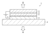
図1に示す発光素子(エレクトロルミネッセンス素子)1は、基板2と、基板2上に形
成された陰極(第一の電極)3と、陰極3に対向する陽極(第二の電極)5とを有する。
発光素子1は、また、陰極3と陽極5との間(一対の電極間)に有機化合物層4が介挿さ
れ、さらに、有機化合物層4と陽極5との間に正孔注入性金属化合物層8が設けられ、有
機化合物層4と陰極3との間に電子注入性金属化合物層6が設けられ、さらに、有機化合
物層4と電子注入性金属化合物層6との間に、製膜後一定時間大気に放置することにより
作製される正孔ブロック性金属化合物層7が設けられている。
A light-emitting element (electroluminescence element) 1 shown in FIG. 1 includes a
In the
ここに封止構造は原理的には必要としない。しかしながら、電極の絶縁性を維持するな
どの意味合いから封止構造を用いても何ら支障はない。
Here, the sealing structure is not necessary in principle. However, there is no problem even if the sealing structure is used from the viewpoint of maintaining the insulating properties of the electrodes.
基板2は、発光素子1の支持体となるものであり、さらにここでは陰極3が直接作製さ
れる支持体でもある。発光素子1は、光の取り出し方向を制限されるものではなく、基板
2側から光を取り出す構成(ボトムエミッション型)の場合と、基板2とは反対側の陽極
5から光を取り出す構成(トップエミッション型)の場合と、その両方が可能な場合(透
明型)の3つが考えられる。ボトムエミッション型の場合、基板2および陰極3は、それ
ぞれ、実質的に透明(無色透明、着色透明または半透明)であり、トップエミッション型
の場合、陽極5が透明であり、透明型の場合、基板2、陰極3、及び陽極5が透明である
。
The
基板2の構成材料としては、例えば、ポリエチレンテレフタレート、ポリエチレンナフ
タレート、ポリプロピレン、シクロオレフィンポリマー、ポリアミド、ポリエーテルサル
フォン、ポリメチルメタクリレート、ポリカーボネート、ポリアリレートのような樹脂材
料や、石英ガラス、ソーダガラスのようなガラス材料等が挙げられ、これらのうちの1種
または2種以上を組み合わせて用いることができる。
Examples of the constituent material of the
このような基板2の平均厚さは、特に限定されないが、0.1〜30mm程度であるの
が好ましく、0.1〜10mm程度であるのがより好ましい。
Although the average thickness of such a board |
なお、トップエミッション型の場合、基板2には、透明基板および不透明基板のいずれ
も用いることができる。
In the case of the top emission type, the
不透明基板としては、例えば、アルミナのようなセラミックス材料で構成された基板、
ステンレス鋼のような金属基板の表面に酸化膜(絶縁膜)を形成したもの、樹脂材料で構
成された基板等が挙げられる。
As an opaque substrate, for example, a substrate made of a ceramic material such as alumina,
Examples include a substrate formed of an oxide film (insulating film) on the surface of a metal substrate such as stainless steel, a substrate made of a resin material, and the like.
本構造における陰極3は、通常の有機EL素子と異なり仕事関数を小さくするという制
約を受けない。つまり、仕事関数の大きな材料を用いることができ、大気下での安定性を
獲得するためにはその方が望ましい。その他に求められる特性としては、導電性に優れて
いること、そしてボトムエミッション型および透明型の場合、その透過性に優れているこ
とである。これらは陽極5においても同様であり、仕事関数が大きく、導電性に優れ、ト
ップエミッション型および透明型の場合、透過性に優れている材料を用いることが望まし
い。
Unlike the normal organic EL element, the
陰極3および陽極5の構成材料としては、例えば、ITO(インジウム酸化錫)、IZ
O(インジウム酸化亜鉛)、FTO(フッ素酸化錫)、In2O3、SnO2、Sb含有S
nO2、Al含有ZnO等の酸化物、Au、Pt、Ag、Cuまたはこれらを含む合金等
が挙げられ、これらのうちの1種または2種以上を組み合わせて用いることができる。
The constituent materials of the
O (indium zinc oxide), FTO (fluorine tin oxide), In 2 O 3 , SnO 2 , Sb-containing S
Examples thereof include oxides such as nO 2 and Al-containing ZnO, Au, Pt, Ag, Cu, and alloys containing these, and one or more of these can be used in combination.
このような陰極3の平均厚さは、特に限定されないが、10〜200nm程度であるの
が好ましく、30〜150nm程度であるのがより好ましい。また、Au、Pt、Ag、
Cu等の不透過な材料を用いる場合でも、例えば平均厚さを10〜30nm程度にするこ
とで、ボトムエミッション型および透明型の陰極として使用することができる。
The average thickness of the
Even when an opaque material such as Cu is used, for example, by setting the average thickness to about 10 to 30 nm, it can be used as a bottom emission type and a transparent type cathode.
一方、陽極5の平均厚さは、特に限定されないが、10〜10000nm程度であるの
が好ましく、30〜50nm程度であるのがより好ましい。また、Au、Pt、Ag、C
u等の不透過な材料を用いる場合でも、例えば平均厚さを10〜30nm程度にすること
で、トップエミッション型および透明型の陽極として使用することができる。
On the other hand, the average thickness of the
Even when an impermeable material such as u is used, it can be used as a top emission type or transparent type anode by setting the average thickness to about 10 to 30 nm, for example.
有機化合物層4は、発光を担う層であり、少なくとも発光材料を含む層である。それゆ
え、発光材料と正孔輸送性有機材料との混合もしくは積層でも構わない。発光材料の構成
材料としては、各種高分子の発光材料(高分子材料)、各種低分子の発光材料(低分子材
料)を単独または組み合わせて用いることができる。特に、ベンゾチアヂアゾール骨格(
以下、「BTユニット」と称する。)を有する有機材料が少なくとも1種類含まれている
ことがより好適である。BTユニットを用いないことも可能である。その場合は後述する
高分子材料、低分子材料をそれぞれ単独、混合して用いることができる。BTユニットを
有する有機材料には、ポリ(ジオクチルフルオレン−アルト−ベンゾチアジアゾール)(
F8BT)、ポリ(N-ドデシル-2,5,-ビス(2’-チエニル)ピロール-2,1,3-ベ
ンゾチアヂアゾール)(PTPTB 文献:C.J.Brabec et.al., Adv.Func.Mater. 12,70
9,(2002) を参照)、4,7−ジフェニル−ベンゾ[1,2,5]チアヂアゾール (F1)、4
,7−ビス−ビェニル−4−イル−ベンゾ[1,2,5]チアヂアゾール (F2)、4,7−
ジ(4−メトキシ−フェニル)−ベンゾ[1,2,5]チアヂアゾール (F3)、4,7−ビス
−(6−メトキシ−ナフタレン−2−イル)−ベンゾ[1,2,5] チアヂアゾール (F4)、
4,7−ジ(2,3−ジヒドロ−チエノ[3,4−b][1,4]ジオキシン−5−イル)−ベ
ンゾ[1,2,5]チアヂアゾール (F5)、4,7−ジ(4−(N,N−ジメチルアミノ)−フェ
ニル)−ベンゾ[1,2,5]チアヂアゾール (F6) (F1からF6 文献:Dmitry Aldakov e
t.al., Chem. Mater. 2005, 17, 5238-5241を参照)、4,7−ビス[5−(4’−トリ
フルオロメチルフェニル)チオフェン−2−イル]ベンゾ[1,2,5]チアヂアゾール (1)
((1) 文献:Takahiro Kono et.al.,Chem. Mater. 2007,19,1218-1220を参照)
、4,7−ビス(4−ジメチルアミノフェニル)−2,1,3−ベンゾチアヂアゾール(2)
、4−(4−ジメチルアミノフェニル)−7−(4−ジフェニルアミノフェニル)−2,1,
3−ベンゾチアヂアゾール(3)、4,7−ビス(4−ジフェニルアミノフェニル)−2,1
,3−ベンゾチアヂアゾール(4)、4,7−ビス{4−[N−(1−ナフチル)−N−フェニル
アミノ]フェニル}−2,1,3−ベンゾチアヂアゾール(5)、4,7−ビス{4−[N−(2
−ナフチル)−N−フェニルアミノ]フェニル}−2,1,3−ベンゾチアヂアゾール(6)、
4,7−ビス(4’−ジフェニルアミノフェニル−4−イル)−2,1,3−ベンゾチアヂ
アゾール(7)、4,7−ビス{5−[4−(ジフェニルアミノ)フェニル]−2−チエニル}−
2,1,3−ベンゾチアヂアゾール(8)、4,7−ビス{2−[4−(ジフェニルアミノ)フ
ェニル]エチニル}−2,1,3−ベンゾチアヂアゾール(9)、4,7−ビス{2−[4−(ジ
フェニルアミノ)フェニル]エチニル}−2,1,3−ベンゾチアヂアゾール(10)((2)か
ら(10) 文献:Shin-ichiro Kato et.al., Chem. Commun. ,2004,23422343を参照)
及びその誘導体、そして2,1,3−ベンゾチアヂアゾールが挙げられる。
The
Hereinafter, it is referred to as “BT unit”. It is more preferable that at least one kind of organic material having) is contained. It is also possible not to use the BT unit. In that case, a polymer material and a low-molecular material described later can be used alone or in combination. Organic materials having BT units include poly (dioctylfluorene-alt-benzothiadiazole) (
F8BT), poly (N-dodecyl-2,5, -bis (2′-thienyl) pyrrole-2,1,3-benzothiadiazole) (PPTTB literature: CJBrabec et.al., Adv. Func. Mater. 12,70
9, (2002)), 4,7-diphenyl-benzo [1,2,5] thiadiazole (F1), 4
, 7-Bis-bienyl-4-yl-benzo [1,2,5] thiadiazole (F2), 4,7-
Di (4-methoxy-phenyl) -benzo [1,2,5] thiadiazole (F3), 4,7-bis- (6-methoxy-naphthalen-2-yl) -benzo [1,2,5] thiadiazole ( F4),
4,7-di (2,3-dihydro-thieno [3,4-b] [1,4] dioxin-5-yl) -benzo [1,2,5] thiadiazole (F5), 4,7-di (4- (N, N-dimethylamino) -phenyl) -benzo [1,2,5] thiadiazole (F6) (F1 to F6 Article: Dmitry Aldakov e
t.al., Chem. Mater. 2005, 17, 5238-5241), 4,7-bis [5- (4′-trifluoromethylphenyl) thiophen-2-yl] benzo [1,2,5 Thiadiazole (1)
(See (1) Literature: Takahiro Kono et.al., Chem. Mater. 2007, 19, 1218-1220)
4,7-bis (4-dimethylaminophenyl) -2,1,3-benzothiadiazole (2)
4- (4-dimethylaminophenyl) -7- (4-diphenylaminophenyl) -2,1,
3-benzothiadiazole (3), 4,7-bis (4-diphenylaminophenyl) -2,1
, 3-Benzothiadiazole (4), 4,7-bis {4- [N- (1-naphthyl) -N-phenylamino] phenyl} -2,1,3-benzothiadiazole (5), 4,7-bis {4- [N- (2
-Naphthyl) -N-phenylamino] phenyl} -2,1,3-benzothiadiazole (6),
4,7-bis (4′-diphenylaminophenyl-4-yl) -2,1,3-benzothiadiazole (7), 4,7-bis {5- [4- (diphenylamino) phenyl]- 2-thienyl}-
2,1,3-benzothiadiazole (8), 4,7-bis {2- [4- (diphenylamino) phenyl] ethynyl} -2,1,3-benzothiadiazole (9), 4, 7-bis {2- [4- (diphenylamino) phenyl] ethynyl} -2,1,3-benzothiadiazole (10) ((2) to (10) Article: Shin-ichiro Kato et.al., Chem. Commun., 2004, 23422343)
And its derivatives, and 2,1,3-benzothiadiazole.
BTユニットを用いる場合、他の有機材料と混合して用いることができる。具体的には
、電子デバイスとして機能する高分子材料(発光材料、電子輸送性材料、正孔輸送性有機
材料)若しくは低分子(発光材料、電子輸送性材料、正孔輸送性有機材料)等が挙げられ
る。これらに制限されることはない。
When using a BT unit, it can be used by mixing with other organic materials. Specifically, polymer materials (light-emitting materials, electron-transport materials, hole-transport organic materials) or small molecules (light-emitting materials, electron-transport materials, hole-transport organic materials) that function as electronic devices are used. Can be mentioned. It is not limited to these.
高分子の発光材料若しくは電子輸送性材料としては、例えば、トランス型ポリアセチレ
ン、シス型ポリアセチレン、ポリ(ジ−フェニルアセチレン)(PDPA)、ポリ(アル
キル,フェニルアセチレン)(PAPA)のようなポリアセチレン系化合物、ポリ(パラ
−フェンビニレン)(PPV)、ポリ(2,5−ジアルコキシ−パラ−フェニレンビニレ
ン)(RO−PPV)、シアノ−置換−ポリ(パラ−フェンビニレン)(CN−PPV)
、ポリ(2−ジメチルオクチルシリル−パラ−フェニレンビニレン)(DMOS−PPV
)、ポリ(2−メトキシ,5−(2’−エチルヘキソキシ)−パラ−フェニレンビニレン
)(MEH−PPV)のようなポリパラフェニレンビニレン系化合物、ポリ(3−アルキ
ルチオフェン)(PAT)、ポリ(オキシプロピレン)トリオール(POPT)のような
ポリチオフェン系化合物、ポリ(9,9−ジアルキルフルオレン)(PDAF)、ポリ(
ジオクチルフルオレン−アルト−ベンゾチアジアゾール)(F8BT)、α,ω−ビス[
N,N’−ジ(メチルフェニル)アミノフェニル]−ポリ[9,9−ビス(2−エチルヘ
キシル)フルオレン−2,7−ジル](PF2/6am4)、ポリ(9,9−ジオクチル
−2,7−ジビニレンフルオレニル−オルト−コ(アントラセン−9,10−ジイル)の
ようなポリフルオレン系化合物、ポリ(パラ−フェニレン)(PPP)、ポリ(1,5−
ジアルコキシ−パラ−フェニレン)(RO−PPP)のようなポリパラフェニレン系化合
物、ポリ(N−ビニルカルバゾール)(PVK)のようなポリカルバゾール系化合物、ポ
リ(メチルフェニルシラン)(PMPS)、ポリ(ナフチルフェニルシラン)(PNPS
)、ポリ(ビフェニリルフェニルシラン)(PBPS)のようなポリシラン系化合物等が
挙げられる。
Examples of the polymer light-emitting material or electron-transporting material include polyacetylene-based compounds such as trans-type polyacetylene, cis-type polyacetylene, poly (di-phenylacetylene) (PDPA), and poly (alkyl, phenylacetylene) (PAPA). , Poly (para-phenvinylene) (PPV), poly (2,5-dialkoxy-para-phenylenevinylene) (RO-PPV), cyano-substituted-poly (para-phenvinylene) (CN-PPV)
, Poly (2-dimethyloctylsilyl-para-phenylenevinylene) (DMOS-PPV
), Poly (2-methoxy, 5- (2′-ethylhexoxy) -para-phenylenevinylene) (MEH-PPV), polyparaphenylenevinylene compounds such as poly (3-alkylthiophene) (PAT), poly ( Polythiophene compounds such as oxypropylene) triol (POPT), poly (9,9-dialkylfluorene) (PDAF), poly (
Dioctylfluorene-alt-benzothiadiazole) (F8BT), α, ω-bis [
N, N'-di (methylphenyl) aminophenyl] -poly [9,9-bis (2-ethylhexyl) fluorene-2,7-zyl] (PF2 / 6am4), poly (9,9-dioctyl-2, Polyfluorene compounds such as 7-divinylenefluorenyl-ortho-co (anthracene-9,10-diyl), poly (para-phenylene) (PPP), poly (1,5-
Polyparaphenylene compounds such as dialkoxy-para-phenylene) (RO-PPP), polycarbazole compounds such as poly (N-vinylcarbazole) (PVK), poly (methylphenylsilane) (PMPS), poly (Naphthylphenylsilane) (PNPS
) And polysilane compounds such as poly (biphenylylphenylsilane) (PBPS).
一方、低分子の発光材料若しくは電子輸送性材料としては、例えば、配位子に2,2’
−ビピリジン−4,4’−ジカルボン酸を持つ、3配位のイリジウム錯体、ファクトリス
(2−フェニルピリジン)イリジウム(Ir(ppy)3)、8−ヒドロキシキノリン
アルミニウム(Alq3)、トリス(4−メチル−8キノリノレート)アルミニウム(III
)(Almq3)、8−ヒドロキシキノリン亜鉛(Znq2)、(1,10−フェナントロ
リン)−トリス−(4,4,4−トリフルオロ−1−(2−チエニル)−ブタン−1,3
−ジオネート)ユーロピウム(III)(Eu(TTA)3(phen))、2,3,7,8
,12,13,17,18−オクタエチル−21H,23H−ポルフィン プラチナム(
II)のような各種金属錯体、ジスチリルベンゼン(DSB)、ジアミノジスチリルベンゼ
ン(DADSB)のようなベンゼン系化合物、ナフタレン、ナイルレッドのようなナフタ
レン系化合物、フェナントレンのようなフェナントレン系化合物、クリセン、6−ニトロ
クリセンのようなクリセン系化合物、ペリレン、N,N’−ビス(2,5−ジ−t−ブチ
ルフェニル)−3,4,9,10−ペリレン−ジ−カルボキシイミド(BPPC)のよう
なペリレン系化合物、コロネンのようなコロネン系化合物、アントラセン、ビススチリル
アントラセンのようなアントラセン系化合物、ピレンのようなピレン系化合物、4−(ジ
−シアノメチレン)−2−メチル−6−(パラ−ジメチルアミノスチリル)−4H−ピラ
ン(DCM)のようなピラン系化合物、アクリジンのようなアクリジン系化合物、スチル
ベンのようなスチルベン系化合物、2,5−ジベンゾオキサゾールチオフェンのようなチ
オフェン系化合物、ベンゾオキサゾールのようなベンゾオキサゾール系化合物、ベンゾイ
ミダゾールのようなベンゾイミダゾール系化合物、2,2’−(パラ−フェニレンジビニ
レン)−ビスベンゾチアゾールのようなベンゾチアゾール系化合物、ビスチリル(1,4
−ジフェニル−1,3−ブタジエン)、テトラフェニルブタジエンのようなブタジエン系
化合物、ナフタルイミドのようなナフタルイミド系化合物、クマリンのようなクマリン系
化合物、ペリノンのようなペリノン系化合物、オキサジアゾールのようなオキサジアゾー
ル系化合物、アルダジン系化合物、1,2,3,4,5−ペンタフェニル−1,3−シク
ロペンタジエン(PPCP)のようなシクロペンタジエン系化合物、キナクリドン、キナ
クリドンレッドのようなキナクリドン系化合物、ピロロピリジン、チアジアゾロピリジン
のようなピリジン系化合物、2,2’,7,7’−テトラフェニル−9,9’−スピロビ
フルオレンのようなスピロ化合物、フタロシアニン(H2Pc)、銅フタロシアニンのよ
うな金属または無金属のフタロシアニン系化合物等が挙げられる。
On the other hand, as a low-molecular light-emitting material or electron-transporting material, for example, 2, 2 ′ is used as a ligand.
-Tricoordinate iridium complexes with bipyridine-4,4'-dicarboxylic acid, factory (2-phenylpyridine) iridium (Ir (ppy) 3), 8-hydroxyquinoline
Aluminum (Alq3), Tris (4-methyl-8quinolinolate) Aluminum (III
) (Almq3), 8-hydroxyquinoline zinc (Znq2), (1,10-phenanthroline) -tris- (4,4,4-trifluoro-1- (2-thienyl) -butane-1,3
-Dionate) Europium (III) (Eu (TTA) 3 (phen)), 2, 3, 7, 8
, 12, 13, 17, 18-octaethyl-21H, 23H-porphine platinum (
II) various metal complexes, distyrylbenzene (DSB), benzene compounds such as diamino distyrylbenzene (DADSB), naphthalene compounds such as naphthalene and nile red, phenanthrene compounds such as phenanthrene, chrysene , Chrysene compounds such as 6-nitrochrysene, perylene, N, N′-bis (2,5-di-t-butylphenyl) -3,4,9,10-perylene-di-carboximide (BPPC) Perylene compounds such as coronene, coronene compounds such as coronene, anthracene compounds such as anthracene and bisstyrylanthracene, pyrene compounds such as pyrene, 4- (di-cyanomethylene) -2-methyl-6 A pyran system such as (para-dimethylaminostyryl) -4H-pyran (DCM) Compound, acridine compound such as acridine, stilbene compound such as stilbene, thiophene compound such as 2,5-dibenzoxazole thiophene, benzoxazole compound such as benzoxazole, benzimidazole such as benzimidazole Compounds, benzothiazole compounds such as 2,2 ′-(para-phenylenedivinylene) -bisbenzothiazole, bistyryl (1,4
-Diphenyl-1,3-butadiene), butadiene compounds such as tetraphenylbutadiene, naphthalimide compounds such as naphthalimide, coumarin compounds such as coumarin, perinone compounds such as perinone, oxadiazole Oxadiazole compounds, aldazine compounds, cyclopentadiene compounds such as 1,2,3,4,5-pentaphenyl-1,3-cyclopentadiene (PPCP), quinacridones such as quinacridone and quinacridone red Compounds, pyridine compounds such as pyrrolopyridine and thiadiazolopyridine, spiro compounds such as 2,2 ′, 7,7′-tetraphenyl-9,9′-spirobifluorene, phthalocyanine (H 2 Pc) Metallic or non-metallic phthalos such as copper phthalocyanine Nin-based compounds, and the like.
高分子の正孔輸送性有機材料としては、例えば、ポリアリールアミン、フルオレン−ア
リールアミン共重合体、フルオレン−ビチオフェン共重合体、ポリ(N−ビニルカルバゾ
ール)、ポリビニルピレン、ポリビニルアントラセン、ポリチオフェン、ポリアルキルチ
オフェン、ポリヘキシルチオフェン、ポリ(p−フェニレンビニレン)、ポリチニレンビ
ニレン、ピレンホルムアルデヒド樹脂、エチルカルバゾールホルムアルデヒド樹脂または
その誘導体等が挙げられる。
Examples of the polymer hole transporting organic material include polyarylamine, fluorene-arylamine copolymer, fluorene-bithiophene copolymer, poly (N-vinylcarbazole), polyvinylpyrene, polyvinylanthracene, polythiophene, polythiophene. Examples thereof include alkylthiophene, polyhexylthiophene, poly (p-phenylene vinylene), polytinylene vinylene, pyrene formaldehyde resin, ethyl carbazole formaldehyde resin or derivatives thereof.
また、上記化合物は、他の化合物との混合物として用いることもできる。一例として、
ポリチオフェンを含有する混合物としては、ポリ(3,4−エチレンジオキシチオフェン
/スチレンスルホン酸)(PEDOT/PSS)等が挙げられる。
Moreover, the said compound can also be used as a mixture with another compound. As an example,
Examples of the mixture containing polythiophene include poly (3,4-ethylenedioxythiophene / styrene sulfonic acid) (PEDOT / PSS).
一方、低分子材料の正孔輸送性有機材料としては、例えば、1,1−ビス(4−ジ−パ
ラ−トリアミノフェニル)シクロへキサン、1,1’−ビス(4−ジ−パラ−トリルアミ
ノフェニル)−4−フェニル−シクロヘキサンのようなアリールシクロアルカン系化合物
、4,4’,4’’−トリメチルトリフェニルアミン、N,N,N’,N’−テトラフェ
ニル−1,1’−ビフェニル−4,4’−ジアミン、N,N’−ジフェニル−N,N’−
ビス(3−メチルフェニル)−1,1’−ビフェニル−4,4’−ジアミン(TPD1)
、N,N’−ジフェニル−N,N’−ビス(4−メトキシフェニル)−1,1’−ビフェ
ニル−4,4’−ジアミン(TPD2)、N,N,N’,N’−テトラキス(4−メトキ
シフェニル)−1,1’−ビフェニル−4,4’−ジアミン(TPD3)、N,N’−ジ
(1−ナフチル)−N,N’−ジフェニル−1,1’−ビフェニル−4,4’−ジアミン
(α−NPD)のようなジアミン系化合物、N,N,N’,N’−テトラフェニル−パラ
−フェニレンジアミン、N,N,N’,N’−テトラ(パラ−トリル)−パラ−フェニレ
ンジアミン、N,N,N’,N’−テトラ(メタ−トリル)−メタ−フェニレンジアミン
(PDA)のようなフェニレンジアミン系化合物、カルバゾール、N−イソプロピルカル
バゾール、N−フェニルカルバゾールのようなカルバゾール系化合物、スチルベン、4−
ジ−パラ−トリルアミノスチルベンのようなスチルベン系化合物、OxZのようなオキサ
ゾール系化合物、トリフェニルメタン、m−MTDATAのようなトリフェニルメタン系
化合物、1−フェニル−3−(パラ−ジメチルアミノフェニル)ピラゾリンのようなピラ
ゾリン系化合物、ベンジン(シクロヘキサジエン)系化合物、トリアゾールのようなトリ
アゾール系化合物、イミダゾールのようなイミダゾール系化合物、1,3,4−オキサジ
アゾール、2,5−ジ(4−ジメチルアミノフェニル)−1,3,4,−オキサジアゾー
ルのようなオキサジアゾール系化合物、アントラセン、9−(4−ジエチルアミノスチリ
ル)アントラセンのようなアントラセン系化合物、フルオレノン、2,4,7,−トリニ
トロ−9−フルオレノン、2,7−ビス(2−ヒドロキシ−3−(2−クロロフェニルカ
ルバモイル)−1−ナフチルアゾ)フルオレノンのようなフルオレノン系化合物、ポリア
ニリンのようなアニリン系化合物、シラン系化合物、1,4−ジチオケト−3,6−ジフ
ェニル−ピロロ−(3,4−c)ピロロピロールのようなピロール系化合物、フローレン
のようなフローレン系化合物、ポルフィリン、金属テトラフェニルポルフィリンのような
ポルフィリン系化合物、キナクリドンのようなキナクリドン系化合物、フタロシアニン、
銅フタロシアニン、テトラ(t−ブチル)銅フタロシアニン、鉄フタロシアニンのような
金属または無金属のフタロシアニン系化合物、銅ナフタロシアニン、バナジルナフタロシ
アニン、モノクロロガリウムナフタロシアニンのような金属または無金属のナフタロシア
ニン系化合物、N,N’−ジ(ナフタレン−1−イル)−N,N’−ジフェニル−ベンジ
ジン、N,N,N’,N’−テトラフェニルベンジジンのようなベンジジン系化合物等が
挙げられる。
On the other hand, examples of the low molecular weight hole transporting organic material include 1,1-bis (4-di-para-triaminophenyl) cyclohexane and 1,1′-bis (4-di-para-). Arylcycloalkane compounds such as (tolylaminophenyl) -4-phenyl-cyclohexane, 4,4 ′, 4 ″ -trimethyltriphenylamine, N, N, N ′, N′-tetraphenyl-1,1 ′ -Biphenyl-4,4'-diamine, N, N'-diphenyl-N, N'-
Bis (3-methylphenyl) -1,1′-biphenyl-4,4′-diamine (TPD1)
N, N′-diphenyl-N, N′-bis (4-methoxyphenyl) -1,1′-biphenyl-4,4′-diamine (TPD2), N, N, N ′, N′-tetrakis ( 4-methoxyphenyl) -1,1′-biphenyl-4,4′-diamine (TPD3), N, N′-di (1-naphthyl) -N, N′-diphenyl-1,1′-biphenyl-4 , 4′-diamine (α-NPD), N, N, N ′, N′-tetraphenyl-para-phenylenediamine, N, N, N ′, N′-tetra (para-tolyl) ) -Para-phenylenediamine, phenylenediamine compounds such as N, N, N ′, N′-tetra (meta-tolyl) -meta-phenylenediamine (PDA), carbazole, N-isopropylcarbazole, N-phenylcarbazole Carbazo like Le compounds, stilbene, 4-
Stilbene compounds such as di-para-tolylaminostilbene, oxazole compounds such as OxZ, triphenylmethane, triphenylmethane compounds such as m-MTDATA, 1-phenyl-3- (para-dimethylaminophenyl) ) Pyrazoline compounds such as pyrazoline, benzine (cyclohexadiene) compounds, triazole compounds such as triazole, imidazole compounds such as imidazole, 1,3,4-oxadiazole, 2,5-di (4 -Dimethylaminophenyl) -1,3,4, -oxadiazole compounds such as oxadiazole, anthracene, anthracene compounds such as 9- (4-diethylaminostyryl) anthracene, fluorenone, 2,4,7 , -Trinitro-9-fluorenone, 2, Fluorenone compounds such as 7-bis (2-hydroxy-3- (2-chlorophenylcarbamoyl) -1-naphthylazo) fluorenone, aniline compounds such as polyaniline, silane compounds, 1,4-dithioketo-3,6 A pyrrole compound such as diphenyl-pyrrolo- (3,4-c) pyrrolopyrrole, a fluorene compound such as florene, a porphyrin, a porphyrin compound such as metal tetraphenylporphyrin, a quinacridone compound such as quinacridone, Phthalocyanine,
Metallic or metal-free phthalocyanine compounds such as copper phthalocyanine, tetra (t-butyl) copper phthalocyanine, iron phthalocyanine, copper or metal-free naphthalocyanine compounds such as copper naphthalocyanine, vanadyl naphthalocyanine, monochlorogallium naphthalocyanine And benzidine compounds such as N, N′-di (naphthalen-1-yl) -N, N′-diphenyl-benzidine and N, N, N ′, N′-tetraphenylbenzidine.
この有機化合物層4の形成には、高分子材料を含む場合には、例えば、スピンコート法
、キャスティング法、マイクログラビアコート法、グラビアコート法、バーコート法、ロ
ールコート法、ワイヤーバーコート法、ディップコート法、スプレーコート法、スクリー
ン印刷法、フレキソ印刷法、オフセット印刷法、インクジェット印刷法等の各種塗布法を
用いることができる。スピンコート法等の場合は基板上全面に塗布した後、フォトリソグ
ラフィー等でパターニングを行う。また、インクジェット印刷法等では、周囲を隔壁で囲
まれた領域に滴下することで、所定の領域にのみ成膜できる。
For the formation of the
この場合に用いられる溶媒には、例えば、硝酸、硫酸、アンモニア、過酸化水素、水、
二硫化炭素、四塩化炭素、エチレンカーボネイト等の無機溶媒や、メチルエチルケトン(
MEK)、アセトン、ジエチルケトン、メチルイソブチルケトン(MIBK)、メチルイ
ソプロピルケトン(MIPK)、シクロヘキサノン等のケトン系溶媒、メタノール、エタ
ノール、イソプロパノール、エチレングリコール、ジエチレングリコール(DEG)、グ
リセリン等のアルコール系溶媒、ジエチルエーテル、ジイソプロピルエーテル、1,2−
ジメトキシエタン(DME)、1,4−ジオキサン、テトラヒドロフラン(THF)、テ
トラヒドロピラン(THP)、アニソール、ジエチレングリコールジメチルエーテル(ジ
グリム)、ジエチレングリコールエチルエーテル(カルビトール)等のエーテル系溶媒、
メチルセロソルブ、エチルセロソルブ、フェニルセロソルブ等のセロソルブ系溶媒、ヘキ
サン、ペンタン、ヘプタン、シクロヘキサン等の脂肪族炭化水素系溶媒、トルエン、キシ
レン、ベンゼン等の芳香族炭化水素系溶媒、ピリジン、ピラジン、フラン、ピロール、チ
オフェン、メチルピロリドン等の芳香族複素環化合物系溶媒、N,N−ジメチルホルムア
ミド(DMF)、N,N−ジメチルアセトアミド(DMA)等のアミド系溶媒、クロロベ
ンゼン、ジクロロメタン、クロロホルム、1,2−ジクロロエタン等のハロゲン化合物系
溶媒、酢酸エチル、酢酸メチル、ギ酸エチル等のエステル系溶媒、ジメチルスルホキシド
(DMSO)、スルホラン等の硫黄化合物系溶媒、アセトニトリル、プロピオニトリル、
アクリロニトリル等のニトリル系溶媒、ギ酸、酢酸、トリクロロ酢酸、トリフルオロ酢酸
等の有機酸系溶媒のような各種有機溶媒、または、これらを含む混合溶媒等が挙げられる
。
Examples of the solvent used in this case include nitric acid, sulfuric acid, ammonia, hydrogen peroxide, water,
Inorganic solvents such as carbon disulfide, carbon tetrachloride, ethylene carbonate, methyl ethyl ketone (
MEK), ketone solvents such as acetone, diethyl ketone, methyl isobutyl ketone (MIBK), methyl isopropyl ketone (MIPK), cyclohexanone, alcohol solvents such as methanol, ethanol, isopropanol, ethylene glycol, diethylene glycol (DEG), glycerin, Diethyl ether, diisopropyl ether, 1,2-
Ether solvents such as dimethoxyethane (DME), 1,4-dioxane, tetrahydrofuran (THF), tetrahydropyran (THP), anisole, diethylene glycol dimethyl ether (diglyme), diethylene glycol ethyl ether (carbitol),
Cellosolve solvents such as methyl cellosolve, ethyl cellosolve, phenyl cellosolve, aliphatic hydrocarbon solvents such as hexane, pentane, heptane, cyclohexane, aromatic hydrocarbon solvents such as toluene, xylene, benzene, pyridine, pyrazine, furan, Aromatic heterocyclic compounds such as pyrrole, thiophene and methylpyrrolidone, amides such as N, N-dimethylformamide (DMF) and N, N-dimethylacetamide (DMA), chlorobenzene, dichloromethane, chloroform, 1,2 -Halogen compound solvents such as dichloroethane, ester solvents such as ethyl acetate, methyl acetate, ethyl formate, sulfur compound solvents such as dimethyl sulfoxide (DMSO), sulfolane, acetonitrile, propionitrile,
Examples thereof include nitrile solvents such as acrylonitrile, various organic solvents such as organic acid solvents such as formic acid, acetic acid, trichloroacetic acid and trifluoroacetic acid, or mixed solvents containing these.
これらの中でも、溶媒としては、非極性溶媒が好適であり、例えば、キシレン、トルエ
ン、シクロヘキシルベンゼン、ジハイドロベンゾフラン、トリメチルベンゼン、テトラメ
チルベンゼン等の芳香族炭化水素系溶媒、ピリジン、ピラジン、フラン、ピロール、チオ
フェン、メチルピロリドン等の芳香族複素環化合物系溶媒、ヘキサン、ペンタン、ヘプタ
ン、シクロヘキサン等の脂肪族炭化水素系溶媒等が挙げられ、これらを単独または混合し
て用いることができる。
Among these, as the solvent, a nonpolar solvent is suitable, for example, an aromatic hydrocarbon solvent such as xylene, toluene, cyclohexylbenzene, dihydrobenzofuran, trimethylbenzene, tetramethylbenzene, pyridine, pyrazine, furan, Examples include aromatic heterocyclic compound solvents such as pyrrole, thiophene, and methylpyrrolidone, and aliphatic hydrocarbon solvents such as hexane, pentane, heptane, and cyclohexane. These can be used alone or in combination.
なお、分解せず成膜が可能ならば、高分子材料を含む材料であっても、以下の気相成膜
法を用いることもできる。
Note that the following vapor phase film formation method can be used even if the material includes a polymer material as long as the film can be formed without being decomposed.
低分子材料の場合には、真空蒸着法等の気相成膜法を用いることができる。混合物の場
合は共蒸着等の気相成膜法を用いる。塗布法により、結晶化等せずに良好な薄膜が形成さ
れるときは、上記塗布法も用いることができる。有機化合物層4の膜厚は特に限定されな
いが、電子デバイスの種類により、最適な値にすることができる。
In the case of a low molecular material, a vapor phase film forming method such as a vacuum evaporation method can be used. In the case of a mixture, a vapor deposition method such as co-evaporation is used. When a good thin film is formed without crystallization or the like by the coating method, the above coating method can also be used. The film thickness of the
このような有機化合物層4の平均厚さは、特に限定されないが、10〜150nm程度
であるのが好ましく、40〜100nm程度であるのがより好ましい。
The average thickness of the
有機化合物層4は、正孔注入性金属化合物層8から注入された正孔を輸送するとともに
、電子注入性金属化合物層6から製膜後一定時間大気に放置することにより作製される正
孔ブロック性金属化合物層7を経由して電子を受け取る。そして正孔と電子とが再結合し
、この再結合に際して放出されたエネルギーによりエキシトン(励起子)が生成し、エキ
シトンが基底状態に戻る際にエネルギー(蛍光やりん光)を放出(発光)する。この時、
より高効率に正孔と電子とを再結合させ、電子注入性金属化合物層6上での有機化合物層
4の化学的劣化を防ぐことを目的とし、正孔ブロック性金属化合物層7は配置される。
The
The hole blocking
これらの中でも、有機化合物層4の構成材料としては、高分子の発光材料を主とするも
のが好ましい。液相プロセスにより製膜が可能な高分子材料は、高価な装置を必要とせず
、より低エネルギーで作製できる。
Among these, as a constituent material of the
電子注入性金属化合物層6は陰極3より電子を注入し有機化合物層4へと輸送する。こ
のような電子注入性金属化合物層6を構成する金属酸化物としては、伝導バンドのエネル
ギー準位が高いものが好ましく、特に限定されないが、酸化チタン(TiO2)、酸化亜
鉛(ZnO)、酸化タングステン(WO3)、酸化二オブ(Nb2O5)、酸化鉄(Fe2O
3)等があげられ、これらのうち1種または2種以上を組み合わせ用いることができる。
The electron injecting
3 ) and the like, and one or more of these can be used in combination.
この電子注入性金属化合物層6の成膜方法については、特に制限されるものではなく、
気相成膜法であるプラズマCVD、熱CVD、レーザーCVD等の化学蒸着法(CVD)
、真空蒸着、スパッタリング、イオンプレーティング等の乾式メッキ法、溶射法、そして
液相成膜法である電解メッキ、浸漬メッキ、無電解メッキ等の湿式メッキ法、ゾル・ゲル
法、MOD法、スプレイ熱分解法、微粒子分散液を用いたドクターブレイド法、スピンコ
ート法、インクジェット法、スクリーンプリンティング法などの印刷技術を用いることが
できる。本構造では、スプレイ熱分解法を用いた。
The film forming method of the electron injecting
Chemical vapor deposition (CVD) such as plasma CVD, thermal CVD, laser CVD, etc.
, Vacuum plating, sputtering, ion plating and other dry plating methods, thermal spraying, and liquid phase film forming methods such as electrolytic plating, immersion plating, electroless plating, and other wet plating methods, sol-gel method, MOD method, spraying Printing techniques such as a thermal decomposition method, a doctor blade method using a fine particle dispersion, a spin coating method, an ink jet method, and a screen printing method can be used. In this structure, the spray pyrolysis method was used.
このような電子注入性金属化合物層6の平均厚さは、特に限定されないが、1〜100
0nm程度であるのが好ましく、20〜200nm程度であるのがより好ましい。
The average thickness of the electron injecting
The thickness is preferably about 0 nm, and more preferably about 20 to 200 nm.
正孔ブロック性金属化合物層7は、陽極5より正孔注入性金属化合物層8を経由して有
機化合物層4に注入された大量の正孔をブロックし、有機化合物層4で効率よく電子と再
結合させるものである。この正孔ブロック性金属化合物層7には、大気下で安定に存在す
る絶縁性の薄膜が好ましい。
The hole blocking
このような正孔ブロック性金属化合物層7を構成する金属化合物としては、エネルギー
ギャップの広いものが好ましく、特に限定されないが、酸化セシウム(Cs2O)、酸化カル
シウム(CaO)などアルカリ金属およびアルカリ土類金属の酸化物やその他の金属酸化物
が挙げられ、これらのうち1種または2種以上を組み合わせ用いることができる。
The metal compound constituting the hole blocking
ここでは、大気下での高安定性が第一条件であるため、大気下で平衡状態近くまで放置
することでその材料を作製した。その時間は、15分以上24時間未満である。さらに、
ここでは、より安価に安全に所望の薄膜を作製するために炭酸化合物を用いた。炭酸化合
物は、製膜時もしくは製膜後大気下で金属酸化物に変化する。さらに金属によっては金属
水酸化物まで変化する。その程度は、放置する環境に依存する。つまり、素子を大気下で
放置して、劣化していく過程を素子作製中にすでに取り入れていることになる。これによ
り、素子化後の水分および酸素による化学変化がもたらす空隙などの界面の変化を回避も
しくは軽減でき、素子の長寿命化につながると考えられる。膜厚は、正孔をブロックし、
かつ電子を注入する機能が必要なため、1〜50nmが好適であり、特に5〜30nmが
より好適である。
Here, since the high stability under the atmosphere is the first condition, the material was produced by leaving it to near the equilibrium state under the atmosphere. The time is 15 minutes or more and less than 24 hours. further,
Here, a carbonic acid compound was used in order to produce a desired thin film more inexpensively and safely. The carbonic acid compound changes to a metal oxide during film formation or in the air after film formation. Furthermore, depending on the metal, it changes to a metal hydroxide. The degree depends on the environment to be left unattended. In other words, the process of leaving the element in the atmosphere and deteriorating has already been taken in during the preparation of the element. Thereby, it is considered that changes in the interface such as voids caused by chemical changes due to moisture and oxygen after the device can be avoided or reduced, leading to a longer lifetime of the device. The film thickness blocks holes,
In addition, since a function for injecting electrons is required, 1 to 50 nm is preferable, and 5 to 30 nm is particularly preferable.
このような正孔ブロック性金属化合物層7の成膜方法については、特に制限されるもの
ではなく、気相成膜法であるプラズマCVD、熱CVD、レーザーCVD等の化学蒸着法
(CVD)、真空蒸着、スパッタリング、イオンプレーティング等の乾式メッキ法、溶射
法、そして液相成膜法である電解メッキ、浸漬メッキ、無電解メッキ等の湿式メッキ法、
ゾル・ゲル法、MOD法、スプレイ熱分解法、微粒子分散液を用いたドクターブレイド法
、スピンコート法、インクジェット法、スクリーンプリンティング法などの印刷技術を用
いることができる。本構造では、真空蒸着法を用いた。
The film forming method of the hole blocking
Printing techniques such as a sol-gel method, an MOD method, a spray pyrolysis method, a doctor blade method using a fine particle dispersion, a spin coating method, an ink jet method, and a screen printing method can be used. In this structure, a vacuum deposition method was used.
このような正孔ブロック性金属化合物層7の平均厚さは、特に限定されないが、1〜1
00nm程度であるのが好ましく、5〜20nm程度であるのがより好ましい。
The average thickness of the hole blocking
It is preferably about 00 nm, and more preferably about 5 to 20 nm.
正孔注入性金属化合物層8は陽極5より正孔を注入し有機化合物層4へと輸送する。こ
のような正孔注入性金属化合物層8を構成する金属酸化物としては、仕事関数が大きな化
合物が好ましく、特に限定されないが、例えば、酸化バナジウム(V2O5)、酸化モリブ
テン(MoO3)、酸化ルテニウム(RuO2)等が挙げられ、これらのうちの1種または
2種以上を組み合わせて用いることができる。
The hole injecting
これらの中でも、特に、酸化バナジウムもしくは酸化モリブテンを主成分とするものが
好適である。酸化バナジウムもしくは酸化モリブテンを主材料として構成することにより
、正孔注入性金属化合物層8を前述した能力に特に優れたものとすることができる。
Among these, those containing vanadium oxide or molybdenum oxide as the main component are particularly suitable. By using vanadium oxide or molybdenum oxide as a main material, the hole injecting
この正孔注入性金属化合物層8の成膜方法については、特に制限されるものではなく、
気相成膜法であるプラズマCVD、熱CVD、レーザーCVD等の化学蒸着法(CVD)
、真空蒸着、スパッタリング、イオンプレーティング等の乾式メッキ法、溶射法、そして
液相成膜法である電解メッキ、浸漬メッキ、無電解メッキ等の湿式メッキ法、ゾル・ゲル
法、MOD法、スプレイ熱分解法、微粒子分散液を用いたドクターブレイド法、スピンコ
ート法、インクジェット法、スクリーンプリンティング法などの印刷技術を用いることが
できる。本構造では、真空蒸着法を用いた。
The film forming method of the hole injecting
Chemical vapor deposition (CVD) such as plasma CVD, thermal CVD, laser CVD, etc.
, Vacuum plating, sputtering, ion plating and other dry plating methods, thermal spraying, and liquid phase film forming methods such as electrolytic plating, immersion plating, electroless plating, and other wet plating methods, sol-gel method, MOD method, spraying Printing techniques such as a thermal decomposition method, a doctor blade method using a fine particle dispersion, a spin coating method, an ink jet method, and a screen printing method can be used. In this structure, a vacuum deposition method was used.
このような正孔注入性金属化合物層8の平均厚さは、特に限定されないが、1〜100
0nm程度であるのが好ましく、5〜50nm程度であるのがより好ましい。
The average thickness of the hole injecting
The thickness is preferably about 0 nm, and more preferably about 5 to 50 nm.
本構造では特に必要としないが、封止構造の構成材料としては、一般的に用いられる封
止材料を用いることができる。例えば、Al、Au、Cr、Nb、Ta、Tiまたはこれ
らを含む合金、酸化シリコン、各種樹脂材料等を挙げることができる。
Although not particularly required in this structure, a sealing material generally used can be used as a constituent material of the sealing structure. For example, Al, Au, Cr, Nb, Ta, Ti or alloys containing these, silicon oxide, various resin materials, and the like can be given.
要約すれば、有機化合物層4と陰極3の間、そして有機化合物層4と陽極5の間に、金
属化合物を設け、さらに主たるキャリア、即ち、正孔を有機化合物層4にとどめるために
ブロック層を挿入し、それを大気下で放置することにより作製したことに特徴とする。
In summary, a metal compound is provided between the
有機化合物層4と陰極3の間の電子注入性金属化合物層6は、陰極3自身に大気安定な
仕事関数の大きな材料を用いることを可能にした。通常、電子注入のために仕事関数の小
さい材料を陰極に使用する必要があるところを、その内部の電子注入部に、伝導バンドの
エネルギー準位の高い、既に酸化した金属酸化物を用いることで、大気下での安定な電子
注入を実現したものである。そのため、陰極3と金属酸化物(電子注入性金属化合物層6
)との十分な電気的、物理的接触が必要であり、そのため、一例として基板2側に陰極3
を配する構造をとった。これにより、十分な温度等のプロセスを与えることができる。そ
の観点からは、以下の実施例で示す金属酸化物系導電材料を陰極3とし、その上に例えば
熱分解法などの電極との接触を十分にとれる過程が含まれる工程により作製されることが
より好ましい。もちろんその他の方法でも可能である。
The electron injecting
In this case, sufficient electrical and physical contact with the
The structure was arranged. Thereby, a process such as a sufficient temperature can be provided. From this point of view, the metal oxide-based conductive material shown in the following example is used as the
有機化合物層4と陽極5の間の正孔注入性金属化合物層8は、大気下でより安定な素子
を実現するため、ここでも金属化合物層、特に金属酸化物層を用いた。ここでは、有機化
合物層4と正孔注入性金属酸化物層8との電気的、物理的接触を確実なものにするため、
プロセス上の観点から気相成膜法を用いることがより好ましい。もちろんその他の方法で
も可能である。
As the hole-injecting
From the viewpoint of the process, it is more preferable to use a vapor deposition method. Of course, other methods are possible.
加えて、有機化合物層4と電子注入性金属化合物層6の間に、正孔ブロック性金属化合
物層7として、アルカリ金属もしくはアルカリ土類金属の炭酸化合物薄膜を大気下で放置
することにより、その環境において平衡状態に達した金属化合物薄膜を用いた。ここでは
、上記二つの特徴で達成した大気下での安定かつ効率的な発光をさらに高効率、高安定な
ものにした。具体的には、過剰な正孔が陰極3に抜けることを防ぐと共に、有機化合物層
4/電子注入性金属化合物層6界面で発生しやすい酸化および水分による物理的電気的接
触の不良を改善するものである。
In addition, by leaving an alkali metal or alkaline earth metal carbonate compound thin film in the atmosphere as the hole blocking
これら三つの特徴により、電子は大気安定な陰極3から、正孔も大気安定な陽極5から
有機化合物層4に注入される。
Due to these three characteristics, electrons are injected into the
《製造方法》
このような発光素子1は、例えば、次のようにして製造することができる。以下では、
有機化合物層4を、高分子材料を主材料として構成する場合を代表に説明する。
"Production method"
Such a
The case where the
[1] まず、基板2を用意し、この基板2上に陰極3を形成する。陰極3は、例えば
、プラズマCVD、熱CVD、レーザーCVD等の化学蒸着法(CVD)、真空蒸着、ス
パッタリング、イオンプレーティング等の乾式メッキ法、溶射法のような気相成膜法、電
解メッキ、浸漬メッキ、無電解メッキ等の湿式メッキ法、ゾル・ゲル法、MOD法のよう
な液相成膜法、金属箔の接合等を用いて形成することができる。FTOはスパッタ法が難
しく、CVD法やスプレイ熱分解法が用いられる。
[1] First, the
[2] 次に、陰極3上に電子注入性金属化合物層6を形成する。電子注入性金属化合
物層6は、例えば、前述のような気相成膜法や液相成膜法等を用いて形成することができ
る。これらの中でも、電子注入性金属化合物層6は、液相成膜法のスプレイ熱分解法を用
いて形成するのがより好ましい。スプレイ熱分解法によれば、電子注入性金属化合物層6
をより緻密にかつ陰極3との接触よく形成することができ、その結果、前述したような効
果がより顕著なものとなる。
[2] Next, the electron injecting
Can be formed more densely and in good contact with the
[3] 次に、電子注入性金属化合物層6上に正孔ブロック性金属化合物層7を形成す
る。正孔ブロック性金属化合物層7は、例えば、前述のような気相成膜法や液相成膜法等
を用いて形成することができる。これらの中でも、正孔ブロック性金属化合物層7は、簡
便な方法である真空蒸着法で形成するのがより好ましい。また、作製方法として、ここで
は、大気と平衡状態になった金属化合物を用いるために、大気放置を行う。放置時間とし
ては、15分程度から24時間程度が適当であるが、特に1時間程度から12時間程度が
最適である。放置する環境は、今後素子が放置される環境に近い状態であれば特に問わな
い。ここでは、安全かつ安価な材料として、直接、金属や金属酸化物を用いるのではなく
、変化しても安全で扱いが簡単な炭酸化物を用いる。その結果、前述したような効果がよ
り顕著なものとなる。
[3] Next, the hole blocking
[4] 次に、正孔ブロック性金属化合物層7の上面に、有機化合物層4としてBTユ
ニットを含んだ発光性の高分子材料を形成する。もちろん、この中に正孔輸送性材料を混
ぜることも可能であり、先に発光性高分子材料を形成しておき、その上に正孔輸送材料を
形成する積層も可能である。また、BTユニットを含む材料を混ぜることも可能である。
ここでは単層成膜の例を示す。積層はこれを繰り返すことによって実現できる。
[4] Next, a light-emitting polymer material containing a BT unit is formed as the
Here, an example of single-layer film formation is shown. Lamination can be achieved by repeating this.
まず、有機化合物層4を構成する高分子材料を溶媒(液状媒体)に溶解して液状材料を
調製する。溶媒としては、例えば、硝酸、硫酸、アンモニア、過酸化水素、水、二硫化炭
素、四塩化炭素、エチレンカーボネイト等の無機溶媒や、メチルエチルケトン(MEK)
、アセトン、ジエチルケトン、メチルイソブチルケトン(MIBK)、メチルイソプロピ
ルケトン(MIPK)、シクロヘキサノン等のケトン系溶媒、メタノール、エタノール、
イソプロパノール、エチレングリコール、ジエチレングリコール(DEG)、グリセリン
等のアルコール系溶媒、ジエチルエーテル、ジイソプロピルエーテル、1,2−ジメトキ
シエタン(DME)、1,4−ジオキサン、テトラヒドロフラン(THF)、テトラヒド
ロピラン(THP)、アニソール、ジエチレングリコールジメチルエーテル(ジグリム)
、ジエチレングリコールエチルエーテル(カルビトール)等のエーテル系溶媒、メチルセ
ロソルブ、エチルセロソルブ、フェニルセロソルブ等のセロソルブ系溶媒、ヘキサン、ペ
ンタン、ヘプタン、シクロヘキサン等の脂肪族炭化水素系溶媒、トルエン、キシレン、ベ
ンゼン等の芳香族炭化水素系溶媒、ピリジン、ピラジン、フラン、ピロール、チオフェン
、メチルピロリドン等の芳香族複素環化合物系溶媒、N,N−ジメチルホルムアミド(D
MF)、N,N−ジメチルアセトアミド(DMA)等のアミド系溶媒、クロロベンゼン、
ジクロロメタン、クロロホルム、1,2−ジクロロエタン等のハロゲン化合物系溶媒、酢
酸エチル、酢酸メチル、ギ酸エチル等のエステル系溶媒、ジメチルスルホキシド(DMS
O)、スルホラン等の硫黄化合物系溶媒、アセトニトリル、プロピオニトリル、アクリロ
ニトリル等のニトリル系溶媒、ギ酸、酢酸、トリクロロ酢酸、トリフルオロ酢酸等の有機
酸系溶媒のような各種有機溶媒、または、これらを含む混合溶媒等が挙げられる。
First, the polymer material constituting the
, Ketone solvents such as acetone, diethyl ketone, methyl isobutyl ketone (MIBK), methyl isopropyl ketone (MIPK), cyclohexanone, methanol, ethanol,
Alcohol solvents such as isopropanol, ethylene glycol, diethylene glycol (DEG), glycerin, diethyl ether, diisopropyl ether, 1,2-dimethoxyethane (DME), 1,4-dioxane, tetrahydrofuran (THF), tetrahydropyran (THP), Anisole, diethylene glycol dimethyl ether (diglyme)
, Ether solvents such as diethylene glycol ethyl ether (carbitol), cellosolv solvents such as methyl cellosolve, ethyl cellosolve, phenyl cellosolve, aliphatic hydrocarbon solvents such as hexane, pentane, heptane, cyclohexane, toluene, xylene, benzene, etc. Aromatic hydrocarbon solvents, pyridine, pyrazine, furan, pyrrole, thiophene, methylpyrrolidone and other aromatic heterocyclic compounds solvents, N, N-dimethylformamide (D
MF), amide solvents such as N, N-dimethylacetamide (DMA), chlorobenzene,
Halogen compound solvents such as dichloromethane, chloroform, 1,2-dichloroethane, ester solvents such as ethyl acetate, methyl acetate, ethyl formate, dimethyl sulfoxide (DMS
O), sulfur compound solvents such as sulfolane, nitrile solvents such as acetonitrile, propionitrile, acrylonitrile, various organic solvents such as organic acid solvents such as formic acid, acetic acid, trichloroacetic acid, trifluoroacetic acid, or these And a mixed solvent containing.
これらの中でも、溶媒としては、非極性溶媒が好適であり、例えば、キシレン、トルエ
ン、シクロヘキシルベンゼン、ジハイドロベンゾフラン、トリメチルベンゼン、テトラメ
チルベンゼン等の芳香族炭化水素系溶媒、ピリジン、ピラジン、フラン、ピロール、チオ
フェン、メチルピロリドン等の芳香族複素環化合物系溶媒、ヘキサン、ペンタン、ヘプタ
ン、シクロヘキサン等の脂肪族炭化水素系溶媒等が挙げられ、これらを単独または混合し
て用いることができる。
Among these, as the solvent, a nonpolar solvent is suitable, for example, an aromatic hydrocarbon solvent such as xylene, toluene, cyclohexylbenzene, dihydrobenzofuran, trimethylbenzene, tetramethylbenzene, pyridine, pyrazine, furan, Examples include aromatic heterocyclic compound solvents such as pyrrole, thiophene, and methylpyrrolidone, and aliphatic hydrocarbon solvents such as hexane, pentane, heptane, and cyclohexane. These can be used alone or in combination.
次に、この液状材料を電子注入性金属化合物層6上に供給して、液状被膜を形成する。
この液状材料の供給方法としては、例えば、スピンコート法、キャスティング法、マイク
ログラビアコート法、グラビアコート法、バーコート法、ロールコート法、ワイヤーバー
コート法、ディップコート法、スプレーコート法、スクリーン印刷法、フレキソ印刷法、
オフセット印刷法、インクジェット印刷法等の各種塗布法を用いることができる。かかる
塗布法によれば、液状被膜を比較的容易に形成することができる。
Next, this liquid material is supplied onto the electron injecting
Examples of the method for supplying the liquid material include spin coating, casting, micro gravure coating, gravure coating, bar coating, roll coating, wire bar coating, dip coating, spray coating, and screen printing. Law, flexographic printing method,
Various coating methods such as an offset printing method and an ink jet printing method can be used. According to such a coating method, a liquid film can be formed relatively easily.
次に、液状被膜中から溶媒を除去する。
[5] 次に、有機化合物層4の上に、正孔注入性金属化合物層8を形成する。正孔注
入性金属化合物層8は、例えば、前述のような気相成膜法や液相成膜法等を用いて形成す
ることができる。
Next, the solvent is removed from the liquid film.
[5] Next, the hole injecting
これらの中でも、正孔注入性金属化合物層8は、気相成膜法を用いて形成するのがより
好ましい。気相成膜法によれば、有機化合物層4の表面を壊すことなく清浄にかつ陽極5
と接触よく形成することができ、その結果、前述したような効果がより顕著なものとなる
。
Among these, the hole injecting
As a result, the effects as described above become more remarkable.
[6] 次に、最終工程として正孔注入性金属化合物層8上に陽極5を形成する。陽極
5は、例えば、真空蒸着法、スパッタリング法、金属箔の接合等を用いて形成することが
できる。以上により、実施形態の発光素子1の製造は、完了する。もし行うのであれば、
この後封止工程を行えばよい。
[6] Next, the
Thereafter, a sealing step may be performed.
(実施例)
次に、実施例の発光素子について説明する。
(Example)
Next, the light emitting device of the example will be described.
〈1.発光素子の製造〉
(実施例1)
[1] まず、米国Hartford Glass社で市販されている平均厚さ2.3mmのFTO付
き透明ガラス基板(基板2)を用意した。
<1. Manufacturing of light emitting device>
Example 1
[1] First, a transparent glass substrate with FTO (substrate 2) having an average thickness of 2.3 mm, which is commercially available from Hartford Glass, USA, was prepared.
[2] 次に、FTO電極(陰極)3を亜鉛粉末と4N塩酸によりエッチングし、パタ
ーン形成を行った。
[2] Next, the FTO electrode (cathode) 3 was etched with zinc powder and 4N hydrochloric acid to form a pattern.
[3] 次に、このFTO電極3上に、スプレイ熱分解法により、平均厚さ100nm
の酸化チタン(TiO2)層(電子注入性金属化合物層6)を形成した(Journal of Euro
pean Ceramic Society 19,p903(1999)もしくはCeramic Trans.109,p473(2000)などを参照
)。ここでは、ジイソプロポキシ・ビスアセチルアセトナトチタニウム溶液とエタノール
を質量比1:10で混合し、450℃で過熱された[2]記載のFTO電極3上にスプレ
イ塗布した。
[3] Next, an average thickness of 100 nm is formed on the
Titanium oxide (TiO 2 ) layer (electron-injecting metal compound layer 6) was formed (Journal of Euro
pean Ceramic Society 19, p903 (1999) or Ceramic Trans.109, p473 (2000)). Here, a diisopropoxy / bisacetylacetonato titanium solution and ethanol were mixed at a mass ratio of 1:10, and spray-coated on the
[4] 次に、このスプレイ熱分解法により作製された酸化チタン層の上に、平均厚さ
20nmのセシウム化合物層を真空蒸着法により形成した。その後、大気下(25℃、5
0RH%)に12時間放置した。結果として、炭酸セシウム、酸化セシウム層、水酸化セ
シウムを含み得る正孔ブロック性金属化合物7が形成された。
[4] Next, a cesium compound layer having an average thickness of 20 nm was formed on the titanium oxide layer produced by the spray pyrolysis method by a vacuum deposition method. Then, in the atmosphere (25 ° C., 5
0 RH%) for 12 hours. As a result, a hole blocking
[5] 次に、ADS社製ポリフルオレン誘導体ADS133YEを1.0wt%でキ
シレンに溶解させ、上記正孔ブロック性金属化合物7上に、スピンコート法(1000r
pm)により塗布した後、乾燥させた。なお、液状材料の乾燥条件は、大気化、室温とし
た。これで有機化合物層4が完成する。
[5] Next, polyfluorene derivative ADS133YE manufactured by ADS was dissolved in xylene at 1.0 wt%, and spin coating method (1000r) was applied on the hole blocking
pm) and then dried. The drying conditions for the liquid material were atmospheric and room temperature. Thus, the
[6] ここからの正孔注入性金属化合物層8の作製と陽極5の作製工程は、真空蒸着
機内で行う。ここで、有機化合物層4の上に酸化モリブテン(MoO3)層(正孔注入性
金属化合物層8)を平均厚さ5nmで蒸着した。
[6] The manufacturing process of the hole injecting
[7]の連続工程で、平均厚さ40nmで金(Au)(陽極5)を蒸着した。 In the continuous process of [7], gold (Au) (anode 5) was vapor-deposited with an average thickness of 40 nm.
(実施例2)
前記工程[3]を省略する。それ以外は全て実施例1と同様に発光素子1を作製した。
実施例1の発光素子1を示す図1と、実施例2の発光素子1を示す図2との比較から明ら
かであるように、実施例2の発光素子1は、電子注入性金属化合物層6(図1に図示)の
みが存在しない発光素子である。
(Example 2)
Step [3] is omitted. Other than that, the light-emitting
As is clear from a comparison between FIG. 1 showing the light-emitting
(比較例1)
比較例1として、即ち、従来の発光素子として、前記工程[4]を省略した以外は実施
例1と同様である発光素子を製造した。つまり、比較例1の発光素子は、電子注入性金属
化合物層6のみがない発光素子である。
(Comparative Example 1)
As Comparative Example 1, that is, as a conventional light emitting device, a light emitting device similar to that of Example 1 was manufactured except that the step [4] was omitted. That is, the light emitting device of Comparative Example 1 is a light emitting device without only the electron injecting
〈2.評価〉
各実施例および比較例で製造した発光素子について、それぞれ、初期の発光効率および
500時間大気放置後の発光効率の評価を行った。この発光効率の評価は、直流電源によ
り、0Vから6Vに電圧を印加し、電流値を測定し、輝度を輝度計により測定することで
行った。
<2. Evaluation>
For the light emitting devices manufactured in each of the examples and comparative examples, the initial light emission efficiency and the light emission efficiency after being left in the atmosphere for 500 hours were evaluated. The luminous efficiency was evaluated by applying a voltage from 0 V to 6 V with a DC power source, measuring the current value, and measuring the luminance with a luminance meter.
その結果を、それぞれ、図3および図4に示す。図3に示すように、各実施例の発光素
子は、いずれも、比較例(特開2007-53286号公報で報告した未封止で大気安定な発光素子
)の発光素子に比べて、発光効率および輝度に優れるものであった。特に実施例1は劇的
な改善である。実施例2においても、高電圧下では上回っており、酸化チタン層を作製す
る際の高温プロセスを持たない点を加味すると総合的に大きな改善と言える。比較例1の
データは、特開2007-53286号公報で報告したものを用いた。
The results are shown in FIGS. 3 and 4, respectively. As shown in FIG. 3, each of the light-emitting elements in each example had a luminous efficiency higher than that of the comparative example (the non-sealed and air-stable light-emitting element reported in JP 2007-53286 A). And it was excellent in luminance. In particular, Example 1 is a dramatic improvement. Also in Example 2, it is higher than that under high voltage, and it can be said that it is a great improvement comprehensively in view of the fact that it does not have a high-temperature process when producing a titanium oxide layer. As the data of Comparative Example 1, the data reported in Japanese Patent Application Laid-Open No. 2007-53286 was used.
もう少し具体的に見ると、実施例1については、発光効率および輝度共に10倍以上向
上している。これは、これまで再結合せずに他方の電極に抜けていたキャリア、即ち、正
孔が新規に導入された”大気放置により作製させる正孔ブロック性金属化合物層7”によ
りブロックされ、有効に利用されたものと考えられる。この結果、ここには示さないが通
電寿命も1.5倍から2倍程度向上している。実施例2に関しても同様である。そもそも
電子注入能の低いFTOから低電圧で電子注入が実現しているのは、”大気放置により作
製させる正孔ブロック性金属化合物層7”で正孔がブロックされ蓄積されたものによる局
所的電場による引き込みと考えられる。これにより、プラスチック基板の利用が容易にな
った。
More specifically, in Example 1, both the luminous efficiency and the luminance are improved by 10 times or more. This is effectively blocked by the "hole-blocking
また、図4では各実施例および比較例の未封止の素子を500時間大気下で放置した後
の効率について示した。比較例1では、0〜6Vの範囲で発光を確認することができなか
った。一方、実施例1および2は、わずかなしきい値電圧の上昇は見られるものの発光は
確認できた。これにより未封止での大気安定かつ高発光効率の発光素子1の実現が確認さ
れた。なお、ここには示さないが、正孔注入性金属酸化物層8として酸化モリブテンを用
いた実施例2は実施例1と同等の結果を得た。
FIG. 4 shows the efficiency after leaving the unsealed elements of the examples and comparative examples in the atmosphere for 500 hours. In Comparative Example 1, light emission could not be confirmed in the range of 0 to 6V. On the other hand, in Examples 1 and 2, light emission could be confirmed although a slight increase in threshold voltage was observed. This confirmed the realization of an unsealed light-emitting
《表示装置》
上述した実施形態の発光素子1は、例えば光源等として使用することができる。また、
複数の発光素子1をマトリックス状に配置することにより、ディスプレイ装置(実施形態
の表示装置)を構成することができる。
<Display device>
The
By arranging a plurality of
なお、ディスプレイ装置の駆動方式としては、特に限定されず、アクティブマトリック
ス方式、パッシブマトリックス方式のいずれであってもよい。
The driving method of the display device is not particularly limited, and may be either an active matrix method or a passive matrix method.
次に、実施形態の表示装置を適用したディスプレイ装置の一例について説明する。 Next, an example of a display device to which the display device of the embodiment is applied will be described.
図5は、実施形態の表示装置を適用したディスプレイ装置の実施形態を示す縦断面図で
ある。図5に示すディスプレイ装置10は、基体20と、この基体20上に設けられた複
数の発光素子1とで構成されている。
FIG. 5 is a longitudinal sectional view showing an embodiment of a display device to which the display device of the embodiment is applied. The
基体20は、基板21と、この基板21上に形成された回路部22とを有している。
The
回路部22は、基板21上に形成された、例えば酸化シリコン層からなる保護層23と
、保護層23上に形成された駆動用TFT(スイッチング素子)24と、第1層間絶縁層
25と、第2層間絶縁層26とを有している。
The
駆動用TFT24は、シリコンからなる半導体層241と、半導体層241上に形成さ
れたゲート絶縁層242と、ゲート絶縁層242上に形成されたゲート電極243と、ソ
ース電極244と、ドレイン電極245とを有している。
The driving
このような回路部22上に、各駆動用TFT24に対応して、それぞれ、発光素子1が
設けられている。また、隣接する発光素子1同士は、第1隔壁部31および第2隔壁部3
2により区画されている。
On such a
It is divided by 2.
本実施形態では、各発光素子1の陰極3およびその上に作製された電子注入性金属酸化
物層6は、画素電極を構成し、各駆動用TFT24のドレイン電極245に配線27によ
り電気的に接続されている。また、各発光素子1の陽極5とその下に作製された正孔注入
性金属酸化物層8は、共通とされている。
In this embodiment, the
ディスプレイ装置10は、単色表示であってもよく、各発光素子1に用いる発光材料を
選択することにより、カラー表示も可能である。このようなディスプレイ装置10(本発
明の表示装置)は、各種の電子機器に組み込むことができる。
The
《電子機器》
図6は、実施形態電子機器を適用したモバイル型(またはノート型)のパーソナルコン
ピュータの構成を示す斜視図である。
"Electronics"
FIG. 6 is a perspective view illustrating a configuration of a mobile (or notebook) personal computer to which the electronic device of the embodiment is applied.
この図において、パーソナルコンピュータ1100は、キーボード1102を備えた本
体部1104と、表示部を備える表示ユニット1106とにより構成され、表示ユニット
1106は、本体部1104に対しヒンジ構造部を介して回動可能に支持されている。
In this figure, a
このパーソナルコンピュータ1100において、表示ユニット1106が備える表示部
が前述のディスプレイ装置10で構成されている。
In the
図7は、実施形態の電子機器を適用した携帯電話機(PHSも含む)の構成を示す斜視
図である。
FIG. 7 is a perspective view illustrating a configuration of a mobile phone (including PHS) to which the electronic device of the embodiment is applied.
この図において、携帯電話機1200は、複数の操作ボタン1202、受話口1204
および送話口1206とともに、表示部を備えている。携帯電話機1200において、こ
の表示部が前述のディスプレイ装置10で構成されている。
In this figure, a
A
図8は、実施形態の電子機器を適用したディジタルスチルカメラの構成を示す斜視図で
ある。なお、この図には、外部機器との接続についても簡易的に示されている。
FIG. 8 is a perspective view illustrating a configuration of a digital still camera to which the electronic apparatus of the embodiment is applied. In this figure, connection with an external device is also simply shown.
ここで、通常のカメラは、被写体の光像により銀塩写真フィルムを感光するのに対し、
ディジタルスチルカメラ1300は、被写体の光像をCCD(Charge Coupled Device)
などの撮像素子により光電変換して撮像信号(画像信号)を生成する。
Here, a normal camera sensitizes a silver halide photographic film with a light image of a subject, whereas
The
An image pickup signal (image signal) is generated through photoelectric conversion by an image pickup device such as the above.
ディジタルスチルカメラ1300におけるケース(ボディー)1302の背面には、表
示部が設けられ、CCDによる撮像信号に基づいて表示を行う構成になっており、被写体
を電子画像として表示するファインダとして機能する。ディジタルスチルカメラ1300
において、この表示部が前述のディスプレイ装置10で構成されている。
A display unit is provided on the back of a case (body) 1302 in the
The display unit is composed of the
ケース1302の内部には、回路基板1308が設置されている。この回路基板130
8は、撮像信号を格納(記憶)し得るメモリが設置されている。また、ケース1302の
正面側(図示の構成では裏面側)には、光学レンズ(撮像光学系)やCCDなどを含む受
光ユニット1304が設けられている。
A
A
撮影者が表示部に表示された被写体像を確認し、シャッタボタン1306を押下すると
、その時点におけるCCDの撮像信号が、回路基板1308のメモリに転送・格納される
。
When the photographer confirms the subject image displayed on the display unit and presses the
また、このディジタルスチルカメラ1300においては、ケース1302の側面に、ビ
デオ信号出力端子1312と、データ通信用の入出力端子1314とが設けられている。
そして、図示のように、ビデオ信号出力端子1312にはテレビモニタ1430が、デー
タ通信用の入出力端子1314にはパーソナルコンピュータ(PC)1440が、それぞ
れ必要に応じて接続される。さらに、所定の操作により、回路基板1308のメモリに格
納された撮像信号が、テレビモニタ1430や、パーソナルコンピュータ1440に出力
される構成になっている。
In the
As shown in the figure, a
なお、実施形態の電子機器は、図6のパーソナルコンピュータ(モバイル型パーソナル
コンピュータ)、図7の携帯電話機、図8のディジタルスチルカメラの他にも、例えば、
テレビや、ビデオカメラ、ビューファインダ型、モニタ直視型のビデオテープレコーダ、
ラップトップ型パーソナルコンピュータ、カーナビゲーション装置、ページャ、電子手帳
(通信機能付も含む)、電子辞書、電卓、電子ゲーム機器、ワードプロセッサ、ワークス
テーション、テレビ電話、防犯用テレビモニタ、電子双眼鏡、POS端末、タッチパネル
を備えた機器(例えば金融機関のキャッシュディスペンサー、自動券売機)、医療機器(
例えば電子体温計、血圧計、血糖計、心電表示装置、超音波診断装置、内視鏡用表示装置
)、魚群探知機、各種測定機器、計器類(例えば、車両、航空機、船舶の計器類)、フラ
イトシュミレータ、その他各種モニタ類、プロジェクター等の投射型表示装置等に適用す
ることができる。
In addition to the personal computer (mobile personal computer) in FIG. 6, the mobile phone in FIG. 7, and the digital still camera in FIG.
TV, video camera, viewfinder type, monitor direct-view type video tape recorder,
Laptop personal computers, car navigation devices, pagers, electronic notebooks (including those with communication functions), electronic dictionaries, calculators, electronic game devices, word processors, workstations, videophones, security TV monitors, electronic binoculars, POS terminals, Devices equipped with touch panels (for example, cash dispensers and ticket vending machines at financial institutions), medical devices (
For example, electronic thermometer, blood pressure monitor, blood glucose meter, electrocardiogram display device, ultrasonic diagnostic device, endoscope display device), fish detector, various measuring instruments, instruments (eg, vehicle, aircraft, ship instruments) It can be applied to a flight simulator, other various monitors, a projection display device such as a projector, and the like.
以上、実施形態の発光素子、表示装置および電子機器を、図示の実施形態に基づいて説
明したが、本発明はこれらに限定されるものでない。
As described above, the light-emitting element, the display device, and the electronic apparatus according to the embodiment have been described based on the illustrated embodiment, but the present invention is not limited thereto.
1…発光素子、2…基板、3…陰極、4…有機化合物層、5…陽極、6…電子注入性金
属化合物層、7…大気放置により作製される正孔ブロック性金属化合物層、8…正孔注入
性金属化合物層、10…ディスプレイ装置、20…基体、21…基板、22…回路部、2
3…保護層、24…駆動用TFT、241…半導体層、242……ゲート絶縁層、243
…ゲート電極、244…ソース電極、245…ドレイン電極、25…第1層間絶縁層、2
6…第2層間絶縁層、27…配線、31…第1隔壁部、32…第2隔壁部、1100…パ
ーソナルコンピュータ、1102…キーボード、1104…本体部、1106…表示ユニ
ット、1200…携帯電話機、1202…操作ボタン、1204…受話口、1206…送
話口、1300‥ディジタルスチルカメラ、1302…ケース(ボディー)、1304…
受光ユニット、1306…シャッタボタン、1308…回路基板、1312…ビデオ信号
出力端子、1314…データ通信用の入出力端子、1430…テレビモニタ、1440…
パーソナルコンピュータ。
DESCRIPTION OF
3 ... protective layer, 24 ... driving TFT, 241 ... semiconductor layer, 242 ... gate insulating layer, 243
... Gate electrode, 244 ... Source electrode, 245 ... Drain electrode, 25 ... First interlayer insulating layer, 2
6 ... 2nd interlayer insulation layer, 27 ... Wiring, 31 ... 1st partition part, 32 ... 2nd partition part, 1100 ...
Light receiving unit, 1306 ... shutter button, 1308 ... circuit board, 1312 ... video signal output terminal, 1314 ... input / output terminal for data communication, 1430 ... TV monitor, 1440 ...
Personal computer.
Claims (17)
前記基板上に形成された、陰極として機能する第一の電極と、
前記第一の電極上に形成された第一の金属酸化膜と、
前記第一の金属酸化膜上に形成された金属化合物膜と、
前記金属化合物膜上に形成された有機化合物膜と、
前記有機化合物膜上に形成された第二の金属酸化膜と、
前記第二の金属酸化膜上に形成された、陽極として機能する第二の電極であって、前記
基板及び前記第一の電極、又は、当該第二の電極のうちの少なくとも一方が光透過性を有
する前記第二の電極とを含み、
前記金属化合物膜が、アルカリ金属またはアルカリ土類金属を含有することを特徴とす
る有機薄膜発光素子。 A substrate,
A first electrode formed on the substrate and functioning as a cathode;
A first metal oxide film formed on the first electrode;
A metal compound film formed on the first metal oxide film;
An organic compound film formed on the metal compound film;
A second metal oxide film formed on the organic compound film;
A second electrode functioning as an anode formed on the second metal oxide film, wherein at least one of the substrate and the first electrode or the second electrode is light transmissive. Said second electrode having
The organic thin film light-emitting element, wherein the metal compound film contains an alkali metal or an alkaline earth metal.
前記基板上に形成された、陰極として機能する第一の電極と、
前記第一の電極上に形成された金属化合物膜と、
前記金属化合物膜上に形成された有機化合物膜と、
前記有機化合物膜上に形成された金属酸化膜と、
前記金属酸化膜上に形成された、陽極として機能する第二の電極であって、前記基板及
び前記第一の電極、又は、当該第二の電極のうちの少なくとも一方が光透過性を有する前
記第二の電極とを含み、
前記金属化合物膜が、アルカリ金属またはアルカリ土類金属を含有することを特徴とす
る有機薄膜発光素子。 A substrate,
A first electrode formed on the substrate and functioning as a cathode;
A metal compound film formed on the first electrode;
An organic compound film formed on the metal compound film;
A metal oxide film formed on the organic compound film;
A second electrode functioning as an anode, formed on the metal oxide film, wherein at least one of the substrate and the first electrode, or the second electrode has optical transparency. A second electrode,
The organic thin film light-emitting element, wherein the metal compound film contains an alkali metal or an alkaline earth metal.
シウムのうち少なくとも一つを含有することを特徴とする請求項1、2記載の有機薄膜発
光素子。 The organic thin film light-emitting element according to claim 1, wherein the alkali metal or alkaline earth metal contains at least one of cesium carbonate, cesium oxide, and cesium hydroxide.
膜発光素子。 The organic thin film light-emitting element according to claim 1, wherein the first metal oxide film contains titanium.
請求項1記載の有機薄膜発光素子。 2. The organic thin film light emitting element according to claim 1, wherein the second metal oxide film contains molybdenum or vanadium.
2記載の有機薄膜発光素子。 3. The organic thin film light emitting element according to claim 2, wherein the metal oxide film contains molybdenum or vanadium.
る請求項1、2記載の有機薄膜発光素子。 The organic thin film light-emitting element according to claim 1, wherein the organic compound film contains an organic substance having a benzothiadiazole skeleton.
素子。 8. The organic thin film light emitting element according to claim 7, wherein the organic compound film is a polymer material.
前記第一の電極上に第一の金属酸化膜を形成する工程と、
前記第一の金属酸化膜上に金属化合物膜を形成する工程と、
前記金属化合物膜上に有機化合物膜を形成する工程と、
前記有機化合物膜上に第二の金属酸化膜を形成する工程と、
前記第二の金属酸化膜上に陽極として機能する第二の電極であって、前記基板及び前記
第一の電極、又は、当該第二の電極のうちの少なくとも一方が光透過性を有する前記第二
の電極を形成する工程とを含み、
前記金属化合物膜を形成する工程は、アルカリ金属またはアルカリ土類金属を含有する
化合物を形成する第一の工程と、当該形成されたアルカリ金属またはアルカリ土類金属を
含有する化合物を大気に晒す第二の工程とからなることを特徴とする有機薄膜発光素子の
製造方法。 Forming a first electrode functioning as a cathode on a substrate;
Forming a first metal oxide film on the first electrode;
Forming a metal compound film on the first metal oxide film;
Forming an organic compound film on the metal compound film;
Forming a second metal oxide film on the organic compound film;
A second electrode functioning as an anode on the second metal oxide film, wherein at least one of the substrate and the first electrode or the second electrode is light-transmissive. Forming a second electrode,
The step of forming the metal compound film includes a first step of forming a compound containing alkali metal or alkaline earth metal, and a step of exposing the formed compound containing alkali metal or alkaline earth metal to the atmosphere. The manufacturing method of the organic thin film light emitting element characterized by consisting of two processes.
前記第一の電極上に金属化合物膜を形成する工程と、
前記金属化合物膜上に有機化合物膜を形成する工程と、
前記有機化合物膜上に金属酸化膜を形成する工程と、
前記金属酸化膜上に陽極として機能する第二の電極であって、前記基板及び前記第一の
電極、又は、当該第二の電極のうちの少なくとも一方が光透過性を有する前記第二の電極
を形成する工程とを含み、
前記金属化合物膜を形成する工程は、アルカリ金属またはアルカリ土類金属を含有する
化合物を形成する第一の工程と、当該形成されたアルカリ金属またはアルカリ土類金属を
含有する化合物を大気に晒す第二の工程とからなることを特徴とする有機薄膜発光素子の
製造方法。 Forming a first electrode functioning as a cathode on a substrate;
Forming a metal compound film on the first electrode;
Forming an organic compound film on the metal compound film;
Forming a metal oxide film on the organic compound film;
A second electrode that functions as an anode on the metal oxide film, wherein at least one of the substrate and the first electrode, or the second electrode is light transmissive. Forming a step,
The step of forming the metal compound film includes a first step of forming a compound containing alkali metal or alkaline earth metal, and a step of exposing the formed compound containing alkali metal or alkaline earth metal to the atmosphere. The manufacturing method of the organic thin film light emitting element characterized by consisting of two processes.
、炭酸セシウム、酸化セシウム、水酸化セシウムのうち少なくとも一つを用いることを特
徴とする請求項11、12記載の有機薄膜発光素子の製造方法。 The organic material according to claim 11 or 12, wherein the first step uses at least one of cesium carbonate, cesium oxide, and cesium hydroxide as the compound containing the alkali metal or alkaline earth metal. Manufacturing method of thin film light emitting element.
を真空蒸着により行うことを特徴とする請求項11、12記載の有機薄膜発光素子の製造
方法。 13. The method of manufacturing an organic thin film light emitting element according to claim 11, wherein in the first step, the compound containing the alkali metal or alkaline earth metal is formed by vacuum deposition.
させることを特徴とする請求項11、12記載の有機薄膜発光素子の製造方法。 13. The method of manufacturing an organic thin film light emitting element according to claim 11, wherein the second step oxidizes the compound containing the alkali metal or alkaline earth metal.
反応させることを特徴とする請求項11、12記載の有機薄膜発光素子の製造方法。 13. The method for producing an organic thin film light-emitting element according to claim 11, wherein the second step comprises reacting the compound containing the alkali metal or alkaline earth metal with water.
質的に、300K、1気圧、及び20%の酸素分圧であると認められる環境下に晒すこと
を特徴とする請求項11、12記載の有機薄膜発光素子の製造方法。 The second step is characterized in that the alkali metal or alkaline earth metal-containing compound is exposed to an environment that is substantially recognized as being 300 K, 1 atm, and 20% oxygen partial pressure. The manufacturing method of the organic thin film light emitting element of Claim 11, 12 to do.
Priority Applications (1)
| Application Number | Priority Date | Filing Date | Title |
|---|---|---|---|
| JP2007236301A JP2009070954A (en) | 2007-09-12 | 2007-09-12 | Organic thin film light emitting element, display device, electronic apparatus, and manufacturing method of organic thin film light emitting element |
Applications Claiming Priority (1)
| Application Number | Priority Date | Filing Date | Title |
|---|---|---|---|
| JP2007236301A JP2009070954A (en) | 2007-09-12 | 2007-09-12 | Organic thin film light emitting element, display device, electronic apparatus, and manufacturing method of organic thin film light emitting element |
Publications (1)
| Publication Number | Publication Date |
|---|---|
| JP2009070954A true JP2009070954A (en) | 2009-04-02 |
Family
ID=40606920
Family Applications (1)
| Application Number | Title | Priority Date | Filing Date |
|---|---|---|---|
| JP2007236301A Withdrawn JP2009070954A (en) | 2007-09-12 | 2007-09-12 | Organic thin film light emitting element, display device, electronic apparatus, and manufacturing method of organic thin film light emitting element |
Country Status (1)
| Country | Link |
|---|---|
| JP (1) | JP2009070954A (en) |
Cited By (10)
| Publication number | Priority date | Publication date | Assignee | Title |
|---|---|---|---|---|
| JP2012227284A (en) * | 2011-04-18 | 2012-11-15 | Seiko Epson Corp | Light-emitting element, light-emitting device, display device, and electronic appliance |
| JP2013239691A (en) * | 2012-04-16 | 2013-11-28 | Nippon Hoso Kyokai <Nhk> | Organic electroluminescent element and method of manufacturing the same |
| JP2014049697A (en) * | 2012-09-03 | 2014-03-17 | Nippon Hoso Kyokai <Nhk> | Organic electroluminescent element |
| JP2014143375A (en) * | 2013-01-25 | 2014-08-07 | Nippon Hoso Kyokai <Nhk> | Organic electroluminescent element |
| KR20150008085A (en) | 2012-04-16 | 2015-01-21 | 닛폰 호소 교카이 | Organic electroluminescent element and method for manufacturing same |
| JP2015216291A (en) * | 2014-05-13 | 2015-12-03 | パナソニックIpマネジメント株式会社 | Organic light-emitting element and manufacturing method thereof |
| JP2016054027A (en) * | 2014-09-02 | 2016-04-14 | 日本放送協会 | Organic electroluminescent element |
| WO2019059178A1 (en) | 2017-09-19 | 2019-03-28 | 株式会社日本触媒 | Organic electroluminescent element |
| KR20190053241A (en) * | 2016-09-20 | 2019-05-17 | 이누루 게엠베하 | A diffusion-limited electroactive barrier layer for optoelectronic devices |
| WO2022131355A1 (en) | 2020-12-18 | 2022-06-23 | 株式会社日本触媒 | Organic electroluminescent element, display device, lighting device, and method for producing organic electroluminescent element |
-
2007
- 2007-09-12 JP JP2007236301A patent/JP2009070954A/en not_active Withdrawn
Cited By (15)
| Publication number | Priority date | Publication date | Assignee | Title |
|---|---|---|---|---|
| JP2012227284A (en) * | 2011-04-18 | 2012-11-15 | Seiko Epson Corp | Light-emitting element, light-emitting device, display device, and electronic appliance |
| JP2013239691A (en) * | 2012-04-16 | 2013-11-28 | Nippon Hoso Kyokai <Nhk> | Organic electroluminescent element and method of manufacturing the same |
| KR20150008085A (en) | 2012-04-16 | 2015-01-21 | 닛폰 호소 교카이 | Organic electroluminescent element and method for manufacturing same |
| JP2014049697A (en) * | 2012-09-03 | 2014-03-17 | Nippon Hoso Kyokai <Nhk> | Organic electroluminescent element |
| JP2014143375A (en) * | 2013-01-25 | 2014-08-07 | Nippon Hoso Kyokai <Nhk> | Organic electroluminescent element |
| JP2015216291A (en) * | 2014-05-13 | 2015-12-03 | パナソニックIpマネジメント株式会社 | Organic light-emitting element and manufacturing method thereof |
| JP2016054027A (en) * | 2014-09-02 | 2016-04-14 | 日本放送協会 | Organic electroluminescent element |
| KR20190053241A (en) * | 2016-09-20 | 2019-05-17 | 이누루 게엠베하 | A diffusion-limited electroactive barrier layer for optoelectronic devices |
| JP2019530254A (en) * | 2016-09-20 | 2019-10-17 | イヌル ゲーエムベーハー | Diffusion-limited electroactive barrier layer for optoelectronic components |
| JP2022145769A (en) * | 2016-09-20 | 2022-10-04 | イヌル ゲーエムベーハー | Diffusion-limiting electroactive barrier layer for optoelectronic component |
| KR102610180B1 (en) * | 2016-09-20 | 2023-12-05 | 이누루 게엠베하 | Diffusion-limited electroactive barrier layer for optoelectronic devices |
| WO2019059178A1 (en) | 2017-09-19 | 2019-03-28 | 株式会社日本触媒 | Organic electroluminescent element |
| US11183639B2 (en) | 2017-09-19 | 2021-11-23 | Nippon Shokubai Co., Ltd. | Organic electroluminescent element |
| WO2022131355A1 (en) | 2020-12-18 | 2022-06-23 | 株式会社日本触媒 | Organic electroluminescent element, display device, lighting device, and method for producing organic electroluminescent element |
| KR20230108306A (en) | 2020-12-18 | 2023-07-18 | 가부시키가이샤 닛폰 쇼쿠바이 | Organic electroluminescent device, display device, lighting device, manufacturing method of organic electroluminescent device |
Similar Documents
| Publication | Publication Date | Title |
|---|---|---|
| JP2007053286A (en) | Light-emitting element, display device and electronic equipment | |
| JP4244941B2 (en) | LIGHT EMITTING ELEMENT, LIGHT EMITTING DEVICE, AND ELECTRONIC DEVICE | |
| JP2009070954A (en) | Organic thin film light emitting element, display device, electronic apparatus, and manufacturing method of organic thin film light emitting element | |
| JP4450207B2 (en) | Method for manufacturing light emitting device | |
| JP4548121B2 (en) | Method for manufacturing light emitting device | |
| JP4311360B2 (en) | LIGHT EMITTING ELEMENT, LIGHT EMITTING DEVICE, AND ELECTRONIC DEVICE | |
| JP4277816B2 (en) | LIGHT EMITTING ELEMENT, DISPLAY DEVICE, AND ELECTRONIC DEVICE | |
| JP4305425B2 (en) | Electronic devices and electronic equipment | |
| JP2011100938A (en) | Organic light emitting element, display device using the same, and electronic apparatus | |
| JP4534875B2 (en) | LIGHT EMITTING ELEMENT, LIGHT EMITTING ELEMENT MANUFACTURING METHOD, ELECTRONIC DEVICE, AND ELECTRONIC DEVICE | |
| US8952369B2 (en) | Light-emitting element, light-emitting device, display device, and electronic apparatus | |
| JP4742622B2 (en) | LIGHT EMITTING ELEMENT, LIGHT EMITTING DEVICE, AND ELECTRONIC DEVICE | |
| JP4742620B2 (en) | LIGHT EMITTING ELEMENT, LIGHT EMITTING DEVICE, AND ELECTRONIC DEVICE | |
| JP2008283020A (en) | Light-emitting element, display device, and electronic equipment | |
| JP2008283021A (en) | Organic electronic device | |
| JP2006261073A (en) | Method for manufacturing organic semiconductor device, organic semiconductor device and electronic apparatus | |
| JP4715329B2 (en) | Manufacturing method of substrate for electronic device | |
| JP4311380B2 (en) | Electronic device substrate, method for manufacturing electronic device substrate, electronic device and electronic apparatus | |
| JP2020027875A (en) | Organic optical sensor | |
| JP4742621B2 (en) | LIGHT EMITTING ELEMENT, LIGHT EMITTING DEVICE, AND ELECTRONIC DEVICE | |
| JP2007207961A (en) | Electronic device, substrate therefor, and electronic equipment | |
| JP2006213905A (en) | Conductive material, composition for conductive material, conductive layer, electronic device and electronic apparatus | |
| JP2006244874A (en) | Manufacturing method of light emitting element, light emitting element, light emitting device, and electronic apparatus |
Legal Events
| Date | Code | Title | Description |
|---|---|---|---|
| A300 | Application deemed to be withdrawn because no request for examination was validly filed |
Free format text: JAPANESE INTERMEDIATE CODE: A300 Effective date: 20101207 |