JP2009042254A - Liquid crystal display device - Google Patents
Liquid crystal display device Download PDFInfo
- Publication number
- JP2009042254A JP2009042254A JP2007193770A JP2007193770A JP2009042254A JP 2009042254 A JP2009042254 A JP 2009042254A JP 2007193770 A JP2007193770 A JP 2007193770A JP 2007193770 A JP2007193770 A JP 2007193770A JP 2009042254 A JP2009042254 A JP 2009042254A
- Authority
- JP
- Japan
- Prior art keywords
- liquid crystal
- retardation plate
- crystal display
- plate
- retardation
- Prior art date
- Legal status (The legal status is an assumption and is not a legal conclusion. Google has not performed a legal analysis and makes no representation as to the accuracy of the status listed.)
- Pending
Links
Images


Classifications
-
- G—PHYSICS
- G02—OPTICS
- G02F—OPTICAL DEVICES OR ARRANGEMENTS FOR THE CONTROL OF LIGHT BY MODIFICATION OF THE OPTICAL PROPERTIES OF THE MEDIA OF THE ELEMENTS INVOLVED THEREIN; NON-LINEAR OPTICS; FREQUENCY-CHANGING OF LIGHT; OPTICAL LOGIC ELEMENTS; OPTICAL ANALOGUE/DIGITAL CONVERTERS
- G02F1/00—Devices or arrangements for the control of the intensity, colour, phase, polarisation or direction of light arriving from an independent light source, e.g. switching, gating or modulating; Non-linear optics
- G02F1/01—Devices or arrangements for the control of the intensity, colour, phase, polarisation or direction of light arriving from an independent light source, e.g. switching, gating or modulating; Non-linear optics for the control of the intensity, phase, polarisation or colour
- G02F1/13—Devices or arrangements for the control of the intensity, colour, phase, polarisation or direction of light arriving from an independent light source, e.g. switching, gating or modulating; Non-linear optics for the control of the intensity, phase, polarisation or colour based on liquid crystals, e.g. single liquid crystal display cells
- G02F1/137—Devices or arrangements for the control of the intensity, colour, phase, polarisation or direction of light arriving from an independent light source, e.g. switching, gating or modulating; Non-linear optics for the control of the intensity, phase, polarisation or colour based on liquid crystals, e.g. single liquid crystal display cells characterised by the electro-optical or magneto-optical effect, e.g. field-induced phase transition, orientation effect, guest-host interaction or dynamic scattering
- G02F1/139—Devices or arrangements for the control of the intensity, colour, phase, polarisation or direction of light arriving from an independent light source, e.g. switching, gating or modulating; Non-linear optics for the control of the intensity, phase, polarisation or colour based on liquid crystals, e.g. single liquid crystal display cells characterised by the electro-optical or magneto-optical effect, e.g. field-induced phase transition, orientation effect, guest-host interaction or dynamic scattering based on orientation effects in which the liquid crystal remains transparent
- G02F1/1393—Devices or arrangements for the control of the intensity, colour, phase, polarisation or direction of light arriving from an independent light source, e.g. switching, gating or modulating; Non-linear optics for the control of the intensity, phase, polarisation or colour based on liquid crystals, e.g. single liquid crystal display cells characterised by the electro-optical or magneto-optical effect, e.g. field-induced phase transition, orientation effect, guest-host interaction or dynamic scattering based on orientation effects in which the liquid crystal remains transparent the birefringence of the liquid crystal being electrically controlled, e.g. ECB-, DAP-, HAN-, PI-LC cells
- G02F1/1395—Optically compensated birefringence [OCB]- cells or PI- cells
-
- G—PHYSICS
- G02—OPTICS
- G02F—OPTICAL DEVICES OR ARRANGEMENTS FOR THE CONTROL OF LIGHT BY MODIFICATION OF THE OPTICAL PROPERTIES OF THE MEDIA OF THE ELEMENTS INVOLVED THEREIN; NON-LINEAR OPTICS; FREQUENCY-CHANGING OF LIGHT; OPTICAL LOGIC ELEMENTS; OPTICAL ANALOGUE/DIGITAL CONVERTERS
- G02F1/00—Devices or arrangements for the control of the intensity, colour, phase, polarisation or direction of light arriving from an independent light source, e.g. switching, gating or modulating; Non-linear optics
- G02F1/01—Devices or arrangements for the control of the intensity, colour, phase, polarisation or direction of light arriving from an independent light source, e.g. switching, gating or modulating; Non-linear optics for the control of the intensity, phase, polarisation or colour
- G02F1/13—Devices or arrangements for the control of the intensity, colour, phase, polarisation or direction of light arriving from an independent light source, e.g. switching, gating or modulating; Non-linear optics for the control of the intensity, phase, polarisation or colour based on liquid crystals, e.g. single liquid crystal display cells
- G02F1/133—Constructional arrangements; Operation of liquid crystal cells; Circuit arrangements
- G02F1/1333—Constructional arrangements; Manufacturing methods
- G02F1/1335—Structural association of cells with optical devices, e.g. polarisers or reflectors
- G02F1/13363—Birefringent elements, e.g. for optical compensation
- G02F1/133631—Birefringent elements, e.g. for optical compensation with a spatial distribution of the retardation value
-
- G—PHYSICS
- G02—OPTICS
- G02F—OPTICAL DEVICES OR ARRANGEMENTS FOR THE CONTROL OF LIGHT BY MODIFICATION OF THE OPTICAL PROPERTIES OF THE MEDIA OF THE ELEMENTS INVOLVED THEREIN; NON-LINEAR OPTICS; FREQUENCY-CHANGING OF LIGHT; OPTICAL LOGIC ELEMENTS; OPTICAL ANALOGUE/DIGITAL CONVERTERS
- G02F1/00—Devices or arrangements for the control of the intensity, colour, phase, polarisation or direction of light arriving from an independent light source, e.g. switching, gating or modulating; Non-linear optics
- G02F1/01—Devices or arrangements for the control of the intensity, colour, phase, polarisation or direction of light arriving from an independent light source, e.g. switching, gating or modulating; Non-linear optics for the control of the intensity, phase, polarisation or colour
- G02F1/13—Devices or arrangements for the control of the intensity, colour, phase, polarisation or direction of light arriving from an independent light source, e.g. switching, gating or modulating; Non-linear optics for the control of the intensity, phase, polarisation or colour based on liquid crystals, e.g. single liquid crystal display cells
- G02F1/133—Constructional arrangements; Operation of liquid crystal cells; Circuit arrangements
- G02F1/1333—Constructional arrangements; Manufacturing methods
- G02F1/1335—Structural association of cells with optical devices, e.g. polarisers or reflectors
- G02F1/13363—Birefringent elements, e.g. for optical compensation
- G02F1/133634—Birefringent elements, e.g. for optical compensation the refractive index Nz perpendicular to the element surface being different from in-plane refractive indices Nx and Ny, e.g. biaxial or with normal optical axis
Abstract
Description
この発明は、液晶表示装置に係り、特に、広視野角及び高速応答の実現が可能な光学的補償ベンド(OCB;Optically Compensated Bend)配向技術を用いた液晶表示装置に関する。 The present invention relates to a liquid crystal display device, and more particularly to a liquid crystal display device using an optically compensated bend (OCB) alignment technique capable of realizing a wide viewing angle and a high-speed response.
液晶表示装置は、軽量、薄型、低消費電力などの特徴を生かして、各種分野に適用されている。 Liquid crystal display devices are applied to various fields by taking advantage of features such as light weight, thinness, and low power consumption.
近年、視野角及び応答速度を改善可能な液晶表示装置として、OCBモードを適用した液晶表示装置が注目されている。このようなOCBモードの液晶表示装置は、一対の基板間に所定の電圧を印加した状態でベンド配向した液晶分子を含む液晶層を保持した構成である。このようなOCBモードは、ツイステッド・ネマティック(TN)モードと比較して応答速度の高速化が可能であり、さらに液晶分子の配向状態により液晶層を通過する光の複屈折の影響を光学的に自己補償できるため視野角の拡大が可能であるという利点がある。 In recent years, a liquid crystal display device using an OCB mode has attracted attention as a liquid crystal display device capable of improving the viewing angle and the response speed. Such an OCB mode liquid crystal display device has a configuration in which a liquid crystal layer including liquid crystal molecules that are bend-aligned in a state where a predetermined voltage is applied between a pair of substrates is held. Such an OCB mode can increase the response speed compared to the twisted nematic (TN) mode, and optically influences the birefringence of light passing through the liquid crystal layer depending on the alignment state of the liquid crystal molecules. Since self-compensation is possible, there is an advantage that the viewing angle can be expanded.
OCBモードの液晶表示装置に適用可能な円偏光板が開示されている(例えば、特許文献1参照)。この円偏光板は、ネマチックハイブリッド配向構造を固定化した液晶フィルムを含んでいる。
上述したようなOCBモードの液晶表示装置においては、高コントラストが得られる視野角のさらなる拡大が要望されている。 In the OCB mode liquid crystal display device as described above, there is a demand for further expansion of the viewing angle at which high contrast can be obtained.
この発明の目的は、視野角が拡大可能なOCBモードを適用した液晶表示装置を提供することにある。 An object of the present invention is to provide a liquid crystal display device to which an OCB mode capable of expanding a viewing angle is applied.
この発明の態様による液晶表示装置は、
第1基板と第2基板との間に液晶層を保持した構成のOCBモードを適用した液晶表示パネルと、
前記液晶層の外側に配置され、前記液晶層に電圧を印加した所定の表示状態において、前記液晶層のリタデーションを光学的に補償する光学補償素子と、を備え、
前記光学補償素子は、
偏光板と、
前記偏光板と前記液晶層との間に配置され、1/4波長の位相差を与える第1位相差板と、
前記偏光板と前記第1位相差板との間に配置された2軸の屈折率異方性を有する第2位相差板と、を含み、
前記第2位相差板は、前記液晶層を通過する光の方位によって異なる旋光性の影響による偏光状態の差を補償するとともに前記第1位相差板を通過した光の偏光状態の前記偏光板の吸収軸方位からのずれを補償するように設定された屈折率異方性を有することを特徴とする。
A liquid crystal display device according to an aspect of the present invention includes:
A liquid crystal display panel using an OCB mode configured to hold a liquid crystal layer between a first substrate and a second substrate;
An optical compensation element that is disposed outside the liquid crystal layer and optically compensates for retardation of the liquid crystal layer in a predetermined display state in which a voltage is applied to the liquid crystal layer;
The optical compensation element is:
A polarizing plate;
A first retardation plate disposed between the polarizing plate and the liquid crystal layer to give a quarter-wave retardation;
A second retardation plate having biaxial refractive index anisotropy disposed between the polarizing plate and the first retardation plate,
The second retardation plate compensates for a difference in polarization state due to the effect of optical rotation that varies depending on the direction of light passing through the liquid crystal layer, and is also used for the polarization state of the polarizing plate of light that has passed through the first retardation plate. It has a refractive index anisotropy set so as to compensate for a deviation from the absorption axis direction.
なお、この発明の他の態様の液晶表示装置として、
第1基板と第2基板との間に液晶層を保持した構成のOCBモードを適用した液晶表示パネルと、前記第1基板及び前記第2基板のそれぞれの外面に配置され、前記液晶層に電圧を印加した所定の表示状態において、前記液晶層のリタデーションを光学的に補償する第1光学補償素子及び第2光学補償素子と、を備え、前記第1光学補償素子は、第1偏光板と、前記第1偏光板と前記液晶表示パネルとの間に配置され、進相軸及び遅相軸を透過する所定波長の光の間に1/4波長の位相差を与える第1位相差板と、前記第1偏光板と前記第1位相差板との間に配置された2軸の屈折率異方性を有する第2位相差板と、を含み、前記第2光学補償素子は、第2偏光板と、前記第2偏光板と前記液晶表示パネルとの間に配置され、進相軸及び遅相軸を透過する所定波長の光の間に1/4波長の位相差を与える第3位相差板と、前記第2偏光板と前記第3位相差板との間に配置された2軸の屈折率異方性を有する第4位相差板と、を含み、
前記第1偏光板の吸収軸と前記第2位相差板の光軸とは略一致し、且つ、前記第2偏光板の吸収軸と前記第4位相差板の光軸とは略直交し、
前記第2位相差板は、その面内での互いに直交する方位の屈折率をそれぞれnx及びnyとし、その法線方向の屈折率をnzとしたときに、Nz=(nx−nz)/(nx−ny)で与えられるNz係数が0.7以上0.9以下に設定され、
前記第4位相差板のNz係数が0.15以上0.3以下に設定されたことを特徴とするものであっても良い。
As a liquid crystal display device according to another aspect of the present invention,
A liquid crystal display panel using an OCB mode having a configuration in which a liquid crystal layer is held between a first substrate and a second substrate is disposed on each outer surface of the first substrate and the second substrate, and a voltage is applied to the liquid crystal layer. A first optical compensation element and a second optical compensation element that optically compensates for retardation of the liquid crystal layer in a predetermined display state applied with the first optical compensation element, the first optical compensation element, A first retardation plate disposed between the first polarizing plate and the liquid crystal display panel and providing a quarter-wave phase difference between light of a predetermined wavelength that transmits the fast axis and the slow axis; A second retardation plate having a biaxial refractive index anisotropy disposed between the first polarizing plate and the first retardation plate, wherein the second optical compensation element is a second polarization plate. Disposed between the plate, the second polarizing plate and the liquid crystal display panel, and has a fast axis and a slow phase. And a biaxial refractive index disposed between the second polarizing plate and the third retardation plate that gives a quarter-wave phase difference between light of a predetermined wavelength that passes through A fourth retardation plate having anisotropy,
The absorption axis of the first polarizing plate and the optical axis of the second retardation plate are substantially coincident, and the absorption axis of the second polarizing plate and the optical axis of the fourth retardation plate are substantially orthogonal,
The second retardation plate has Nz = (nx−nz) / (Nz = (nx−nz) / (), where nx and ny are the refractive indexes in the directions perpendicular to each other in the plane, and nz is the refractive index in the normal direction. nx−ny) is set to 0.7 or more and 0.9 or less,
An Nz coefficient of the fourth retardation plate may be set to 0.15 or more and 0.3 or less.
また、この発明の他の態様の液晶表示装置として、
第1基板と第2基板との間に液晶層を保持した構成のOCBモードを適用した液晶表示パネルと、前記第1基板及び前記第2基板のそれぞれの外面に配置され、前記液晶層に電圧を印加した所定の表示状態において、前記液晶層のリタデーションを光学的に補償する第1光学補償素子及び第2光学補償素子と、を備え、前記第1光学補償素子は、第1偏光板と、前記第1偏光板と前記液晶表示パネルとの間に配置され、進相軸及び遅相軸を透過する所定波長の光の間に1/4波長の位相差を与える第1位相差板と、前記第1偏光板と前記第1位相差板との間に配置された2軸の屈折率異方性を有する第2位相差板と、を含み、前記第2光学補償素子は、第2偏光板と、前記第2偏光板と前記液晶表示パネルとの間に配置され、進相軸及び遅相軸を透過する所定波長の光の間に1/4波長の位相差を与える第3位相差板と、前記第2偏光板と前記第3位相差板との間に配置された2軸の屈折率異方性を有する第4位相差板と、を含み、
前記第1偏光板の吸収軸と前記第2位相差板の光軸とは略直交し、且つ、前記第2偏光板の吸収軸と前記第4位相差板の光軸とは略一致し、
前記第2位相差板は、その面内での互いに直交する方位の屈折率をそれぞれnx及びnyとし、その法線方向の屈折率をnzとしたときに、Nz=(nx−nz)/(nx−ny)で与えられるNz係数が0.15以上0.3以下に設定され、
前記第4位相差板のNz係数が0.7以上0.9以下に設定されたことを特徴とするものであっても良い。
In addition, as a liquid crystal display device according to another aspect of the present invention,
A liquid crystal display panel using an OCB mode having a configuration in which a liquid crystal layer is held between a first substrate and a second substrate is disposed on each outer surface of the first substrate and the second substrate, and a voltage is applied to the liquid crystal layer. A first optical compensation element and a second optical compensation element that optically compensates for retardation of the liquid crystal layer in a predetermined display state applied with the first optical compensation element, the first optical compensation element, A first retardation plate disposed between the first polarizing plate and the liquid crystal display panel and providing a quarter-wave phase difference between light of a predetermined wavelength that transmits the fast axis and the slow axis; A second retardation plate having a biaxial refractive index anisotropy disposed between the first polarizing plate and the first retardation plate, wherein the second optical compensation element is a second polarization plate. Disposed between the plate, the second polarizing plate and the liquid crystal display panel, and has a fast axis and a slow phase. And a biaxial refractive index disposed between the second polarizing plate and the third retardation plate that gives a quarter-wave phase difference between light of a predetermined wavelength that passes through A fourth retardation plate having anisotropy,
The absorption axis of the first polarizing plate and the optical axis of the second retardation plate are substantially orthogonal, and the absorption axis of the second polarizing plate and the optical axis of the fourth retardation plate are substantially coincided with each other.
The second retardation plate has Nz = (nx−nz) / (Nz = (nx−nz) / (), where nx and ny are the refractive indexes in the directions perpendicular to each other in the plane, and nz is the refractive index in the normal direction. nx−ny) is set to be 0.15 or more and 0.3 or less,
An Nz coefficient of the fourth retardation plate may be set to 0.7 or more and 0.9 or less.
また、この発明の他の態様の液晶表示装置として、
第1基板と第2基板との間に液晶層を保持した構成のOCBモードを適用した液晶表示パネルと、前記第1基板及び前記第2基板のそれぞれの外面に配置され、前記液晶層に電圧を印加した所定の表示状態において、前記液晶層のリタデーションを光学的に補償する第1光学補償素子及び第2光学補償素子と、を備え、前記第1光学補償素子は、第1偏光板と、前記第1偏光板と前記液晶表示パネルとの間に配置され、進相軸及び遅相軸を透過する所定波長の光の間に1/4波長の位相差を与える第1位相差板と、前記第1偏光板と前記第1位相差板との間に配置された2軸の屈折率異方性を有する第2位相差板と、を含み、前記第2光学補償素子は、第2偏光板と、前記第2偏光板と前記液晶表示パネルとの間に配置され、進相軸及び遅相軸を透過する所定波長の光の間に1/4波長の位相差を与える第3位相差板と、前記第2偏光板と前記第3位相差板との間に配置された2軸の屈折率異方性を有する第4位相差板と、を含み、
前記第1偏光板の吸収軸と前記第2位相差板の光軸とは略直交し、且つ、前記第2偏光板の吸収軸と前記第4位相差板の光軸とは略直交し、
前記第2位相差板及び前記第4位相差板は、それぞれの面内での互いに直交する方位の屈折率をそれぞれnx及びnyとし、その法線方向の屈折率をnzとしたときに、Nz=(nx−nz)/(nx−ny)で与えられるNz係数が0.15以上0.3以下に設定されたことを特徴とするものであっても良い。
In addition, as a liquid crystal display device according to another aspect of the present invention,
A liquid crystal display panel using an OCB mode having a configuration in which a liquid crystal layer is held between a first substrate and a second substrate is disposed on each outer surface of the first substrate and the second substrate, and a voltage is applied to the liquid crystal layer. A first optical compensation element and a second optical compensation element that optically compensates for retardation of the liquid crystal layer in a predetermined display state applied with the first optical compensation element, the first optical compensation element, A first retardation plate disposed between the first polarizing plate and the liquid crystal display panel and providing a quarter-wave phase difference between light of a predetermined wavelength that transmits the fast axis and the slow axis; A second retardation plate having a biaxial refractive index anisotropy disposed between the first polarizing plate and the first retardation plate, wherein the second optical compensation element is a second polarization plate. Disposed between the plate, the second polarizing plate and the liquid crystal display panel, and has a fast axis and a slow phase. And a biaxial refractive index disposed between the second polarizing plate and the third retardation plate that gives a quarter-wave phase difference between light of a predetermined wavelength that passes through A fourth retardation plate having anisotropy,
The absorption axis of the first polarizing plate and the optical axis of the second retardation plate are substantially orthogonal, and the absorption axis of the second polarizing plate and the optical axis of the fourth retardation plate are substantially orthogonal;
The second retardation plate and the fourth retardation plate have a refractive index of nz and ny in directions perpendicular to each other in their respective planes, and Nz when the refractive index in the normal direction is nz. The Nz coefficient given by = (nx−nz) / (nx−ny) may be set to 0.15 or more and 0.3 or less.
また、この発明の他の態様の液晶表示装置として、
第1基板と第2基板との間に液晶層を保持した構成のOCBモードを適用した液晶表示パネルと、前記第1基板及び前記第2基板のそれぞれの外面に配置され、前記液晶層に電圧を印加した所定の表示状態において、前記液晶層のリタデーションを光学的に補償する第1光学補償素子及び第2光学補償素子と、を備え、前記第1光学補償素子は、第1偏光板と、前記第1偏光板と前記液晶表示パネルとの間に配置され、進相軸及び遅相軸を透過する所定波長の光の間に1/4波長の位相差を与える第1位相差板と、前記第1偏光板と前記第1位相差板との間に配置された2軸の屈折率異方性を有する第2位相差板と、を含み、前記第2光学補償素子は、第2偏光板と、前記第2偏光板と前記液晶表示パネルとの間に配置され、進相軸及び遅相軸を透過する所定波長の光の間に1/4波長の位相差を与える第3位相差板と、前記第2偏光板と前記第3位相差板との間に配置された2軸の屈折率異方性を有する第4位相差板と、を含み、
前記第1偏光板の吸収軸と前記第2位相差板の光軸とは略一致し、且つ、前記第2偏光板の吸収軸と前記第4位相差板の光軸とは略一致し、
前記第2位相差板及び前記第4位相差板は、それぞれの面内での互いに直交する方位の屈折率をそれぞれnx及びnyとし、その法線方向の屈折率をnzとしたときに、Nz=(nx−nz)/(nx−ny)で与えられるNz係数が0.7以上0.9以下に設定されたことを特徴とするものであっても良い。
In addition, as a liquid crystal display device according to another aspect of the present invention,
A liquid crystal display panel using an OCB mode having a configuration in which a liquid crystal layer is held between a first substrate and a second substrate is disposed on each outer surface of the first substrate and the second substrate, and a voltage is applied to the liquid crystal layer. A first optical compensation element and a second optical compensation element that optically compensates for retardation of the liquid crystal layer in a predetermined display state applied with the first optical compensation element, the first optical compensation element, A first retardation plate disposed between the first polarizing plate and the liquid crystal display panel and providing a quarter-wave phase difference between light of a predetermined wavelength that transmits the fast axis and the slow axis; A second retardation plate having a biaxial refractive index anisotropy disposed between the first polarizing plate and the first retardation plate, wherein the second optical compensation element is a second polarization plate. Disposed between the plate, the second polarizing plate and the liquid crystal display panel, and has a fast axis and a slow phase. And a biaxial refractive index disposed between the second polarizing plate and the third retardation plate that gives a quarter-wave phase difference between light of a predetermined wavelength that passes through A fourth retardation plate having anisotropy,
The absorption axis of the first polarizing plate and the optical axis of the second retardation plate substantially coincide with each other, and the absorption axis of the second polarizing plate and the optical axis of the fourth retardation plate substantially coincide with each other.
The second retardation plate and the fourth retardation plate have a refractive index of nz and ny in directions perpendicular to each other in their respective planes, and Nz when the refractive index in the normal direction is nz. The Nz coefficient given by = (nx−nz) / (nx−ny) may be set to 0.7 or more and 0.9 or less.
この発明によれば、視野角が拡大可能なOCBモードを適用した液晶表示装置を提供することができる。 According to the present invention, it is possible to provide a liquid crystal display device to which an OCB mode capable of expanding a viewing angle is applied.
以下、この発明の一実施の形態に係る液晶表示装置について図面を参照して説明する。なお、ここでは、液晶表示装置として、1画素がバックライト光を選択的に透過することによって画像を表示する透過部のみによって構成された透過型液晶表示装置、1画素内に外光を選択的に反射することによって画像を表示する反射部のみによって構成された反射型液晶表示装置、及び、1画素内に反射部と透過部とを有する半透過型液晶表示装置といったOCBモードを適用した液晶表示装置を例に説明する。 A liquid crystal display device according to an embodiment of the present invention will be described below with reference to the drawings. Note that here, as a liquid crystal display device, a transmissive liquid crystal display device including only a transmissive portion that displays an image by selectively transmitting backlight light through one pixel. A liquid crystal display using an OCB mode, such as a reflective liquid crystal display device that includes only a reflective portion that displays an image by being reflected on the screen, and a transflective liquid crystal display device that has a reflective portion and a transmissive portion in one pixel. The apparatus will be described as an example.
《透過型液晶表示装置》
図1に示すように、透過型液晶表示装置は、OCBモードを適用した液晶表示パネル1と、液晶表示パネル1を照明するバックライト60と、液晶表示パネル1とバックライト60との間に配置された第1光学補償素子40と、液晶表示パネル1の観察面側に配置された第2光学補償素子50と、を備えている。
《Transmission type liquid crystal display device》
As shown in FIG. 1, the transmissive liquid crystal display device is disposed between the liquid
図2及び図3に示すように、液晶表示パネル1は、一対の基板すなわちアレイ基板(第1基板)10と対向基板(第2基板)20との間に液晶層30を保持した構成であり、画像を表示するアクティブエリアACTを備えている。このアクティブエリアACTは、マトリクス状に配置された複数の画素PXによって構成されている。
As shown in FIGS. 2 and 3, the liquid
アレイ基板10は、ガラスなどの光透過性を有する絶縁基板11を用いて形成されている。このアレイ基板10は、絶縁基板11の一方の主面に、画素PXの行方向に沿って配置された複数の走査線Sc、画素PXの列方向に沿って配置された複数の信号線Sg、走査線Scと信号線Sgとの交差部近傍において画素PX毎に配置されたスイッチ素子12、スイッチ素子12に接続され画素PX毎に配置された画素電極13、絶縁基板11の主面全体を覆うように配置された配向膜16などを備えている。
The
スイッチ素子12は、例えば薄膜トランジスタ(Thin Film Transistor;TFT)などで構成されている。スイッチ素子12のゲートは、対応する走査線Scに接続されている。また、スイッチ素子12のソースは、対応する信号線Sgに接続されている。画素電極13は、絶縁膜14上に配置され、スイッチ素子12のドレインと電気的に接続されている。この画素電極13は、透過電極として機能し、インジウム・ティン・オキサイド(ITO)などの光透過性を有する導電材料によって形成されている。つまり、各画素PXは、透過部に相当する。
The
対向基板20は、ガラスなどの光透過性を有する絶縁基板21を用いて形成されている。この対向基板20は、絶縁基板21の一方の主面に、複数の画素PXに共通に配置された対向電極22、絶縁基板21の主面全体を覆うように配置された配向膜23などを備えている。対向電極22は、例えばITOなどの光透過性を有する導電性部材によって形成されている。
The
上述したような構成のアレイ基板10と対向基板20とは、図示しないスペーサを介して互いに所定のギャップを維持した状態で配置され、シール材によって貼り合わせられている。液晶層30は、これらのアレイ基板10と対向基板20との間のギャップに封入されている。
The
この実施の形態では、透過型液晶表示装置の例に限らず、後述する半透過型液晶表示装置及び反射型液晶表示装置のいずれの例についても、液晶表示パネル1は、OCBモードを適用した構成であり、液晶層30は、正の誘電率異方性を有するとともに光学的に正の一軸性を有する液晶分子31を含む材料によって構成されている。この液晶層30においては、液晶層30に電圧を印加した所定の表示状態において、液晶分子31は、図3に示したように、アレイ基板10と対向基板20との間でベンド配向している。
In this embodiment, the liquid
《光学補償素子の第1構成例》
第1構成例において、第1光学補償素子40及び第2光学補償素子50は、上述したような液晶表示パネル1における液晶層30に電圧を印加した所定の表示状態において、液晶層30のリタデーションを光学的に補償する機能を有している。すなわち、図1に示すように、第1光学補償素子40はアレイ基板10の外面に配置され、また、第2光学補償素子50は対向基板20の外面に配置されている。これらの第1光学補償素子40及び第2光学補償素子50は、略同一構成であり、液晶表示パネル1について対称な構成となっている。
<< First Configuration Example of Optical Compensation Element >>
In the first configuration example, the first
すなわち、第1光学補償素子40は、第1偏光板PL1、第1位相差板R1、第2位相差板R2などを備えて構成されている。第2光学補償素子50は、第2偏光板PL2、第3位相差板R3、第4位相差板R4などを備えて構成されている。
That is, the first
第1偏光板PL1及び第2偏光板PL2は、例えば、トリアセテート・セルロース(TAC)などによって形成された一対の支持層の間にポリビニルアルコール(PVA)などによって形成された偏光層を保持した構成であり、互いにほぼ直交する透過軸及び吸収軸を有している。 For example, the first polarizing plate PL1 and the second polarizing plate PL2 have a configuration in which a polarizing layer formed of polyvinyl alcohol (PVA) or the like is held between a pair of support layers formed of triacetate cellulose (TAC) or the like. And has a transmission axis and an absorption axis substantially orthogonal to each other.
第1位相差板R1は、第1偏光板PL1と液晶表示パネル1との間に配置されている。また、第3位相差板R3は、第2偏光板PL2と液晶表示パネル1との間に配置されている。これらの第1位相差板R1及び第3位相差板R3は、それぞれの面内に互いにほぼ直交する進相軸及び遅相軸を有しており、これらの進相軸及び遅相軸を透過する所定波長の光の間に1/4波長の位相差を与えるいわゆる1/4波長板である。
The first retardation plate R1 is disposed between the first polarizing plate PL1 and the liquid
このような第1偏光板PL1と第1位相差板(1/4波長板)R1との組み合わせ、及び、第2偏光板PL2と第3位相差板(1/4波長板)R3との組み合わせは、理想的には偏光板の透過軸を透過した所定波長の直線偏光を円偏光に変換する円偏光素子として機能する。 Such a combination of the first polarizing plate PL1 and the first retardation plate (1/4 wavelength plate) R1, and a combination of the second polarizing plate PL2 and the third retardation plate (1/4 wavelength plate) R3. Ideally, it functions as a circularly polarizing element that converts linearly polarized light having a predetermined wavelength transmitted through the transmission axis of the polarizing plate into circularly polarized light.
第2位相差板R2は、第1偏光板PL1と第1位相差板R1との間に配置されている。また、第4位相差板R4は、第2偏光板PL2と第3位相差板R3との間に配置されている。これらの第2位相差板R2及び第4位相差板R4は、それぞれ2軸の屈折率異方性を有する位相差板であり、それぞれの面内に互いにほぼ直交する進相軸及び遅相軸を有しており、これらの進相軸及び遅相軸を透過する所定波長の光の間に1/2波長の位相差を与えるいわゆる1/2波長板である。なお、これらの第2位相差板R2及び第4位相差板R4の詳細については後述する。 The second retardation plate R2 is disposed between the first polarizing plate PL1 and the first retardation plate R1. The fourth retardation plate R4 is disposed between the second polarizing plate PL2 and the third retardation plate R3. Each of the second retardation plate R2 and the fourth retardation plate R4 is a retardation plate having biaxial refractive index anisotropy, and a fast axis and a slow axis that are substantially orthogonal to each other in each plane. It is a so-called half-wave plate that gives a half-wave phase difference between light of a predetermined wavelength that passes through the fast axis and slow axis. The details of the second retardation plate R2 and the fourth retardation plate R4 will be described later.
また、これらの第1光学補償素子40及び第2光学補償素子50は、それぞれ補償層CLを備えている。すなわち、第1光学補償素子40は、液晶表示パネル1と第1位相差板R1との間に配置された第1補償層CL1を備えている。また、第2光学補償素子50は、液晶表示パネル1と第3位相差板R3との間に配置された第2補償層CL2を備えている。
Each of the first
これらの第1補償層CL1及び第2補償層CL2を含む第1光学補償素子40及び第2光学補償素子50の構成について、具体的に説明する。なお、ここでは、図4A乃至図4Dを参照して第1光学補償素子40の構成例について説明するが、第2光学補償素子50についても同様の構成例が適用可能である。また、必ずしも第1補償層CL1と第2補償層CL2とが同一構成でなくても良い。
The configuration of the first
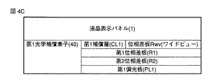
図4Aに示した構成例では、第1補償層CL1は、液晶表示パネル1と第1位相差板R1との間に配置された実質的にAプレート相当の屈折率異方性を有する位相差板RAと、第1位相差板R1と位相差板RAとの間に配置された実質的にCプレート相当の屈折率異方性を有する位相差板RCと、を備えている。
In the configuration example shown in FIG. 4A, the first compensation layer CL1 has a refractive index anisotropy substantially equivalent to the A plate disposed between the liquid
位相差板RAは、ある特定の電圧印加状態(例えば高電圧を印加して黒を表示する状態)での面内での残留リタデーションをキャンセルするように、面内位相差を有している。すなわち、位相差板RAは、その面内方位での互いに直交する方位の屈折率をそれぞれnx及びnyとし、その法線方位の屈折率をnzとしたときに、nx>ny≒nzあるいはnz≒nx>nyの屈折率異方性を有している。このような位相差板RAの作用により、液晶層30の面内位相差がキャンセルされ、画面を正面(画面の法線方向)から観察したときの表示品位を改善する(特にコントラストを向上する)ことが可能となる。
The phase difference plate RA has an in-plane phase difference so as to cancel in-plane residual retardation in a specific voltage application state (for example, a state where black is displayed by applying a high voltage). That is, the retardation plate RA has nx> ny≈nz or nz≈, where nx and ny are the refractive indexes in the directions perpendicular to each other in the in-plane direction, and nz is the refractive index in the normal direction. It has a refractive index anisotropy of nx> ny. Due to the action of the retardation plate RA, the in-plane retardation of the
また、位相差板RCは、ある特定の電圧印加状態(例えば高電圧を印加して黒を表示する状態)での法線方向での残留リタデーションをキャンセルするように、法線位相差を有している。すなわち、位相差板RCは、nx≒ny≠nzの屈折率異方性を有している。このような位相差板RCの作用により、液晶層30の法線位相差がキャンセルされ、画面を斜め方向から観察したときの表示品位を改善する(特に視野角を拡大する)ことが可能となる。
Further, the phase difference plate RC has a normal phase difference so as to cancel the residual retardation in the normal direction in a specific voltage application state (for example, a state where black is displayed by applying a high voltage). ing. That is, the phase difference plate RC has a refractive index anisotropy of nx≈ny ≠ nz. By such an action of the retardation plate RC, the normal phase difference of the
図4Bに示した構成例では、第1補償層CL1は、液晶表示パネル1と第1位相差板R1との間に、2軸の屈折率異方性を有する位相差板RBを備えている。この位相差板RBは、実質的にAプレート相当の屈折率異方性と、実質的にCプレート相当の屈折率異方性とを併せ持っており、より具体的には、nx>ny>nzの屈折率異方性を有している。このような構成例においても、図4Aに示した構成例と同様の効果が得られるとともに、図4Aに示した構成例よりも位相差板の数が減るため、薄型化が可能となる。
In the configuration example shown in FIG. 4B, the first compensation layer CL1 includes a retardation plate RB having biaxial refractive index anisotropy between the liquid
図4Cに示した構成例では、第1補償層CL1は、液晶表示パネル1と第1位相差板R1との間に、位相差板Rwvを備えている。この位相差板Rwvは、液晶層30のリタデーションを補償する異方性フィルムであり、位相差板Rwv自身の総合的な屈折率異方性を考慮したときに、実質的な主軸が法線に対して傾いた屈折率異方性を有する異方性フィルムである。このような位相差板Rwvとしては、例えばWV(ワイドビュー)フィルム(富士写真フィルム(株)製)が適用可能である。このWVフィルムは、光学的に負の1軸性の屈折率異方性を有するディスコティック液晶分子を液晶状態において光軸を法線方向に沿ってハイブリッド配向した状態(つまり、主軸がハイブリッド配向した状態)で固定化させた液晶フィルムである。
In the configuration example illustrated in FIG. 4C, the first compensation layer CL1 includes a retardation plate Rwv between the liquid
特に、OCBモードの液晶表示パネル1に対して第1補償層CL1及び第2補償層CL2がともに位相差板Rwvによって構成された場合、図5に示すように、位相差板Rwvを構成するディスコティック液晶分子は、ベンド配列している各液晶分子31について個々に光学補償する。このため、OCBモードの液晶表示パネル1と位相差板Rwvとの組み合わせは光学補償の観点から有効である。
In particular, when both the first compensation layer CL1 and the second compensation layer CL2 are constituted by the retardation plate Rwv with respect to the OCB mode liquid
図4Dに示した構成例では、第1補償層CL1は、液晶表示パネル1と第1位相差板R1との間に、実質的にAプレート相当の屈折率異方性を有する位相差板RAを備えている。この場合、第1位相差板R1は、2軸の屈折率異方性を有するものを適用する。すなわち、第1位相差板R1の屈折率異方性は、本来の1/4波長板としての機能に加え、実質的にCプレート相当の屈折率異方性を有するように設定され、より具体的には、nx>ny>nzの屈折率異方性を有している。このような構成例においても、図4Aに示した構成例と同様の効果が得られるとともに、図4Aに示した構成例よりも位相差板の数が減るため、薄型化が可能となる。
In the configuration example shown in FIG. 4D, the first compensation layer CL1 is provided between the liquid
上述したような液晶表示装置においては、アレイ基板10側の配向膜16及び対向基板20側の配向膜23のラビング方向を基準方位として、各構成は以下のような軸角度で配置されている。軸角度とは、偏光板の吸収軸及び位相差板の遅相軸(または光軸)が基準方位(X軸)に対して反時計回りになす角度であり、図6によって定義されるものである。すなわち、対向基板20側から液晶表示装置を観察したとき、アレイ基板10(または対向基板20)の主面に平行な平面内において、便宜上、互いに直交するX軸及びY軸を定義し、この平面の法線方向をZ軸と定義する。面内とは、X軸及びY軸で規定される平面内に相当する。
In the liquid crystal display device as described above, the respective components are arranged at the following axis angles with the rubbing direction of the
ここでは、第1構成例の第1光学補償素子40及び第2光学補償素子50において、第1補償層CL1及び第2補償層CL2がそれぞれ図4Aに示したような位相差板RA及び位相差板RCによって構成された場合について説明する。
Here, in the first
すなわち、液晶表示パネル1において、ラビング方向は0°方位に設定されている。第1光学補償素子40においては、第1偏光板PL1はその吸収軸が45°方位に設定され、第1位相差板R1はその遅相軸が0°方位(第1偏光板PL1の吸収軸と略45°で交差)に設定され、第2位相差板R2はそのX−Y平面内の光軸が45°方位(第1偏光板PL1の吸収軸と略平行)に設定され、位相差板RAはその遅相軸が90°方位に設定されている。
That is, in the liquid
第2光学補償素子50においては、第2偏光板PL2はその吸収軸が135°方位に設定され、第3位相差板R3はその遅相軸が90°方位(第2偏光板PL2の吸収軸と略45°で交差)に設定され、第4位相差板R4はそのX−Y平面内の光軸が45°方位(偏光板PLの吸収軸と略直交)に設定され、位相差板RAはその遅相軸が90°方位に設定されている。
In the second
各構成の軸角度をまとめると、図7のようになる。 The shaft angles of the respective configurations are summarized as shown in FIG.
このようなOCBモードを適用した液晶表示装置においては、図6に示したように、X−Z平面内において所定の電圧印加状態(例えば黒表示状態)で液晶分子31がベンド配向している。このような液晶分子31について、X−Y平面内の90°方位から画面を観察した場合には液晶分子31が下(アレイ基板側)から上(対向基板側)に向かって反時計回り(すなわち左回り)に配列しているのに対して、X−Y平面内の270°方位から画面を観察した場合には液晶分子31が下から上に向かって時計回り(すなわち右回り)に配列している。
In the liquid crystal display device to which such an OCB mode is applied, as shown in FIG. 6, the
このため、液晶層30を通過する光の旋光性は、90°方位と270°方位とでは逆回りの液晶分子31の配列によって影響を受ける。このような旋光性の非対称性の影響により、それぞれの方位に向かって液晶層30を通過する光の偏光状態が異なる。つまり、画面の法線方向(すなわちZ軸方向)からX−Y平面内の90°方位に向かって視角を増大していく場合と、X−Y平面内の270°方位に向かって視角を増大していく場合とでは、液晶層30を通過する光の偏光状態の差に起因して画面の表示品位に差が生ずるため、高コントラストが得られる視野角が制限される。
For this reason, the optical rotation of the light passing through the
そこで、この実施の形態においては、液晶層30を通過する光の方位によって異なる旋光性の影響により異なる偏光状態の差を光学的に補償する。
Therefore, in this embodiment, a difference in polarization state that is different due to the influence of optical rotation that varies depending on the direction of light passing through the
更に、所定の電圧印加状態(黒表示状態)においては、液晶層30のみならず他の構成のリタデーションの影響により、第2光学補償素子50の第3位相差板R3を通過した後の光の偏光状態(理想的には直線偏光の偏光状態)が第2偏光板PL2の吸収軸方位からずれる。このため、黒表示の画面の透過率を十分に低下させることができず、コントラストの低下を招くことがある。そこで、第3位相差板R3を通過した光の偏光状態の第2偏光板PL2の吸収軸方位からのずれを光学的に補償する機能を有する光学補償素子を適用している。これにより、コントラストを向上することが可能であるとともに、高コントラストが得られる視野角を拡大することが可能となる。
Further, in a predetermined voltage application state (black display state), the light after passing through the third retardation plate R3 of the second
以下に、より具体的に説明する。 More specific description will be given below.
すなわち、透過型液晶表示装置において第1構成例の第1光学補償素子40及び第2光学補償素子50を適用した場合には、図1に示したように、第1光学補償素子40は第1位相差板R1と第1偏光板PL1との間に2軸の屈折率異方性を有する第2位相差板R2を備え、また、第2光学補償素子50は第3位相差板R3と第2偏光板PL2との間に、2軸の屈折率異方性を有する第4位相差板R4を備えている。発明者は、このような2軸の第2位相差板R2及び第4位相差板R4において、Nz=(nx−nz)/(nx−ny)で与えられるNz係数を最適化することによって上述したような光学的な補償が可能であることを見出した。
That is, when the first
そして、特にこのNz係数の最適な範囲を規定するにあたり、Nz係数を変化させることにより、異なる旋光性の影響や偏光状態の吸収軸方位からのずれの影響を改善することが可能であることが検証された。 In particular, in defining the optimum range of the Nz coefficient, by changing the Nz coefficient, it is possible to improve the influence of different optical rotations and the influence of deviation of the polarization state from the absorption axis direction. Verified.
図1に示した構成においては、第1光学補償素子40の第2位相差板R2は、主に、液晶層30を通過する光の方位によって、主として旋光性の影響による異なる偏光状態の差を補償する。また、第2光学補償素子50の第4位相差板R4は、主に、第3位相差板R3を通過した光の偏光状態の第2偏光板PL2の吸収軸方位からのずれを補償する。
In the configuration shown in FIG. 1, the second retardation plate R2 of the first
このような構成においては、それぞれの補償に必要なNz係数が異なり、第1光学補償素子40の第2位相差板R2及び第2光学補償素子50の第4位相差板R4のそれぞれのNz係数は異なる。具体的には、液晶層30を通過する光の方位によって異なる偏光状態の差を補償するためには、0.7以上0.9以下の範囲のNz係数に設定された第2位相差板R2を適用することが望ましい。このNz係数が0.7よりも小さい、あるいは0.9よりも大きいと、例えば90°方位における視野角コントラストが確保し難い。
In such a configuration, the Nz coefficients necessary for each compensation are different, and the respective Nz coefficients of the second retardation plate R2 of the first
また、第3位相差板R3を通過した光の偏光状態の第2偏光板PL2の吸収軸方位からのずれを補償するためには、0.15以上0.3以下の範囲のNz係数に設定された第4位相差板R4を適用することが望ましい。このNz係数が0.15よりも小さい、あるいは0.3よりも大きいと、やはり偏光状態のずれの補償が不十分となり、視野角コントラストが確保し難い。 Further, in order to compensate for the deviation of the polarization state of the light that has passed through the third retardation plate R3 from the absorption axis direction of the second polarizing plate PL2, the Nz coefficient is set in the range of 0.15 to 0.3. It is desirable to apply the fourth retardation plate R4. When the Nz coefficient is smaller than 0.15 or larger than 0.3, the compensation of the polarization state deviation is still insufficient, and it is difficult to secure the viewing angle contrast.
これにより、十分に広い視野角を得ることが可能となり、良好な表示品位が得られる。 Thereby, a sufficiently wide viewing angle can be obtained, and a good display quality can be obtained.
次に、上述した透過型液晶表示装置において第1構成例の第1光学補償素子40及び第2光学補償素子50を適用した場合の効果を検証した。ここで、本実施形態の透過型液晶表示装置の構成としては、図1に示した通りであり、第1光学補償素子40の第2位相差板R2におけるNz係数は0.9(nx=1.580951、ny=1.578995、nz=1.579191)とし、第2光学補償素子50の第4位相差板R4におけるNz係数は0.2(nx=1.580951、ny=1.578995、nz=1.580560)とした。なお、比較例の液晶表示装置として、第2位相差板を備えていない第1光学補償素子40及び第4位相差板を備えていない第2光学補償素子50を適用し、他の構成は本実施形態と同一とした。
Next, the effect of applying the first
図8Aは、比較例の液晶表示装置におけるコントラスト比の視野角依存性をシミュレーションした結果を示したものである。ここで、中心は液晶表示パネルの法線方向(Z軸)に相当し、法線方向を中心とした同心円は、法線に対する傾き角度(視角)であり、それぞれ20°、40°、60°、80°に相当する。ここで示した特性図は、各方位についてコントラスト比(CR)が100:1から10:1に相当する領域を各々結ぶことで得られたものである。 FIG. 8A shows the result of simulating the viewing angle dependence of the contrast ratio in the liquid crystal display device of the comparative example. Here, the center corresponds to the normal direction (Z axis) of the liquid crystal display panel, and the concentric circles centering on the normal direction are inclination angles (viewing angles) with respect to the normal, which are 20 °, 40 °, and 60 °, respectively. , Corresponding to 80 °. The characteristic diagram shown here is obtained by connecting regions corresponding to contrast ratios (CR) of 100: 1 to 10: 1 for each direction.
図8Aに示したように、比較例の液晶表示装置では、特に、0°方位及び180°方位において、視角が60°以上ではコントラスト比が10:1以下になることがわかる。便宜上、ラビング方向に平行な方位(0°−180°方位)を画面の垂直方向とし、90°方位を画面の右側とし、270°方位を画面の左側とすると、法線方向から画面の上下方向に視角が増大するにともなって、コントラスト比が伴い著しく低下することが確認された。 As shown in FIG. 8A, in the liquid crystal display device of the comparative example, it can be seen that the contrast ratio is 10: 1 or less especially at the viewing angle of 60 ° or more in the 0 ° azimuth and 180 ° azimuth. For convenience, if the azimuth parallel to the rubbing direction (0 ° -180 ° azimuth) is the vertical direction of the screen, 90 ° azimuth is the right side of the screen, and 270 ° azimuth is the left side of the screen, the normal direction and the vertical direction of the screen It was confirmed that as the viewing angle increased, the contrast ratio significantly decreased.
図8Bは、本実施形態の液晶表示装置におけるコントラスト比の視野角依存性をシミュレーションした結果を示したものである。図8Bから明らかなように、画面の全方位について、視角が80°以上の範囲でコントラスト比10:1以上が得られ、十分な視野角が得られることが確認できた。 FIG. 8B shows the result of simulating the viewing angle dependence of the contrast ratio in the liquid crystal display device of the present embodiment. As is clear from FIG. 8B, it was confirmed that a contrast ratio of 10: 1 or more was obtained in a range where the viewing angle was 80 ° or more, and a sufficient viewing angle was obtained in all directions of the screen.
本実施形態の透過型液晶表示装置の他の構成として、第1光学補償素子40の第2位相差板R2におけるNz係数を0.8(nx=1.580951、ny=1.578995、nz=1.579386)とし、第2光学補償素子50の第4位相差板R4におけるNz係数を0.15(nx=1.580951、ny=1.578995、nz=1.580658)とした場合も、同様の効果を確認することができた。
As another configuration of the transmissive liquid crystal display device of this embodiment, the Nz coefficient in the second retardation plate R2 of the first
また、本実施形態の透過型液晶表示装置の他の構成として、第1光学補償素子40の第2位相差板R2におけるNz係数を0.7(nx=1.580951、ny=1.578995、nz=1.579582)とし、第2光学補償素子50の第4位相差板R4におけるNz係数を0.3(nx=1.580951、ny=1.578995、nz=1.580364)とした場合も、同様の効果を確認することができた。
As another configuration of the transmissive liquid crystal display device of the present embodiment, the Nz coefficient in the second retardation plate R2 of the first
しかしながら、第1光学補償素子40の第2位相差板R2におけるNz係数を0.5(nx=1.580951、ny=1.578995、nz=1.579973)とした場合は、不所望な旋光性の影響を補償することができず、高い視野角コントラストの確保はできなかった。第1光学補償素子40の第2位相差板R2におけるNz係数を1.1(nx=1.580951、ny=1.578995、nz=1.58799)とした場合も、同様に不所望な旋光性の影響を補償することができず、高い視野角コントラストの確保はできなかった。
However, when the Nz coefficient in the second retardation plate R2 of the first
なお、図7に示したように、第1構成例においては、第1光学補償素子40において第1偏光板PL1の吸収軸と第2位相差板R2の光軸とが略一致し、また、第2光学補償素子50において第2偏光板PL2の吸収軸と第4位相差板R4の光軸とが略直交する場合について説明したが、この例に限らない。すなわち、液晶表示パネル1について第1光学補償素子40及び第2光学補償素子50は対称な構成であるため、実質的に入れ替えたような構成であっても良い。
As shown in FIG. 7, in the first configuration example, in the first
より具体的には、変形例1においては、第1光学補償素子40において、第2位相差板R2はそのX−Y平面内の光軸が135°方位に設定されている。すなわち、第1偏光板PL1の吸収軸と第2位相差板R2の光軸とは、略直交している。また、第2光学補償素子50において、第4位相差板R4はそのX−Y平面内の光軸が135°方位に設定されている。すなわち、第2偏光板PL2の吸収軸と第4位相差板R4の光軸とは、略一致している。このような変形例1においては、0.7以上0.9以下の範囲のNz係数に設定された第4位相差板R4を適用し、0.15以上0.3以下の範囲のNz係数に設定された第2位相差板R2を適用することにより、上述した第1構成例と同様の効果が得られる。
More specifically, in the first modification, in the first
例えば、第1光学補償素子40の第2位相差板R2におけるNz係数を0.2とし、第2光学補償素子50の第4位相差板R4におけるNz係数を0.8とした場合には、十分な視野角が得られることが確認できた。
For example, when the Nz coefficient in the second retardation plate R2 of the first
また、このような第1構成例においては、第1光学補償素子40において第1偏光板PL1の吸収軸と第2位相差板R2の光軸とが略一致し、また、第2光学補償素子50において第2偏光板PL2の吸収軸と第4位相差板R4の光軸とが略一致する場合、ともに0.7以上0.9以下の範囲のNz係数に設定された第2位相差板R2及び第4位相差板R4を適用すればよい。同様に、第1光学補償素子40において第1偏光板PL1の吸収軸と第2位相差板R2の光軸とが略直交し、また、第2光学補償素子50において第2偏光板PL2の吸収軸と第4位相差板R4の光軸とが略直交する場合、ともに0.15以上0.3以下の範囲のNz係数に設定された第2位相差板R2及び第4位相差板R4を適用すればよい。これらの各場合においても、上述した第1構成例と同様の効果が得られるとともに、部材を共通化することができ、低コスト化が可能となる。
In such a first configuration example, in the first
《光学補償素子の第2構成例》
第2構成例において、第1光学補償素子40及び第2光学補償素子50は、上述した第1構成例と同様に、液晶表示パネル1における液晶層30に電圧を印加した所定の表示状態において、液晶層30のリタデーションを光学的に補償する機能を有している。
<< Second Configuration Example of Optical Compensation Element >>
In the second configuration example, the first
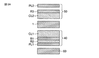
すなわち、図9Aに示すように、アレイ基板10の外面に配置された第1光学補償素子40は、第1偏光板PL1、第1位相差板R1、第2位相差板R2などを備えて構成されている。対向基板20の外面に配置された第2光学補償素子50は、第2偏光板PL2、第3位相差板R3などを備えて構成されている。これらの第1光学補償素子40及び第2光学補償素子50は、液晶表示パネル1について非対称な構成となっている。このような第2構成例の光学補償素子を適用した液晶表示装置によれば、第1構成例の光学補償素子を適用した液晶表示装置と比較して、位相差板の数が減るため、低コスト化及び薄型化が可能となる。
That is, as shown in FIG. 9A, the first
第1偏光板PL1及び第2偏光板PL2、及び、第1位相差板R1及び第3位相差板R3は、第1構成例と同一である。すなわち、第1偏光板PL1と第1位相差板(1/4波長板)R1との組み合わせ、及び、第2偏光板PL2と第3位相差板(1/4波長板)R3との組み合わせは、理想的には偏光板の透過軸を透過した所定波長の直線偏光を円偏光に変換する円偏光素子として機能する。 The first polarizing plate PL1, the second polarizing plate PL2, the first retardation plate R1, and the third retardation plate R3 are the same as in the first configuration example. That is, the combination of the first polarizing plate PL1 and the first retardation plate (1/4 wavelength plate) R1 and the combination of the second polarizing plate PL2 and the third retardation plate (1/4 wavelength plate) R3 are Ideally, it functions as a circularly polarizing element that converts linearly polarized light having a predetermined wavelength transmitted through the transmission axis of the polarizing plate into circularly polarized light.
第2位相差板R2は、第1偏光板PL1と第1位相差板R1との間に配置されている。この第2位相差板R2は、2軸の屈折率異方性を有する位相差板である。 The second retardation plate R2 is disposed between the first polarizing plate PL1 and the first retardation plate R1. The second retardation plate R2 is a retardation plate having biaxial refractive index anisotropy.
また、第1光学補償素子40は、液晶表示パネル1と第1位相差板R1との間に配置された第1補償層CL1を備えている。また、第2光学補償素子50は、液晶表示パネル1と第3位相差板R3との間に配置された第2補償層CL2を備えている。これらの第1補償層CL1及び第2補償層CL2を含む第1光学補償素子40及び第2光学補償素子50の構成について、第1構成例と同様に、図4A乃至図4Dに示したような構成例を適用可能である。
The first
第2構成例の第1光学補償素子40及び第2光学補償素子50において、第1補償層CL1及び第2補償層CL2がそれぞれ図4Aに示したような位相差板RA及び位相差板RCによって構成された場合について説明する。
In the first
すなわち、液晶表示パネル1において、ラビング方向は0°方位に設定されている。第1光学補償素子40においては、第1偏光板PL1はその吸収軸が45°方位に設定され、第1位相差板R1はその遅相軸が0°方位(第1偏光板PL1の吸収軸と略45°で交差)に設定され、第2位相差板R2はそのX−Y平面内の光軸が45°方位(第1偏光板PL1の吸収軸と略平行)に設定され、位相差板RAはその遅相軸が90°方位に設定されている。
That is, in the liquid
第2光学補償素子50においては、第2偏光板PL2はその吸収軸が135°方位に設定され、第3位相差板R3はその遅相軸が90°方位(第2偏光板PL2の吸収軸と略45°で交差)に設定され、位相差板RAはその遅相軸が90°方位に設定されている。
In the second
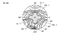
各構成の軸角度をまとめると、図10Aのようになる。 FIG. 10A shows the shaft angles of the respective configurations.
この第2構成例においても、第1構成例と同様に、液晶層30を通過する光の方位によって異なる旋光性の影響により異なる偏光状態の差を光学的に補償するとともに、第3位相差板R3を通過した光の偏光状態の第2偏光板PL2の吸収軸方位からのずれを光学的に補償する機能を有する光学補償素子を適用している。これにより、コントラストを向上することが可能であるとともに、高コントラストが得られる視野角を拡大することが可能となる。
In the second configuration example, as in the first configuration example, the difference in polarization state due to the influence of optical rotation that varies depending on the direction of light passing through the
以下に、より具体的に説明する。 More specific description will be given below.
すなわち、透過型液晶表示装置において第2構成例の第1光学補償素子40及び第2光学補償素子50を適用した場合には、図9Aに示したように、第1光学補償素子40は第1位相差板R1と第1偏光板PL1との間に2軸の屈折率異方性を有する第2位相差板R2を備えている。図9Aに示した構成においては、第1光学補償素子40の第2位相差板R2は、液晶層30を通過する光の方位によって、旋光性の影響による異なる偏光状態の差を補償するとともに、第3位相差板R3を通過した光の偏光状態の第2偏光板PL2の吸収軸方位からのずれを補償する機能を有している。
That is, when the first
このような構成においては、0.4以上0.6以下の範囲のNz係数に設定された第2位相差板R2を適用することが望ましい。このNz係数が0.4よりも小さい、あるいは0.6よりも大きいと、光学補償が不十分となり視野角コントラストが確保し難い。 In such a configuration, it is desirable to apply the second retardation plate R2 set to an Nz coefficient in the range of 0.4 to 0.6. If this Nz coefficient is smaller than 0.4 or larger than 0.6, the optical compensation becomes insufficient and it is difficult to secure the viewing angle contrast.
これにより、十分に広い視野角を得ることが可能となり、良好な表示品位が得られる。 Thereby, a sufficiently wide viewing angle can be obtained, and a good display quality can be obtained.
次に、上述した透過型液晶表示装置において第2構成例の第1光学補償素子40及び第2光学補償素子50を適用した場合の効果を検証した。ここで、本実施形態の透過型液晶表示装置の構成としては、図9Aに示した通りであり、第1光学補償素子40の第2位相差板R2におけるNz係数は0.5(nx=1.580951、ny=1.578995、nz=1.579973)とした。本実施形態の液晶表示装置におけるコントラスト比の視野角依存性をシミュレーションしたところ、図10Bに示すように、画面の全方位について、視角が60°以上の範囲でコントラスト比10:1以上が得られ、また90°方位を除いては、視角が80°以上の範囲でコントラスト比10:1以上が得られ、十分な視野角が得られることが確認できた。
Next, the effect of applying the first
なお、図10Aに示したように、第2構成例においては、第1光学補償素子40において第1偏光板PL1と第1位相差板R1との間に第2位相差板R2を配置し、第1偏光板PL1の吸収軸と第2位相差板R2の光軸とが略一致する場合について説明したが、この例に限らない。すなわち、液晶表示パネル1について第1光学補償素子40及び第2光学補償素子50を実質的に入れ替えたような構成であっても良い。
As shown in FIG. 10A, in the second configuration example, in the first
より具体的には、変形例2においては、図9B及び図10Aに示すように、第1光学補償素子40においては、第2位相差板R2を配置せず、第2光学補償素子50において、第2偏光板PL2と第3位相差板R3との間に第2位相差板R2を配置する。この第2位相差板R2はそのX−Y平面内の光軸が135°方位に設定されている。すなわち、第2偏光板PL2の吸収軸と第2位相差板R2の光軸とは、略一致している。このような変形例2においても、0.4以上0.6以下の範囲のNz係数に設定された第2位相差板R2を適用することにより、上述した第2構成例と同様の効果が得られる。
More specifically, in the second modification, as shown in FIGS. 9B and 10A, the first
例えば、第2光学補償素子50の第2位相差板R2におけるNz係数を0.5とした場合には、十分な視野角が得られることが確認できた。
For example, it was confirmed that when the Nz coefficient in the second retardation plate R2 of the second
このような第2構成例においては、第1光学補償素子40に第2位相差板R2を配置し、第1偏光板PL1の吸収軸と第2位相差板R2の光軸とが略直交する場合(例えば第1偏光板PL1の吸収軸を45°方位に設定し、第2位相差板R2のX−Y平面内の光軸を135°方位に設定した場合)、及び、第2光学補償素子50に第2位相差板R2を配置し、第2偏光板PL2の吸収軸と第2位相差板R2の光軸とが略直交する場合(例えば第2偏光板PL2の吸収軸を135°方位に設定し、第2位相差板R2のX−Y平面内の光軸を45°方位に設定した場合)には、ともに0.4以上0.6以下の範囲のNz係数に設定された第2位相差板R2を適用すればよい。これらの各場合においても、上述した第2構成例と同様の効果が得られる。
In such a second configuration example, the second retardation plate R2 is disposed in the first
また、上述した第1構成例及び第2構成例において、第1補償層CL1及び第2補償層CL2の少なくとも一方において、図4Bに示したような構成例を適用する場合、位相差板RBはそのX−Y平面内の光軸を90°方位に設定することにより同様の効果が得られる。 In the first configuration example and the second configuration example described above, when the configuration example as illustrated in FIG. 4B is applied to at least one of the first compensation layer CL1 and the second compensation layer CL2, the retardation plate RB A similar effect can be obtained by setting the optical axis in the XY plane to a 90 ° azimuth.
例えば、第1構成例において、第1補償層CL1及び第2補償層CL2が位相差板RBによって構成され、位相差板RBにおけるそれぞれのNz係数を4.8とするとともにそれぞれのリタデーションReを90nmとし、第1光学補償素子40の第2位相差板R2におけるNz係数を0.2とし、第2光学補償素子50の第4位相差板R4におけるNz係数を0.8とした場合には、図10Cに示すように、十分な視野角が得られることが確認できた。
For example, in the first configuration example, the first compensation layer CL1 and the second compensation layer CL2 are configured by the phase difference plate RB, each Nz coefficient in the phase difference plate RB is set to 4.8, and each retardation Re is set to 90 nm. When the Nz coefficient in the second retardation plate R2 of the first
例えば、第2構成例において、第1補償層CL1及び第2補償層CL2が位相差板RBによって構成され、第2光学補償素子50の第2位相差板R2におけるNz係数を0.5とした場合には、十分な視野角が得られることが確認できた。
For example, in the second configuration example, the first compensation layer CL1 and the second compensation layer CL2 are configured by the phase difference plate RB, and the Nz coefficient in the second phase difference plate R2 of the second
また、第1構成例及び第2構成例において、第1補償層CL1及び第2補償層CL2の少なくとも一方において、図4Cに示したような構成例を適用する場合、位相差板RwvはそのX−Y平面内の光軸を0°方位に設定することにより同様の効果が得られる。 Further, in the first configuration example and the second configuration example, when the configuration example as illustrated in FIG. 4C is applied to at least one of the first compensation layer CL1 and the second compensation layer CL2, the retardation plate Rwv has its X A similar effect can be obtained by setting the optical axis in the −Y plane to 0 ° azimuth.
また、第1構成例及び第2構成例において、第1光学補償素子40及び第2光学補償素子50の少なくとも一方において、図4Dに示したような構成例を適用する場合、第1位相差板R1はそのX−Y平面内の光軸を0°方位に設定し、また、位相差板RAはそのX−Y平面内の光軸を90°方位に設定することにより同様の効果が得られる。
In the first configuration example and the second configuration example, when the configuration example as shown in FIG. 4D is applied to at least one of the first
《半透過型液晶表示装置》
次に、この実施の形態に係る半透過型液晶表示装置について説明する。この半透過型液晶表示装置の構成は、図11に示した通りである。すなわち、基本構成は、図3に示した透過型液晶表示装置と同様であるが、マトリクス状に配置された複数の表示画素PXのそれぞれが、外光を選択的に反射することによって画像を表示する反射部PRと、バックライト60からのバックライト光を選択的に透過することによって画像を表示する透過部PTと、を有している点で相違する。
<Semi-transmissive liquid crystal display device>
Next, a transflective liquid crystal display device according to this embodiment will be described. The configuration of the transflective liquid crystal display device is as shown in FIG. That is, the basic configuration is the same as that of the transmissive liquid crystal display device shown in FIG. 3, but each of the plurality of display pixels PX arranged in a matrix displays an image by selectively reflecting external light. It is different in that it includes a reflection part PR that transmits light and a transmission part PT that displays an image by selectively transmitting backlight light from the
アレイ基板10において、絶縁層14は、反射部PRと透過部PTとでリタデーションに差を持たせるために液晶層3のギャップ差を形成する。各画素電極13は、反射部PRに対応して設けられた反射電極13R及び透過部PTに対応して設けられた透過電極13Tを有しており、これら電極13R及び13Tは互いに電気的に接続され、共に一つのスイッチング素子Wによって制御される。反射電極13Rは、アルミニウムなどの光反射性を有する導電材料によって形成されている。透過電極13Tは、インジウム・ティン・オキサイド(ITO)などの光透過性を有する導電材料によって形成されている。これらの反射電極13R及び透過電極13Tは、スイッチング素子13と電気的に接続されている。
In the
図11に示した例では、透過部PT及び反射部PRにおいては、液晶層30に電圧を印加した所定の表示状態において、アレイ基板10と対向基板20との間で液晶分子31がベンド配向している。
In the example shown in FIG. 11, in the transmissive portion PT and the reflective portion PR, the
このような半透過型液晶表示装置においても、図1に示した第1構成例及びその変形例1、図9Aに示した第2構成例及び図9Bに示したその変形例2のいずれの構成の第1光学補償素子40及び第2光学補償素子50も適用可能である。また、第1光学補償素子40及び第2光学補償素子50は、図4A乃至図4Dに示したいずれかの構成例を適用可能である。
Also in such a transflective liquid crystal display device, any one of the first configuration example shown in FIG. 1 and its modification example 1, the second configuration example shown in FIG. 9A, and its modification example 2 shown in FIG. 9B. The first
次に、上述した半透過型液晶表示装置において第1構成例の第1光学補償素子40及び第2光学補償素子50を適用した場合の効果を検証した。ここで、本実施形態の半透過型液晶表示装置の構成としては、図1に示した通りであり、アレイ基板10の外面に配置された第1光学補償素子40の第2位相差板R2におけるNz係数は0.9(nx=1.580951、ny=1.578995、nz=1.579191)とし、対向基板20の外面に配置された第2光学補償素子50の第4位相差板R4におけるNz係数は0.2(nx=1.580951、ny=1.578995、nz=1.580560)とした。なお、比較例の半透過型液晶表示装置として、第2位相差板を備えていない第1光学補償素子40及び第4位相差板を備えていない第2光学補償素子50を適用し、他の構成は本実施形態と同一とした。
Next, the effect of applying the first
図12Aに示したように、比較例の半透過型液晶表示装置について、透過部では、特に、0°方位及び180°方位において、視角が60°以上ではコントラスト比が10:1以下になることがわかる。これに対して、図12Bに示したように、本実施形態の半透過型液晶表示装置について、透過部では、画面の全方位について、視角が80°以上の範囲でコントラスト比10:1以上が得られ、比較例に対して十分な視野角が得られることが確認された。 As shown in FIG. 12A, in the transflective liquid crystal display device of the comparative example, in the transmissive part, the contrast ratio is 10: 1 or less particularly in the 0 ° azimuth and 180 ° azimuth when the viewing angle is 60 ° or more. I understand. On the other hand, as shown in FIG. 12B, in the transflective liquid crystal display device of the present embodiment, the transmissive portion has a contrast ratio of 10: 1 or more in a range of viewing angles of 80 ° or more in all directions of the screen. It was confirmed that a sufficient viewing angle was obtained with respect to the comparative example.
図13Aに示したように、比較例の半透過型液晶表示装置について、反射部では、特に、0°方位及び180°方位において、視角が40°以上ではコントラスト比が10:1以下になることがわかる。これに対して、図13Bに示したように、本実施形態の半透過型液晶表示装置について、反射部では、画面の90°−270°方位については、視角が80°以上の範囲でコントラスト比10:1以上が得られ、また、画面の0°−180°方位については、視角が50°以上の範囲でコントラスト比10:1以上が得られ、比較例と比較して視野角を拡大できたことが確認された。 As shown in FIG. 13A, in the transflective liquid crystal display device of the comparative example, the contrast ratio is 10: 1 or less at the reflection portion, particularly in the 0 ° azimuth and 180 ° azimuth when the viewing angle is 40 ° or more. I understand. On the other hand, as shown in FIG. 13B, in the transflective liquid crystal display device of the present embodiment, in the reflection portion, the 90 ° -270 ° azimuth of the screen has a contrast ratio in the range of the viewing angle of 80 ° or more. 10: 1 or more is obtained, and for the 0 ° -180 ° azimuth of the screen, a contrast ratio of 10: 1 or more is obtained in a viewing angle range of 50 ° or more, and the viewing angle can be expanded as compared with the comparative example. It was confirmed that
次に、上述した半透過型液晶表示装置において第2構成例の第1光学補償素子40及び第2光学補償素子50を適用した場合の効果を検証した。ここで、本実施形態の半透過型液晶表示装置の構成としては、図9Aに示した通りであり、アレイ基板10の外面に配置された第1光学補償素子40の第2位相差板R2におけるNz係数は0.5(nx=1.580951、ny=1.578995、nz=1.579973)とした。本実施形態の半透過型液晶表示装置におけるコントラスト比の視野角依存性をシミュレーションしたところ、透過部及び反射部ともに、画面の全方位について、視角が60°以上の範囲でコントラスト比10:1以上が得られ、また透過部においては90°方位を除いては、視角が80°以上の範囲でコントラスト比10:1以上が得られ、十分な視野角が得られることが確認できた。
Next, the effect of applying the first
《反射型液晶表示装置》
次に、この実施の形態に係る反射型液晶表示装置について説明する。この反射型液晶表示装置の構成は、図14に示した通りである。すなわち、基本構成は、図3に示した透過型液晶表示装置と同様であるが、アレイ基板10は、画素電極13として反射電極を備えている点で相違する。各画素電極13は、アルミニウムなどの光反射性を有する導電材料によって形成されている。つまり、各画素PXは、反射部に相当する。
<Reflective LCD>
Next, a reflective liquid crystal display device according to this embodiment will be described. The configuration of the reflective liquid crystal display device is as shown in FIG. That is, the basic configuration is the same as that of the transmissive liquid crystal display device shown in FIG. 3, but the
このような反射型液晶表示装置においては、対向基板20の外面のみに光学補償素子70が配置されている。この光学補償素子70は、偏向板PL、偏向板PLと液晶表示パネル1との間に配置された第1位相差板(1/4波長板)R1、偏向板PLと第1波長板R1との間に配置された2軸の第2位相差板(1/2波長板)R2、第1位相差板R1と液晶表示パネル1との間に配置された補償層CLを備えて構成されている。この光学補償素子70は、図4A乃至図4Dに示したいずれかの構成例を適用可能である。
In such a reflective liquid crystal display device, the
ここでは、光学補償素子70において、補償層CLが図4Aに示したような位相差板RA及び位相差板RCによって構成された場合について説明する。
Here, in the
すなわち、液晶表示パネル1において、ラビング方向は0°方位に設定されている。光学補償素子70においては、偏光板PLはその吸収軸が135°方位に設定され、第2位相差板R2はそのX−Y平面内の光軸が45°方位(偏光板PLの吸収軸と略直交)に設定されている。また、第1位相差板R1はそのX−Y平面内の光軸が90°方位に設定され、位相差板RAはそのX−Y平面内の光軸が90°方位に設定されている。
That is, in the liquid
各構成の軸角度をまとめると、図15のようになる。 The shaft angles of the respective configurations are summarized as shown in FIG.
このような反射型液晶表示装置においても、液晶層30を通過する光の方位によって異なる旋光性の影響により異なる偏光状態の差を光学的に補償するとともに、第1位相差板R1を通過した光の偏光状態の偏光板PLの吸収軸方位からのずれを光学的に補償する機能を有する光学補償素子を適用している。これにより、コントラストを向上することが可能であるとともに、高コントラストが得られる視野角を拡大することが可能となる。
Also in such a reflective liquid crystal display device, the difference in polarization state due to the influence of optical rotation that varies depending on the direction of light passing through the
すなわち、反射型液晶表示装置の光学補償素子70において、第1位相差板R1と偏光板PLとの間に配置された2軸の屈折率異方性を有する第2位相差板R2は、視認側から入射した光に対して、液晶層30を通過する光の方位によって、旋光性の影響による異なる偏光状態の差を補償する。また、この第2位相差板R2は、各画素電極13で反射された光に対しては、第1位相差板R1を通過した光の偏光状態の偏光板PLの吸収軸方位からのずれを補償する。
That is, in the
第2位相差板R2のX−Y平面内の光軸が偏光板PLの吸収軸と略直交するような構成においては、0.15以上0.3以下の範囲のNz係数に設定された第2位相差板R2を適用することが望ましい。このNz係数が0.15よりも小さい、あるいは0.3よりも大きいと、光学補償が不十分となり視野角コントラストが確保し難い。 In the configuration in which the optical axis in the XY plane of the second retardation plate R2 is substantially orthogonal to the absorption axis of the polarizing plate PL, the first Nz coefficient is set in the range of 0.15 to 0.3. It is desirable to apply the two phase difference plate R2. If this Nz coefficient is smaller than 0.15 or larger than 0.3, the optical compensation becomes insufficient and it is difficult to secure the viewing angle contrast.
これにより、十分に広い視野角を得ることが可能となり、良好な表示品位が得られる。 Thereby, a sufficiently wide viewing angle can be obtained, and a good display quality can be obtained.
次に、上述した反射型液晶表示装置において光学補償素子70を適用した場合の効果を検証した。ここで、本実施形態の反射型液晶表示装置の構成としては、図14に示した通りであり、光学補償素子70の第2位相差板R2におけるNz係数は0.2(nx=1.580951、ny=1.578995、nz=1.580560)とした。なお、比較例の反射型液晶表示装置として、第2位相差板を備えていない光学補償素子70を適用し、他の構成は本実施形態と同一とした。
Next, the effect of applying the
図16Aに示したように、比較例の反射型液晶表示装置については、特に、0°方位及び180°方位において、視角が50°以上ではコントラスト比が10:1以下になることがわかる。これに対して、図16Bに示したように、本実施形態の反射型液晶表示装置については、画面の全方位について、視角が80°以上の範囲でコントラスト比10:1以上が得られ、比較例に対して十分な視野角が得られることが確認された。 As shown in FIG. 16A, it can be seen that the contrast ratio of the reflective liquid crystal display device of the comparative example is 10: 1 or less when the viewing angle is 50 ° or more in the 0 ° azimuth and 180 ° azimuth. On the other hand, as shown in FIG. 16B, the reflection type liquid crystal display device of the present embodiment has a contrast ratio of 10: 1 or more in a range of viewing angles of 80 ° or more in all directions of the screen. It was confirmed that a sufficient viewing angle was obtained for the example.
本実施形態の反射型液晶表示装置の他の構成として、光学補償素子70の第2位相差板R2として、Nz係数が0.15(nx=1.580951、ny=1.578995、nz=1.580658)とした場合も、同様の効果を確認することができた。
As another configuration of the reflective liquid crystal display device of the present embodiment, as the second retardation plate R2 of the
また、本実施形態の反射型液晶表示装置の他の構成として、光学補償素子70の第2位相差板R2として、Nz係数が0.3(nx=1.580951、ny=1.578995、nz=1.580364)とした場合も、同様の効果を確認することができた。
Further, as another configuration of the reflective liquid crystal display device of the present embodiment, as the second retardation plate R2 of the
また、比較例としてNz係数が0.5(nx=1.580951、ny=1.578995、nz=1.579973)とした場合は、上記の比較例と同様に、高い視野角コントラストの確保はできなかった。 As a comparative example, when the Nz coefficient is 0.5 (nx = 1.580951, ny = 1.579895, nz = 1.579793), as in the above comparative example, a high viewing angle contrast is ensured. could not.
なお、図15に示したように、構成例においては、光学補償素子70において偏光板PLの吸収軸と第2位相差板R2の光軸とが略直交する場合について説明したが、この例に限らない。より具体的には、変形例においては、光学補償素子70において、第2位相差板R2はそのX−Y平面内の光軸が135°方位に設定されている。すなわち、偏光板PLの吸収軸と第2位相差板R2の光軸とは、略一致している。このような変形例においては、0.7以上0.9以下の範囲のNz係数に設定された第2位相差板R2を適用することにより、上述した構成例と同様の効果が得られる。
As shown in FIG. 15, in the configuration example, the case where the absorption axis of the polarizing plate PL and the optical axis of the second retardation plate R2 are substantially orthogonal to each other in the
なお、この発明は、上記実施形態そのものに限定されるものではなく、その実施の段階ではその要旨を逸脱しない範囲で構成要素を変形して具体化できる。また、上記実施形態に開示されている複数の構成要素の適宜な組み合せにより種々の発明を形成できる。例えば、実施形態に示される全構成要素から幾つかの構成要素を削除してもよい。更に、異なる実施形態に亘る構成要素を適宜組み合せてもよい。 In addition, this invention is not limited to the said embodiment itself, In the stage of implementation, it can change and implement a component within the range which does not deviate from the summary. Further, various inventions can be formed by appropriately combining a plurality of constituent elements disclosed in the embodiment. For example, some components may be deleted from all the components shown in the embodiment. Furthermore, you may combine suitably the component covering different embodiment.
例えば、光学補償素子は、液晶層30の外側に配置されていれば良い。すなわち、アレイ基板10側に光学補償素子を配置する場合には、上述した実施の形態の構成に限らず、アレイ基板10を構成する絶縁基板11と液晶層30との間に光学補償素子を配置しても良い。また、対向基板20側に光学補償素子を配置する場合にも同様に、上述した実施の形態の構成に限らず、対向基板20を構成する絶縁基板21と液晶層30との間に光学補償素子を配置しても良い。
For example, the optical compensation element may be disposed outside the
DSP…アクティブエリア PX…表示画素 R1…第1位相差板 R2…第2位相差板 R3…第3位相差板 R4…第4位相差板 PL…偏光板 1…液晶表示パネル 10…アレイ基板 20…対向基板 30…液晶層 31…液晶分子 40…第1光学補償素子 50…第2光学補償素子 60…バックライト 70…光学補償素子
DSP ... Active area PX ... Display pixel R1 ... First retardation plate R2 ... Second retardation plate R3 ... Third retardation plate R4 ... Fourth retardation plate PL ... Polarizing
Claims (22)
前記液晶層の外側に配置され、前記液晶層に電圧を印加した所定の表示状態において、前記液晶層のリタデーションを光学的に補償する光学補償素子と、を備え、
前記光学補償素子は、
偏光板と、
前記偏光板と前記液晶層との間に配置され、1/4波長の位相差を与える第1位相差板と、
前記偏光板と前記第1位相差板との間に配置された2軸の屈折率異方性を有する第2位相差板と、を含み、
前記第2位相差板は、前記液晶層を通過する光の方位によって異なる旋光性の影響による偏光状態の差を補償するとともに前記第1位相差板を通過した光の偏光状態の前記偏光板の吸収軸方位からのずれを補償するように設定された屈折率異方性を有することを特徴とする液晶表示装置。 A liquid crystal display panel using an OCB mode configured to hold a liquid crystal layer between a first substrate and a second substrate;
An optical compensation element that is disposed outside the liquid crystal layer and optically compensates for retardation of the liquid crystal layer in a predetermined display state in which a voltage is applied to the liquid crystal layer;
The optical compensation element is:
A polarizing plate;
A first retardation plate disposed between the polarizing plate and the liquid crystal layer to give a quarter-wave retardation;
A second retardation plate having biaxial refractive index anisotropy disposed between the polarizing plate and the first retardation plate,
The second retardation plate compensates for a difference in polarization state due to the effect of optical rotation that varies depending on the direction of light passing through the liquid crystal layer, and is also used for the polarization state of the polarizing plate of light that has passed through the first retardation plate. A liquid crystal display device having a refractive index anisotropy set so as to compensate for a deviation from an absorption axis direction.
前記光学補償素子は、前記第2基板の外面に配置されていることを特徴とする請求項1に記載の液晶表示装置。 The liquid crystal display panel includes a reflective electrode on the first substrate,
The liquid crystal display device according to claim 1, wherein the optical compensation element is disposed on an outer surface of the second substrate.
前記光学補償素子は、前記第1基板の外面または前記第2基板の外面に配置されていることを特徴とする請求項1に記載の液晶表示装置。 The liquid crystal display panel includes a transmissive electrode on the first substrate,
The liquid crystal display device according to claim 1, wherein the optical compensation element is disposed on an outer surface of the first substrate or an outer surface of the second substrate.
前記第1位相差板は、進相軸及び遅相軸を透過する所定波長の光の間に1/4波長の位相差を与えるとともに、Cプレート相当の2軸の屈折率異方性を有することを特徴とする請求項1に記載の液晶表示装置。 Furthermore, a retardation plate RA having a refractive index anisotropy equivalent to an A plate is provided between the liquid crystal display panel and the first retardation plate.
The first retardation plate gives a quarter-wave phase difference between light of a predetermined wavelength that passes through the fast axis and the slow axis, and has biaxial refractive index anisotropy equivalent to a C plate. The liquid crystal display device according to claim 1.
前記液晶層の外側にそれぞれ配置され、前記液晶層に電圧を印加した所定の表示状態において、前記液晶層のリタデーションを光学的に補償する第1光学補償素子及び第2光学補償素子と、を備え、
前記第1光学補償素子は、
第1偏光板と、
前記第1偏光板と前記液晶層との間に配置され、1/4波長の位相差を与える第1位相差板と、
前記第1偏光板と前記第1位相差板との間に配置された2軸の屈折率異方性を有する第2位相差板と、を含み、
前記第2光学補償素子は、
第2偏光板と、
前記第2偏光板と前記液晶層との間に配置され、1/4波長の位相差を与える第3位相差板と、
前記第2偏光板と前記第3位相差板との間に配置された2軸の屈折率異方性を有する第4位相差板と、を含み、
前記第2位相差板及び前記第4位相差板は、前記液晶層を通過する光の方位によって異なる旋光性の影響による偏光状態の差を補償するとともに前記第1位相差板を通過した光の偏光状態の前記偏光板の吸収軸方位からのずれを補償するように設定された屈折率異方性を有することを特徴とする液晶表示装置。 A liquid crystal display panel using an OCB mode configured to hold a liquid crystal layer between a first substrate and a second substrate;
A first optical compensation element and a second optical compensation element that are respectively arranged outside the liquid crystal layer and optically compensate for retardation of the liquid crystal layer in a predetermined display state in which a voltage is applied to the liquid crystal layer. ,
The first optical compensation element includes:
A first polarizing plate;
A first retardation plate disposed between the first polarizing plate and the liquid crystal layer to give a quarter-wave retardation;
A second retardation plate having a biaxial refractive index anisotropy disposed between the first polarizing plate and the first retardation plate,
The second optical compensation element is:
A second polarizing plate;
A third retardation plate disposed between the second polarizing plate and the liquid crystal layer and providing a quarter-wave retardation;
A fourth retardation plate having a biaxial refractive index anisotropy disposed between the second polarizing plate and the third retardation plate,
The second retardation plate and the fourth retardation plate compensate for the difference in polarization state caused by the effect of optical rotation that varies depending on the direction of light passing through the liquid crystal layer, and the light that has passed through the first retardation plate. A liquid crystal display device having a refractive index anisotropy set so as to compensate for a deviation of the polarization state from the absorption axis direction of the polarizing plate.
前記第2位相差板は、その面内での互いに直交する方位の屈折率をそれぞれnx及びnyとし、その法線方向の屈折率をnzとしたときに、Nz=(nx−nz)/(nx−ny)で与えられるNz係数が0.7以上0.9以下に設定され、
前記第4位相差板のNz係数が0.15以上0.3以下に設定されたことを特徴とする請求項14に記載の液晶表示装置。 The absorption axis of the first polarizing plate and the optical axis of the second retardation plate are substantially coincident, and the absorption axis of the second polarizing plate and the optical axis of the fourth retardation plate are substantially orthogonal,
The second retardation plate has Nz = (nx−nz) / (Nz = (nx−nz) / (), where nx and ny are the refractive indexes in the directions perpendicular to each other in the plane, and nz is the refractive index in the normal direction. nx−ny) is set to 0.7 or more and 0.9 or less,
The liquid crystal display device according to claim 14, wherein an Nz coefficient of the fourth retardation plate is set to 0.15 or more and 0.3 or less.
前記第2位相差板は、その面内での互いに直交する方位の屈折率をそれぞれnx及びnyとし、その法線方向の屈折率をnzとしたときに、Nz=(nx−nz)/(nx−ny)で与えられるNz係数が0.15以上0.3以下に設定され、
前記第4位相差板のNz係数が0.7以上0.9以下に設定されたことを特徴とする請求項14に記載の液晶表示装置。 The absorption axis of the first polarizing plate and the optical axis of the second retardation plate are substantially orthogonal, and the absorption axis of the second polarizing plate and the optical axis of the fourth retardation plate are substantially coincided with each other.
The second retardation plate has Nz = (nx−nz) / (Nz = (nx−nz) / (), where nx and ny are the refractive indexes in the directions perpendicular to each other in the plane, and nz is the refractive index in the normal direction. nx−ny) is set to be 0.15 or more and 0.3 or less,
The liquid crystal display device according to claim 14, wherein an Nz coefficient of the fourth retardation plate is set to 0.7 or more and 0.9 or less.
前記第2位相差板及び前記第4位相差板は、それぞれの面内での互いに直交する方位の屈折率をそれぞれnx及びnyとし、その法線方向の屈折率をnzとしたときに、Nz=(nx−nz)/(nx−ny)で与えられるNz係数が0.15以上0.3以下に設定されたことを特徴とする請求項14に記載の液晶表示装置。 The absorption axis of the first polarizing plate and the optical axis of the second retardation plate are substantially orthogonal, and the absorption axis of the second polarizing plate and the optical axis of the fourth retardation plate are substantially orthogonal;
The second retardation plate and the fourth retardation plate have a refractive index of nz and ny in directions perpendicular to each other in their respective planes, and Nz when the refractive index in the normal direction is nz. 15. The liquid crystal display device according to claim 14, wherein an Nz coefficient given by = (nx−nz) / (nx−ny) is set to 0.15 or more and 0.3 or less.
前記第2位相差板及び前記第4位相差板は、それぞれの面内での互いに直交する方位の屈折率をそれぞれnx及びnyとし、その法線方向の屈折率をnzとしたときに、Nz=(nx−nz)/(nx−ny)で与えられるNz係数が0.7以上0.9以下に設定されたことを特徴とする請求項14に記載の液晶表示装置。 The absorption axis of the first polarizing plate and the optical axis of the second retardation plate substantially coincide with each other, and the absorption axis of the second polarizing plate and the optical axis of the fourth retardation plate substantially coincide with each other.
The second retardation plate and the fourth retardation plate have a refractive index of nz and ny in directions perpendicular to each other in their respective planes, and Nz when the refractive index in the normal direction is nz. The liquid crystal display device according to claim 14, wherein an Nz coefficient given by = (nx−nz) / (nx−ny) is set to 0.7 or more and 0.9 or less.
前記第1位相差板及び第3位相差板のそれぞれは、進相軸及び遅相軸を透過する所定波長の光の間に1/4波長の位相差を与えるとともに、Cプレート相当の2軸の屈折率異方性を有することを特徴とする請求項14に記載の液晶表示装置。 Further, a retardation plate RA having a refractive index anisotropy equivalent to an A plate is provided between the liquid crystal display panel and the first retardation plate and between the liquid crystal display panel and the third retardation plate. With
Each of the first retardation plate and the third retardation plate gives a quarter-wave phase difference between light of a predetermined wavelength that passes through the fast axis and the slow axis, and two axes corresponding to the C plate. The liquid crystal display device according to claim 14, having a refractive index anisotropy of
Priority Applications (1)
| Application Number | Priority Date | Filing Date | Title |
|---|---|---|---|
| JP2007193770A JP2009042254A (en) | 2006-07-26 | 2007-07-25 | Liquid crystal display device |
Applications Claiming Priority (3)
| Application Number | Priority Date | Filing Date | Title |
|---|---|---|---|
| JP2006203860 | 2006-07-26 | ||
| JP2007184426 | 2007-07-13 | ||
| JP2007193770A JP2009042254A (en) | 2006-07-26 | 2007-07-25 | Liquid crystal display device |
Publications (1)
| Publication Number | Publication Date |
|---|---|
| JP2009042254A true JP2009042254A (en) | 2009-02-26 |
Family
ID=39113049
Family Applications (1)
| Application Number | Title | Priority Date | Filing Date |
|---|---|---|---|
| JP2007193770A Pending JP2009042254A (en) | 2006-07-26 | 2007-07-25 | Liquid crystal display device |
Country Status (4)
| Country | Link |
|---|---|
| US (2) | US20080049178A1 (en) |
| JP (1) | JP2009042254A (en) |
| KR (1) | KR100886287B1 (en) |
| TW (1) | TW200821691A (en) |
Cited By (2)
| Publication number | Priority date | Publication date | Assignee | Title |
|---|---|---|---|---|
| JP2021516789A (en) * | 2018-04-17 | 2021-07-08 | エルジー・ケム・リミテッド | Elliptical polarizing plate and organic light emitting device |
| JP2021517669A (en) * | 2018-04-17 | 2021-07-26 | エルジー・ケム・リミテッド | Elliptical polarizing plate and organic light emitting device |
Families Citing this family (17)
| Publication number | Priority date | Publication date | Assignee | Title |
|---|---|---|---|---|
| JP2008287071A (en) * | 2007-05-18 | 2008-11-27 | Toshiba Matsushita Display Technology Co Ltd | Liquid crystal display device |
| US20090002609A1 (en) * | 2007-05-18 | 2009-01-01 | Mitsutaka Okita | Liquid crystal display device |
| EP2237103A1 (en) * | 2008-01-16 | 2010-10-06 | Sharp Kabushiki Kaisha | Liquid crystal display |
| JP4538096B2 (en) * | 2008-04-07 | 2010-09-08 | シャープ株式会社 | Liquid crystal display |
| KR101005615B1 (en) * | 2009-01-21 | 2011-01-05 | 잘만쓰리디 주식회사 | Stereoscopic display apparatus |
| WO2010087058A1 (en) * | 2009-01-27 | 2010-08-05 | シャープ株式会社 | Liquid crystal display apparatus |
| TWI422916B (en) * | 2009-02-12 | 2014-01-11 | Wintek Corp | Liquid crystal display |
| BR112012001903A2 (en) | 2009-07-30 | 2016-03-15 | Sharp Kk | liquid crystal display device |
| KR101665598B1 (en) | 2009-10-05 | 2016-10-13 | 삼성디스플레이 주식회사 | Polarizer and display device having the polarizer |
| US9250473B2 (en) | 2009-10-05 | 2016-02-02 | Samsung Display Co., Ltd. | Polarizing plate and display apparatus having the same |
| TWI489182B (en) * | 2010-12-10 | 2015-06-21 | Au Optronics Corp | Liquid crystal display panel |
| WO2012133137A1 (en) * | 2011-03-31 | 2012-10-04 | シャープ株式会社 | Liquid crystal display device |
| US9361856B2 (en) * | 2013-01-18 | 2016-06-07 | Google Inc. | Liquid crystal display with photo-luminescent material layer |
| JP2015082035A (en) * | 2013-10-23 | 2015-04-27 | デクセリアルズ株式会社 | Retardation element and method for manufacturing the same, liquid crystal display device, and projection type image display device |
| CN107783336A (en) * | 2016-08-24 | 2018-03-09 | 京东方科技集团股份有限公司 | Transparent display panel and display device |
| CN108761925B (en) * | 2018-05-24 | 2021-04-23 | 京东方科技集团股份有限公司 | Display panel, manufacturing method thereof and display device |
| US11703719B2 (en) * | 2020-01-10 | 2023-07-18 | Beijing Boe Display Technology Co., Ltd. | Liquid crystal display panel and method of manufacturing the same, and display device |
Family Cites Families (19)
| Publication number | Priority date | Publication date | Assignee | Title |
|---|---|---|---|---|
| GB9808517D0 (en) * | 1998-04-23 | 1998-06-17 | Aea Technology Plc | Electrical sensor |
| ITTO980362A1 (en) | 1998-04-28 | 1999-10-28 | Cselt Centro Studi Lab Telecom | PROCEDURE FOR TRANSMISSION OF OPTICAL SIGNALS WITH COMPENSATION OF CHROMATIC DISPERSION BY MEANS OF OPTICAL FIBER RETICLES WITH VARIABLE PITCH |
| JP4633906B2 (en) * | 2000-05-23 | 2011-02-16 | Jx日鉱日石エネルギー株式会社 | Circularly polarizing plate and liquid crystal display device |
| JP3763401B2 (en) * | 2000-05-31 | 2006-04-05 | シャープ株式会社 | Liquid crystal display |
| JP2002031717A (en) * | 2000-07-14 | 2002-01-31 | Nippon Mitsubishi Oil Corp | Circularly polarizing plate and liquid crystal display device |
| JP3928842B2 (en) * | 2001-04-05 | 2007-06-13 | 日東電工株式会社 | Polarizing plate and display device |
| JP3776844B2 (en) | 2001-07-23 | 2006-05-17 | Nec液晶テクノロジー株式会社 | Liquid crystal display |
| US6995816B2 (en) * | 2002-04-12 | 2006-02-07 | Eastman Kodak Company | Optical devices comprising high performance polarizer package |
| JP2003330022A (en) * | 2002-05-10 | 2003-11-19 | Advanced Display Inc | Liquid crystal display |
| US6965474B2 (en) * | 2003-02-12 | 2005-11-15 | 3M Innovative Properties Company | Polymeric optical film |
| TWI305285B (en) * | 2003-05-08 | 2009-01-11 | Au Optronics Corp | Wide view angle liquid crystal display |
| US7075606B2 (en) * | 2003-07-29 | 2006-07-11 | Eastman Kodak Company | Method for manufacturing an optical compensator on a transitional substrate |
| JP2005164957A (en) | 2003-12-02 | 2005-06-23 | Nippon Oil Corp | Circularly polarizing plate and liquid crystal display element |
| JP3841306B2 (en) * | 2004-08-05 | 2006-11-01 | 日東電工株式会社 | Method for producing retardation film |
| TWM269469U (en) | 2004-11-26 | 2005-07-01 | Innolux Display Corp | Transflective liquid crystal display device |
| KR20080009195A (en) * | 2005-04-22 | 2008-01-25 | 후지필름 가부시키가이샤 | Optical film, polarizing plate and liquid crystal display |
| JP2008040488A (en) | 2006-07-12 | 2008-02-21 | Toshiba Matsushita Display Technology Co Ltd | Liquid crystal display device |
| JP2008287071A (en) | 2007-05-18 | 2008-11-27 | Toshiba Matsushita Display Technology Co Ltd | Liquid crystal display device |
| US20090002609A1 (en) | 2007-05-18 | 2009-01-01 | Mitsutaka Okita | Liquid crystal display device |
-
2007
- 2007-07-24 TW TW096126947A patent/TW200821691A/en not_active IP Right Cessation
- 2007-07-25 KR KR1020070074427A patent/KR100886287B1/en not_active IP Right Cessation
- 2007-07-25 JP JP2007193770A patent/JP2009042254A/en active Pending
- 2007-07-26 US US11/828,583 patent/US20080049178A1/en not_active Abandoned
-
2011
- 2011-10-27 US US13/282,651 patent/US8237901B2/en not_active Expired - Fee Related
Cited By (4)
| Publication number | Priority date | Publication date | Assignee | Title |
|---|---|---|---|---|
| JP2021516789A (en) * | 2018-04-17 | 2021-07-08 | エルジー・ケム・リミテッド | Elliptical polarizing plate and organic light emitting device |
| JP2021517669A (en) * | 2018-04-17 | 2021-07-26 | エルジー・ケム・リミテッド | Elliptical polarizing plate and organic light emitting device |
| JP7094604B2 (en) | 2018-04-17 | 2022-07-04 | エルジー・ケム・リミテッド | Elliptical polarizing plate and organic light emitting device |
| US11937487B2 (en) | 2018-04-17 | 2024-03-19 | Lg Chem, Ltd. | Elliptically polarizing plate and organic light-emitting device |
Also Published As
| Publication number | Publication date |
|---|---|
| US20120038870A1 (en) | 2012-02-16 |
| KR100886287B1 (en) | 2009-03-04 |
| KR20080010323A (en) | 2008-01-30 |
| US8237901B2 (en) | 2012-08-07 |
| TW200821691A (en) | 2008-05-16 |
| TWI363899B (en) | 2012-05-11 |
| US20080049178A1 (en) | 2008-02-28 |
Similar Documents
| Publication | Publication Date | Title |
|---|---|---|
| KR100886287B1 (en) | Liquid crystal display device | |
| JP6820417B2 (en) | Display device | |
| JP4909594B2 (en) | Liquid crystal display | |
| JP5043019B2 (en) | Liquid crystal display | |
| JP2007101874A (en) | Liquid crystal display element | |
| JP6887525B2 (en) | Display device | |
| US20090002609A1 (en) | Liquid crystal display device | |
| US20070126963A1 (en) | Transflective liquid crystal display device | |
| JP2010026091A (en) | Circularly polarizing plate and liquid crystal display device | |
| US8189148B2 (en) | Liquid crystal display device | |
| JP2008225083A (en) | Liquid crystal display device | |
| JP2009003432A (en) | Liquid crystal display device | |
| JP4788247B2 (en) | Liquid crystal device and electronic device | |
| JP4686164B2 (en) | Liquid crystal display | |
| JP2011076030A (en) | Liquid crystal device, electronic device, and projection type display device | |
| JP2007192916A (en) | Liquid crystal display | |
| JP5475963B2 (en) | Liquid crystal display | |
| JP5924376B2 (en) | Liquid crystal device and electronic device | |
| KR101839332B1 (en) | Liquid crystal display device having wide viewing angel | |
| JP2007334147A (en) | Liquid crystal display | |
| JP2007193272A (en) | Liquid crystal display device | |
| JP2007156086A (en) | Liquid crystal display apparatus | |
| JP2008299290A (en) | Liquid crystal display device | |
| JP2007193169A (en) | Liquid crystal display device | |
| JP2007156087A (en) | Liquid crystal display apparatus |