JP2009008751A - Electrochromic mirror - Google Patents
Electrochromic mirror Download PDFInfo
- Publication number
- JP2009008751A JP2009008751A JP2007167914A JP2007167914A JP2009008751A JP 2009008751 A JP2009008751 A JP 2009008751A JP 2007167914 A JP2007167914 A JP 2007167914A JP 2007167914 A JP2007167914 A JP 2007167914A JP 2009008751 A JP2009008751 A JP 2009008751A
- Authority
- JP
- Japan
- Prior art keywords
- film
- electrochromic
- light reflecting
- silver
- conductive
- Prior art date
- Legal status (The legal status is an assumption and is not a legal conclusion. Google has not performed a legal analysis and makes no representation as to the accuracy of the status listed.)
- Pending
Links
Images


Classifications
-
- G—PHYSICS
- G02—OPTICS
- G02F—OPTICAL DEVICES OR ARRANGEMENTS FOR THE CONTROL OF LIGHT BY MODIFICATION OF THE OPTICAL PROPERTIES OF THE MEDIA OF THE ELEMENTS INVOLVED THEREIN; NON-LINEAR OPTICS; FREQUENCY-CHANGING OF LIGHT; OPTICAL LOGIC ELEMENTS; OPTICAL ANALOGUE/DIGITAL CONVERTERS
- G02F1/00—Devices or arrangements for the control of the intensity, colour, phase, polarisation or direction of light arriving from an independent light source, e.g. switching, gating or modulating; Non-linear optics
- G02F1/01—Devices or arrangements for the control of the intensity, colour, phase, polarisation or direction of light arriving from an independent light source, e.g. switching, gating or modulating; Non-linear optics for the control of the intensity, phase, polarisation or colour
- G02F1/15—Devices or arrangements for the control of the intensity, colour, phase, polarisation or direction of light arriving from an independent light source, e.g. switching, gating or modulating; Non-linear optics for the control of the intensity, phase, polarisation or colour based on an electrochromic effect
- G02F1/153—Constructional details
- G02F1/157—Structural association of cells with optical devices, e.g. reflectors or illuminating devices
-
- B—PERFORMING OPERATIONS; TRANSPORTING
- B60—VEHICLES IN GENERAL
- B60R—VEHICLES, VEHICLE FITTINGS, OR VEHICLE PARTS, NOT OTHERWISE PROVIDED FOR
- B60R1/00—Optical viewing arrangements; Real-time viewing arrangements for drivers or passengers using optical image capturing systems, e.g. cameras or video systems specially adapted for use in or on vehicles
- B60R1/02—Rear-view mirror arrangements
- B60R1/08—Rear-view mirror arrangements involving special optical features, e.g. avoiding blind spots, e.g. convex mirrors; Side-by-side associations of rear-view and other mirrors
- B60R1/083—Anti-glare mirrors, e.g. "day-night" mirrors
- B60R1/088—Anti-glare mirrors, e.g. "day-night" mirrors using a cell of electrically changeable optical characteristic, e.g. liquid-crystal or electrochromic mirrors
-
- G—PHYSICS
- G02—OPTICS
- G02F—OPTICAL DEVICES OR ARRANGEMENTS FOR THE CONTROL OF LIGHT BY MODIFICATION OF THE OPTICAL PROPERTIES OF THE MEDIA OF THE ELEMENTS INVOLVED THEREIN; NON-LINEAR OPTICS; FREQUENCY-CHANGING OF LIGHT; OPTICAL LOGIC ELEMENTS; OPTICAL ANALOGUE/DIGITAL CONVERTERS
- G02F1/00—Devices or arrangements for the control of the intensity, colour, phase, polarisation or direction of light arriving from an independent light source, e.g. switching, gating or modulating; Non-linear optics
- G02F1/01—Devices or arrangements for the control of the intensity, colour, phase, polarisation or direction of light arriving from an independent light source, e.g. switching, gating or modulating; Non-linear optics for the control of the intensity, phase, polarisation or colour
- G02F1/15—Devices or arrangements for the control of the intensity, colour, phase, polarisation or direction of light arriving from an independent light source, e.g. switching, gating or modulating; Non-linear optics for the control of the intensity, phase, polarisation or colour based on an electrochromic effect
- G02F1/153—Constructional details
- G02F1/1533—Constructional details structural features not otherwise provided for
-
- G—PHYSICS
- G02—OPTICS
- G02F—OPTICAL DEVICES OR ARRANGEMENTS FOR THE CONTROL OF LIGHT BY MODIFICATION OF THE OPTICAL PROPERTIES OF THE MEDIA OF THE ELEMENTS INVOLVED THEREIN; NON-LINEAR OPTICS; FREQUENCY-CHANGING OF LIGHT; OPTICAL LOGIC ELEMENTS; OPTICAL ANALOGUE/DIGITAL CONVERTERS
- G02F1/00—Devices or arrangements for the control of the intensity, colour, phase, polarisation or direction of light arriving from an independent light source, e.g. switching, gating or modulating; Non-linear optics
- G02F1/01—Devices or arrangements for the control of the intensity, colour, phase, polarisation or direction of light arriving from an independent light source, e.g. switching, gating or modulating; Non-linear optics for the control of the intensity, phase, polarisation or colour
- G02F1/15—Devices or arrangements for the control of the intensity, colour, phase, polarisation or direction of light arriving from an independent light source, e.g. switching, gating or modulating; Non-linear optics for the control of the intensity, phase, polarisation or colour based on an electrochromic effect
- G02F1/153—Constructional details
- G02F1/155—Electrodes
-
- G—PHYSICS
- G02—OPTICS
- G02F—OPTICAL DEVICES OR ARRANGEMENTS FOR THE CONTROL OF LIGHT BY MODIFICATION OF THE OPTICAL PROPERTIES OF THE MEDIA OF THE ELEMENTS INVOLVED THEREIN; NON-LINEAR OPTICS; FREQUENCY-CHANGING OF LIGHT; OPTICAL LOGIC ELEMENTS; OPTICAL ANALOGUE/DIGITAL CONVERTERS
- G02F1/00—Devices or arrangements for the control of the intensity, colour, phase, polarisation or direction of light arriving from an independent light source, e.g. switching, gating or modulating; Non-linear optics
- G02F1/01—Devices or arrangements for the control of the intensity, colour, phase, polarisation or direction of light arriving from an independent light source, e.g. switching, gating or modulating; Non-linear optics for the control of the intensity, phase, polarisation or colour
- G02F1/15—Devices or arrangements for the control of the intensity, colour, phase, polarisation or direction of light arriving from an independent light source, e.g. switching, gating or modulating; Non-linear optics for the control of the intensity, phase, polarisation or colour based on an electrochromic effect
- G02F2001/1502—Devices or arrangements for the control of the intensity, colour, phase, polarisation or direction of light arriving from an independent light source, e.g. switching, gating or modulating; Non-linear optics for the control of the intensity, phase, polarisation or colour based on an electrochromic effect complementary cell
-
- G—PHYSICS
- G02—OPTICS
- G02F—OPTICAL DEVICES OR ARRANGEMENTS FOR THE CONTROL OF LIGHT BY MODIFICATION OF THE OPTICAL PROPERTIES OF THE MEDIA OF THE ELEMENTS INVOLVED THEREIN; NON-LINEAR OPTICS; FREQUENCY-CHANGING OF LIGHT; OPTICAL LOGIC ELEMENTS; OPTICAL ANALOGUE/DIGITAL CONVERTERS
- G02F1/00—Devices or arrangements for the control of the intensity, colour, phase, polarisation or direction of light arriving from an independent light source, e.g. switching, gating or modulating; Non-linear optics
- G02F1/01—Devices or arrangements for the control of the intensity, colour, phase, polarisation or direction of light arriving from an independent light source, e.g. switching, gating or modulating; Non-linear optics for the control of the intensity, phase, polarisation or colour
- G02F1/15—Devices or arrangements for the control of the intensity, colour, phase, polarisation or direction of light arriving from an independent light source, e.g. switching, gating or modulating; Non-linear optics for the control of the intensity, phase, polarisation or colour based on an electrochromic effect
- G02F1/153—Constructional details
- G02F1/1533—Constructional details structural features not otherwise provided for
- G02F2001/1536—Constructional details structural features not otherwise provided for additional, e.g. protective, layer inside the cell
-
- G—PHYSICS
- G02—OPTICS
- G02F—OPTICAL DEVICES OR ARRANGEMENTS FOR THE CONTROL OF LIGHT BY MODIFICATION OF THE OPTICAL PROPERTIES OF THE MEDIA OF THE ELEMENTS INVOLVED THEREIN; NON-LINEAR OPTICS; FREQUENCY-CHANGING OF LIGHT; OPTICAL LOGIC ELEMENTS; OPTICAL ANALOGUE/DIGITAL CONVERTERS
- G02F1/00—Devices or arrangements for the control of the intensity, colour, phase, polarisation or direction of light arriving from an independent light source, e.g. switching, gating or modulating; Non-linear optics
- G02F1/01—Devices or arrangements for the control of the intensity, colour, phase, polarisation or direction of light arriving from an independent light source, e.g. switching, gating or modulating; Non-linear optics for the control of the intensity, phase, polarisation or colour
- G02F1/15—Devices or arrangements for the control of the intensity, colour, phase, polarisation or direction of light arriving from an independent light source, e.g. switching, gating or modulating; Non-linear optics for the control of the intensity, phase, polarisation or colour based on an electrochromic effect
- G02F1/153—Constructional details
- G02F1/155—Electrodes
- G02F2001/1555—Counter electrode
Abstract
Description
本発明は、例えば、車両の後方確認用としてアウタミラーやインナミラーに用いられて電圧を印加することにより反射率を可変できるエレクトロクロミックミラーに関する。 The present invention relates to an electrochromic mirror that can be used for an outer mirror or an inner mirror for confirming the rear of a vehicle, and whose reflectance can be varied by applying voltage.
下記特許文献1に開示されたエレクトロクロミックミラーでは、光反射膜にパラジウムの膜を使用している。
しかしながら、パラジウムは反射率が比較的低いことから、銀膜の使用が検討されている。しかしながら、エレクトロクロミック膜を三酸化タングステンで形成した場合、エレクトロクロミック膜に銀が拡散することで三酸化タングステンが黄変する可能性がある。 However, since palladium has a relatively low reflectance, the use of a silver film has been studied. However, when the electrochromic film is formed of tungsten trioxide, tungsten trioxide may be yellowed due to diffusion of silver in the electrochromic film.
本発明は、上記事実を考慮して、反射膜に銀を用いても、エレクトロクロミック膜での銀の拡散を防止又は極めて効果的に抑制できるエレクトロクロミックミラーを得ることが目的である。 An object of the present invention is to obtain an electrochromic mirror that can prevent or extremely effectively suppress silver diffusion in an electrochromic film even when silver is used for a reflective film in consideration of the above facts.
請求項1に記載の本発明に係るエレクトロクロミックミラーは、光の透過が可能で且つ導電性を有する透明電極膜と、前記透明電極膜の厚さ方向一方の側に形成されて還元反応することで着色されるエレクトロクロミック膜と、銀又は銀を含む合金により形成されて前記透明電極膜及び前記エレクトロクロミック膜を透過した光を反射する光反射膜と、前記エレクトロクロミック膜と前記光反射膜との間に設けられ、前記リチウムイオンを透過すると共に前記光反射膜の側から前記エレクトロクロミック膜の側への銀の拡散を規制する透明のリチウムイオン透過膜と、前記透明電極膜の厚さ方向一方の側で前記光反射膜の前記リチウムイオン透過膜とは反対側に設けられた導電性を有する導電性膜と、リチウムイオンを含めて構成されて前記光反射膜と前記導電性膜との間に封入され、前記導電性膜を正とし前記透明電極膜を負として電圧を印加することで前記リチウムイオンが前記エレクトロクロミック膜の側へ移動して、前記エレクトロクロミック膜の還元反応に供される電解液と、を備えている。 The electrochromic mirror according to the present invention described in claim 1 is formed on one side in the thickness direction of the transparent electrode film capable of transmitting light and having conductivity, and undergoes a reduction reaction. An electrochromic film colored with, a light reflecting film formed of silver or an alloy containing silver and reflecting light transmitted through the transparent electrode film and the electrochromic film, the electrochromic film, and the light reflecting film, A transparent lithium ion permeable film that transmits lithium ions and regulates diffusion of silver from the light reflecting film side to the electrochromic film side, and a thickness direction of the transparent electrode film A conductive film having conductivity provided on the opposite side of the light reflecting film from the lithium ion permeable film on one side, and including lithium ions, Encapsulated between a reflective film and the conductive film, the lithium ion moves to the electrochromic film side by applying a voltage with the conductive film being positive and the transparent electrode film being negative, And an electrolytic solution used for a reduction reaction of the electrochromic film.
請求項1に記載の本発明に係るエレクトロクロミックミラーでは、透明電極膜、エレクトロクロミック膜、及びリチウムイオン透過膜を透過した光が光反射膜により反射される。 In the electrochromic mirror according to the first aspect of the present invention, light transmitted through the transparent electrode film, the electrochromic film, and the lithium ion permeable film is reflected by the light reflecting film.
また、導電性膜を正として透明電極膜を負として電圧を印加すると、導電性膜と光反射膜との間に封入された電解液のリチウムイオンがエレクトロクロミック膜の側へ移動する。エレクトロクロミック膜の側へリチウムイオンが移動することでエレクトロクロミック膜が還元反応し、この還元反応によりエレクトロクロミック膜が着色される。このようにしてエレクトロクロミック膜が着色されることでエレクトロクロミック膜における光の透過率が低下する。 Also, when a voltage is applied with the conductive film being positive and the transparent electrode film being negative, the lithium ions of the electrolytic solution enclosed between the conductive film and the light reflecting film move to the electrochromic film side. When the lithium ions move to the electrochromic film side, the electrochromic film undergoes a reduction reaction, and the electrochromic film is colored by this reduction reaction. In this way, the electrochromic film is colored, so that the light transmittance in the electrochromic film is lowered.
さらに、本発明に係るエレクトロクロミックミラーでは、光反射膜に銀又は銀を含む合金により形成されているが、光反射膜とエレクトロクロミック膜との間に設けられたリチウムイオン透過膜によってエレクトロクロミック膜への銀の拡散が規制される。このため、銀がエレクトロクロミック膜に拡散すること起因した不具合の発生を防止又は効果的に抑制できる。 Furthermore, in the electrochromic mirror according to the present invention, the light reflecting film is formed of silver or an alloy containing silver, but the electrochromic film is formed by a lithium ion permeable film provided between the light reflecting film and the electrochromic film. The diffusion of silver into is regulated. For this reason, generation | occurrence | production of the malfunction resulting from spreading | diffusion to an electrochromic film | membrane can be prevented or suppressed effectively.
請求項2に記載の本発明に係るエレクトロクロミックミラーは、請求項1に記載の本発明において、前記透明電極膜に前記光反射膜を電気的に接続したことを特徴としている。 An electrochromic mirror according to a second aspect of the present invention is the electrochromic mirror according to the first aspect of the present invention, wherein the light reflecting film is electrically connected to the transparent electrode film.
請求項2に記載の本発明に係るエレクトロクロミックミラーでは、透明電極膜に光反射膜が電気的に接続される。このため、電圧を印加する際には銀又は銀を含む合金により構成された光反射膜もまた電極として機能する。 In the electrochromic mirror according to the second aspect of the present invention, the light reflecting film is electrically connected to the transparent electrode film. For this reason, when applying a voltage, the light reflection film comprised of silver or an alloy containing silver also functions as an electrode.
請求項3に記載の本発明に係るエレクトロクロミックミラーは、請求項1又は請求項2に記載の本発明において、前記電圧の印加状態で電荷を蓄え又は前記電解液中の負イオンと酸化反応することにより前記還元反応を補償する還元反応補償手段を備えることを特徴としている。 An electrochromic mirror according to a third aspect of the present invention is the electrochromic mirror according to the first or second aspect of the present invention, wherein the electrochromic mirror stores charges in an applied state of the voltage or oxidizes with negative ions in the electrolytic solution. Thus, a reduction reaction compensation means for compensating the reduction reaction is provided.
請求項3に記載の本発明に係るエレクトロクロミックミラーでは、導電性膜を正として光反射膜を負として電圧を印加すると、還元反応補償手段において電荷が蓄えられ、又は、電解液中の負イオンと酸化反応して、エレクトロクロミック膜での還元反応が補償される。 In the electrochromic mirror according to the third aspect of the present invention, when a voltage is applied with the electroconductive film being positive and the light reflecting film being negative, charge is stored in the reduction reaction compensation means, or negative ions in the electrolytic solution And the reduction reaction in the electrochromic film is compensated.
請求項4に記載の本発明に係るエレクトロクロミックミラーは、請求項3に記載の本発明において、活性炭を含めて形成されて、前記導電性膜の前記光反射膜の側に設けられたカーボン膜を含めて前記還元補償手段を構成した、ことを特徴としている。 According to a fourth aspect of the present invention, there is provided an electrochromic mirror according to the present invention described in the third aspect, wherein the electrochromic mirror is formed including activated carbon, and is provided on the light reflecting film side of the conductive film. The reduction compensation means is configured including the above.
請求項4に記載の本発明に係るエレクトロクロミックミラーでは、導電性膜を正として光反射膜を負として電圧を印加すると、電解液の負イオンが導電性膜の光反射膜の側に設けられたカーボン膜の側へ移動して、負イオンがカーボン膜に蓄積される。ここで、カーボン膜は活性炭を含めて形成される。活性炭は多孔質であるが故に表面積が大きいため、多くの負イオンを蓄積できる。 In the electrochromic mirror according to the fourth aspect of the present invention, when a voltage is applied with the conductive film being positive and the light reflecting film being negative, negative ions of the electrolytic solution are provided on the light reflecting film side of the conductive film. The negative ions accumulate in the carbon film by moving toward the carbon film. Here, the carbon film is formed including activated carbon. Since activated carbon is porous and has a large surface area, it can accumulate many negative ions.
これにより、上記の導電性膜及び光反射膜に印加する電圧が低くてもエレクトロクロミック膜で充分に還元反応を起こさせることができる。しかも、このように低電圧でもエレクトロクロミック膜で還元反応を起こさせることができるため、電圧印加終了後にエレクトロクロミック膜を容易に消色できる。 Thereby, even if the voltage applied to the conductive film and the light reflecting film is low, the electrochromic film can cause a reduction reaction sufficiently. Moreover, since the reduction reaction can be caused in the electrochromic film even at such a low voltage, the electrochromic film can be easily decolored after the voltage application is completed.
請求項5に記載の本発明に係るエレクトロクロミックミラーは、請求項3に記載の本発明において、導電性ポリマ又はレドックスポリマにより形成されて、前記導電性膜の前記光反射膜の側に設けられて、前記電圧が印加されることで前記導電性膜の側へ移動した負イオンにより酸化される負イオン反応膜を含めて前記還元補償手段を構成した、ことを特徴としている。 An electrochromic mirror according to a fifth aspect of the present invention is the electrochromic mirror according to the third aspect of the present invention, wherein the electrochromic mirror is formed of a conductive polymer or a redox polymer and provided on the light reflecting film side of the conductive film. The reduction compensation means includes a negative ion reaction film that is oxidized by negative ions moved to the conductive film side when the voltage is applied.
請求項5に記載の本発明に係るエレクトロクロミックミラーでは、導電性膜を正として光反射膜を負として電圧を印加すると、電解液の負イオンが導電性ポリマ又はレドックスポリマにより形成された負イオン反応膜の側へ移動して、負イオンにより負イオン反応膜が酸化される。 In the electrochromic mirror according to the fifth aspect of the present invention, when a voltage is applied with the conductive film being positive and the light reflecting film being negative, the negative ions of the electrolyte are negative ions formed by a conductive polymer or a redox polymer. It moves to the reaction membrane side, and the negative ion reaction membrane is oxidized by negative ions.
このように、負イオン反応膜を導電性ポリマ又はレドックスポリマにより形成したことで、多くの負イオンが負イオン反応膜の酸化に供されるので、上記の導電性膜及び光反射膜に印加する電圧が低くてもエレクトロクロミック膜で充分に還元反応を起こさせることができる。しかも、このように低電圧でもエレクトロクロミック膜で還元反応を起こさせることができるため、電圧印加終了後にエレクトロクロミック膜を容易に消色できる。 As described above, since the negative ion reaction film is formed of the conductive polymer or the redox polymer, a lot of negative ions are used for the oxidation of the negative ion reaction film. Therefore, the negative ion reaction film is applied to the conductive film and the light reflection film. Even when the voltage is low, the electrochromic film can cause a sufficient reduction reaction. Moreover, since the reduction reaction can be caused in the electrochromic film even at such a low voltage, the electrochromic film can be easily decolored after the voltage application is completed.
請求項6に記載の本発明に係るエレクトロクロミックミラーは、請求項3に記載の本発明において、銀又は銀を含む合金により前記導電性膜を形成すると共に、前記導電性膜を正とし前記第1及び第2導電性反射膜を負として電圧を印加した際に前記導電性膜を形成する銀のイオンと反応する難溶性塩の負イオンを含めて前記電解液を形成し、更に、難溶性塩により形成されて、前記導電性膜の前記光反射膜の側に設けられ、前記電圧が印加されることで前記導電性膜の側へ移動した前記難溶性塩の負イオンと前記導電性膜を構成する銀のイオンとの反応により形成される析出物を析出させる析出膜を設け、前記導電性膜を形成する銀、前記電解液を構成する負イオン、及び前記析出膜を含めて前記還元反応補償手段を構成した、ことを特徴としている。 An electrochromic mirror according to a sixth aspect of the present invention is the electrochromic mirror according to the third aspect, wherein the conductive film is formed of silver or an alloy containing silver, and the conductive film is positive. Forming the electrolyte solution including negative ions of a sparingly soluble salt that reacts with silver ions forming the conductive film when a voltage is applied with the first and second conductive reflective films being negative; Negative ions of the sparingly soluble salt and the conductive film, which are formed of salt, provided on the light reflecting film side of the conductive film, and moved to the conductive film side when the voltage is applied A reduction film including a deposition film for depositing a precipitate formed by reaction with silver ions constituting the negative electrode, the silver forming the conductive film, the negative ions constituting the electrolytic solution, and the deposition film; It features a response compensation means It is.
請求項6に記載の本発明に係るエレクトロクロミックミラーでは、導電性膜を正として光反射膜を負として電圧を印加すると、電解液を構成する難溶性塩の負イオンが導電性膜の側へ移動する。この難溶性塩の負イオンは導電性膜を構成する銀のイオンと反応し、導電性膜の光反射膜とは反対側に設けられた難溶性塩の析出膜上で析出される。 In the electrochromic mirror according to the sixth aspect of the present invention, when a voltage is applied with the electroconductive film being positive and the light reflecting film being negative, negative ions of the hardly soluble salt constituting the electrolytic solution are moved toward the electroconductive film. Moving. The negative ions of the hardly soluble salt react with silver ions constituting the conductive film, and are deposited on the hardly soluble salt deposit film provided on the side of the conductive film opposite to the light reflecting film.
このように、エレクトロクロミック膜での還元反応に対応した酸化反応を導電性膜と析出膜とで充分に生じさせることができるので、上記の導電性膜及び光反射膜に印加する電圧が低くてもエレクトロクロミック膜で充分に還元反応を起こさせることができる。しかも、このように低電圧でもエレクトロクロミック膜で還元反応を起こさせることができるため、電圧印加終了後にエレクトロクロミック膜を容易に消色できる。 As described above, since the oxidation reaction corresponding to the reduction reaction in the electrochromic film can be sufficiently generated between the conductive film and the deposited film, the voltage applied to the conductive film and the light reflection film is low. In addition, the electrochromic film can cause a sufficient reduction reaction. Moreover, since the reduction reaction can be caused in the electrochromic film even at such a low voltage, the electrochromic film can be easily decolored after the voltage application is completed.
請求項7に記載の本発明に係るエレクトロクロミックミラーは、請求項3に記載の本発明において、中性分子又は負イオンにより酸化可能で前記導電性膜を正とし前記第1及び第2導電性反射膜を負として電圧を印加することで酸化反応する反応材料を含めて前記電解液を構成し、前記反応材料を含めて前記還元反応補償手段を構成した、ことを特徴としている。 An electrochromic mirror according to a seventh aspect of the present invention is the electrochromic mirror according to the third aspect of the present invention, wherein the first and second conductive layers can be oxidized by neutral molecules or negative ions and the conductive film is positive. The electrolytic solution is configured to include a reactive material that undergoes an oxidation reaction by applying a voltage with a negative reflection film, and the reduction reaction compensation unit is configured to include the reactive material.
請求項7に記載の本発明に係るエレクトロクロミックミラーでは、リチウムイオンの他に中性分子又は負イオンにより酸化可能な反応材料を含めて電解液が構成されており、導電性膜を正として光反射膜を負として電圧を印加すると、電解液を構成する反応材料に酸化反応が生じる。このため、上記のエレクトロクロミック膜での還元反応が補償され、上記の導電性膜及び第1及び第2導電性反射膜に印加する電圧が低くてもエレクトロクロミック膜で充分に還元反応を起こさせることができる。 In the electrochromic mirror according to the seventh aspect of the present invention, the electrolyte includes a reactive material that can be oxidized by neutral molecules or negative ions in addition to lithium ions. When a voltage is applied with the reflective film being negative, an oxidation reaction occurs in the reaction material constituting the electrolytic solution. Therefore, the reduction reaction in the electrochromic film is compensated, and the electrochromic film causes a sufficient reduction reaction even when the voltage applied to the conductive film and the first and second conductive reflective films is low. be able to.
しかも、このように低電圧でもエレクトロクロミック膜で還元反応を起こさせることができるため、電圧印加終了後にエレクトロクロミック膜を容易に消色できる。 Moreover, since the reduction reaction can be caused in the electrochromic film even at such a low voltage, the electrochromic film can be easily decolored after the voltage application is completed.
以上説明したように、本発明に係るエレクトロクロミックミラーでは、反射膜に銀を用いても、エレクトロクロミック膜での銀の拡散を防止又は極めて効果的に抑制できる。 As described above, in the electrochromic mirror according to the present invention, even when silver is used for the reflective film, the diffusion of silver in the electrochromic film can be prevented or extremely effectively suppressed.
<第1の実施の形態の構成>
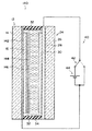
図1には本発明の第1の実施の形態に係るエレクトロクロミックミラー140の構成が概略的な断面図により示されている。
<Configuration of First Embodiment>
FIG. 1 is a schematic cross-sectional view showing the configuration of an
この図に示されるように、エレクトロクロミックミラー140は表面側基板12を備えている。表面側基板12はガラス等により形成された透明の基板本体14を備えている。この基板本体14の厚さ方向一方(図1の矢印W方向)側の面にはエレクトロクロミック膜16が形成されている。エレクトロクロミック膜16は、例えば、三酸化タングステン(WO3)や三酸化タングステン(MoO3)、又は、このような酸化物が含まれる混合物により形成されており、特に、本実施の形態では、三酸化タングステンによりエレクトロクロミック膜16が形成されている。
As shown in this figure, the
基板本体14の厚さ方向に沿ったエレクトロクロミック膜16の厚さは300nm以上1000nm以下の範囲で設定され、特に、本実施の形態ではエレクトロクロミック膜16の厚さは500nmに設定されている。また、基板本体14とエレクトロクロミック膜16との間に透明の透明電極膜142が設けられている。透明電極膜142は、インジウムチンオキサイド(In2O3:Sn、所謂「ITO」)や酸化スズ(SnO2)、フッ素ドープ酸化スズ(SnO2:F)、酸化亜鉛(ZnO2)等、更にはこれらの混合物により形成されている。この透明電極膜142にはスイッチ42を介して直流電源44の負極に接続されている。
The thickness of the
一方、エレクトロクロミック膜16の透明電極膜142とは反対側の面には透明のリチウムイオン透過膜144が形成されている。リチウムイオン透過膜144はフッ化リチウムやフッ化マグネシウムにより形成されており、スイッチ42がON状態になった場合には、電解液34のリチウムイオン(Li+)が透過する。さらに、リチウムイオン透過膜144のエレクトロクロミック膜16とは反対側の面には、銀や銀を含む合金により構成された光反射膜146が形成されている。
On the other hand, a transparent lithium ion
以上の構成の表面側基板12の厚さ方向一方の側には裏面側基板24が表面側基板12と対向するように設けられている。裏面側基板24はガラス等により形成された透明の基板本体26を備えている。この基板本体26の厚さ方向他方、すなわち、表面側基板12の側の面には導電性膜28が形成されている。導電性膜28は、クロム(Cr)やニッケル(Ni)等の金属や、インジウムチンオキサイド(In2O3:Sn、所謂「ITO」)や酸化スズ(SnO2)、フッ素ドープ酸化スズ(SnO2:F)、酸化亜鉛(ZnO2)等、更にはこれらの混合物により形成されている。
The
この導電性膜28の表面側基板12の側の面には導電性を有するカーボン膜30が形成されている。カーボン膜30はフェノール樹脂やポリイミド樹脂、又はアクリル等の合成樹脂材をバイダとして有している。また、これらのバインダの他にカーボン膜30はグラファイト、カーボンブラック、及び活性炭の混合物により形成されており、特に、この混合物には活性炭が50重量パーセント以上含まれている。
A
基板本体26の厚さ方向に沿ったカーボン膜30の厚さ寸法は50μm以上とされており、以上の構成のカーボン膜30は静電容量が10mF/cm2以上又は電荷蓄積容量が1.5Vの電圧で15mQ/cm2以上に設定され、特に本実施の形態では、静電容量が20mF/cm2又は電荷蓄積容量が1.5Vの電圧で30mQ/cm2に設定されている。
The thickness dimension of the
以上の構成の表面側基板12と裏面側基板24との間には所定の隙間が形成されていると共に、表面側基板12の外周部と裏面側基板24の外周部との間は封止材32により封止されている。表面側基板12、裏面側基板24、及び封止材32により囲まれた空間内には電解液34が封入されている。電解液34は、炭酸プロピレン、プロピレンカーボネート、エチレンカーボネート、ブチレンカーボネート、ジエチルカーボネート、γブチロラクトン、ジメチルフォルムアミド等、又はこれらの混合物により形成された溶媒を有しており、特に、本実施の形態では炭酸プロピレンが溶媒として用いられている。
A predetermined gap is formed between the front
このような溶媒の他に、電解液34は、過塩素酸リチウム(LiClO4)、六フッ化リン酸リチウム(LiPF6)、四フッ化ホウ酸リチウム(LiBF4)、リチウムビス(トリフルオロメタンスルホニル)イミド(LiN(SO2CF3)2)、リチウムビス(ペンタフルオロエタンスルホニル)イミド(LiN(SO2C2F5)2)、トリフルオロメタンスルホン酸リチウム(LiCF3SO3)等やこれらの混合物を電解質として有しており、特に、本実施の形態では過塩素酸リチウムが電解質として用いられている。
In addition to such a solvent, the
さらに、以上の構成のエレクトロクロミックミラー140の導電性膜28は、回路40を構成するスイッチ42に接続されている。スイッチ42は、ON状態で接続される端子に車両に搭載されるバッテリー等で構成され定格電圧が1.3V程度の直流電源44の正極が接続されている。この直流電源44の負極は透明電極膜142に接続されている。また、スイッチ42がOFF状態で接続される端子は、上記の直流電源44を介さずに透明電極膜142に接続されており、OFF状態では導電性膜28と透明電極膜142とが短絡される。
Further, the
<第1の実施の形態の作用、効果>
以上の構成のエレクトロクロミックミラー140では、スイッチ42のOFF状態では、透明電極膜142、エレクトロクロミック膜16、リチウムイオン透過膜144が略透明となっており、このため、基板本体14のエレクトロクロミック膜16とは反対側から入射した光は、基板本体14、透明電極膜142、エレクトロクロミック膜16、リチウムイオン透過膜144を透過して光反射膜146にて反射される。さらに、光反射膜146にて反射された光はリチウムイオン透過膜144、エレクトロクロミック膜16、透明電極膜142、及び基板本体14を透過する。
<Operation and Effect of First Embodiment>
In the
一方、スイッチ42をON状態に切り替えると、回路40を透明電極膜142の側に移動した電子(e−)がエレクトロクロミック膜16に侵入すると共に、電解液34の電解質を構成するリチウムイオン(Li+)が光反射膜146及びリチウムイオン透過膜144を透過してエレクトロクロミック膜16に侵入する。これにより、エレクトロクロミック膜16では以下の式1の還元反応が生じ、所謂タングステンブロンズと称される青色のLixWO3がエレクトロクロミック膜16で形成される。
On the other hand, when the
Li++e−+WO3→LixWO3・・・(式1)
このようにしてエレクトロクロミック膜16が青色に着色されることでエレクトロクロミック膜16が着色される前に比べて反射率が低下する。
Li + + e − + WO 3 → Li x WO 3 (Formula 1)
In this way, the
さらに、以上の還元反応が生じる際には、カーボン膜30を構成する炭素から直流電源44の側へ電子(e−)が移動し、これにより、電解質を構成する過塩素酸リチウムの負イオン(ClO4 −)がカーボン膜30の側へ移動する。これにより、上記の還元反応に対する以下の式2のような補償反応が生じる。
Furthermore, when the above reduction reaction occurs, electrons (e − ) move from the carbon constituting the
ClO4 −+C−e−→C+・ClO4 −・・・(式2)
ここで、図2には、LixWO3におけるXと、光の反射率との関係がグラフにより示されている。なお、このグラフにおいては、X=0、すなわち、三酸化タングステンが透明の場合を1として規格化されている。このグラフに示されるように、反射率はX=0.15以上で概ね飽和し、したがって、X=0.15〜0.2程度でエレクトロクロミック膜16に充分な着色が成される。
ClO 4 − + C−e − → C + · ClO 4 − (Formula 2)
Here, in FIG. 2, the relationship between X in Li x WO 3 and the reflectance of light is shown by a graph. In this graph, X = 0, that is, the case where tungsten trioxide is transparent is standardized as 1. As shown in this graph, the reflectance is almost saturated when X = 0.15 or more, and therefore, the
一方、図3にはエレクトロクロミック膜16の膜厚と反射率との関係がグラフにより示されている。なお、このグラフにおいては、エレクトロクロミック膜16がないときの反射率を1として規格化されている。このグラフに示されるように、反射率はエレクトロクロミック膜16の膜厚が300nmまでで急激に低下し、500nmで飽和するため、エレクトロクロミック膜16の膜厚は300nm以上500nm以下の範囲に設定されることが好ましい。
On the other hand, FIG. 3 is a graph showing the relationship between the thickness of the
ここで、LixWO3のXの値をX=0.15、エレクトロクロミック膜16の膜厚をd=500nm、エレクトロクロミック膜16を構成する三酸化タングステンのバルク密度をρ=7.18g/cm3、エレクトロクロミック膜16を構成する三酸化タングステンの空孔度をP=0.8、ファラデー定数をF=96485.3415Q/mol、三酸化タングステンの分子量をM=231.9molとして以下の式3に代入すると電荷蓄積容量Q=17.92mQ/cm2となり、更に、印加電圧をV=1.3として、式3の結果(すなわち、Q=17.92mQ/cm2)を以下の式4に代入すると、静電容量C=13.79mF/cm2となる。
Here, the value of X of Li x WO 3 is X = 0.15, the film thickness of the
Q=(X・d・ρ・P・F)/M・・・(式3)
C=Q/V・・・(式4)
すなわち、エレクトロクロミック膜16において充分に着色されるための還元反応には、上記の式3で求められる電荷蓄積容量、及び、式4で求められる静電容量が必要になる。ここで、本実施の形態では、カーボン膜30は活性炭を含めて構成されている。活性炭は多孔質であるが故に表面積が大きい。このため、多くの負イオン及び正電荷の蓄積能力を有しており、これにより、カーボン膜30の静電容量を20mF/cm2又は電荷蓄積容量を1.5Vの電圧で30mQ/cm2に設定できる。
Q = (X · d · ρ · P · F) / M (Formula 3)
C = Q / V (Formula 4)
In other words, the reduction reaction for sufficiently coloring the
このように、本実施の形態では、静電容量及び電荷蓄積容量共に上記の式3及び式4での計算結果よりも充分に大きい。このため、エレクトロクロミック膜16において充分な還元反応を生じさせることができ、この結果、上記のように、スイッチ42をON状態として電圧を印加することでエレクトロクロミック膜16を充分に着色できる。
As described above, in the present embodiment, both the electrostatic capacity and the charge storage capacity are sufficiently larger than the calculation results in the above formulas 3 and 4. Therefore, a sufficient reduction reaction can be caused in the
また、カーボン膜30には、活性炭のみならず、グラファイトとカーボンインクが含まれており、これにより、カーボン膜30は充分な導電性が付与され、カーボン膜30における反応を早くできる。
Further, the
さらに、本実施の形態では、エレクトロクロミック膜16を着色するに際して印加する電圧を1.3Vと低くできる。このため、スイッチ42をOFF状態にして透明電極膜142と導電性膜28とを短絡させると上記の式1及び式2とは逆向きの反応が生じ、エレクトロクロミック膜16が素早く消色される。
Furthermore, in this embodiment, the voltage applied when coloring the
ここで、本実施の形態では、光反射膜146が銀又は銀を含む合金により形成される。三酸化タングステンにより形成されたエレクトロクロミック膜16に直接銀又は銀を含む合金により形成された光反射膜146を形成すると、光反射膜146の銀がエレクトロクロミック膜16の三酸化タングステンに拡散し、三酸化タングステンが黄変する可能性がある。
Here, in this embodiment, the
しかしながら、本実施の形態では、エレクトロクロミック膜16と光反射膜146との間にリチウムイオン透過膜144を設けているため、エレクトロクロミック膜16への銀の拡散が防止又は効果的に抑制される。これにより、銀又は銀を含む合金により光反射膜146を形成しても、エレクトロクロミック膜16の黄変を防止又は効果的に抑制でき、長期に亘り品質を良好に保つことができる。
However, in this embodiment, since the lithium ion
以上のようなエレクトロクロミックミラー140を、例えば、車両における後方確認用のインナミラー(ルームミラー)やアウタミラー(ドアミラーやフェンダーミラー)等のミラー本体に用いると、昼間時にはスイッチ42をOFF状態で維持して高い反射率で後方を確認でき、夜間時等に後方の車両がヘッドライトを点灯させている場合には、スイッチ42をON状態に切り換えてエレクトロクロミック膜16を着色し、反射率を低下させることで、ヘッドライトの反射光を低減でき、眩しさが低下する。
When the
<第2の実施の形態の構成>
次に、本発明のその他の実施の形態について説明する。なお、以下の各実施の形態を説明するにあたり、前記第1の実施の形態を含めて説明している実施の形態よりも前出の実施の形態と基本的に同一の部位に関しては、同一の符号を付与してその詳細な説明を省略する。
<Configuration of Second Embodiment>
Next, other embodiments of the present invention will be described. In describing each of the following embodiments, the same parts as those in the previous embodiment are basically the same as those in the embodiment described above including the first embodiment. Reference numerals are assigned and detailed description thereof is omitted.
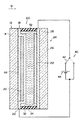
図4には本実施の形態に係るエレクトロクロミックミラー160の構成が概略的な断面図により示されている。
FIG. 4 shows a schematic cross-sectional view of the configuration of the
この図に示されるように、エレクトロクロミックミラー160は基本的に前記第5の実施の形態に係るエレクトロクロミックミラー140と同じ構成であるが、エレクトロクロミックミラー160は光反射膜146を備えておらず、代わりに光反射膜166を備えている。光反射膜166は銀や銀を含む合金により構成されている点で光反射膜146と同じであるが、外周縁が透明電極膜142の外周縁に接触し、電気的に導通している。
As shown in this figure, the
<第2の実施の形態の作用、効果>
以上の構成のエレクトロクロミックミラー160では、銀や銀を含む合金により形成された光反射膜166の外周縁が透明電極膜142の外周縁に接触し、電気的に接続されているため、スイッチ42をON状態に切り替えた際には光反射膜166を電極として機能させることができる。
<Operation and Effect of Second Embodiment>
In the
なお、本実施の形態は、光反射膜146に変えて光反射膜166を設けた点以外は基本的に前記第1の実施の形態と同じ構成であるため、前記第1の実施の形態と同様の作用を奏し、同様の効果を得ることができる。
The present embodiment is basically the same as the first embodiment except that a
<第3の実施の形態の構成>
次に、本発明の第3の実施の形態ついて説明する。
<Configuration of Third Embodiment>
Next, a third embodiment of the present invention will be described.
図5には本実施の形態に係るエレクトロクロミックミラー210の構成が概略的な断面図により示されている。
FIG. 5 is a schematic cross-sectional view showing the configuration of the
この図に示されるように、エレクトロクロミックミラー210はカーボン膜30を備えておらず、代わりに還元反応補償手段としての負イオン反応膜212が形成されている。負イオン反応膜212はポリピロール、ポリアニリン、ポリアセチレン、ポリチオフェン、ポリパラピレン、ポリフラン等の導電性ポリマ、又は、ポリビニルフェロセン等のレドックスポリマにより形成されている。例えば、ポリピロールを負イオン反応膜212として用いる場合には、ピロールを溶媒に溶かして基板本体26に塗布することで形成される。また、ポリビニルフェロセンを負イオン反応膜212として用いる場合には、ビニルフェロセンを溶媒に溶かして基板本体26に塗布することで形成される。この負イオン反応膜212の質量は0.012mg/cm2以上となるように設定されている。
As shown in this figure, the
<第3の実施の形態の作用、効果>
本エレクトロクロミックミラー210では、スイッチ42をON状態に切り替えることで、上記式1の還元反応がエレクトロクロミック膜16で生じる際には、負イオン反応膜212を構成する導電性ポリマ又はレドックスポリマが酸化されて正の電荷を帯びる。これにより、電解質を構成する過塩素酸リチウムの負イオン(ClO4 −)が負イオン反応膜212に侵入して電荷バランスをとる。このように、上記の還元反応に対して、負イオン反応膜212がポリピロールにより形成されていれば以下の式5aのような補償反応が生じ、負イオン反応膜212がポリビニルフェロセンにより形成されていれば以下の式5bのような補償反応が生じ、
ClO4 −+PPy−e−→PPy+・ClO4 −・・・(式5a)
ClO4 −+PVF−e−→PVF+・ClO4 −・・・(式5b)
なお、式5aにおいてPPyはポリピロールを指し、式5aにおいてPVFはポリビニルフェロセンを指す。
<Operation and Effect of Third Embodiment>
In this
ClO 4 − + PPy−e − → PPy + · ClO 4 − (Formula 5a)
ClO 4 − + PVF−e − → PVF + · ClO 4 − (Formula 5b)
In Formula 5a, PPy refers to polypyrrole, and in Formula 5a, PVF refers to polyvinyl ferrocene.
ここで、LixWO3のXの値をX=0.15、エレクトロクロミック膜16の膜厚をd=500nm、エレクトロクロミック膜16を構成する三酸化タングステンのバルク密度をρ=7.18g/cm3、エレクトロクロミック膜16を構成する三酸化タングステンの空孔度をP=0.8、三酸化タングステンの分子量をMW=231.9molとして以下の式6に代入すると、三酸化タングステンの反応量(モル数)n=1.86mM/cm2となる。
Here, the value of X of Li x WO 3 is X = 0.15, the film thickness of the
n=(X・d・ρ・P)/MW・・・(式6)
さらに、負イオン反応膜212を構成する導電性ポリマ又はレドックスポリマも上記のnと同じモル数だけ反応しなくてはならない。したがって、負イオン反応膜212に用いられる導電性ポリマ又はレドックスポリマのモノマー当たりの分子量をMP=65.07g/molとして以下の式7に代入すると、m=0.012mg/cm2の質量の導電性ポリマ又はレドックスポリマが必要になる。
n = (X · d · ρ · P) / M W ··· ( Equation 6)
Furthermore, the conductive polymer or redox polymer constituting the negative
m=n・MP・・・(式7)
ここで、本実施の形態では、負イオン反応膜212はm=0.012mg/cm2以上に設定されている。このため、エレクトロクロミック膜16において充分な還元反応を生じさせることができ、この結果、上記のように、スイッチ42をON状態として電圧を印加することでエレクトロクロミック膜16を充分に着色できる。
m = n · M P ··· (Equation 7)
Here, in the present embodiment, the negative
さらに、本実施の形態では、エレクトロクロミック膜16を着色するに際して印加する電圧を1.3Vと低くできる。このため、スイッチ42をOFF状態にして透明電極膜142と導電性膜28とを短絡させると上記の式1、式5a又は式5bとは逆向きの反応が生じ、エレクトロクロミック膜16が素早く消色される。
Furthermore, in this embodiment, the voltage applied when coloring the
以上のようなエレクトロクロミックミラー210を、例えば、車両における後方確認用のインナミラー(ルームミラー)やアウタミラー(ドアミラーやフェンダーミラー)等のミラー本体に用いると、昼間時にはスイッチ42をOFF状態で維持して高い反射率で後方を確認でき、夜間時等に後方の車両がヘッドライトを点灯させている場合には、スイッチ42をON状態に切り換えてエレクトロクロミック膜16を着色し、反射率を低下させることで、ヘッドライトの反射光を低減でき、眩しさが低下する。
When the
<第4の実施の形態の構成>
図6には本発明の第4の実施の形態に係るエレクトロクロミックミラー220の構成が概略的な断面図により示されている。
<Configuration of Fourth Embodiment>
FIG. 6 is a schematic cross-sectional view showing the configuration of an
この図に示されるように、エレクトロクロミックミラー220では導電性膜28が銀(Ag)により形成されている。この導電性膜28の表面側基板12の側の面にはカーボン膜30が形成されておらず、代わりに析出膜として還元反応補償手段を構成する難溶性塩膜224が形成されている。難溶性塩膜224は塩化銀、塩化臭素、塩化チオシアン酸等により形成されており、特に、本実施の形態では難溶性塩膜224が塩化銀により形成されている。
As shown in this figure, in the
<第4の実施の形態の作用、効果>
本エレクトロクロミックミラー220では、スイッチ42をON状態に切り替えることで、上記式1の還元反応がエレクトロクロミック膜16で生じる際には、以下の式8に示されるように、導電性膜28を形成する銀(Ag)に電解質を構成する過塩素酸リチウムの負イオン(Cl−)が反応し、これにより、塩化銀(AgCl)が生成され、塩化銀により形成された難溶性塩膜224上に析出される。これにより、上記の還元反応に応じた補償がなされる。
<Operation and Effect of Fourth Embodiment>
In the
Cl−+Ag−e−→AgCl・・・(式8)
このように、本実施の形態では、エレクトロクロミック膜16における還元反応に対して保障反応が確実に生じるので、エレクトロクロミック膜16を着色するに際して印加する電圧を1.3Vと低くできる。このため、スイッチ42をOFF状態にして透明電極膜142と導電性膜28とを短絡させると上記の式1及び式8とは逆向きの反応が生じ、エレクトロクロミック膜16が素早く消色される。
Cl − + Ag−e − → AgCl (formula 8)
As described above, in the present embodiment, since a guarantee reaction is surely generated with respect to the reduction reaction in the
以上のようなエレクトロクロミックミラー220を、例えば、車両における後方確認用のインナミラー(ルームミラー)やアウタミラー(ドアミラーやフェンダーミラー)等のミラー本体に用いると、昼間時にスイッチ42をOFF状態で維持して高い反射率で後方を確認でき、夜間時等に後方の車両がヘッドライトを点灯させている場合には、スイッチ42をON状態に切り換えてエレクトロクロミック膜16を着色し、反射率を低下させることで、ヘッドライトの反射光を低減でき、眩しさが低下する。
When the
<第5の実施の形態の構成>
図7には本発明の第5の実施の形態に係るエレクトロクロミックミラー240の構成が概略的な断面図により示されている。
<Configuration of Fifth Embodiment>
FIG. 7 is a schematic cross-sectional view showing the configuration of an
この図に示されるように、エレクトロクロミックミラー240では導電性膜28の表面側基板12の側の面にはカーボン膜30が形成されていない。また、電解液34に代わり電解液244が表面側基板12と裏面側基板24との間に封入されている。
As shown in this figure, in the
電解液244には、電解液34を構成する材質の他に、還元反応補償手段を構成する酸化剤としての中性物質であるフェロセン(Fe(C5H5)2)が含まれている。
In addition to the material constituting the
<第5の実施の形態の作用、効果>
本エレクトロクロミックミラー240では、スイッチ42をON状態に切り替えることで、上記式1の還元反応がエレクトロクロミック膜16で生じる際には、以下の式9に示されるように、電解液244に含まれるフェロセンが正の電荷を帯びる。これにより、上記の還元反応に応じた補償がなされる。
<Operation and Effect of Fifth Embodiment>
In the
Fe(C5H5)2→〔Fe(C5H5)2〕+・・・(式9)
このように、本実施の形態では、エレクトロクロミック膜16における還元反応に対して保障反応が確実に生じるので、エレクトロクロミック膜16を着色するに際して印加する電圧を1.3Vと低くできる。このため、スイッチ42をOFF状態にして透明電極膜142と導電性膜28とを短絡させると上記の式1及び式9とは逆向きの反応が生じ、エレクトロクロミック膜16が素早く消色される。
Fe (C 5 H 5 ) 2 → [Fe (C 5 H 5 ) 2 ] + (Formula 9)
As described above, in the present embodiment, since a guarantee reaction is surely generated with respect to the reduction reaction in the
以上のようなエレクトロクロミックミラー240を、例えば、車両における後方確認用のインナミラー(ルームミラー)やアウタミラー(ドアミラーやフェンダーミラー)等のミラー本体に用いると、昼間時にスイッチ42をOFF状態で維持して高い反射率で後方を確認でき、夜間時等に後方の車両がヘッドライトを点灯させている場合には、スイッチ42をON状態に切り換えてエレクトロクロミック膜16を着色し、反射率を低下させることで、ヘッドライトの反射光を低減でき、眩しさが低下する。
When the
なお、上記の第3の実施の形態から第5の実施の形態は、第1の実施の形態の変形例であったが、第3の実施の形態から第5の実施の形態を第2の実施の形態の変形例とする構成としてもよい。 The third to fifth embodiments described above are modifications of the first embodiment. However, the third to fifth embodiments are different from the third embodiment. It is good also as a structure made into the modification of embodiment.
140 エレクトロクロミックミラー
16 エレクトロクロミック膜
28 導電性膜
30 カーボン膜(還元反応補償手段)
34 電解液
142 透明電極膜
144 リチウムイオン透過膜
146 光反射膜
160 エレクトロクロミックミラー
166 光反射膜
210 エレクトロクロミックミラー
212 負イオン反応膜(還元反応補償手段)
220 エレクトロクロミックミラー
224 難溶性塩膜(析出膜、還元反応補償手段)
240 エレクトロクロミックミラー
244 電解液(還元反応補償手段)
140
34
220
240
Claims (7)
前記透明電極膜の厚さ方向一方の側に形成されて還元反応することで着色されるエレクトロクロミック膜と、
銀又は銀を含む合金により形成されて前記透明電極膜及び前記エレクトロクロミック膜を透過した光を反射する光反射膜と、
前記エレクトロクロミック膜と前記光反射膜との間に設けられ、前記リチウムイオンを透過すると共に前記光反射膜の側から前記エレクトロクロミック膜の側への銀の拡散を規制する透明のリチウムイオン透過膜と、
前記透明電極膜の厚さ方向一方の側で前記光反射膜の前記リチウムイオン透過膜とは反対側に設けられた導電性を有する導電性膜と、
リチウムイオンを含めて構成されて前記光反射膜と前記導電性膜との間に封入され、前記導電性膜を正とし前記透明電極膜を負として電圧を印加することで前記リチウムイオンが前記エレクトロクロミック膜の側へ移動して、前記エレクトロクロミック膜の還元反応に供される電解液と、
を備えるエレクトロクロミックミラー。 A transparent electrode film capable of transmitting light and having conductivity;
An electrochromic film formed on one side in the thickness direction of the transparent electrode film and colored by a reduction reaction;
A light reflecting film that reflects light that is formed of silver or an alloy containing silver and that has passed through the transparent electrode film and the electrochromic film;
A transparent lithium ion permeable film that is provided between the electrochromic film and the light reflecting film and transmits the lithium ions and restricts diffusion of silver from the light reflecting film side to the electrochromic film side. When,
A conductive film having conductivity provided on one side of the transparent electrode film in the thickness direction opposite to the lithium ion permeable film of the light reflecting film;
Lithium ions are contained and sealed between the light reflecting film and the conductive film, and the lithium ions are converted into the electrosphere by applying a voltage with the conductive film being positive and the transparent electrode film being negative. An electrolyte solution that moves to the chromic film side and is subjected to a reduction reaction of the electrochromic film;
Electrochromic mirror equipped with.
ことを特徴とする請求項3に記載のエレクトロクロミックミラー。 The reduction compensation means is configured including a carbon film formed including activated carbon and provided on the light reflecting film side of the conductive film.
The electrochromic mirror according to claim 3.
ことを特徴とする請求項3に記載のエレクトロクロミックミラー。 It is formed of a conductive polymer or a redox polymer, is provided on the side of the light reflecting film of the conductive film, and is oxidized by negative ions moved to the side of the conductive film when the voltage is applied. Constructing the reduction compensation means including a negative ion reaction membrane,
The electrochromic mirror according to claim 3.
ことを特徴とする請求項3に記載のエレクトロクロミックミラー。 The conductive film is formed of silver or an alloy containing silver, and the conductive film is formed when a voltage is applied with the conductive film being positive and the first and second conductive reflective films being negative. The electrolyte is formed including negative ions of a hardly soluble salt that reacts with ions of the salt, and further, formed of a hardly soluble salt, provided on the light reflecting film side of the conductive film, and applied with the voltage. And providing a deposited film for depositing a precipitate formed by a reaction between the negative ions of the hardly soluble salt moved to the conductive film side and the silver ions constituting the conductive film. The reduction reaction compensation means was configured including silver forming a conductive film, negative ions constituting the electrolytic solution, and the deposited film.
The electrochromic mirror according to claim 3.
ことを特徴とする請求項3に記載のエレクトロクロミックミラー。 The electrolytic solution is configured to include a reactive material that can be oxidized by neutral molecules or negative ions and can be oxidized by applying a voltage with the conductive film being positive and the first and second conductive reflective films being negative. The reduction reaction compensation means including the reaction material is configured.
The electrochromic mirror according to claim 3.
Priority Applications (4)
| Application Number | Priority Date | Filing Date | Title |
|---|---|---|---|
| JP2007167914A JP2009008751A (en) | 2007-06-26 | 2007-06-26 | Electrochromic mirror |
| US12/144,151 US7643201B2 (en) | 2007-06-26 | 2008-06-23 | Electrochromic mirror |
| EP08011369A EP2009491A1 (en) | 2007-06-26 | 2008-06-23 | Electrochromic mirror |
| CNA2008101249891A CN101334566A (en) | 2007-06-26 | 2008-06-25 | Electrochromic mirror |
Applications Claiming Priority (1)
| Application Number | Priority Date | Filing Date | Title |
|---|---|---|---|
| JP2007167914A JP2009008751A (en) | 2007-06-26 | 2007-06-26 | Electrochromic mirror |
Publications (1)
| Publication Number | Publication Date |
|---|---|
| JP2009008751A true JP2009008751A (en) | 2009-01-15 |
Family
ID=39673236
Family Applications (1)
| Application Number | Title | Priority Date | Filing Date |
|---|---|---|---|
| JP2007167914A Pending JP2009008751A (en) | 2007-06-26 | 2007-06-26 | Electrochromic mirror |
Country Status (4)
| Country | Link |
|---|---|
| US (1) | US7643201B2 (en) |
| EP (1) | EP2009491A1 (en) |
| JP (1) | JP2009008751A (en) |
| CN (1) | CN101334566A (en) |
Cited By (1)
| Publication number | Priority date | Publication date | Assignee | Title |
|---|---|---|---|---|
| JP2011095503A (en) * | 2009-10-29 | 2011-05-12 | Tokai Rika Co Ltd | Electrochromic mirror |
Families Citing this family (13)
| Publication number | Priority date | Publication date | Assignee | Title |
|---|---|---|---|---|
| US7800807B2 (en) * | 2007-06-26 | 2010-09-21 | Kabushiki Kaisha Tokai-Rika-Denki-Seisakusho | Electrochromic mirror |
| JP4972001B2 (en) * | 2008-01-23 | 2012-07-11 | 株式会社東海理化電機製作所 | Electrochromic mirror |
| US9752932B2 (en) | 2010-03-10 | 2017-09-05 | Drexel University | Tunable electro-optic filter stack |
| US9576694B2 (en) | 2010-09-17 | 2017-02-21 | Drexel University | Applications for alliform carbon |
| CN102955263A (en) * | 2012-11-29 | 2013-03-06 | 中山市创科科研技术服务有限公司 | Sunglasses capable of simultaneously adjusting light transmittance and color |
| CN104298043A (en) * | 2014-10-22 | 2015-01-21 | 京东方科技集团股份有限公司 | Electrochromic display device and unit |
| CN104788022B (en) * | 2015-03-31 | 2017-04-05 | 哈尔滨工业大学 | The application of flake nano silver electrochomeric films |
| CN105644449B (en) * | 2016-01-11 | 2018-01-30 | 深圳市华星光电技术有限公司 | Antiglaring rear mirror |
| JP6665210B2 (en) * | 2016-02-15 | 2020-03-13 | シャープ株式会社 | Electrochromic device and smart window with electrochromic device |
| CN106773440A (en) * | 2017-03-13 | 2017-05-31 | 信利光电股份有限公司 | A kind of anti-glare lens making process and vehicle |
| CN107085316A (en) | 2017-06-30 | 2017-08-22 | 京东方科技集团股份有限公司 | Liquid crystal lens and liquid crystal glasses |
| CN111061108B (en) * | 2019-11-25 | 2021-08-13 | 中国科学技术大学 | Electrochromic glass based on molybdenum trioxide thin film, and preparation method and application thereof |
| CN113156730B (en) * | 2020-01-23 | 2022-07-19 | 青岛凯欧斯光电科技有限公司 | Method for controlling electrochromic device |
Citations (10)
| Publication number | Priority date | Publication date | Assignee | Title |
|---|---|---|---|---|
| JPS5844424A (en) * | 1972-12-13 | 1983-03-15 | アメリカン・サイアナミツド・カンパニー | Radiant rays reflecting apparatus |
| JPS6153736U (en) * | 1984-09-14 | 1986-04-11 | ||
| JPS6156640U (en) * | 1984-09-17 | 1986-04-16 | ||
| JPS61210388A (en) * | 1985-03-15 | 1986-09-18 | 日立マクセル株式会社 | Electrochromic display element |
| JPS63271321A (en) * | 1987-04-30 | 1988-11-09 | Hidetoshi Tsuchida | Fully solid-state high-polymer type electrochromic display element |
| JPH04328723A (en) * | 1991-04-30 | 1992-11-17 | Tonen Corp | Electrochromic element |
| JPH05313211A (en) * | 1992-05-13 | 1993-11-26 | Tajima Inc | Electrochromic element |
| JP2003161963A (en) * | 2001-11-29 | 2003-06-06 | Nippon Oil Corp | Electrochromic element |
| JP2005031628A (en) * | 2003-06-18 | 2005-02-03 | Tokai Rika Co Ltd | Electrochromic mirror |
| JP2006235632A (en) * | 2005-02-23 | 2006-09-07 | Sage Electrochromics Inc | Electrochromic device and its manufacturing method |
Family Cites Families (5)
| Publication number | Priority date | Publication date | Assignee | Title |
|---|---|---|---|---|
| US5138481A (en) * | 1991-07-23 | 1992-08-11 | Ford Motor Company | Electrochromic device with color gradient and method of making the device |
| JPH10239716A (en) * | 1996-12-24 | 1998-09-11 | Nippon Oil Co Ltd | Counter electrode for electrochromic element, and electrochromic element |
| US6700692B2 (en) * | 1997-04-02 | 2004-03-02 | Gentex Corporation | Electrochromic rearview mirror assembly incorporating a display/signal light |
| JP2005309137A (en) * | 2004-04-22 | 2005-11-04 | Tokai Rika Co Ltd | Reflectivity variable mirror |
| JP4544903B2 (en) * | 2004-04-26 | 2010-09-15 | 株式会社東海理化電機製作所 | Electrochromic mirror |
-
2007
- 2007-06-26 JP JP2007167914A patent/JP2009008751A/en active Pending
-
2008
- 2008-06-23 US US12/144,151 patent/US7643201B2/en not_active Expired - Fee Related
- 2008-06-23 EP EP08011369A patent/EP2009491A1/en not_active Withdrawn
- 2008-06-25 CN CNA2008101249891A patent/CN101334566A/en active Pending
Patent Citations (10)
| Publication number | Priority date | Publication date | Assignee | Title |
|---|---|---|---|---|
| JPS5844424A (en) * | 1972-12-13 | 1983-03-15 | アメリカン・サイアナミツド・カンパニー | Radiant rays reflecting apparatus |
| JPS6153736U (en) * | 1984-09-14 | 1986-04-11 | ||
| JPS6156640U (en) * | 1984-09-17 | 1986-04-16 | ||
| JPS61210388A (en) * | 1985-03-15 | 1986-09-18 | 日立マクセル株式会社 | Electrochromic display element |
| JPS63271321A (en) * | 1987-04-30 | 1988-11-09 | Hidetoshi Tsuchida | Fully solid-state high-polymer type electrochromic display element |
| JPH04328723A (en) * | 1991-04-30 | 1992-11-17 | Tonen Corp | Electrochromic element |
| JPH05313211A (en) * | 1992-05-13 | 1993-11-26 | Tajima Inc | Electrochromic element |
| JP2003161963A (en) * | 2001-11-29 | 2003-06-06 | Nippon Oil Corp | Electrochromic element |
| JP2005031628A (en) * | 2003-06-18 | 2005-02-03 | Tokai Rika Co Ltd | Electrochromic mirror |
| JP2006235632A (en) * | 2005-02-23 | 2006-09-07 | Sage Electrochromics Inc | Electrochromic device and its manufacturing method |
Cited By (1)
| Publication number | Priority date | Publication date | Assignee | Title |
|---|---|---|---|---|
| JP2011095503A (en) * | 2009-10-29 | 2011-05-12 | Tokai Rika Co Ltd | Electrochromic mirror |
Also Published As
| Publication number | Publication date |
|---|---|
| EP2009491A1 (en) | 2008-12-31 |
| US7643201B2 (en) | 2010-01-05 |
| CN101334566A (en) | 2008-12-31 |
| US20090002801A1 (en) | 2009-01-01 |
Similar Documents
| Publication | Publication Date | Title |
|---|---|---|
| JP2009008751A (en) | Electrochromic mirror | |
| US11780777B2 (en) | Electrochromic device including lithium-rich anti-perovskite material | |
| KR102010733B1 (en) | Electrochromic device | |
| KR20010033200A (en) | Electrodeposition cell with high light transmission | |
| US20100172011A1 (en) | Semi-electroactive material containing organic compounds having positive or negative redox activity, process and kit for manufacturing this material, electrically controllable device and glazing units using such a semi-electroactive material | |
| JP2010002573A (en) | Method for changing reflectivity reversibly, element therefor, method of manufacturing element, and transmittance variable element and reflectivity variable mirror | |
| EP1488957A1 (en) | Electrochromic mirror having variable reflectivity | |
| US7692843B2 (en) | Electrochromic mirror | |
| JP4949287B2 (en) | Electrochromic mirror | |
| JP5014893B2 (en) | Electrochromic mirror | |
| JPWO2009031422A1 (en) | Method for manufacturing electrochromic display element | |
| JP4972001B2 (en) | Electrochromic mirror | |
| WO2014142216A1 (en) | Electrochromic device, image pickup optical system, image pickup apparatus, and window member | |
| JP4949136B2 (en) | Electrochromic mirror | |
| US7800807B2 (en) | Electrochromic mirror | |
| JP2009008750A (en) | Electrochromic mirror | |
| JP2009008749A (en) | Electrochromic mirror | |
| JP2011141425A (en) | Electrochromic mirror | |
| JP2011141426A (en) | Electrochromic mirror | |
| JP2011095487A (en) | Electrochromic mirror | |
| JP2011095483A (en) | Electrochromic mirror | |
| JP2011095503A (en) | Electrochromic mirror | |
| JP2012150184A (en) | Electrochromic mirror |
Legal Events
| Date | Code | Title | Description |
|---|---|---|---|
| A621 | Written request for application examination |
Free format text: JAPANESE INTERMEDIATE CODE: A621 Effective date: 20100329 |
|
| A521 | Written amendment |
Free format text: JAPANESE INTERMEDIATE CODE: A821 Effective date: 20100330 Free format text: JAPANESE INTERMEDIATE CODE: A821 Effective date: 20100329 |
|
| A131 | Notification of reasons for refusal |
Free format text: JAPANESE INTERMEDIATE CODE: A131 Effective date: 20111108 |
|
| A02 | Decision of refusal |
Free format text: JAPANESE INTERMEDIATE CODE: A02 Effective date: 20120321 |