JP2009003076A - Developing device and image forming apparatus - Google Patents
Developing device and image forming apparatus Download PDFInfo
- Publication number
- JP2009003076A JP2009003076A JP2007162353A JP2007162353A JP2009003076A JP 2009003076 A JP2009003076 A JP 2009003076A JP 2007162353 A JP2007162353 A JP 2007162353A JP 2007162353 A JP2007162353 A JP 2007162353A JP 2009003076 A JP2009003076 A JP 2009003076A
- Authority
- JP
- Japan
- Prior art keywords
- developer
- carrier
- image
- magnetic
- developing device
- Prior art date
- Legal status (The legal status is an assumption and is not a legal conclusion. Google has not performed a legal analysis and makes no representation as to the accuracy of the status listed.)
- Granted
Links
Images


Abstract
Description
本発明は、像担持体上の潜像を現像する現像装置及び画像形成装置に関する。 The present invention relates to a developing device and an image forming apparatus for developing a latent image on an image carrier.
従来より、電子写真方式を用いた画像形成装置において、磁性分を含む現像剤を用いた現像装置により静電潜像を形成した像担持体表面を現像する方式が知られている。 2. Description of the Related Art Conventionally, in an image forming apparatus using an electrophotographic method, a method of developing an image carrier surface on which an electrostatic latent image is formed by a developing device using a developer containing a magnetic component is known.
このような現像装置としては、磁性トナーを用いた磁性1成分現像方式や非磁性のトナーと磁性のキャリアを用いた2成分現像方式があり、ともに内部に複数のマグネットを有する現像剤担持体を備えている。 As such a developing device, there are a magnetic one-component developing system using magnetic toner and a two-component developing system using non-magnetic toner and a magnetic carrier, both of which include a developer carrier having a plurality of magnets inside. I have.
現像剤担持体は、内蔵するマグネットによりその表面に現像剤を担持搬送するとともに規制部材により一定の層厚になるように規制している。規制部材は、一般に現像剤担持体表面との間に一定の隙間を作って配置され、その隙間を調整することにより、必要な現像剤量の層厚を現像剤担持体上に形成するように現像剤量の規制をしている。 The developer carrying member carries the developer on its surface by a built-in magnet and is regulated to have a constant layer thickness by a regulating member. The regulating member is generally arranged with a certain gap between it and the surface of the developer carrier, and by adjusting the gap, a layer thickness of the required developer amount is formed on the developer carrier. The amount of developer is regulated.
ところでこのような現像装置を長期に使用すると現像剤が劣化するという問題がある。 By the way, when such a developing device is used for a long time, there is a problem that the developer deteriorates.
現像剤劣化は、具体的には現像剤表面の変質である。例えば、2成分現像装置においては、キャリアの劣化ある。キャリア劣化の一つに、長く使用するうちにトナーに外添処理された微粒子やトナー微粒子が現像装置内に蓄積し、キャリア表面に付着する現象がある。このようなキャリア表面への異物付着によりトナーとキャリアの接触が阻害されトナーの荷電量を低下させる。またキャリアは一般的にフェライトあるいはマグネタイト等のコア材に樹脂コートされたものが使用されている。これらコート材はキャリアの抵抗調整やトナーを荷電し易くする為に処理されもので、このコート層の摩耗もキャリア劣化として、トナーの荷電量低下を来たす。現像剤劣化はキャリアの劣化だけではなく、トナーもまた劣化する。トナー表面には、流動性の向上や荷電性の調整を目的に外添処理がなされるが、使用するにつれ、離脱したり、トナー母材表面に埋没したりして、トナーの荷電量が低下する。このような現像剤の劣化の主要因が現像剤担持体上に設けられた規制部材によるもので、規制部分の現像剤に圧縮や擦れなどのストレスが加わるためであることが分かっている。 Specifically, the developer deterioration is an alteration of the developer surface. For example, in a two-component developing device, there is carrier deterioration. One of the carrier deteriorations is a phenomenon in which fine particles or toner fine particles that have been externally added to the toner over a long period of time accumulate in the developing device and adhere to the carrier surface. Such adhesion of foreign matter to the surface of the carrier obstructs contact between the toner and the carrier and reduces the charge amount of the toner. The carrier is generally a resin coated core material such as ferrite or magnetite. These coating materials are processed in order to adjust the resistance of the carrier and to make the toner easy to be charged. Wear of the coating layer also causes carrier deterioration, resulting in a decrease in the charge amount of the toner. The developer deterioration not only deteriorates the carrier but also the toner. The toner surface is externally added for the purpose of improving fluidity and adjusting the chargeability. However, as the toner is used, it is detached or buried in the surface of the toner base material, and the charge amount of the toner decreases. To do. It has been found that the main cause of the deterioration of the developer is a restriction member provided on the developer carrier, and stress such as compression or rubbing is applied to the developer in the restriction portion.
この規制部のストレスを低減することにより、現像剤劣化を抑制し、長期に安定したトナー帯電量が得られる現像装置が望まれている。 There is a demand for a developing device that can suppress the deterioration of the developer by reducing the stress of the restricting portion and obtain a stable toner charge amount over a long period of time.
特許文献1においては、規制部に磁性部材を用い、現像剤担持体と対向する磁性部材の先端面が、現像スリーブの回転方向下流側に向かって現像スリーブ表面に近づくようにすることで、該先端面と現像スリーブとの間に形成される磁気ブラシの領域を広くすることができ、現像剤に対するストレスを低減できる方法として提案されている。
しかしながら、特許文献1の方法においても、十分に耐久性のある現像装置が得られず、長期に使用することにより、現像剤劣化によって生じた帯電不良トナーによる画像カブリが発生した。
However, even with the method of
本発明は、像担持体上の潜像を現像する現像装置において、現像剤の劣化を抑制し、画像カブリがなく、長期にわたり良好な画像形成を行える現像装置および画像形成装置を提供することを目的とする。 The present invention provides a developing device that develops a latent image on an image bearing member, suppresses the deterioration of the developer, does not cause image fogging, and can perform good image formation over a long period of time, and an image forming device. Objective.
上記の課題を解決するために、本発明は以下の特徴を有するものである。 In order to solve the above problems, the present invention has the following features.
1.
内部にマグネットを有し、表面に現像剤を担持する現像剤担持体と、
前記現像剤担持体に近接配置され、該現像剤担持体の表面に担持する現像剤の層厚を規制する規制部材とを備え、
前記規制部材は、非磁性部材と、
前記非磁性部材に対して前記現像剤担持体上の現像剤搬送方向上流側及び下流側に配設された2つの磁性部材とを有し、
前記現像剤担持体と最も近接する部分が、前記非磁性部材であることを特徴とする現像装置。
1.
A developer carrying body having a magnet inside and carrying a developer on the surface;
A regulating member that is disposed close to the developer carrying member and regulates the layer thickness of the developer carried on the surface of the developer carrying member;
The regulating member is a non-magnetic member,
Two magnetic members disposed on the upstream side and the downstream side in the developer transport direction on the developer carrier relative to the non-magnetic member,
The developing device characterized in that a portion closest to the developer carrying member is the nonmagnetic member.
2.
前記非磁性部材が前記現像剤担持体の表面に対向する先端部は、前記現像剤担持体の現像剤搬送方向下流に向かって前記現像剤担持体の表面に近づく面を有することを特徴とする1に記載の現像装置。
2.
A tip portion where the non-magnetic member faces the surface of the developer carrier has a surface that approaches the surface of the developer carrier toward the downstream side of the developer carrier in the developer transport direction. 2. The developing device according to 1.
3.
前記先端部は、先端角度が鈍角となる2つの面からなることを特徴とする2に記載の現像装置。
3.
3. The developing device according to 2, wherein the tip end part is composed of two surfaces whose tip end angle is an obtuse angle.
4.
前記先端部は、凸状の曲面からなることを特徴とする2に記載の現像装置。
4).
3. The developing device according to 2, wherein the tip portion is a convex curved surface.
5.
前記非磁性部材の上流側に配設された磁性部材の前記現像剤担持体に対向する面は、前記現像剤担持体の現像剤搬送方向下流に向かって前記現像剤担持体の表面に接近する面を有することを特徴とする1乃至4の何れか1項に記載の現像装置。
5).
The surface of the magnetic member disposed on the upstream side of the non-magnetic member that faces the developer carrying member approaches the surface of the developer carrying member toward the downstream in the developer carrying direction of the developer carrying member. 5. The developing device according to any one of 1 to 4, which has a surface.
6.
像担持体と、該像担持体上に静電潜像を形成する静電潜像形成手段と、前記像担持体上の静電潜像を現像するための1乃至5の何れか1項に記載の現像装置と、を有することを特徴とする画像形成装置。
6).
6. An image carrier, an electrostatic latent image forming unit that forms an electrostatic latent image on the image carrier, and any one of 1 to 5 for developing the electrostatic latent image on the image carrier An image forming apparatus comprising: the developing device described above.
本発明によれば、現像剤担持体に近接配置され、現像剤担持体の表面に担持する現像剤の層厚を規制する規制部材が、非磁性部材と、非磁性部材に対して現像剤担持体上の現像剤搬送方向上流側及び下流側に配設された2つの磁性部材とを有し、現像剤担持体と最も近接する部分が、非磁性部材となるようにした。このようにすることで、現像剤担持体上の現像剤を規制部材で規制する時の現像剤に対するストレスを低減することができ、現像剤の劣化を抑制し、画像かぶりのない、長期に渡って安定したトナーの帯電量を実現できる。よって、良好な画像形成を行える長寿命な現像装置および画像形成装置を提供することができる。 According to the present invention, the regulating member that is disposed in proximity to the developer carrying member and regulates the layer thickness of the developer carried on the surface of the developer carrying member includes the nonmagnetic member and the developer carrying member with respect to the nonmagnetic member. And two magnetic members disposed on the upstream side and the downstream side in the developer conveying direction on the body, and the portion closest to the developer carrying member is a non-magnetic member. By doing so, it is possible to reduce stress on the developer when the developer on the developer carrying member is regulated by the regulating member, to suppress the deterioration of the developer, and to prevent image fogging for a long period of time. And stable toner charge amount. Therefore, it is possible to provide a long-life developing device and image forming apparatus capable of forming a good image.
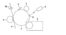
図1に本発明の画像形成装置に係る一実施形態を示す。この画像形成装置は、電子写真方式により像担持体1に形成されたトナー像を用紙等の転写媒体Pに転写して画像形成を行うプリンタである。この画像形成装置は画像を担持するための像担持体1を有しており、像担持体1の周辺には、像担持体1を帯電するための帯電手段としての帯電部材3、像担持体1上の静電潜像を現像する現像装置2、像担持体1上のトナー像を転写するための転写ローラ4、及び像担持体1上の残留トナー除去用のクリーニング部材5が、像担持体1の回転方向に沿って順に配置されている。
FIG. 1 shows an embodiment of an image forming apparatus according to the present invention. This image forming apparatus is a printer that forms an image by transferring a toner image formed on an
像担持体1は、帯電部材3で帯電された後に、図中のE点の位置でレーザ発光器などを備えた露光装置6により露光されて、その表面上に静電潜像が形成される。現像装置2は、この静電潜像をトナー像に現像する。転写ローラ4は、この像担持体1上のトナー像を転写媒体Pに転写した後、定着装置90で定着し、図中の矢印方向に排出する。クリーニング部材5は、転写後の像担持体1上の残留トナーを、その機械的な力で除去する。画像形成装置に用いられる像担持体1、帯電部材3、転写ローラ4、クリーニングブレード5、露光装置6等は、周知の電子写真方式の技術を任意に使用してよい。例えば、帯電手段として図中、帯電ローラが示されているが、像担持体1と非接触の帯電装置であってもよい。また例えば、クリーニング部材はなくてもよい。
The
次に本発明の画像形成装置に用いられる現像装置について、図2を用いてさらに詳細に説明する。本実施形態において現像装置2は、キャリアとトナーを含む2成分現像剤12を収容する現像剤槽13、該現像剤槽13から供給された現像剤を表面に担持搬送する現像剤担持体としての現像ローラ9、現像ローラ9と一定の間隔を設けて配置された規制部材11を備える。
Next, the developing device used in the image forming apparatus of the present invention will be described in more detail with reference to FIG. In the present embodiment, the developing
現像ローラ9は、内部にマグネットローラ8を内包し、その外側にφ18の円筒状のスリーブローラ7をマグネットローラ8とは独立に回転可能に備えている。マグネットローラ8は、周面に5極(N1、S1、N2、S2、N3)の磁極を有し、固定されており、スリーブローラ7は、アルミニウムなどの非磁性材料からなる。
The developing
現像剤槽13の現像剤12は、攪拌部材14、15により攪拌され、規制部材11の方に搬送される。搬送された現像剤12は、現像ローラ9の磁極N1に引きつけられ現像ローラ9の表面に吸着される。
The
マグネットローラ8の5つの磁極のうち、主磁極S2は、像担持体1と対向する位置に配されており、また、スリーブローラ7上の現像剤を剥離するための反発磁界を発生させる同極部N1,N3は、現像剤槽13の現像剤槽13側に対向する位置に配置されている。
Of the five magnetic poles of the
磁極N1によりスリーブローラ7の表面に吸着した現像剤は、スリーブローラ7の表面と所定のギャップを形成した規制部材11により、現像剤の通過を規制して現像剤の量を調整する。N1に対向するスリーブローラ7の表面の法線方向の磁束密度は、適宜決めることができるが、本実施形態では、50mTとした。
The developer adsorbed on the surface of the
また、像担持体1の周速及びスリーブローラ7の周速も適宜決めて良いが、本実施形態では、像担持体の周速を100mm/sとし、スリーブローラ7の周速を150mm/sとした。
Further, the peripheral speed of the
図3を用いて、規制部材11について説明する。規制部材11は、現像ローラ9に内包されたマグネットローラ8の磁極N1に対向し、スリーブローラ7と所定の距離dを介して配置されている。規制部材11は、非磁性部材113と、この非磁性部材113に対して、現像ローラ9上の現像剤搬送方向上流側及び下流側に配設された2つの磁性部材111と112とを有し、現像ローラ9と最も近接する距離dに対応する部材が非磁性部材113となっている。磁性部材111、112の材料としては、SUS430を用い、上流側の磁性部材112の板厚は0.3〜1.0mmとした。非磁性部材113としては、SUS304を用い、板厚は1.0〜3.0mmとした。下流側の磁性部材の板厚は1.0〜3.0mmとした。磁性部材の材料は、SUS430に限定するものではなく、磁性を有する材料であればよい。また、非磁性材料もSUS304に限定するものではなく、非磁性体であれば用いることができる。磁性部材111、112及び非磁性部材113の板厚は、上記範囲内であれば良い。
The
このような規制部材11を用いることにより、規制部における現像剤へのストレスを低減し、かつ安定して現像剤量を規制することができる。これは、規制部における穂切り位置が非磁性体であり、その上下流側に磁性体を配置することにより、穂切り位置における磁気力が弱まり、現像剤に対するストレスが軽減されたためと考えられる。また、現像剤に対する磁気力を弱めるためには、N1の磁束密度を下げればよいが、それでは、規制部上流側に引きつけることのできる現像剤量が少なくなり、安定した現像剤を搬送することができなくなる。本発明の規制部材11によれば現像剤の搬送力を弱めることなく、規制部でのストレスを低減することができる。
By using such a restricting
また、非磁性部材113の現像ローラ9の表面に対向する先端部は、現像ローラ9の現像剤搬送方向下流側に向かって現像ローラ9の表面に近づく面を有することが好ましい。
Further, it is preferable that the tip portion of the
このような形状にすることで穂切りする位置に向かって現像剤の充填密度が上がり、より安定して現像剤の量を規制することができる。この時の非磁性部材113の先端部の角度θ1は、図4に示すように鈍角となる2つの面113a、113bからなっていることが好ましい。また、先端部は、図3の様に凸状の曲面からなっていることが好ましい。
With such a shape, the developer filling density increases toward the position where the ears are cut, and the amount of the developer can be regulated more stably. At this time, the angle θ1 of the tip of the
更に、規制部材11は、図5に示すように非磁性部材113の上流側に配設された磁性部材112の現像ローラ9に対向する面が現像ローラ9の現像剤搬送方向下流に向かって現像ローラ9の表面に接近する面112a(傾斜角θ2)を有することが好ましい。このような傾斜面を有することにより、規制部の上流側の現像剤の溜まりをより安定して形成することができ、安定した現像剤の量を規制することができる。また、傾斜面の長さは、短すぎると効果がなく、長すぎるとデッドスペースが多くなるので、2mm〜10mm程度が好ましい。また、図5では、磁性部材を折り曲げて、上記面を形成しているが、例えば5mmの磁性板の先端を斜めにカットして形成しても良い。
Further, as shown in FIG. 5, the regulating
図2に戻り、現像剤槽13は、ケーシング19より形成されており、内部に現像剤12を攪拌するための攪拌部材14および15を収納している。ケーシング19の攪拌部材15に対向する位置には、トナー濃度検出用のATDC(Automatic Toner Density Control)センサ18が配設されている。
Returning to FIG. 2, the
現像装置2は通常、現像で消費される分のトナーを現像材槽13内に補給するための補給部16を有している。補給部16を通じて補給トナー17がATDCセンサからの出力に応じて適宜補給される。
The developing
トナーとキャリアの混合比は所望のトナー帯電量が得られるよう調整されれば良く、トナー比はトナーとキャリアとの合計量に対して3〜50質量%、トナーとキャリアの粒径差に起因する表面積の比にも依存するが、好ましくは5〜20質量%が適している。 The mixing ratio of the toner and the carrier may be adjusted so as to obtain a desired toner charge amount. The toner ratio is 3 to 50% by mass based on the total amount of the toner and the carrier. Although depending on the ratio of the surface area to be used, 5 to 20% by mass is preferable.
本現像装置に用いられる現像剤としては、キャリアとトナーを含む二成分現像剤が用いられる。 As a developer used in the developing device, a two-component developer including a carrier and a toner is used.
トナーとしては、特に限定されず、一般に使用されている公知のトナーを使用することができ、バインダー樹脂中に着色剤や必要に応じて、荷電制御剤や離型剤等を含有させ、外添剤を処理させたものを使用できる。トナー粒径としてはこれに限定されるものではないが、3〜15μm程度が好ましい。 The toner is not particularly limited, and a commonly used known toner can be used. The binder resin contains a colorant or, if necessary, a charge control agent or a release agent, and is added externally. What processed the agent can be used. The toner particle diameter is not limited to this, but is preferably about 3 to 15 μm.
このようなトナーを製造するにあたっては、一般に使用されている公知の方法で製造することができ、例えば、粉砕法、乳化重合法、懸濁重合法等を用いて製造することができる。 In manufacturing such a toner, it can be manufactured by a publicly known method, for example, a pulverization method, an emulsion polymerization method, a suspension polymerization method, or the like.
トナーに使用するバインダー樹脂としては、これに限定されるものではないが、例えば、スチレン系樹脂(スチレンまたはスチレン置換体を含む単重合体または共重合体)やポリエステル樹脂、エポキシ系樹脂、塩化ビニル樹脂、フェノール樹脂、ポリエチレン樹脂、ポリプロピレン樹脂、ポリウレタン樹脂、シリコーン樹脂などが挙げられる。これらの樹脂単体もしくは複合体により、軟化温度が80〜160℃の範囲のものを、またガラス転移点が50〜75℃の範囲のものを用いることが好ましい。 The binder resin used in the toner is not limited to this. For example, styrene resin (monopolymer or copolymer containing styrene or a styrene-substituted product), polyester resin, epoxy resin, vinyl chloride Resins, phenol resins, polyethylene resins, polypropylene resins, polyurethane resins, silicone resins and the like can be mentioned. It is preferable to use those having a softening temperature in the range of 80 to 160 ° C. and those having a glass transition point in the range of 50 to 75 ° C., depending on the resin alone or the composite.
また、着色剤としては、一般に使用されている公知のものを用いることができ、例えば、カーボンブラック、アニリンブラック、活性炭、マグネタイト、ベンジンイエロー、パーマネントイエロー、ナフトールイエロー、フタロシアニンブルー、ファーストスカイブルー、ウルトラマリンブルー、ローズベンガル、レーキーレッド等を用いることができ、一般に上記のバインダー樹脂100質量部に対して2〜20質量部の割合で用いることが好ましい。 Moreover, as a coloring agent, the publicly known well-known thing can be used, for example, carbon black, aniline black, activated carbon, magnetite, benzine yellow, permanent yellow, naphthol yellow, phthalocyanine blue, first sky blue, ultra Marine blue, rose bengal, lake red, or the like can be used, and it is generally preferable to use 2 to 20 parts by mass with respect to 100 parts by mass of the binder resin.
また、上記の荷電制御剤としても、公知のものを用いることができ、正帯電性トナー用の荷電制御剤としては、例えばニグロシン系染料、4級アンモニウム塩系化合物、トリフェニルメタン系化合物、イミダゾール系化合物、ポリアミン樹脂などがある。負帯電性トナー用荷電制御剤としては、Cr、Co、Al、Fe等の金属含有アゾ系染料、サリチル酸金属化合物、アルキルサリチル酸金属化合物、カーリックスアレーン化合物などがある。荷電制御剤は一般に上記のバインダー樹脂100質量部に対して0.1〜10質量部の割合で用いることが好ましい。 As the charge control agent, known ones can be used. Examples of the charge control agent for positively chargeable toners include nigrosine dyes, quaternary ammonium salt compounds, triphenylmethane compounds, imidazoles. System compounds and polyamine resins. Examples of the charge control agent for negatively chargeable toners include metal-containing azo dyes such as Cr, Co, Al, and Fe, salicylic acid metal compounds, alkyl salicylic acid metal compounds, and curlyx arene compounds. In general, the charge control agent is preferably used at a ratio of 0.1 to 10 parts by mass with respect to 100 parts by mass of the binder resin.
また、上記の離型剤としても、一般に使用されている公知のものを用いることができ、例えば、ポリエチレン、ポリプロピレン、カルナバワックス、サゾールワックス等を単独あるいは2種類以上組み合わせて使用することができ、一般に上記のバインダー樹脂100質量部に対して0.1〜10質量部の割合で用いることが好ましい。 In addition, as the above-mentioned mold release agent, known ones that are generally used can be used. For example, polyethylene, polypropylene, carnauba wax, sazol wax and the like can be used alone or in combination of two or more. In general, it is preferably used at a ratio of 0.1 to 10 parts by mass with respect to 100 parts by mass of the binder resin.
また、上記の外添剤としても、一般に使用されている公知のものを用いることができ、流動性改善剤として例えば、シリカ、酸化チタン、酸化アルミニウム等の無機微粒子や、アクリル樹脂、スチレン樹脂、シリコーン樹脂、フッ素樹脂等の樹脂微粒子を使用することができ、特にシランカップリング剤やチタンカップリング剤やシリコンオイル等で疎水化したものを用いるのが好ましい。そして、このような流動化剤を上記のトナー100質量部に対して0.1〜5質量部の割合で添加させて用いるようにする。外添剤の個数平均一次粒径は10〜100nmであることが好ましい。また、外添剤の帯電極性としてトナーと同極性に帯電するもの、トナーと逆極性に帯電するものの両方を用いることができる。 Also, as the above external additives, publicly known ones can be used, and as fluidity improvers, for example, inorganic fine particles such as silica, titanium oxide, aluminum oxide, acrylic resins, styrene resins, Resin fine particles such as a silicone resin and a fluororesin can be used, and it is particularly preferable to use one that has been hydrophobized with a silane coupling agent, a titanium coupling agent, silicon oil, or the like. Such a fluidizing agent is added at a ratio of 0.1 to 5 parts by mass with respect to 100 parts by mass of the toner. The number average primary particle size of the external additive is preferably 10 to 100 nm. Further, as the external additive, both those charged to the same polarity as the toner and those charged to the opposite polarity to the toner can be used.
キャリアとしては、特に限定されず、一般に使用されている公知のキャリアを使用することができ、バインダー型キャリアやコート型キャリアなどが使用できる。キャリア粒径としてはこれに限定されるものではないが、15〜100μmが好ましい。 The carrier is not particularly limited, and a commonly used carrier can be used, and a binder type carrier, a coat type carrier, and the like can be used. Although it is not limited to this as a carrier particle size, 15-100 micrometers is preferable.
バインダー型キャリアは、磁性体微粒子をバインダー樹脂中に分散させたものであり、キャリア表面に正または負帯電性の帯電性微粒子を固着させたり、表面コーティング層を設けることもできる。バインダー型キャリアの極性等の帯電特性は、バインダー樹脂の材質、帯電性微粒子、表面コーティング層の種類によって制御することができる。 The binder type carrier is obtained by dispersing magnetic fine particles in a binder resin, and positive or negative chargeable fine particles can be fixed to the carrier surface or a surface coating layer can be provided. Charging characteristics such as polarity of the binder type carrier can be controlled by the material of the binder resin, the chargeable fine particles, and the type of the surface coating layer.
バインダー型キャリアに用いられるバインダー樹脂としては、ポリスチレン系樹脂に代表されるビニル系樹脂、ポリエステル系樹脂、ナイロン系樹脂、ポリオレフィン系樹脂などの熱可塑性樹脂、フェノール樹脂等の硬化性樹脂が例示される。 Examples of the binder resin used for the binder-type carrier include thermoplastic resins such as vinyl resins, polyester resins, nylon resins, polyolefin resins, and the like typified by polystyrene resins, and curable resins such as phenol resins. .
バインダー型キャリアの磁性体微粒子としては、マグネタイト、ガンマ酸化鉄等のスピネルフェライト、鉄以外の金属(Mn、Ni、Mg、Cu等)を一種または二種以上含有するスピネルフェライト、バリウムフェライト等のマグネトプランバイト型フェライト、表面に酸化層を有する鉄や合金の粒子を用いることができる。その形状は粒状、球状、針状のいずれであってもよい。特に高磁化を要する場合には、鉄系の強磁性微粒子を用いることが好ましい。また、化学的な安定性を考慮すると、マグネタイト、ガンマ酸化鉄を含むスピネルフェライトやバリウムフェライト等のマグネトプランバイト型フェライトの強磁性微粒子を用いることが好ましい。強磁性微粒子の種類及び含有量を適宜選択することにより、所望の磁化を有する磁性樹脂キャリアを得ることができる。磁性体微粒子は磁性樹脂キャリア中に50〜90質量%の量で添加することが適当である。 Magnetic fine particles of the binder type carrier include spinel ferrite such as magnetite and gamma iron oxide, and magnets such as spinel ferrite and barium ferrite containing one or more metals other than iron (Mn, Ni, Mg, Cu, etc.). Plumbite type ferrite, iron or alloy particles having an oxide layer on the surface can be used. The shape may be granular, spherical, or needle-shaped. In particular, when high magnetization is required, it is preferable to use iron-based ferromagnetic fine particles. In consideration of chemical stability, it is preferable to use ferromagnetic fine particles of magnetoplumbite type ferrite such as spinel ferrite and barium ferrite containing magnetite and gamma iron oxide. A magnetic resin carrier having a desired magnetization can be obtained by appropriately selecting the type and content of the ferromagnetic fine particles. The magnetic fine particles are suitably added in an amount of 50 to 90% by mass in the magnetic resin carrier.
バインダー型キャリアの表面コート材としては、シリコーン樹脂、アクリル樹脂、エポキシ樹脂、フッ素系樹脂等が用いられ、これらの樹脂を表面にコートし硬化させてコート層を形成することにより、帯電付与能力を向上させることができる。 Silicone resin, acrylic resin, epoxy resin, fluorine resin, etc. are used as the surface coating material of the binder type carrier, and these resins are coated on the surface and cured to form a coating layer, thereby providing a charge imparting ability. Can be improved.
バインダー型キャリアの表面への帯電性微粒子あるいは導電性微粒子の固着は、例えば、磁性樹脂キャリアと微粒子とを均一混合し、磁性樹脂キャリアの表面にこれら微粒子を付着させた後、機械的・熱的な衝撃力を与え、微粒子を磁性樹脂キャリア中に打ち込むようにして固定することにより行われる。この場合、微粒子は、磁性樹脂キャリア中に完全に埋設されるのではなく、その一部を磁性樹脂キャリア表面から突き出すようにして固定される。帯電性微粒子としては、有機、無機の絶縁性材料が用いられる。具体的には、有機系としては、ポリスチレン、スチレン系共重合物、アクリル樹脂、各種アクリル共重合物、ナイロン、ポリエチレン、ポリプロピレン、フッ素樹脂およびこれらの架橋物などの有機絶縁性微粒子を用いることができ、帯電レベルおよび極性については、素材、重合触媒、表面処理等により、希望するレベルの帯電および極性を得ることができる。また、無機系としては、シリカ、二酸化チタン等の負帯電性の無機微粒子や、チタン酸ストロンチウム、アルミナ等の正帯電性の無機微粒子などが用いられる。 For example, the charging fine particles or the conductive fine particles can be fixed to the surface of the binder type carrier by, for example, mixing the magnetic resin carrier and the fine particles uniformly and adhering the fine particles to the surface of the magnetic resin carrier. By applying a strong impact force and fixing the fine particles so as to be driven into the magnetic resin carrier. In this case, the fine particles are not completely embedded in the magnetic resin carrier, but are fixed so that a part thereof protrudes from the surface of the magnetic resin carrier. As the chargeable fine particles, organic or inorganic insulating materials are used. Specifically, organic insulating fine particles such as polystyrene, styrene copolymers, acrylic resins, various acrylic copolymers, nylon, polyethylene, polypropylene, fluororesin, and cross-linked products thereof may be used as the organic type. Regarding the charge level and polarity, a desired level of charge and polarity can be obtained by a material, a polymerization catalyst, a surface treatment or the like. Further, as the inorganic type, negatively charged inorganic fine particles such as silica and titanium dioxide, and positively charged inorganic fine particles such as strontium titanate and alumina are used.
一方、コート型キャリアは磁性体からなるキャリアコア粒子に樹脂コートがなされてなるキャリアであり、コート型キャリアにおいてもバインダー型キャリア同様、キャリア表面に正または負帯電性の帯電性微粒子を固着させたりできる。コート型キャリアの極性等の帯電特性は、表面コーティング層の種類や帯電性微粒子により制御することができ、バインダー型キャリアと同様の材料を用いることができる。特にコート樹脂はバインダー型キャリアのバインダー樹脂と同様の樹脂が使用可能である。 On the other hand, a coated carrier is a carrier in which a carrier core particle made of a magnetic material is coated with a resin, and in a coated carrier, similarly to a binder-type carrier, positive or negatively chargeable fine particles are fixed to the carrier surface. it can. Charging characteristics such as polarity of the coat type carrier can be controlled by the type of the surface coating layer and the chargeable fine particles, and the same material as the binder type carrier can be used. In particular, the coating resin can be the same resin as the binder resin of the binder type carrier.
現像装置2における現像剤12の流れについて説明する。現像剤槽13の内部の現像剤12は、攪拌部材14,15により攪拌されるとともに、現像ローラ9側に搬送される。現像ローラ9側に搬送された現像剤12は、磁極N1により引きつけられ、規制部材11の上流側で現像剤溜まりを作る。スリーブローラ7の回転により、現像ローラ9上の現像剤は、規制部材11の最近接部のギャップdを通過する際に所定量の現像剤量に規制される。この時、本発明に係る規制部材11を用いることにより、低ストレスで現像剤を規制できるとともに、安定して量規制することができる。
The flow of the
このようにして一定の量に規制した現像ローラ9上の現像剤は、スリーブローラ7の回転により像担持体1と対向する現像部に搬送され、現像極S2により穂が形成された状態で、像担持体1上の静電潜像を現像し、トナー像を形成する。
The developer on the developing
次に画像形成動作について順を追って説明する。 Next, the image forming operation will be described in order.
像担持体1の表面は、帯電部材3により−900〜−500V程度に帯電され、次に画像部を露光装置6により露光し、画像部の電位を−10〜−100Vとする。このようにして、像担持体1の表面に静電潜像が形成される。
The surface of the
このようにして形成された静電潜像は、現像ローラ9と対向する位置(現像部)に移動し、現像装置2により現像される。現像装置2の現像ローラ9には、現像のための現像バイアスが電源100から印加されている。現像剤中のトナーは負に帯電しているので、現像バイアスは、画像部の電位と背景部の電位の間に設定される。例えば直流電圧−400Vに設定する。また、現像性能を良くするために、交流バイアスを直流電圧に重畳しても良い。
The electrostatic latent image formed in this way moves to a position (developing unit) facing the developing
このようにして本発明の現像装置2により現像した像担持体1上のトナー像を転写ローラ4により転写紙P上に転写した。転写した転写紙P上のトナー像は、定着装置90により転写紙P上に定着した。
Thus, the toner image on the
このようにした画像形成動作を長期に繰り返したが、現像剤劣化による画像カブリなどの発生もなく、安定した高品位な画像を形成することができた。 Although the image forming operation as described above was repeated for a long period of time, there was no occurrence of image fogging due to developer deterioration, and a stable and high-quality image could be formed.
以下、本発明の適用される、電子写真法を用いた画像形成装置における現像装置の実施例について説明する。 Embodiments of a developing device in an image forming apparatus using electrophotography to which the present invention is applied will be described below.
図2に示した構成を有する現像装置2を用い、コニカミノルタ製bizhub C350を改造した画像形成装置を用いて耐刷テストを行った。現像剤としてはコニカミノルタビジネステクノロジーズ社製bizhub C350用キャリア(体積平均粒径約33μm)とトナー(体積平均粒径約6.5μm)を使用した。キャリアの表面には、コート剤としてアクリル系樹脂を3質量%(約1μm)コートしている。現像剤中のトナー比率は8質量%とした。ただし、トナー比率は現像剤全量に対するトナーの割合である。
Using the developing
現像ローラ9には振幅1.4kV、DC成分−400V、Duty比50%、周波数2kHzの矩形波の現像バイアスを印加した。像担持体1上に形成された静電潜像の背景部電位は−550V、画像部電位は−60Vであった。像担持体1と現像ローラ9との最近接部のギャップは0.35mmとした。マグネットローラ8は、図6に示すように、スリーブローラ7表面での磁束密度がN1が50mT、S1が60mT、N2が60mT、S2(現像極)が110mT、N3が60mTのものを用いた。スリーブローラ7は、外径が18mmのアルミローラを用いた。また、規制部材11の最近接部と現像ローラ9の中心とを結ぶ線と、N1極の中心と現像ローラ9の中心とを結ぶ線との成す角度は、図のようにN1がスリーブローラ7の回転方向上流側に15度となるように配置した。
A rectangular wave developing bias having an amplitude of 1.4 kV, a DC component of −400 V, a duty ratio of 50%, and a frequency of 2 kHz was applied to the developing
現像装置2に用いた規制部材は、図7に示す実施例1〜6と比較例1〜5のものを用いた。磁性部材111,112としては、SUS430の材料を用い、非磁性部材113としては、SUS304の材料を用いた。図中に最近接部のギャップと板厚を示した。画像形成装置のシステム速度を100mm/secとし、現像ローラ9のスリーブローラ7の回転速度は、150mm/secとした。
(実施例1)
実施例1の規制部材は、厚さ2mmの非磁性部材と現像ローラ回転方向上流側に厚さ0.3mmの磁性部材、下流側に厚さ1mmの磁性部材からなる。規制部材と現像ローラとの最近接部は、非磁性部材の現像ローラ回転方向上流側のエッジとし、先端形状は平面で、現像ローラ回転方向下流側に向かって現像ローラとのギャップが広がる設定にした。
The regulating members used in the developing
(Example 1)
The restricting member of Example 1 includes a nonmagnetic member having a thickness of 2 mm, a magnetic member having a thickness of 0.3 mm on the upstream side in the rotation direction of the developing roller, and a magnetic member having a thickness of 1 mm on the downstream side. The closest part between the regulating member and the developing roller is the upstream edge of the non-magnetic member in the developing roller rotation direction, the tip shape is flat, and the gap with the developing roller widens toward the downstream in the developing roller rotation direction. did.
耐久テストは、画像面積率5%のA4チャートを3万枚(A4横通紙)コピーし、現像剤劣化の指標としてキャリアのコート層の摩耗を評価した。
(実施例2)
実施例2としては、実施例1において、最近接部を非磁性部材の現像ローラ回転方向下流側のエッジとし、先端部は、現像ローラ回転方向下流側に向かって、現像ローラとのギャップが狭くなるように30度の傾斜を持つ面とした。その他は、実施例1と同様にして評価した。
(実施例3)
実施例3としては、実施例2において、非磁性部材の先端部が、先端角度80度となる2つの面からなり、現像ローラとの最近接部がその先端エッジとした。その他は、実施例2と同様にして評価した。
(実施例4)
実施例4としては、実施例3において、非磁性部材の先端部が、先端角度120度となる2つの面から形成した。その他は、実施例3と同様にして評価した。
(実施例5)
実施例5としては、実施例4において、非磁性部材の先端部が、半径2mmの円弧の凸状の曲面とした。その他は、実施例4と同様にして評価した。
(実施例6)
実施例6としては、実施例4において、現像ローラ回転方向上流側の磁性部材の先端部の形状が、現像ローラ回転方向下流側に向かって現像ローラとのギャップが狭くなるように傾斜角30度で長さ5mmの面を持つ形状とした。その他は、実施例4と同様にして評価した。
(比較例1)
比較例1としては、実施例1において、規制部材を磁性部材のみとした。その他は実施例1と同様にして評価した。
(比較例2)
比較例2としては、実施例1において、規制部材を非磁性部材のみとし、現像ローラとのギャップを0.35mmとした。その他は実施例1と同様にして評価した。
(比較例3)
比較例3としては、実施例1において、現像ローラ回転方向下流側の磁性部材を取り外した構成とした。その他は実施例1と同様にして評価した。
(比較例4)
比較例4としては、実施例2において、現像ローラ回転方向上流側の磁性部材を取り外した構成とした。その他は実施例2と同様にして評価した。
(比較例5)
比較例5としては、実施例2において、現像ローラ回転方向下流側の磁性部材を取り外した構成とした。その他は実施例2と同様にして評価した。
In the durability test, an A4 chart with an image area ratio of 5% was copied on 30,000 sheets (A4 landscape paper), and the abrasion of the coat layer of the carrier was evaluated as an index of developer deterioration.
(Example 2)
As Example 2, in Example 1, the closest part is an edge on the downstream side in the developing roller rotation direction of the nonmagnetic member, and the tip part is narrower toward the downstream side in the developing roller rotation direction with a narrow gap with the developing roller. The surface was inclined by 30 degrees. Others were evaluated in the same manner as in Example 1.
(Example 3)
As Example 3, the tip part of the nonmagnetic member in Example 2 was composed of two surfaces with a tip angle of 80 degrees, and the closest part to the developing roller was the tip edge. Others were evaluated in the same manner as in Example 2.
Example 4
As Example 4, in Example 3, the tip portion of the nonmagnetic member was formed from two surfaces having a tip angle of 120 degrees. Others were evaluated in the same manner as in Example 3.
(Example 5)
As Example 5, the tip portion of the nonmagnetic member in Example 4 was an arc-shaped convex curved surface having a radius of 2 mm. Others were evaluated in the same manner as in Example 4.
(Example 6)
As Example 6, in Example 4, the tip of the magnetic member on the upstream side in the developing roller rotation direction has an inclination angle of 30 degrees so that the gap with the developing roller becomes narrower toward the downstream side in the developing roller rotation direction. And having a surface with a length of 5 mm. Others were evaluated in the same manner as in Example 4.
(Comparative Example 1)
As Comparative Example 1, the restricting member in Example 1 was only a magnetic member. Others were evaluated in the same manner as in Example 1.
(Comparative Example 2)
As Comparative Example 2, in Example 1, only the nonmagnetic member was used as the regulating member, and the gap with the developing roller was 0.35 mm. Others were evaluated in the same manner as in Example 1.
(Comparative Example 3)
As Comparative Example 3, the magnetic member on the downstream side in the rotation direction of the developing roller in Example 1 was removed. Others were evaluated in the same manner as in Example 1.
(Comparative Example 4)
As Comparative Example 4, the configuration in Example 2 was made by removing the magnetic member on the upstream side in the rotation direction of the developing roller. Others were evaluated in the same manner as in Example 2.
(Comparative Example 5)
As Comparative Example 5, the magnetic member on the downstream side in the rotation direction of the developing roller in Example 2 was removed. Others were evaluated in the same manner as in Example 2.
キャリアコート層の摩耗評価としては、耐久前後のキャリアを200℃のオーブンにて培焼し、培焼前後の質量差をコート層の摩耗量とし、キャリアに対する質量比で算出した。また、耐刷後に文字画像、黒ベタ画像を含む画像をプリントし、カブリ評価と画像濃度のバラツキを評価した。カブリ評価は、カブリが認められ許容できないレベルを×、認められるが許容できるレベルを△、カブリが認められないものを○とした。画像濃度のバラツキ評価は、A4用紙の4カ所のベタ画像部をXーRITE社製反射濃度計(モデル310)で測定し、測定値の最大値と最小値の差ΔIDで評価した。ΔIDが0〜0.1以下を◎、0.1を越え0.2以下を○、0.2を越え0.3以下を△、0.3を越えるものを×とした。 As the wear evaluation of the carrier coat layer, the carrier before and after endurance was cultivated in an oven at 200 ° C., and the mass difference before and after the calcination was taken as the amount of wear of the coat layer, and calculated by the mass ratio with respect to the carrier. Further, after printing, an image including a character image and a solid black image was printed, and fogging evaluation and image density variation were evaluated. In the fogging evaluation, the level where fogging was recognized and not acceptable was evaluated as x, the level allowed but allowed as Δ, and the level where fogging was not recognized as good. For evaluation of variation in image density, four solid image portions of A4 paper were measured with a reflection densitometer (model 310) manufactured by X-RITE, and evaluated by a difference ΔID between the maximum value and the minimum value of the measured values. ΔID is 0 to 0.1 or less, ◯, 0.1 to 0.2 or less, ◯, 0.2 to 0.3 or less, Δ, 0.3.
評価結果を表1に示す。 The evaluation results are shown in Table 1.

表1の結果から、規制部材が、非磁性部材と、非磁性部材に対して現像剤担持体上の現像剤搬送方向上流側及び下流側に配設された2つの磁性部材とからなり、現像剤担持体と最も近接する部分が非磁性部材であることにより、キャリア表面のコート層の摩耗量が少なくなっていることが分かる。これは、規制部のストレスが少なくなっていることを示している。また、画像カブリ評価からもトナーの帯電量が安定していることが分かる。更に、非磁性部材の先端部が現像剤担持体の現像剤搬送方向下流に向かって像剤担持体の表面から離れる形状の面からなる実施例1に比べて、近づく面を有する実施例2〜6のコート剤の残存量が多く、より劣化が少なくなっていることが分かる。 From the results in Table 1, the regulating member is composed of a non-magnetic member and two magnetic members disposed on the upstream side and the downstream side in the developer transport direction on the developer carrier relative to the non-magnetic member. It can be seen that the amount of wear of the coat layer on the carrier surface is reduced by the nonmagnetic member being the closest part to the agent carrier. This indicates that the stress of the regulation section is reduced. It can also be seen from the image fog evaluation that the toner charge amount is stable. Further, in the second to second embodiments, the front end portion of the nonmagnetic member has a closer surface as compared to the first embodiment, which is a surface having a shape that is separated from the surface of the image carrier with respect to the developer carrying direction of the developer carrier. It can be seen that the remaining amount of the coating agent No. 6 is large and the deterioration is less.
また、画像濃度差の評価結果からは、実施例3よりも実施例4の画像濃度差が少ない。これは、非磁性部材の規制部での現像剤の充填状態が、規制位置の上流側と下流側徐々に変化するために安定して現像剤量を規制できるためと考えられ、非磁性部材の先端角度が鈍角となる2つの面で構成されていることが好ましいと言える。 Further, from the evaluation result of the image density difference, the image density difference of Example 4 is smaller than that of Example 3. This is thought to be because the developer filling state at the restriction portion of the nonmagnetic member gradually changes upstream and downstream of the restriction position, so that the developer amount can be stably regulated. It can be said that it is preferable that the front end angle is constituted by two surfaces having an obtuse angle.
また、実施例4と実施例6を比較すると、実施例6の方が画像濃度差が少ない。これは実施例6では、現像ローラ回転方向上流側の磁性部材の先端部の形状が、現像ローラ回転方向下流側に向かって現像ローラの表面に近づく面を有するため、安定した現像剤量を規制部材の現像ローラ回転方向上流側に供給できるためと考えられる。 Further, when Example 4 and Example 6 are compared, Example 6 has a smaller image density difference. In Example 6, since the shape of the tip of the magnetic member on the upstream side in the developing roller rotation direction has a surface that approaches the surface of the developing roller toward the downstream side in the developing roller rotation direction, the stable developer amount is regulated. This is probably because the member can be supplied to the upstream side of the developing roller rotation direction.
以上のように、本発明により、現像剤の劣化を抑制し、画像カブリがなく、長期にわたり良好な画像形成を行える現像装置および画像形成装置を提供することができる。 As described above, according to the present invention, it is possible to provide a developing device and an image forming apparatus capable of suppressing the deterioration of the developer, causing no image fogging, and performing good image formation over a long period of time.
1 像担持体(感光体ドラム)
2 現像装置
3 帯電装置
4 転写ローラ
5 クリーニングブレード
6 露光装置
7 スリーブローラ
8 マグネットローラ
9 現像現像ローラ
11 規制部材
12 現像剤
13 現像剤槽
14、15 攪拌部材
16 トナー補給部
17 補給トナー
18 ATDCセンサ
19 ケーシング
90 定着装置
100 電源
P 転写体
E 露光位置
1 Image carrier (photosensitive drum)
DESCRIPTION OF
Claims (6)
前記現像剤担持体に近接配置され、該現像剤担持体の表面に担持する現像剤の層厚を規制する規制部材とを備え、
前記規制部材は、非磁性部材と、
前記非磁性部材に対して前記現像剤担持体上の現像剤搬送方向上流側及び下流側に配設された2つの磁性部材とを有し、
前記現像剤担持体と最も近接する部分が、前記非磁性部材であることを特徴とする現像装置。 A developer carrying body having a magnet inside and carrying a developer on the surface;
A regulating member that is disposed close to the developer carrying member and regulates the layer thickness of the developer carried on the surface of the developer carrying member;
The regulating member is a non-magnetic member,
Two magnetic members disposed on the upstream side and the downstream side in the developer transport direction on the developer carrier relative to the non-magnetic member,
The developing device characterized in that a portion closest to the developer carrying member is the nonmagnetic member.
Priority Applications (1)
| Application Number | Priority Date | Filing Date | Title |
|---|---|---|---|
| JP2007162353A JP4952393B2 (en) | 2007-06-20 | 2007-06-20 | Developing device and image forming apparatus |
Applications Claiming Priority (1)
| Application Number | Priority Date | Filing Date | Title |
|---|---|---|---|
| JP2007162353A JP4952393B2 (en) | 2007-06-20 | 2007-06-20 | Developing device and image forming apparatus |
Publications (2)
| Publication Number | Publication Date |
|---|---|
| JP2009003076A true JP2009003076A (en) | 2009-01-08 |
| JP4952393B2 JP4952393B2 (en) | 2012-06-13 |
Family
ID=40319554
Family Applications (1)
| Application Number | Title | Priority Date | Filing Date |
|---|---|---|---|
| JP2007162353A Expired - Fee Related JP4952393B2 (en) | 2007-06-20 | 2007-06-20 | Developing device and image forming apparatus |
Country Status (1)
| Country | Link |
|---|---|
| JP (1) | JP4952393B2 (en) |
Cited By (1)
| Publication number | Priority date | Publication date | Assignee | Title |
|---|---|---|---|---|
| JP2020170206A (en) * | 2020-07-22 | 2020-10-15 | 株式会社リコー | Developing device and image forming apparatus |
Citations (8)
| Publication number | Priority date | Publication date | Assignee | Title |
|---|---|---|---|---|
| JPH0546016A (en) * | 1991-08-09 | 1993-02-26 | Matsushita Electric Ind Co Ltd | Layer regulating device |
| JPH05313421A (en) * | 1992-05-13 | 1993-11-26 | Canon Inc | Image forming method and device |
| JPH08286495A (en) * | 1995-04-14 | 1996-11-01 | Seiko Epson Corp | Developing device |
| JPH0954500A (en) * | 1995-08-11 | 1997-02-25 | Fuji Xerox Co Ltd | Two-component developing device |
| JP2004133019A (en) * | 2002-10-08 | 2004-04-30 | Konica Minolta Holdings Inc | Developing device and image forming apparatus |
| JP2005134700A (en) * | 2003-10-31 | 2005-05-26 | Kyocera Mita Corp | Development apparatus |
| JP2006184451A (en) * | 2004-12-27 | 2006-07-13 | Ricoh Co Ltd | Developer restricting member and apparatus having the member |
| JP2006267891A (en) * | 2005-03-25 | 2006-10-05 | Ricoh Printing Systems Ltd | Developing device and image forming apparatus |
-
2007
- 2007-06-20 JP JP2007162353A patent/JP4952393B2/en not_active Expired - Fee Related
Patent Citations (8)
| Publication number | Priority date | Publication date | Assignee | Title |
|---|---|---|---|---|
| JPH0546016A (en) * | 1991-08-09 | 1993-02-26 | Matsushita Electric Ind Co Ltd | Layer regulating device |
| JPH05313421A (en) * | 1992-05-13 | 1993-11-26 | Canon Inc | Image forming method and device |
| JPH08286495A (en) * | 1995-04-14 | 1996-11-01 | Seiko Epson Corp | Developing device |
| JPH0954500A (en) * | 1995-08-11 | 1997-02-25 | Fuji Xerox Co Ltd | Two-component developing device |
| JP2004133019A (en) * | 2002-10-08 | 2004-04-30 | Konica Minolta Holdings Inc | Developing device and image forming apparatus |
| JP2005134700A (en) * | 2003-10-31 | 2005-05-26 | Kyocera Mita Corp | Development apparatus |
| JP2006184451A (en) * | 2004-12-27 | 2006-07-13 | Ricoh Co Ltd | Developer restricting member and apparatus having the member |
| JP2006267891A (en) * | 2005-03-25 | 2006-10-05 | Ricoh Printing Systems Ltd | Developing device and image forming apparatus |
Cited By (2)
| Publication number | Priority date | Publication date | Assignee | Title |
|---|---|---|---|---|
| JP2020170206A (en) * | 2020-07-22 | 2020-10-15 | 株式会社リコー | Developing device and image forming apparatus |
| JP6997971B2 (en) | 2020-07-22 | 2022-01-18 | 株式会社リコー | Developing equipment and image forming equipment |
Also Published As
| Publication number | Publication date |
|---|---|
| JP4952393B2 (en) | 2012-06-13 |
Similar Documents
| Publication | Publication Date | Title |
|---|---|---|
| JP2007121495A (en) | Developing device and image forming apparatus | |
| JP5109297B2 (en) | Developing device and image forming apparatus | |
| JP2010072468A (en) | Developing device and image forming apparatus | |
| JP2007322623A (en) | Image forming apparatus | |
| JP5061800B2 (en) | Developing device and image forming apparatus | |
| JP5062012B2 (en) | Developing device and image forming apparatus | |
| JP4952393B2 (en) | Developing device and image forming apparatus | |
| JP2009223118A (en) | Developing method, developing device and image forming apparatus | |
| JP5310131B2 (en) | Image forming apparatus | |
| JP4636091B2 (en) | Developing device and image forming apparatus | |
| JP5115143B2 (en) | Developing device and image forming apparatus | |
| JP2007327998A (en) | Image forming apparatus | |
| JP2008224721A (en) | Developing device and image forming apparatus | |
| JP5141569B2 (en) | Developing device and image forming apparatus | |
| JP2006308732A (en) | Developing device | |
| JP2008191625A (en) | Development apparatus and image forming apparatus | |
| JP2009192788A (en) | Image forming apparatus | |
| JP2008281739A (en) | Developing device and image forming apparatus | |
| JP4706442B2 (en) | Developing device and image forming apparatus | |
| JP2013174628A (en) | Developing device and image forming apparatus | |
| JP2008225356A (en) | Developing device and image forming apparatus | |
| JP2009025599A (en) | Developing device and image forming apparatus | |
| JP5440416B2 (en) | Developing device and image forming apparatus | |
| JP5092859B2 (en) | Developing device and image forming apparatus | |
| JP5115296B2 (en) | Developing device and image forming apparatus |
Legal Events
| Date | Code | Title | Description |
|---|---|---|---|
| A621 | Written request for application examination |
Free format text: JAPANESE INTERMEDIATE CODE: A621 Effective date: 20100427 |
|
| RD02 | Notification of acceptance of power of attorney |
Free format text: JAPANESE INTERMEDIATE CODE: A7422 Effective date: 20110225 |
|
| A977 | Report on retrieval |
Free format text: JAPANESE INTERMEDIATE CODE: A971007 Effective date: 20120206 |
|
| TRDD | Decision of grant or rejection written | ||
| A01 | Written decision to grant a patent or to grant a registration (utility model) |
Free format text: JAPANESE INTERMEDIATE CODE: A01 Effective date: 20120214 |
|
| A01 | Written decision to grant a patent or to grant a registration (utility model) |
Free format text: JAPANESE INTERMEDIATE CODE: A01 |
|
| A61 | First payment of annual fees (during grant procedure) |
Free format text: JAPANESE INTERMEDIATE CODE: A61 Effective date: 20120227 |
|
| R150 | Certificate of patent or registration of utility model |
Ref document number: 4952393 Country of ref document: JP Free format text: JAPANESE INTERMEDIATE CODE: R150 Free format text: JAPANESE INTERMEDIATE CODE: R150 |
|
| FPAY | Renewal fee payment (event date is renewal date of database) |
Free format text: PAYMENT UNTIL: 20150323 Year of fee payment: 3 |
|
| S111 | Request for change of ownership or part of ownership |
Free format text: JAPANESE INTERMEDIATE CODE: R313111 |
|
| R350 | Written notification of registration of transfer |
Free format text: JAPANESE INTERMEDIATE CODE: R350 |
|
| LAPS | Cancellation because of no payment of annual fees |