JP2008541481A - Patterned metal layer formed using thermal transfer - Google Patents
Patterned metal layer formed using thermal transfer Download PDFInfo
- Publication number
- JP2008541481A JP2008541481A JP2008512331A JP2008512331A JP2008541481A JP 2008541481 A JP2008541481 A JP 2008541481A JP 2008512331 A JP2008512331 A JP 2008512331A JP 2008512331 A JP2008512331 A JP 2008512331A JP 2008541481 A JP2008541481 A JP 2008541481A
- Authority
- JP
- Japan
- Prior art keywords
- substrate
- laser
- layer
- forming
- receiving substrate
- Prior art date
- Legal status (The legal status is an assumption and is not a legal conclusion. Google has not performed a legal analysis and makes no representation as to the accuracy of the status listed.)
- Withdrawn
Links
Images


Classifications
-
- H—ELECTRICITY
- H05—ELECTRIC TECHNIQUES NOT OTHERWISE PROVIDED FOR
- H05K—PRINTED CIRCUITS; CASINGS OR CONSTRUCTIONAL DETAILS OF ELECTRIC APPARATUS; MANUFACTURE OF ASSEMBLAGES OF ELECTRICAL COMPONENTS
- H05K3/00—Apparatus or processes for manufacturing printed circuits
- H05K3/02—Apparatus or processes for manufacturing printed circuits in which the conductive material is applied to the surface of the insulating support and is thereafter removed from such areas of the surface which are not intended for current conducting or shielding
- H05K3/04—Apparatus or processes for manufacturing printed circuits in which the conductive material is applied to the surface of the insulating support and is thereafter removed from such areas of the surface which are not intended for current conducting or shielding the conductive material being removed mechanically, e.g. by punching
- H05K3/046—Apparatus or processes for manufacturing printed circuits in which the conductive material is applied to the surface of the insulating support and is thereafter removed from such areas of the surface which are not intended for current conducting or shielding the conductive material being removed mechanically, e.g. by punching by selective transfer or selective detachment of a conductive layer
-
- H—ELECTRICITY
- H05—ELECTRIC TECHNIQUES NOT OTHERWISE PROVIDED FOR
- H05K—PRINTED CIRCUITS; CASINGS OR CONSTRUCTIONAL DETAILS OF ELECTRIC APPARATUS; MANUFACTURE OF ASSEMBLAGES OF ELECTRICAL COMPONENTS
- H05K3/00—Apparatus or processes for manufacturing printed circuits
-
- B—PERFORMING OPERATIONS; TRANSPORTING
- B82—NANOTECHNOLOGY
- B82Y—SPECIFIC USES OR APPLICATIONS OF NANOSTRUCTURES; MEASUREMENT OR ANALYSIS OF NANOSTRUCTURES; MANUFACTURE OR TREATMENT OF NANOSTRUCTURES
- B82Y30/00—Nanotechnology for materials or surface science, e.g. nanocomposites
-
- H—ELECTRICITY
- H05—ELECTRIC TECHNIQUES NOT OTHERWISE PROVIDED FOR
- H05K—PRINTED CIRCUITS; CASINGS OR CONSTRUCTIONAL DETAILS OF ELECTRIC APPARATUS; MANUFACTURE OF ASSEMBLAGES OF ELECTRICAL COMPONENTS
- H05K2201/00—Indexing scheme relating to printed circuits covered by H05K1/00
- H05K2201/01—Dielectrics
- H05K2201/0104—Properties and characteristics in general
- H05K2201/0112—Absorbing light, e.g. dielectric layer with carbon filler for laser processing
-
- H—ELECTRICITY
- H05—ELECTRIC TECHNIQUES NOT OTHERWISE PROVIDED FOR
- H05K—PRINTED CIRCUITS; CASINGS OR CONSTRUCTIONAL DETAILS OF ELECTRIC APPARATUS; MANUFACTURE OF ASSEMBLAGES OF ELECTRICAL COMPONENTS
- H05K2201/00—Indexing scheme relating to printed circuits covered by H05K1/00
- H05K2201/02—Fillers; Particles; Fibers; Reinforcement materials
- H05K2201/0203—Fillers and particles
- H05K2201/0242—Shape of an individual particle
- H05K2201/0257—Nanoparticles
-
- H—ELECTRICITY
- H05—ELECTRIC TECHNIQUES NOT OTHERWISE PROVIDED FOR
- H05K—PRINTED CIRCUITS; CASINGS OR CONSTRUCTIONAL DETAILS OF ELECTRIC APPARATUS; MANUFACTURE OF ASSEMBLAGES OF ELECTRICAL COMPONENTS
- H05K2203/00—Indexing scheme relating to apparatus or processes for manufacturing printed circuits covered by H05K3/00
- H05K2203/05—Patterning and lithography; Masks; Details of resist
- H05K2203/0502—Patterning and lithography
- H05K2203/0528—Patterning during transfer, i.e. without preformed pattern, e.g. by using a die, a programmed tool or a laser
-
- H—ELECTRICITY
- H05—ELECTRIC TECHNIQUES NOT OTHERWISE PROVIDED FOR
- H05K—PRINTED CIRCUITS; CASINGS OR CONSTRUCTIONAL DETAILS OF ELECTRIC APPARATUS; MANUFACTURE OF ASSEMBLAGES OF ELECTRICAL COMPONENTS
- H05K2203/00—Indexing scheme relating to apparatus or processes for manufacturing printed circuits covered by H05K3/00
- H05K2203/10—Using electric, magnetic and electromagnetic fields; Using laser light
- H05K2203/107—Using laser light
Abstract
受理基板上にレーザアブレーション転写プロセスで電気導体のパターンを形成する方法が、電導材料である金属ナノ粒子を形成するステップを含んで提供される。ドナー基板(45)を形成する。リリース材料(75)の層をドナー基板の第一面の側に堆積する。金属ナノ粒子をリリース材料の上に堆積する。金属ナノ粒子層を受理基板と緊密に接触して配置する。ドナー基板と受理基板の間に形成されたサンドイッチにパターンを書き込み、ナノ粒子層(90)から得られる金属ナノ粒子を受理基板にアニールし、転写して、受理基板の上に電気導体のパターンを形成する。 A method of forming a pattern of electrical conductors on a receiving substrate by a laser ablation transfer process is provided including forming metal nanoparticles that are conductive materials. A donor substrate (45) is formed. A layer of release material (75) is deposited on the first side of the donor substrate. Metal nanoparticles are deposited on the release material. The metal nanoparticle layer is placed in intimate contact with the receiving substrate. A pattern is written on the sandwich formed between the donor substrate and the receiving substrate, the metal nanoparticles obtained from the nanoparticle layer (90) are annealed to the receiving substrate, transferred, and an electric conductor pattern is formed on the receiving substrate. Form.
Description
本発明は、一般に、受理基板に導体のパターンを形成する方法に関し、特に、ドナー基板から受理基板に金属ナノ粒子をアニールし、転写することによって受理基板に導体を形成する方法に関する。 The present invention relates generally to a method for forming a conductor pattern on a receiving substrate, and more particularly to a method for forming a conductor on a receiving substrate by annealing and transferring metal nanoparticles from a donor substrate to the receiving substrate.
側部の少なくとも片側の寸法が1〜1,000μmである導体で大面積の電気回路をプリントすることが必要となることが多い。このタイプの回路印刷を行うプロセスの一つは、真空蒸着を使用することである。しかし、この方法は、操作が高コストであり、しかもバッチ式処理に適しているだけである。 It is often necessary to print a large-area electric circuit with a conductor having a dimension of at least one side of the side portion of 1 to 1,000 μm. One process for performing this type of circuit printing is to use vacuum evaporation. However, this method is expensive to operate and is only suitable for batch processing.
電気回路を作製する方法の他の一つは、金属ナノ粒子を使用してパターンをインクジェットで印刷し、導体を形成する方法である。このプロセスは、S.Molesa et al.,;”High-quality inkjet-printed multilevel interconnects and inductive components on plastic for ultra-low-cost RFID applications.“University of California, Berkeleyの参考文献に議論されている。この技法に関連する問題を幾つか挙げると、基板に左右されること、100μm未満の側部厚さを達成するのが困難なこと、粒子をバルク加熱でアニールする必要があり、基板に変形が生じ得ることである。インクジェット堆積に関する問題の他の一つは、適切な量の材料を堆積するのにパス数を多重にして行う必要がしばしばあり、スループットが低下することである。 Another method for producing an electric circuit is a method of forming a conductor by printing a pattern by ink jet using metal nanoparticles. This process is discussed in the reference of S. Molesa et al.,; “High-quality inkjet-printed multilevel interconnects and inductive components on plastic for ultra-low-cost RFID applications.“ University of California, Berkeley. Some of the problems associated with this technique are substrate dependent, difficulty in achieving side thicknesses of less than 100 μm, particles need to be annealed with bulk heating, and the substrate is not deformed. It can happen. Another problem with inkjet deposition is that it often requires multiple passes to deposit the appropriate amount of material, reducing throughput.
バルク加熱に係わる問題を解決する試みは、以下の二件の参考文献、すなわち、N.R.Bieri etal.;”Microstructuring by printing and laser curing of nanoparticle solutions”Applied Physics Letters, Volume 82,Number20,May19,2003,pages 3529-3531;およびJ.Chung et al.;”Conductor microstructures by laser curing of printed gold nanoparticle ink” Applied Physics Letters, Volume 84, Number 5, February 2, 2004, pages 801-803に示されているが、ナノ粒子をアニールするのに高出力レーザを使用することを含む方法である。金のナノ粒子は、例として使用されているが、可視スペクトルでは吸収速度が低く、従って加熱効率が低下する。この低加熱効率は、商業的適用では問題である。書き込み速度が低くなるからである。 Attempts to solve the problems associated with bulk heating are the following two references: NRBieri et al .; “Microstructuring by printing and laser curing of nanoparticle solutions” Applied Physics Letters, Volume 82, Number 20, May 19, 2003, pages 3529-3531; and J. Chung et al .; “Conductor microstructures by laser curing of printed gold nanoparticle ink” Applied Physics Letters, Volume 84, Number 5, February 2, 2004, pages 801-803. Using a high power laser to anneal the nanoparticles. Gold nanoparticles are used as an example, but have a low absorption rate in the visible spectrum, thus reducing heating efficiency. This low heating efficiency is a problem in commercial applications. This is because the writing speed is lowered.
同時係属出願の米国特許出願第10/881,301号では、ヤン(Yang)らは、光吸収色素溶液と混合した金属ナノ粒子を基板にコーティングし、次いで金属ナノ粒子を選択的にレーザ光でアニールして導体材料とする方法を開示した。 In co-pending US patent application Ser. No. 10 / 881,301, Yang et al. Coated a substrate with metal nanoparticles mixed with a light-absorbing dye solution, and then selectively coated the metal nanoparticles with laser light. A method of annealing to obtain a conductive material has been disclosed.
米国特許第6,770,549号では、パターン化された薄膜金属層をドナー基板から受理基板に接触・接着・転写によって転写する方法が開示された。この方法では、事前にパターン化された金属層が、真空蒸着やシャドウマスクまたはフォトリソグラフィー工程で行われるスパッタリングのような高価なプロセスでドナー基板上に形成された。 US Pat. No. 6,770,549 disclosed a method of transferring a patterned thin film metal layer from a donor substrate to a receiving substrate by contact, adhesion, and transfer. In this method, a pre-patterned metal layer was formed on the donor substrate by an expensive process such as vacuum evaporation, shadow mask or sputtering performed in a photolithography process.
ドナー基板から受理基板にレーザ誘起熱で材料を転写する方法は、多くの既往技術文献、例えば、米国特許第4,948,778号、第5,171,650号、第5,244,770号、第5,256,506号、第5,691,098号、第5,800,960号、第5,981,136号、第6,097,416号、第6,099,994号、第6,190,826号、第6,582,877号、および第6,866,979号、更には米国特許公開第2004/0029039号、第2004/0028942号、および第2003/018638号に開示されている。しかし、上記文献のいずれも、本発明に開示のもののように材料をレーザ誘起熱で転写し、転写された材料を同時にアニールすることを可能とする方法またはプロセスを示してはいなかった。 A method for transferring a material from a donor substrate to a receiving substrate by laser-induced heat is described in many conventional technical documents such as US Pat. Nos. 4,948,778, 5,171,650, and 5,244,770. 5,256,506, 5,691,098, 5,800,960, 5,981,136, 6,097,416, 6,099,994, 6,190,826, 6,582,877, and 6,866,979, as well as US Patent Publication Nos. 2004/0029039, 2004/0028942, and 2003/018638. ing. However, none of the above references showed a method or process that allows materials to be transferred with laser-induced heat and anneals the transferred material simultaneously as disclosed in the present invention.
本発明の目的は、材料をレーザ誘起熱で転写し、転写された材料を同時にアニールすることを可能とする方法またはプロセスを提供することにある。 It is an object of the present invention to provide a method or process that allows a material to be transferred with laser induced heat and that the transferred material can be annealed simultaneously.
要約すると、本発明の態様の一つに基づけば、受理基板上に電気導体のパターンを形成する方法は、導体材料のナノ粒子を形成するステップを含む方法である。先ず、ドナー基板が形成される。光吸収材料の層が前記ドナー基板の第一面上に堆積される。金属ナノ粒子が前記光吸収材料上に堆積される。前記金属ナノ粒子層が前記受理基板と接触して配置される。パターンが、前記ドナー基板と前記受理基板とで形成されたサンドイッチ上に書き込まれる。すると、金属ナノ粒子がナノ粒子層から受理基板にアニールされ、転写され、受理基板上に電気導体のパターンが形成される。 In summary, according to one aspect of the present invention, a method of forming a pattern of electrical conductors on a receiving substrate is a method that includes forming nanoparticles of conductive material. First, a donor substrate is formed. A layer of light absorbing material is deposited on the first surface of the donor substrate. Metal nanoparticles are deposited on the light absorbing material. The metal nanoparticle layer is disposed in contact with the receiving substrate. A pattern is written on the sandwich formed by the donor substrate and the receiving substrate. Then, the metal nanoparticles are annealed from the nanoparticle layer to the receiving substrate, transferred, and an electric conductor pattern is formed on the receiving substrate.
本発明の実施の形態の一つに基づけば、ドナー体エレメントは、ドナー基板と赤外線(IR)吸収層とナノ粒子層とから成り、ナノ粒子層の一部が、レーザで照射され、加熱され、ドナー基板から分離され、受理基板に転写され、一方、ナノ粒子層の一部は、レーザで照射されずに、ドナー基板に付着したままで残存する。 According to one embodiment of the present invention, the donor element is composed of a donor substrate, an infrared (IR) absorption layer, and a nanoparticle layer, and a part of the nanoparticle layer is irradiated with a laser and heated. , Separated from the donor substrate and transferred to the receiving substrate, while a portion of the nanoparticle layer remains attached to the donor substrate without being irradiated with the laser.
本発明とその目的と利点は、以下に記載する好ましい実施の形態の詳細な説明で一層明白になろう。 The invention and its objects and advantages will become more apparent in the detailed description of the preferred embodiment set forth below.
金属ナノ粒子の最も特徴的な機能は、サイズ依存の表面の融点低下である。(Ph. Buffat et al.;”Size effect on the melting temperature of gold particles” Physical Review A, Volume 13,Number 6,June 1976,pages 2287-2297;A.N.Goldstein et al.;”Melting in Semiconductor Nanocrystals” Science, Volume 256,June 5,2002,pages 1425-1427;K.K.Nanda et al.;”Liquid-drop model for the size-dependent melting of low-dimensional systems” Physical Review, A 66(2002),pages 013208-1 thru 013208-8を参照のこと)。この性質によって、金属ナノ粒子を溶融または焼結して、良好な導電率を有する多結晶フィルムに形成することが可能である。(D.Huang et al.; ”Plastic-Compatible Low Resistance Printable Gold Nanoparticle Conductors for Flexible Electronic” Journal of Electrochemical Society, Volume 150, Issue 7, July 2003, Abstractを参照のこと)。 The most characteristic function of metal nanoparticles is size-dependent surface melting point reduction. (Ph. Buffat et al .; “Size effect on the melting temperature of gold particles” Physical Review A, Volume 13, Number 6, June 1976, pages 2287-2297; ANGoldstein et al .; “Melting in Semiconductor Nanocrystals” Science , Volume 256, June 5,2002, pages 1425-1427; KKNanda et al .; “Liquid-drop model for the size-dependent melting of low-dimensional systems” Physical Review, A 66 (2002), pages 013208-1 see thru 013208-8). Due to this property, the metal nanoparticles can be melted or sintered to form a polycrystalline film having good conductivity. (See D. Huang et al .; “Plastic-Compatible Low Resistance Printable Gold Nanoparticle Conductors for Flexible Electronic” Journal of Electrochemical Society, Volume 150, Issue 7, July 2003, Abstract).
本発明は、レーザを使用してナノ粒子層をアニールし、転写することによって、受理基板上に電気導体のパターンを形成する方法に関する。一般に、リリース材料の層が、ドナー基板の第一面に堆積される。金属ナノ粒子が、このリリース材料の上に堆積される。金属ナノ粒子層が、前記受理基板に接触して配置される。パターンが、ドナー基板と受理基板とで形成されたサンドイッチ上に書き込まれる。すると、ナノ粒子層から発生した金属ナノ粒子が、受理基板にアニールされ、転写され、受理基板上に電気導体のパターンが形成される。 The present invention relates to a method of forming a pattern of electrical conductors on a receiving substrate by annealing and transferring a nanoparticle layer using a laser. In general, a layer of release material is deposited on the first side of the donor substrate. Metal nanoparticles are deposited on this release material. A metal nanoparticle layer is disposed in contact with the receiving substrate. A pattern is written on the sandwich formed by the donor substrate and the receiving substrate. Then, the metal nanoparticles generated from the nanoparticle layer are annealed and transferred to the receiving substrate, and an electric conductor pattern is formed on the receiving substrate.
好ましい実施の形態では、溶液処理可能な金属ナノクラスタを溶媒中において、光吸収性色素で処方した。得られた材料を薄膜として、IR吸収層の頂部にコーティングした。得られた金属ナノ粒子層を受理基板に接触して配置し、レーザを使用して、ドナー基板と受理基板とで形成されたサンドイッチ上に書き込み、ナノ粒子層から発生した金属ナノ粒子を受理基板にアニールし、転写させることによって所望のパターンを備えた受理基板が得られる。 In a preferred embodiment, solution processable metal nanoclusters were formulated with a light absorbing dye in a solvent. The obtained material was coated as a thin film on the top of the IR absorption layer. The obtained metal nanoparticle layer is placed in contact with the receiving substrate, written on a sandwich formed by the donor substrate and the receiving substrate using a laser, and the metal nanoparticles generated from the nanoparticle layer are received by the receiving substrate. An accepting substrate having a desired pattern is obtained by annealing and transferring.
本発明は、本発明に基づく装置の部分、または、より直接的に共に使用する部分を形成するエレメントに特に関する。理解されなければならないことは、具体的に示されないエレメント、または説明されないエレメントも、当業者に周知の多岐にわたる形を取り得ることである。 The invention particularly relates to elements that form part of the device according to the invention or that are used more directly together. It should be understood that elements not specifically shown or described may take a wide variety of forms well known to those skilled in the art.
本発明のプロセスを使ってレーザ光アニール処理の導体のイメージを得るには、ダイオード型レーザの採用が好ましい。サイズが小さく、低コストで、安定性、信頼性、堅牢性があり、変調が容易という顕著な利点があるからである。実際は、どのようなレーザにしろ、コーティングされたエレメントの加熱に使用可能となる以前に、該エレメントには、赤外線吸収材料、例えば、金属、カーボンブラックのような顔料、または米国特許第4,973,572号に記載のシアニン赤外線吸収性色素、または米国特許第4,948,777号、第4,950,640号、4,948,776号、第4,942,141号、第4,952,552号、第5,036,040号、および第4,912,083号に記載の他の材料を含有させておく必要がある。なお、これらの特許を本明細書に参考文献として引用する。次ぎに、レーザ照射はIR吸収装置に吸収され、内部変換として知られる分子運動プロセスによって熱に変換される。従って、有用な吸収層の構造は、吸収装置の色相、転写性、強度のみに依存するだけでなく、照射を吸収して熱に変換する吸収装置の能力にも依存する。赤外線吸収性材料または色素は、金属ナノ粒子コーティング剤自体に、または関連する別個の層に、すなわち、吸収層の上または下に含ませることも可能である。 In order to obtain an image of a conductor for laser light annealing using the process of the present invention, it is preferable to employ a diode type laser. This is because of the significant advantages of small size, low cost, stability, reliability, robustness and easy modulation. In fact, before any laser can be used to heat the coated element, the element contains an infrared absorbing material such as a metal, a pigment such as carbon black, or US Pat. No. 4,973. , 572, or U.S. Pat. Nos. 4,948,777, 4,950,640, 4,948,776, 4,942,141, 4,952 , 552, No. 5,036,040, and No. 4,912,083. These patents are cited herein as references. The laser radiation is then absorbed by the IR absorber and converted to heat by a molecular motion process known as internal conversion. Thus, the structure of a useful absorbent layer depends not only on the hue, transferability, and intensity of the absorber, but also on the ability of the absorber to absorb radiation and convert it to heat. Infrared absorbing materials or dyes can also be included in the metal nanoparticle coating agent itself, or in a related separate layer, ie above or below the absorbing layer.
本発明に採用されるエレメントのアクティブ層は、溶媒相溶性のプリント技法で支持体上にコーティングしたり,プリントしたりすることが可能であり、そのような技法としては、例えば、インクジェット法、グラビア法、ホッパコーティング法、または技術に既知の他の方法がある。金属ナノクラスタとしては、銀、金、または同金属の合金、安定なナノクラスタに形成し得るような他の貴金属混合物を挙げ得る。ナノクラスタのサイズは、一般に、1〜10nmの範囲である。 The active layer of the element employed in the present invention can be coated or printed on a support by a solvent-compatible printing technique, such as an ink jet method, gravure, etc. There are methods, hopper coating methods, or other methods known in the art. Metal nanoclusters can include silver, gold, or alloys thereof, and other noble metal mixtures that can be formed into stable nanoclusters. The size of the nanocluster is generally in the range of 1-10 nm.
さて、図1を参照すると、本発明に基づいて基板18を画像に合わせてレーザ照射に露光するレーザ方式プリント装置10が示される。プリント装置10のレーザ14は、ダイオード型レーザがよいが、レーザビーム26を発生する他のどのような高出力レーザでもよい。複数個のレーザまたはレーザビームも、本発明では同時に使用し得る。ビーム形状は、楕円形でよく、低コストの多重モードレーザを使用しながら、細いラインを書き込むのが可能である。これについては、本発明の譲受人に譲渡された米国特許第6,252,621号に教示されているので、同特許の開示内容を本明細書に参考文献として引用する。レーザビーム26と基板18との間の相対動作を得るためにレーザビームを走査するには、可動ミラーを装備するガルバノメータ22がfθレンズ24を通してビームを走査し、X方向にラインを形成する。当業者ならば理解することであるが、レーザビームの走査は、他の種類の可動ミラー、例えば、多くのミラー面を備える回転ポリゴンによっても、または他の装置、例えば、回転回折格子によっても行い得る。
Referring now to FIG. 1, there is shown a
画像をナノ粒子被覆物上に書き込むのに使用できるレーザ方式サーマルプリンタは多様に存在する。スキャナの偏向器は、米国特許第6,031,561号で使用されるものと同じような回転ポリゴン偏向器40で差し支えない。単一のレーザ源(図示せず)のみが普通使用され、ポリゴンは毎分何千回と回転し、プリント速度は従来のガルバノ式スキャナに比較して極めて高速である。ポリゴンスキャナは、普通、図5のfθレンズ24を採用する。fθレンズ24は、走査されたレーザビームを受理表面に合焦する。また、レーザ源は、適切なデジタル電子データパスで供給される画像データで変調される(または連続レーザビームが別個の変調器、例えば、音響―光変調器で変調される)。レーザスポットは高速スキャン方向にポリゴン偏向器で走査され、一方、受理基板は、図5のリニア移動装置で低速スキャン方向に走査される。レーザビームは、ナノ粒子被覆物を十分に高温に加熱し、ナノ粒子のアニールを起こせるのに十分な高出力を備える必要がある。走査されたスポット寸法は、印刷されたラインの解像度を大略決定する。
There are a variety of laser thermal printers that can be used to write an image on a nanoparticle coating. The scanner deflector can be a
レーザ方式パターニング法を行うのに有用であると考えられるプリンタの他の一つは、図6と米国特許第6,169,565号に示されているようなマルチチャネルの印刷ヘッド60を使用するが、これは、程良くコンパクトなマルチチャネル印刷ヘッドに組み立てられたものである。前記印刷ヘッドは、高速方向に一定速度(折り返し時間を除いて)で行ったり来たりして走査され、受理シートは、印刷ヘッドの各走査の後に256個の印刷スポットのアレイ幅だけ前進される。別法として、前記印刷ヘッドは、図7に示され、米国特許第4,900,130号に議論されているように、回転ドラム70に装備の受理シートにプリントすることも可能である。米国特許第4,900,130号に記載の印刷ヘッドは、光ファイバ72の端部に取り付けられたレーザ14と共に製造される。画像は、レシーバの印刷スポットのアレイに形成される。これも、本タスクに好適な印刷ヘッドの他の一つである。
Another printer that may be useful for performing laser patterning uses a
図1に示される実施の形態では、基板18は、移動台32によって、Xラインに直交するY方向に送られ、全領域の走査が可能となる。ビーム強度は、スキャンのどの点でも、コンピュータ28から得られる指示を使用してレーザ出力制御ライン30で制御される。別法として、レーザビーム強度は、レーザ光学分野の当業者に周知のように、別個の変調器、例えば、音響光学型変調器(図示せず)によって制御し得る。別の一つの実施の形態では、基板は固定して置いて、レーザ装置を移動させることもできるし、またはそのビームを光学的に再度振らせることもできる。重要な機能は、全領域のスキャンを可能とするためにレーザビームとディスプレイ基板との間に相対動作が存在するということである。
In the embodiment shown in FIG. 1, the
さて、図2は、本発明に使用されるドナー基板の実施の形態の一つを示す。ドナー基板45は、ドナー支持板50と吸収層80とを備える。ドナー基板45は、また、任意選択で反射防止層65および/またはリリース層75を備え得る。
FIG. 2 shows one embodiment of the donor substrate used in the present invention. The
どのような材料も、ドナー支持板50として使用し得る。但し、レーザの高熱に耐えることが出来ればというのが条件である。そのような材料の例としては、ポリ(エチレンナフタレート)やポリ(エチレンテレフタレート)のようなポリエステル、ポリアミド、ポリカーボネート、セルロースアセテートのようなセルロースエステル、ポリ(フッ化ビニリデン)やポリ(テトラフルオロエチレン/ヘキサフルオロプロピレン)のようなフッ素系ポリマ、ポリオキシメチレンのようなポリエーテル、ポリアセタール、ポリスチレンやポリエチレンやポリプロピレンまたはメチルペンテンポリマのようなポリオレフィン、およびポリイミド−アミドやポリエーテル−イミドのようなポリイミドが挙げられる。金属基板と無機材料、例えば、ガラス、シリコンゲルマニウム、酸化アルミや酸化シリコンのような金属酸化物が、本発明に有用である。ドナー支持板50は、また、これらの材料を二層以上備えることもできる。ドナー支持板50は、一般に、約5〜5,000μmの厚さを有する。
Any material can be used as the
次に、ドナー支持板50を吸収層80でコーティングする。吸収層80は、熱を発生するスペクトルの既定の部分のレーザ光を吸収する能力のあるもので、金属、例えば、Ag,Au,Be,Co,Cr,Cu,Fe,Ir,Mo,Nb,Ni,Pt,Rh,Ta,Pd,V,Zr、またはW、またはこれらの混合物でよい。この群から選択される好ましい金属は、Ni,Mo,Be,Cr,V,Mo,Pt、またはW、またはこれらの混合物である。吸収層80は、有機材料または色素ともし得る。色素としては、米国特許第4,542,830号、第4,698,651号、第4,695,287号、第4,701,439号、第4,757,046号、第4,743,582号、第4,769,360号、第4,753,922号、および第6,703,111号に開示のどのような色素も含む。上記の色素は単一材料としても、または他の色素と組み合わせても使用し得る。
Next, the
反射防止層65は、ドナー基板45の設けられる任意選択の層で、屈折率の実数部が3.0より大きい材料を含む。この材料に含まれるのは、例えば、シリコン、ゲルマニウム、およびこれらの混合物である。反射防止層65と吸収層80の特に有用な組み合わせは、例えば、シリコンとクロム、およびゲルマニウムとニッケルである。反射防止層の使用、および反射防止層と吸収層とを効果的にマッチングさせるプロセスについては、本発明の譲受人に譲渡された米国特許第6,790,594号に記載されているので、同特許の開示内容を本明細書に参考文献として引用する。
The
本発明の実施の形態の一つでは、リリース層75が吸収層の上または下にコーティングされ、金属ナノ粒子のリリースが容易に行われるようにしている。好ましい実施の形態では、リリース層は、レーザで加熱されるとガスを発生する能力のあるガス発生ポリマと、赤外線吸収性材料とから成り、当該リリース層は、米国特許第6,165,671号に開示のように約0.3〜1.0のEt値を有する極性溶媒を使用してコーティングされたものである。好ましい実施の形態の他の一つでは、ガス発生ポリマは、シアノアクリレートである。好ましい実施の形態の他の一つでは、リリース層は、150℃未満、より好ましくは100℃未満のガラス転移温度を有するポリマから成る。
In one embodiment of the present invention, the
図3は、本発明に基づくドナーエレメント100の断面を示す。100nm未満、好ましくは50nm未満の直径を有する金属ナノ粒子を有する金属ナノ粒子層90が、合成され、吸収層80にコーティングされているが、これは、1%〜80%、好ましくは10%〜40%の濃度を有する金属ナノ粒子を含む溶液から調製される。0.1%〜20%、好ましくは1%〜5%の濃度を有する光吸収性色素を、金属ナノ粒子溶液に添加して、金属ナノ粒子の転化特性を促進し得る。
FIG. 3 shows a cross section of a
金ナノ粒子の合成は、次の手順で行った。14gのテトラオクチル臭化アンモニウムを400mlのトルエンに溶解し、3.0gのテトラクロロ金酸水素(HAuCl4)を100mlの水に溶解した。テトラクロロ金酸水素/水混合物をテトラオクチル臭化アンモニウム/トルエン溶液含有のフラスコに注ぐ。フラスコに栓をして、数秒間よく振盪する。該混合物を分離ロートに注ぎ、放置して水/トルエン層を分離させ、次いで上層(トルエン)の溶液を捕集する。下の赤みを帯びた褐色有機層を取りだし、これを丸底フラスコに戻す。4.5gのヘキサンチオールを25mlのトルエンに溶解した溶液をこのフラスコに添加し、10分間、溶液が無色になるまでよく攪拌する。3.8gの水素化ホウ素ナトリウムを175mlの水に溶解する。激しく攪拌しながら、このNaBH4溶液を、滴下ロートを使って前記有機層に添加する。3.5時間にわたって攪拌した後、分離ロートを使用して有機層から下層を捕集する。回転蒸留装置を用いて溶媒を分離した(温度は50℃未満に維持)。100mlのエタノールを製品含有の丸底フラスコに添加し、2分間にわたって超音波攪拌を行う。このスラリー液を、細かいフリットガラス製フィルタを用いて濾過し、得られた沈降物を100mlのエタノールで洗浄する。製品(金ナノ粒子)は、加熱せずに一時間にわたって真空オーブン中で乾燥したところ、0.8〜1gの重さのものが得られた。このナノ粒子は、TEMで測定したところ2〜4nmのサイズを有し、DSC測定で190〜200℃の溶融または焼結温度を示す。 Gold nanoparticles were synthesized by the following procedure. 14 g of tetraoctyl ammonium bromide was dissolved in 400 ml of toluene, and 3.0 g of hydrogen tetrachloroaurate (HAuCl 4 ) was dissolved in 100 ml of water. The hydrogen tetrachloroaurate / water mixture is poured into a flask containing the tetraoctyl ammonium bromide / toluene solution. Cap the flask and shake well for several seconds. The mixture is poured into a separatory funnel and allowed to separate the water / toluene layer, then the upper (toluene) solution is collected. Remove the lower reddish brown organic layer and return it to the round bottom flask. A solution of 4.5 g hexanethiol in 25 ml toluene is added to the flask and stirred well for 10 minutes until the solution is colorless. 3.8 g sodium borohydride is dissolved in 175 ml water. With vigorous stirring, this NaBH 4 solution is added to the organic layer using a dropping funnel. After stirring for 3.5 hours, the lower layer is collected from the organic layer using a separatory funnel. The solvent was separated using a rotary distillation apparatus (temperature kept below 50 ° C.). 100 ml of ethanol is added to the product-containing round bottom flask and sonicated for 2 minutes. The slurry is filtered using a fine frit glass filter, and the resulting precipitate is washed with 100 ml of ethanol. The product (gold nanoparticles) was dried in a vacuum oven for 1 hour without heating, and a product weighing 0.8-1 g was obtained. The nanoparticles have a size of 2 to 4 nm as measured by TEM and show a melting or sintering temperature of 190 to 200 ° C. by DSC measurement.
コーティング溶液は、以下のレシピを用いて処方した。
溶液1:10%金ナノ粒子と1%IR色素1を40/60のエタノール/トルエン混合溶液に溶解したもの。
溶液2:20%金ナノ粒子と2%IR色素1を40/60のエタノール/トルエン混合溶液に溶解したもの。

Solution 1: 10% gold nanoparticles and 1% IR dye 1 dissolved in a 40/60 ethanol / toluene mixed solution.
Solution 2: 20% gold nanoparticles and 2% IR dye 1 dissolved in a 40/60 ethanol / toluene mixed solution.
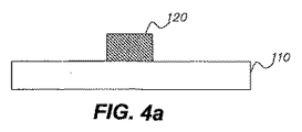
図4aと4bは、本発明に基づいて受理基板にアニールされ、転写されたナノ粒子層の一部分を有するドナーエレメントの断面図を示す。反射防止層65とリリース層75は、ドナー基板50の第一面側に堆積される。赤外(IR)吸収層80がリリース層75の頂部にコーティングされ、レーザ光を吸収して熱に変換する。金属ナノ粒子層90は、溶液で調製され、IR吸収層80上に均一に堆積される。次いで、ドナーエレメント100を配置するに当たり、金属ナノ粒子層90が受理基板110と緊密に接触するよう配置される。レーザビーム26を活性化して、レーザ光がドナーエレメント100を照射するようにする。レーザ光が吸収され、エネルギー吸収層80の選択された部分が加熱される。従ってナノ粒子層90が十分なレベルまで加熱され、ナノ粒子がアニールされ、金属導体フィルム120が形成される。次いでドナーエレメント100と受理基板110とを分離するに当たり、ナノ粒子層90の一部がレーザで照射され、加熱され、ドナーエレメント100から受理基板110にナノ粒子が分離され、転写されるように行われ、電気導体のパターンが受理基板に110上に形成される。一方、ナノ粒子層の一部は、レーザで照射されずに、ドナーエレメント100に付着したままで残置される。
4a and 4b show cross-sectional views of a donor element having a portion of a nanoparticle layer that has been annealed and transferred to a receiving substrate in accordance with the present invention. The
受理基板110は、有機固形物でも、無機固形物でも、あるいは有機固形物と無機固形物の組み合わせたものでも、ドナーエレメント100から金属導電性フィルムを受理する表面を提供するものであればなんでもよく、硬質性のものでも可撓性のものでもよい。典型的な基板材料としては、ガラス、プラスチック、金属、セラミック、半導体、金属酸化物、半導体酸化物、半導体窒化物、またはこれらの組み合わせ物が挙げられる。受理基板110は、これらの材料の均一混合物、これらの材料のコンポジット、またはこれらの材料を多層構造としたものでよい。受理基板110は、OLED基板、すなわち、OLED装置を製造するのに一般に使用される基板、例えば、アクティブマトリックス型低温ポリシリコンTFT基板でよい。受理基板110は、また、光透過型基板または不透明型基板のいずれでもよい。受理基板110には、転写段階の操作に先立って他の層で何らかのコーティングを施すこともできる。
The receiving
本発明とその利点は以下の実施例を参照すれば、一層理解が深まることと思われる。 The invention and its advantages will be better understood with reference to the following examples.
<実施例1>
ドナーエレメントを以下のように構成して作製した。
<Example 1>
The donor element was constructed as follows.
40mmのシリコンの反射防止層と40mmのクロムの吸収層とを、その順序で51μmのポリイミドドナー基板に真空堆積した。20%の2〜4nmサイズの金ナノ粒子と1〜2%のIR吸収色素とを40/60のエタノール/トルエン混合溶液に溶解し、1cc/平方フィートの湿潤塗布量で前記クロムにコーティングした。次ぎに、サンプルを室温で10分間乾燥し、約300〜500nmの最終厚さを得た。 A 40 mm silicon antireflective layer and a 40 mm chromium absorber layer were vacuum deposited in that order on a 51 μm polyimide donor substrate. 20% 2-4 nm size gold nanoparticles and 1-2% IR absorbing dye were dissolved in a 40/60 ethanol / toluene mixed solution and coated on the chromium with a wet coating weight of 1 cc / square foot. The sample was then dried at room temperature for 10 minutes to obtain a final thickness of about 300-500 nm.
(受理基板)
本発明に使用された受理基板は、表面の受理面に0.3μmのゼラチンをコーティングした4ミル厚さのPETフィルムであった。
(Receiving board)
The receiving substrate used in the present invention was a PET film having a thickness of 4 mils with a receiving surface coated with 0.3 μm gelatin.
(金属ナノ粒子層のアニールと転写)
金属ナノ粒子層を受理基板のゲル層と緊密に接触させて配置し、真空を使用して両層をしっかりと保持する。アニールと転写が望ましい領域では、被覆されたナノ粒子を波長830nmと最大出力600mWを有するレーザライタを使ってアニールし、既定の画像に従ってドナー支持板の第二面側からスキャンすることによってパターンを書き込む。スキャン速度の設定は、被覆された基板に約1.3J/cm2のエネルギーレベルでレーザが露光するように行われた。ドナーエレメントと受理基板を徐々に分離するに当たって、ナノ粒子層のその部分がレーザで照射され、加熱され、ドナー基板から受理基板に転写されるようにする。一方、ナノ粒子の層のある一部は、レーザで照射されないようにし、ドナー基板に付着したままで残置される。
(Annealing and transfer of metal nanoparticle layer)
The metal nanoparticle layer is placed in intimate contact with the gel layer of the receiving substrate and a vacuum is used to hold both layers firmly. In areas where annealing and transfer are desired, the coated nanoparticles are annealed using a laser writer having a wavelength of 830 nm and a maximum output of 600 mW, and the pattern is written by scanning from the second side of the donor support plate according to a predetermined image. . The scan speed was set so that the laser exposed to the coated substrate at an energy level of about 1.3 J / cm 2 . In gradually separating the donor element and the receiving substrate, that portion of the nanoparticle layer is irradiated with a laser, heated and transferred from the donor substrate to the receiving substrate. On the other hand, a part of the nanoparticle layer is left unattached to the donor substrate so that it is not irradiated with the laser.
<実施例2>
本発明の要件を満足するドナーエレメントと受理基板を、実施例1と同じように構成して作製した。但し、相違は、20%の50〜70nmサイズの銀ナノ粒子(ミネソタ州セントポールのCIMAナノテク(Nanotech)社から入手)を、2%のIR吸収色素を含むエチレングリコール/ブチルエーテルアセテート溶液に溶解したことである。
<Example 2>
A donor element and a receiving substrate that satisfy the requirements of the present invention were constructed in the same manner as in Example 1. However, the difference is that 20% 50-70 nm size silver nanoparticles (obtained from CIMA Nanotech, St. Paul, Minn.) Were dissolved in an ethylene glycol / butyl ether acetate solution containing 2% IR absorbing dye. That is.
<実施例3>
本発明の要件を満足するドナーエレメントと受理基板を、実施例1と同じように構成して作製した。但し、相違は、20%の50〜70nmサイズの銀ナノ粒子(ミネソタ州セントポールのCIMAナノテク(Nanotech)社から入手)を、2%のIR吸収色素を含む水/エタノール混合溶媒に溶解したことである。
ゲル被覆PET上にパターニングされたAu導体とAg導体をレーザでアニールし、転写して得られた結果は、以下の表1に示される。
<Example 3>
A donor element and a receiving substrate that satisfy the requirements of the present invention were constructed in the same manner as in Example 1. However, the difference was that 20% 50-70 nm size silver nanoparticles (obtained from CIMA Nanotech, St. Paul, Minn.) Were dissolved in a water / ethanol mixed solvent containing 2% IR absorbing dye. It is.
Table 1 below shows the results obtained by annealing and transferring the Au conductor and Ag conductor patterned on the gel-coated PET with a laser.
表1が示すのは、レーザ転写・アニールを行うと、ゲル被覆のPETに転写された金属層の抵抗率がまさに導体状態までに低下するということである。レーザに照射されなかったナノ粒子層は、焼結が欠けているのでドナー基板に非導体のままで残置する。 Table 1 shows that when laser transfer / annealing is performed, the resistivity of the metal layer transferred to the gel-coated PET is reduced to the state of a conductor. The nanoparticle layer that has not been irradiated with the laser is left unconductored on the donor substrate because of lack of sintering.
10 レーザ印刷装置、14 レーザ、18 基板、22 ガルバノメータ、24 fθレンズ、26 レーザビーム、28 コンピュータ、30 レーザ出力制御ライン、32 移動台、40 ポリゴン、45 ドナー基板、46 リニア移動装置、50 ドナー基板、60 マルチチャネル印刷ヘッド、65 反射防止層、70 回転ドラム、72 光ファイバ、75 リリース層、80 吸収層、90 ナノ粒子層、100 ドナーエレメント、110 受理基板、120 金属導体フィルム。 10 laser printing device, 14 laser, 18 substrate, 22 galvanometer, 24 fθ lens, 26 laser beam, 28 computer, 30 laser output control line, 32 moving table, 40 polygon, 45 donor substrate, 46 linear moving device, 50 donor substrate , 60 multi-channel print head, 65 anti-reflection layer, 70 rotating drum, 72 optical fiber, 75 release layer, 80 absorbing layer, 90 nanoparticle layer, 100 donor element, 110 receiving substrate, 120 metal conductor film.
Claims (43)
電導材料である金属ナノ粒子を形成するステップと、
ドナー基板を形成するステップと、
前記ドナー基板の第一面側に光吸収材料の層を堆積するステップと、
前記光吸収材料上に前記金属ナノ粒子を堆積するステップと、
前記金属ナノ粒子層を前記受理基板と緊密に接触して配置するステップと、
前記ドナー基板と前記受理基板の間に形成されたサンドイッチに、レーザで、パターンを書き込み、前記ナノ粒子層から得られる金属ナノ粒子を前記受理基板にアニールし、転写して前記受理基板の上に電気導体の前記パターンを形成するステップと、
を備えることを特徴とする方法。 A method of forming an electric conductor pattern on a receiving substrate is as follows:
Forming metal nanoparticles that are conductive materials;
Forming a donor substrate; and
Depositing a layer of light absorbing material on the first surface side of the donor substrate;
Depositing the metal nanoparticles on the light absorbing material;
Placing the metal nanoparticle layer in intimate contact with the receiving substrate;
The sandwich formed between the donor substrate and the receiving substrate is written with a laser with a pattern, the metal nanoparticles obtained from the nanoparticle layer are annealed to the receiving substrate, transferred, and transferred onto the receiving substrate. Forming the pattern of electrical conductors;
A method comprising the steps of:
電導材料である金属ナノ粒子を形成するステップと、
ドナー基板を形成するステップと、
前記ドナー基板の第一面側にリリース材料の層を堆積するステップと、
前記リリース材料上に光吸収材料を堆積するステップと、
前記光吸収材料上に前記金属ナノ粒子を堆積するステップと、
前記金属ナノ粒子層を前記受理基板と緊密に接触して配置するステップと、
前記ドナー基板と前記受理基板の間に形成されたサンドイッチに、レーザで、パターンを書き込み、前記ナノ粒子層から得られる金属ナノ粒子を前記受理基板にアニールし、転写して前記受理基板の上に電気導体の前記パターンを形成するステップと、
を備えることを特徴とする方法。 A method of forming an electric conductor pattern on a receiving substrate is as follows:
Forming metal nanoparticles that are conductive materials;
Forming a donor substrate; and
Depositing a layer of release material on the first side of the donor substrate;
Depositing a light absorbing material on the release material;
Depositing the metal nanoparticles on the light absorbing material;
Placing the metal nanoparticle layer in intimate contact with the receiving substrate;
The sandwich formed between the donor substrate and the receiving substrate is written with a laser with a pattern, the metal nanoparticles obtained from the nanoparticle layer are annealed to the receiving substrate, transferred, and transferred onto the receiving substrate. Forming the pattern of electrical conductors;
A method comprising the steps of:
金属ナノ粒子と光吸収性部分基とを一緒にする攪拌機と、
前記混合物をドナー基板にコーティングする塗工機と、
前記パターンを前記コーティングされたドナー基板から転写するレーザと、
を備えることを特徴とする装置。 An apparatus for forming an electric conductor pattern on a receiving substrate,
A stirrer that combines the metal nanoparticles and the light absorbing partial groups;
A coating machine for coating the mixture on the donor substrate;
A laser that transfers the pattern from the coated donor substrate;
A device comprising:
電導材料である金属ナノ粒子を形成するステップと、
ドナー基板を形成するステップと、
前記金属ナノ粒子を光吸収性部分基と混合するステップと、
前記金属ナノ粒子と前記光吸収性部分基とを前記ドナー基板の第一面の側に堆積するステップと、
前記金属ナノ粒子層と前記光吸収性部分基とを前記受理基板と緊密に接触して配置するステップと、
前記ドナー基板と前記受理基板の間に形成されたサンドイッチに、レーザで、パターンを書き込み、前記ナノ粒子層から得られる金属ナノ粒子を前記受理基板にアニールし、転写し、前記受理基板の上に電気導体の前記パターンを形成するステップと、
を備えることを特徴とする方法。 A method of forming an electric conductor pattern on a receiving substrate is as follows:
Forming metal nanoparticles that are conductive materials;
Forming a donor substrate; and
Mixing the metal nanoparticles with light absorbing partial groups;
Depositing the metal nanoparticles and the light absorbing partial groups on the first surface side of the donor substrate;
Placing the metal nanoparticle layer and the light absorbing partial group in intimate contact with the receiving substrate;
The sandwich formed between the donor substrate and the receiving substrate is written with a laser with a pattern, and the metal nanoparticles obtained from the nanoparticle layer are annealed to the receiving substrate, transferred, and transferred onto the receiving substrate. Forming the pattern of electrical conductors;
A method comprising the steps of:
Applications Claiming Priority (2)
| Application Number | Priority Date | Filing Date | Title |
|---|---|---|---|
| US11/130,772 US7648741B2 (en) | 2005-05-17 | 2005-05-17 | Forming a patterned metal layer using laser induced thermal transfer method |
| PCT/US2006/017288 WO2006124320A1 (en) | 2005-05-17 | 2006-05-02 | A patterned metal layer using thermal transfer |
Publications (2)
| Publication Number | Publication Date |
|---|---|
| JP2008541481A true JP2008541481A (en) | 2008-11-20 |
| JP2008541481A5 JP2008541481A5 (en) | 2009-02-12 |
Family
ID=36938060
Family Applications (1)
| Application Number | Title | Priority Date | Filing Date |
|---|---|---|---|
| JP2008512331A Withdrawn JP2008541481A (en) | 2005-05-17 | 2006-05-02 | Patterned metal layer formed using thermal transfer |
Country Status (6)
| Country | Link |
|---|---|
| US (1) | US7648741B2 (en) |
| EP (1) | EP1884146A1 (en) |
| JP (1) | JP2008541481A (en) |
| KR (1) | KR20080007465A (en) |
| CN (1) | CN100576970C (en) |
| WO (1) | WO2006124320A1 (en) |
Families Citing this family (19)
| Publication number | Priority date | Publication date | Assignee | Title |
|---|---|---|---|---|
| JP2007035742A (en) * | 2005-07-25 | 2007-02-08 | Seiko Epson Corp | Thin-film transistor forming method |
| US8084101B2 (en) * | 2006-08-01 | 2011-12-27 | The Board of Regents of the Nevada Systems of Higher Education on behalf of the University of Nevada, Las Vegas | Fabrication of patterned and ordered nanoparticles |
| CA2674702A1 (en) * | 2007-01-05 | 2008-07-10 | Basf Se | Method for producing electrically conductive surfaces |
| US7666567B2 (en) * | 2007-10-23 | 2010-02-23 | E. I. Du Pont De Nemours And Company | Negative imaging method for providing a patterned metal layer having high conductivity |
| TW201001624A (en) * | 2008-01-24 | 2010-01-01 | Soligie Inc | Silicon thin film transistors, systems, and methods of making same |
| CN101519184B (en) * | 2008-02-29 | 2012-05-23 | 财团法人工业技术研究院 | Method for manufacturing application substrate through photo-thermal effect |
| KR101529111B1 (en) * | 2008-06-16 | 2015-06-16 | 도레이 카부시키가이샤 | Patterning method, device manufacturing method using the patterning method, and device |
| FR2946639B1 (en) * | 2009-06-12 | 2011-07-15 | Saint Gobain | THIN LAYER DEPOSITION METHOD AND PRODUCT OBTAINED |
| US20110027499A1 (en) * | 2009-07-30 | 2011-02-03 | International Business Machines Corporation | Radiation-assisted nanoparticle printing |
| DE102009050199A1 (en) * | 2009-10-21 | 2011-04-28 | Giesecke & Devrient Gmbh | Production of conductor structures on plastic films using nanoinks |
| DE102010015659A1 (en) * | 2010-04-20 | 2011-10-20 | Giesecke & Devrient Gmbh | Transfer method for the production of conductor structures by means of nanoinks |
| FR2980279B1 (en) * | 2011-09-20 | 2013-10-11 | Soitec Silicon On Insulator | METHOD FOR MANUFACTURING A COMPOSITE STRUCTURE TO BE SEPARATED BY EXFOLIATION |
| KR20140140188A (en) * | 2013-05-28 | 2014-12-09 | 삼성디스플레이 주식회사 | Donor substrate, method for fabricating the same and method for forming transfer pattern using the same |
| SG11201609740UA (en) * | 2014-05-27 | 2016-12-29 | Yissum Res Dev Co | Method of fabricating metallic patterns and objects |
| WO2016166590A1 (en) * | 2015-04-13 | 2016-10-20 | Jan Franck | Device and method for producing printed circuit boards for electrical and/or electronic circuits |
| FR3035540B1 (en) | 2015-04-27 | 2017-04-28 | Centre Nat Rech Scient | PRINTING METHOD USING TWO LASERS |
| US9776442B2 (en) | 2015-12-30 | 2017-10-03 | Palo Alto Research Center Incorporated | Single pass imaging using rapidly addressable laser lamination |
| EP3663090A1 (en) * | 2018-12-04 | 2020-06-10 | Nederlandse Organisatie voor toegepast- natuurwetenschappelijk onderzoek TNO | High resolution laser induced forward transfer |
| CN117465081A (en) * | 2023-10-12 | 2024-01-30 | 广东工业大学 | High-absorbance composite membrane and application thereof in laser-induced transfer |
Family Cites Families (42)
| Publication number | Priority date | Publication date | Assignee | Title |
|---|---|---|---|---|
| US4541830A (en) | 1982-11-11 | 1985-09-17 | Matsushita Electric Industrial Co., Ltd. | Dye transfer sheets for heat-sensitive recording |
| US4698651A (en) | 1985-12-24 | 1987-10-06 | Eastman Kodak Company | Magenta dye-donor element used in thermal dye transfer |
| US4695287A (en) | 1985-12-24 | 1987-09-22 | Eastman Kodak Company | Cyan dye-donor element used in thermal dye transfer |
| US4701439A (en) | 1985-12-24 | 1987-10-20 | Eastman Kodak Company | Yellow dye-donor element used in thermal dye transfer |
| US4743582A (en) | 1986-10-06 | 1988-05-10 | Eastman Kodak Company | N-alkyl-or n-aryl-aminopyrazolone merocyanine dye-donor element used in thermal dye transfer |
| US4757046A (en) | 1986-10-06 | 1988-07-12 | Eastman Kodak Company | Merocyanine dye-donor element used in thermal dye transfer |
| US4769360A (en) | 1987-09-14 | 1988-09-06 | Eastman Kodak Company | Cyan dye-donor element for thermal dye transfer |
| US4753922A (en) | 1987-11-20 | 1988-06-28 | Eastman Kodak Company | Neutral-black dye-donor element for thermal dye transfer |
| US4973572A (en) | 1987-12-21 | 1990-11-27 | Eastman Kodak Company | Infrared absorbing cyanine dyes for dye-donor element used in laser-induced thermal dye transfer |
| US4900130A (en) | 1988-10-07 | 1990-02-13 | Eastman Kodak Company | Method of scanning |
| US5171650A (en) | 1990-10-04 | 1992-12-15 | Graphics Technology International, Inc. | Ablation-transfer imaging/recording |
| US5256506A (en) | 1990-10-04 | 1993-10-26 | Graphics Technology International Inc. | Ablation-transfer imaging/recording |
| US4950639A (en) | 1989-06-16 | 1990-08-21 | Eastman Kodak Company | Infrared absorbing bis(aminoaryl)polymethine dyes for dye-donor element used in laser-induced thermal dye transfer |
| US4948777A (en) | 1989-06-16 | 1990-08-14 | Eastman Kodak Company | Infrared absorbing bis(chalcogenopyrylo)polymethine dyes for dye-donor element used in laser-induced thermal dye transfer |
| US4942141A (en) | 1989-06-16 | 1990-07-17 | Eastman Kodak Company | Infrared absorbing squarylium dyes for dye-donor element used in laser-induced thermal dye transfer |
| US4948776A (en) | 1989-06-16 | 1990-08-14 | Eastman Kodak Company | Infrared absorbing chalcogenopyrylo-arylidene dyes for dye-donor element used in laser-induced thermal dye transfer |
| US4950640A (en) | 1989-06-16 | 1990-08-21 | Eastman Kodak Company | Infrared absorbing merocyanine dyes for dye-donor element used in laser-induced thermal dye transfer |
| US4948778A (en) | 1989-06-20 | 1990-08-14 | Eastman Kodak Company | Infrared absorbing oxyindolizine dyes for dye-donor element used in laser-induced thermal dye transfer |
| US4912083A (en) | 1989-06-20 | 1990-03-27 | Eastman Kodak Company | Infrared absorbing ferrous complexes for dye-donor element used in laser-induced thermal dye transfer |
| US5036040A (en) | 1989-06-20 | 1991-07-30 | Eastman Kodak Company | Infrared absorbing nickel-dithiolene dye complexes for dye-donor element used in laser-induced thermal dye transfer |
| US4952552A (en) | 1989-06-20 | 1990-08-28 | Eastman Kodak Company | Infrared absorbing quinoid dyes for dye-donor element used in laser-induced thermal dye transfer |
| US5244770A (en) | 1991-10-23 | 1993-09-14 | Eastman Kodak Company | Donor element for laser color transfer |
| US5292559A (en) | 1992-01-10 | 1994-03-08 | Amp Incorporated | Laser transfer process |
| US5691098A (en) | 1996-04-03 | 1997-11-25 | Minnesota Mining And Manufacturing Company | Laser-Induced mass transfer imaging materials utilizing diazo compounds |
| US5725989A (en) | 1996-04-15 | 1998-03-10 | Chang; Jeffrey C. | Laser addressable thermal transfer imaging element with an interlayer |
| US5800960A (en) | 1996-10-24 | 1998-09-01 | Eastman Kodak Company | Uniform background for color transfer |
| US6143451A (en) * | 1996-11-26 | 2000-11-07 | E. I. Du Pont De Nemours And Company | Imaged laserable assemblages and associated processes with high speed and durable image-transfer characteristics for laser-induced thermal transfer |
| US6031561A (en) * | 1997-04-22 | 2000-02-29 | Eastman Kodak Company | Printer system having a plurality of light sources of different wavelengths |
| US6097416A (en) | 1997-11-10 | 2000-08-01 | Eastman Kodak Company | Method for reducing donor utilization for radiation-induced colorant transfer |
| US6252621B1 (en) | 1998-08-03 | 2001-06-26 | Eastman Kodak Company | Printing lenticular images |
| US6169565B1 (en) * | 1999-03-31 | 2001-01-02 | Eastman Kodak Company | Laser printer utilizing a spatial light modulator |
| US6165671A (en) * | 1999-12-30 | 2000-12-26 | Eastman Kodak Company | Laser donor element |
| JP5008216B2 (en) * | 2000-10-13 | 2012-08-22 | 株式会社アルバック | Inkjet ink manufacturing method |
| AU2002239581B2 (en) * | 2000-12-15 | 2006-09-28 | The Arizona Board Of Regents On Behalf Of The University Of Arizona | Method for patterning metal using nanoparticle containing precursors |
| JP4066621B2 (en) | 2001-07-19 | 2008-03-26 | 富士通株式会社 | Full-text search system and full-text search program |
| US6703111B2 (en) | 2001-10-25 | 2004-03-09 | Eastman Kodak Company | Laser thermal imaging process, dye, and element |
| US6770549B2 (en) | 2002-05-08 | 2004-08-03 | Lucent Technologies Inc. | Forming patterned thin film metal layers |
| US6939660B2 (en) * | 2002-08-02 | 2005-09-06 | Eastman Kodak Company | Laser thermal transfer donor including a separate dopant layer |
| US6890627B2 (en) | 2002-08-02 | 2005-05-10 | Eastman Kodak Company | Laser thermal transfer from a donor element containing a hole-transporting layer |
| TWI265762B (en) * | 2003-01-14 | 2006-11-01 | Sharp Kk | Wiring material, wiring substrate and manufacturing method thereof, display panel, fine particle thin film material, substrate including thin film layer and manufacturing method thereof |
| US6790594B1 (en) * | 2003-03-20 | 2004-09-14 | Eastman Kodak Company | High absorption donor substrate coatable with organic layer(s) transferrable in response to incident laser light |
| US20060003262A1 (en) | 2004-06-30 | 2006-01-05 | Eastman Kodak Company | Forming electrical conductors on a substrate |
-
2005
- 2005-05-17 US US11/130,772 patent/US7648741B2/en not_active Expired - Fee Related
-
2006
- 2006-05-02 CN CN200680016938A patent/CN100576970C/en not_active Expired - Fee Related
- 2006-05-02 WO PCT/US2006/017288 patent/WO2006124320A1/en active Application Filing
- 2006-05-02 KR KR1020077026589A patent/KR20080007465A/en not_active Application Discontinuation
- 2006-05-02 JP JP2008512331A patent/JP2008541481A/en not_active Withdrawn
- 2006-05-02 EP EP06759105A patent/EP1884146A1/en not_active Withdrawn
Also Published As
| Publication number | Publication date |
|---|---|
| CN101199245A (en) | 2008-06-11 |
| US20060263725A1 (en) | 2006-11-23 |
| KR20080007465A (en) | 2008-01-21 |
| CN100576970C (en) | 2009-12-30 |
| US7648741B2 (en) | 2010-01-19 |
| WO2006124320A1 (en) | 2006-11-23 |
| EP1884146A1 (en) | 2008-02-06 |
Similar Documents
| Publication | Publication Date | Title |
|---|---|---|
| JP2008541481A (en) | Patterned metal layer formed using thermal transfer | |
| JP2008505494A (en) | Formation of electrical conductors on substrates | |
| CN102448623B (en) | Metal ink | |
| Kang et al. | One-step fabrication of copper electrode by laser-induced direct local reduction and agglomeration of copper oxide nanoparticle | |
| CA2588343C (en) | Electrical, plating and catalytic uses of metal nanomaterial compositions | |
| US20170027063A1 (en) | Electrical, plating and catalytic uses of metal nanomaterial compositions | |
| Lee et al. | Effect of solvent and PVP on electrode conductivity in laser-induced reduction process | |
| US20030146019A1 (en) | Board and ink used for forming conductive pattern, and method using thereof | |
| US20070279182A1 (en) | Printed resistors and processes for forming same | |
| US10957615B2 (en) | Laser-seeding for electro-conductive plating | |
| EP2150417A1 (en) | Metallic ink | |
| CN109270798A (en) | The method and copper ion ink of the anti-oxidant copper micro-structure of femtosecond laser direct write | |
| KR101808741B1 (en) | Method for forming conductive layer patterns by inkjet-printing | |
| JP2014075461A (en) | Conductive wiring and method for fabricating conductive wiring | |
| Pasquet et al. | Selective Laser Decomposition of Silver Oxalate: A New Way of Preparing and Shaping Metallic Silver Patterns | |
| US20140356997A1 (en) | Donor substrate, method of manufacturing the same, and method of forming transfer pattern using the same | |
| KR20210007059A (en) | Method of manufacturing flexible electrode and flexible electrode manufactured by the same | |
| Jose et al. | Study on the Conventional Versus Photonic (IPL) Sintering of Copper Nanoparticle (Cu NPs) Inks on Different Flexible Substrates | |
| Vorobyev et al. | Nanomaterials: Laser‐Induced Nano/Microfabrications | |
| Ha et al. | Femtosecond laser multiple pulse-induced thermochemical copper precipitation from glyoxylic acid copper complex ink with surfactant | |
| Watanabe et al. | Laser direct writing of conductive micropatterns using copper nanoparticle ink toward 3D interconnection |
Legal Events
| Date | Code | Title | Description |
|---|---|---|---|
| A521 | Written amendment |
Free format text: JAPANESE INTERMEDIATE CODE: A523 Effective date: 20081208 |
|
| A621 | Written request for application examination |
Free format text: JAPANESE INTERMEDIATE CODE: A621 Effective date: 20081208 |
|
| A761 | Written withdrawal of application |
Free format text: JAPANESE INTERMEDIATE CODE: A761 Effective date: 20100304 |