JP2008536294A - High performance light emitting diodes (LEDs), monochromatic or multicolored, grown on patterned substrates - Google Patents
High performance light emitting diodes (LEDs), monochromatic or multicolored, grown on patterned substrates Download PDFInfo
- Publication number
- JP2008536294A JP2008536294A JP2007558124A JP2007558124A JP2008536294A JP 2008536294 A JP2008536294 A JP 2008536294A JP 2007558124 A JP2007558124 A JP 2007558124A JP 2007558124 A JP2007558124 A JP 2007558124A JP 2008536294 A JP2008536294 A JP 2008536294A
- Authority
- JP
- Japan
- Prior art keywords
- led
- layer
- mask
- patterned
- active
- Prior art date
- Legal status (The legal status is an assumption and is not a legal conclusion. Google has not performed a legal analysis and makes no representation as to the accuracy of the status listed.)
- Pending
Links
Images


Classifications
-
- H—ELECTRICITY
- H01—ELECTRIC ELEMENTS
- H01L—SEMICONDUCTOR DEVICES NOT COVERED BY CLASS H10
- H01L33/00—Semiconductor devices with at least one potential-jump barrier or surface barrier specially adapted for light emission; Processes or apparatus specially adapted for the manufacture or treatment thereof or of parts thereof; Details thereof
- H01L33/02—Semiconductor devices with at least one potential-jump barrier or surface barrier specially adapted for light emission; Processes or apparatus specially adapted for the manufacture or treatment thereof or of parts thereof; Details thereof characterised by the semiconductor bodies
- H01L33/20—Semiconductor devices with at least one potential-jump barrier or surface barrier specially adapted for light emission; Processes or apparatus specially adapted for the manufacture or treatment thereof or of parts thereof; Details thereof characterised by the semiconductor bodies with a particular shape, e.g. curved or truncated substrate
-
- H—ELECTRICITY
- H01—ELECTRIC ELEMENTS
- H01L—SEMICONDUCTOR DEVICES NOT COVERED BY CLASS H10
- H01L2933/00—Details relating to devices covered by the group H01L33/00 but not provided for in its subgroups
- H01L2933/0083—Periodic patterns for optical field-shaping in or on the semiconductor body or semiconductor body package, e.g. photonic bandgap structures
-
- H—ELECTRICITY
- H01—ELECTRIC ELEMENTS
- H01L—SEMICONDUCTOR DEVICES NOT COVERED BY CLASS H10
- H01L33/00—Semiconductor devices with at least one potential-jump barrier or surface barrier specially adapted for light emission; Processes or apparatus specially adapted for the manufacture or treatment thereof or of parts thereof; Details thereof
- H01L33/02—Semiconductor devices with at least one potential-jump barrier or surface barrier specially adapted for light emission; Processes or apparatus specially adapted for the manufacture or treatment thereof or of parts thereof; Details thereof characterised by the semiconductor bodies
- H01L33/20—Semiconductor devices with at least one potential-jump barrier or surface barrier specially adapted for light emission; Processes or apparatus specially adapted for the manufacture or treatment thereof or of parts thereof; Details thereof characterised by the semiconductor bodies with a particular shape, e.g. curved or truncated substrate
- H01L33/22—Roughened surfaces, e.g. at the interface between epitaxial layers
-
- H—ELECTRICITY
- H01—ELECTRIC ELEMENTS
- H01L—SEMICONDUCTOR DEVICES NOT COVERED BY CLASS H10
- H01L33/00—Semiconductor devices with at least one potential-jump barrier or surface barrier specially adapted for light emission; Processes or apparatus specially adapted for the manufacture or treatment thereof or of parts thereof; Details thereof
- H01L33/02—Semiconductor devices with at least one potential-jump barrier or surface barrier specially adapted for light emission; Processes or apparatus specially adapted for the manufacture or treatment thereof or of parts thereof; Details thereof characterised by the semiconductor bodies
- H01L33/20—Semiconductor devices with at least one potential-jump barrier or surface barrier specially adapted for light emission; Processes or apparatus specially adapted for the manufacture or treatment thereof or of parts thereof; Details thereof characterised by the semiconductor bodies with a particular shape, e.g. curved or truncated substrate
- H01L33/24—Semiconductor devices with at least one potential-jump barrier or surface barrier specially adapted for light emission; Processes or apparatus specially adapted for the manufacture or treatment thereof or of parts thereof; Details thereof characterised by the semiconductor bodies with a particular shape, e.g. curved or truncated substrate of the light emitting region, e.g. non-planar junction
Abstract
高い抽出効率を有する単色またはマルチカラーの発光ダイオード(LED)は、基板と、基板上に形成されたバッファ層と、バッファ層の上部に堆積された1つ以上のパターニングされた層と、パターニングされた層の上または層の間に形成された1つ以上のアクティブ層から構成される。上記発光ダイオードは、例えば、横方向エピタキシャル成長(LEO)によるものであり、1つ以上の発光種(例えば、量子井戸)を含む。パターニングされた層は、パターニングされ穿孔または貫通されたマスク(絶縁材料または半導性材料または金属材料から構成されている)と、マスク内のホールを充填する材料とを備えている。パターニングされた層は、アクティブ層との屈折率のコントラストに起因して光閉じ込め層として機能し、かつ/またはマスクと上記マスク内のホールを充填する材料との間の屈折率の変化に起因して埋め込み回折格子として機能する。A single color or multi-color light emitting diode (LED) having high extraction efficiency is patterned with a substrate, a buffer layer formed on the substrate, and one or more patterned layers deposited on top of the buffer layer. One or more active layers formed on or between layers. The light emitting diode is, for example, by lateral epitaxial growth (LEO) and includes one or more light emitting species (eg, quantum wells). The patterned layer comprises a patterned and perforated or penetrated mask (consisting of an insulating or semiconductive material or metal material) and a material that fills the holes in the mask. The patterned layer functions as a light confinement layer due to the refractive index contrast with the active layer and / or due to the refractive index change between the mask and the material filling the holes in the mask. And function as a buried diffraction grating.
Description
(関連出願の引用)
本出願は、同一出願人による以下の同時継続出願の優先権を主張する:
米国特許出願第11/067,910号、2005年2月28日出願、Claude C.A.Weisbuch、Aurelien J.F.David、James S.Speck、およびSteven P.DenBaars、題名「SINGLE OR MULTI−COLOR HIGH EFFICIENCY LIGHT EMITTING DIODE(LED) BY GROWTH OVER A PATTERNED SUBSTRATE」、代理人管理番号第30794.122−US−01(2004−145−1)号
上記出願は、参考のために本明細書に援用される。
(Citation of related application)
This application claims the priority of the following co-pending applications by the same applicant:
US patent application Ser. No. 11 / 067,910, filed Feb. 28, 2005, Claud C. A. Weisbuch, Aurelian J. et al. F. David, James S. Speck and Steven P. DenBaars, title “SINGLE OR MULTI-COLOR HIGH EFFICICY LIGHT MITTING DIODE (LED) BY GROWTH OVER A PATTERNED SUBSTRATE”, agent management number 30014. Is incorporated herein by reference.
本出願はまた、同一出願人による以下の同時継続出願にも関連する:
米国特許出願第10/938,704号、2004年9月10日出願、Carole Schwach、Claude C.A.Weisbuch、Steven P.DenBaars、Henri Benisty、およびShuji Nakamura、題名「WHITE、SINGLE OR MULTI−COLOR LIGHT EMITTING DIODES BY RECYCLING GUIDED MODES」、代理人管理番号第30794.115−US−01(2004−064−1)号、
米国特許出願第11/067,957号、2005年2月28日出願、Claude C.A.Weisbuch、Aurelien J.F.David、James S.Speck、およびSteven P.DenBaars、題名「HORIZONTAL EMITTING、VERTICAL EMITTING、BEAM SHAPED、DISTRIBUTED FEEDBACK(DFB) LASERS BY GROWTH OVER A PATTERNED SUBSTRATE」、代理人管理番号第30794.121−US−01(2005−144−1)号;ならびに
米国特許出願第11/067,956号、2005年2月28日出願、Claude C.A.Weisbuch、Aurelien J.F.David、およびSteven P.DenBaars、題名「HIGH EFFICIECY LIGHT EMITTING DIODE(LED) WITH OPTIMIZED PHOTONIC CRYSTAL EXTRACTOR」、代理人管理番号第30794.126−US−01(2005−198−1)号
上記出願は、参考のために本明細書に援用される。
This application is also related to the following co-pending applications by the same applicant:
US patent application Ser. No. 10 / 938,704, filed Sep. 10, 2004, Carole Schwach, Claud C. A. Weisbuch, Steven P. et al. DenBaars, Henri Benisty, and Shuji Nakamura, titles “WHITE, SINGLE OR MULTI-COLOR LIGHTING MITTING DIODES BY RECYCLING GUIDED MODES”, No. 4-US Pat.
US patent application Ser. No. 11 / 067,957, filed Feb. 28, 2005, Claud C. A. Weisbuch, Aurelian J. et al. F. David, James S. Speck and Steven P. DenBaars, titles “HORIZONTAL EMITTING, VERTICAL EMITTING, BEAM SHAPED, DISTRIBUTED FEEDBACK (DFB) LASTERS BY GROWTH OVER A patterned SUB121. Patent Application No. 11 / 067,956, filed February 28, 2005, Claud C. A. Weisbuch, Aurelian J. et al. F. David, and Steven P. DenBaars, titled "HIGH EFFICIECY LIGHT MITTING DIODE (LED) WITH OPTIMIZED PHOTOTONIC CRYSTAL EXTRACTOR", agent management number 30794.126-US-01 (2005-198-1) Incorporated.
(委託研究開発に関する陳述)
本発明は、University of California、Santa Barbara Solid State Lighting and Display Centerのメンバーカンパニーからの支援のもとでなされたものであり、上記メンバーカンパニーは、Stanley Electric Co.、Ltd.、Mitsubishi Chemical Corp.、Rohm Co.、Ltd.、Cree、Inc.、Matsushita Electric Works、Matsushita Electric Industrial Co.、およびSeoul Semiconductor Co.、Ltdを含む。
(Statement regarding contract research and development)
The present invention was made with the support of the member companies of University of California, Santa Barbara Solid State Lighting and Display Center, and the above member companies are based on Stanley Electric Co., Ltd. , Ltd.,. , Mitsubishi Chemical Corp. Rohm Co., Ltd. , Ltd.,. , Cree, Inc. , Matsushita Electric Works, Matsushita Electric Industrial Co., Ltd. , And Seol Semiconductor Co. , Ltd.
(本発明の背景)
(1.本発明の分野)
本発明は、発光ダイオード(LED)に関し、より詳細には、パターニングされた基板上の成長による単色またはマルチカラーのLEDに関する。
(Background of the present invention)
(1. Field of the Invention)
The present invention relates to light emitting diodes (LEDs), and more particularly to monochromatic or multicolored LEDs by growth on a patterned substrate.
(2.関連技術の記載)
発光ダイオード(LED)は、順方向に電気的にバイアスされたときに、誘導放出するように光を放出する半導体デバイスである。この効果は、エレクトロルミネセンスの一形態である。
(2. Description of related technology)
A light emitting diode (LED) is a semiconductor device that emits light so as to emit stimulated when electrically biased in the forward direction. This effect is a form of electroluminescence.
LEDは、不純物で含浸またはドープされた半導性材料のチップから構成され、pn接合と称される構造を形成する。順方向にバイアスされると、n領域から接合に電子が射出され、p領域からはホールが射出される。電子およびホールは、それらが再結合する際に、光子の形態で、エネルギーを解放する。光の波長、そしてその色は、pn接合を形成する材料のバンドギャップエネルギーに依存する。 An LED is composed of a chip of semiconductive material impregnated or doped with impurities, forming a structure called a pn junction. When biased in the forward direction, electrons are emitted from the n region to the junction, and holes are emitted from the p region. Electrons and holes release energy in the form of photons as they recombine. The wavelength of light and its color depend on the band gap energy of the material forming the pn junction.
半導体材料が改良されるにつれて、半導体デバイスの効率もまた改良されてきており、新しい波長範囲もまた、用いられるようになった。窒化ガリウム(GaN)ベースの発光体は、おそらく、様々な用途に対して最も有望である。GaNは、例えば、可変濃度のインジウム(In)と混合されたときに、紫外線(UV)から黄色スペクトルまでの効率的な照射を提供する。 As semiconductor materials have improved, the efficiency of semiconductor devices has also improved, and new wavelength ranges have also been used. Gallium nitride (GaN) based emitters are probably the most promising for various applications. GaN, for example, provides efficient illumination from the ultraviolet (UV) to the yellow spectrum when mixed with variable concentrations of indium (In).
不都合にも、半導体LED材料内で発光された光は、半導体−空気の界面における全内反射が原因で、ほとんどが損失する。典型的な半導体材料は、高い屈折率を有しているので、Snellの法則にしたがうと、光のほとんどは、材料内に捕獲され得、その結果、効率が低減される。LEDに対して適切な幾何学的配置を選択することにより、高い抽出効率が達成され得る。 Unfortunately, most of the light emitted in the semiconductor LED material is lost due to total internal reflection at the semiconductor-air interface. Since a typical semiconductor material has a high refractive index, according to Snell's law, most of the light can be trapped in the material, resulting in reduced efficiency. By choosing an appropriate geometry for the LED, high extraction efficiency can be achieved.
図1は、同質な発光材料10の断面図を示しており、これは、材料14内部で発光された光の一部12が、エスケープコーン16内に存在し、材料10から逃げ得る一方で、発光された光の大部分18が、材料10内に捕獲され、反射されることを示している。この状況において、反射された光18は、導波光モード(guided light mode)または導波モード(guided mode)と称される。なぜならば、この光18は、デバイス10内に閉じ込められ、材料10内において横方向にガイドされるからである。
FIG. 1 shows a cross-sectional view of a homogeneous
全内反射の影響を低減させるための1つの方法は、デバイスの表面のランダムなテクスチャを介して光の散乱または再分配を形成することであり、これは、デバイスの半導体−空気の界面における、複数の可変角度の入射を引き起こす。このアプローチは、高い内部効率と低い内部損失の結果として、発光効率を9〜30%向上させることが示されており、これは、光がデバイスから逃げる前に多数の光の経路を与える。 One way to reduce the effect of total internal reflection is to form light scattering or redistribution through a random texture on the surface of the device, which is at the semiconductor-air interface of the device, Causes multiple variable angles of incidence. This approach has been shown to increase luminous efficiency by 9-30% as a result of high internal efficiency and low internal loss, which provides multiple light paths before the light escapes from the device.
図2は、このコンセプトを示す半導体LED20の断面図であり、LED20の上面22は、テクスチャ加工されており、LED20の底面24は、反射体を備えており、空気は、屈折率n=1を有しており、LED20の半導体材料は、屈折率n=3.5を有している。LED20のテクスチャ加工された上面22は、幾何光学的アプローチで光の軌道をランダム化するために用いられる。
FIG. 2 is a cross-sectional view of a
捕獲される光の割合を低減させるための別の方法は、共振キャビティLED(RCLED)またはマイクロキャビティLED(MCLED)を用いることである。MCLEDは、「伝統的な」LEDを用いる既存のシステムよりも高い効率を有する固体発光システムを形成する機会を提供する。共振キャビティ内に利得媒体を組み込む結果として、MCLEDは、非常にコンパクトで指向性の光線を発光する。これらのデバイスの比較的高い抽出効率と比較的強い明るさは、従来のLEDに対するこれらの技術の主要な利点である。 Another way to reduce the percentage of light that is captured is to use a resonant cavity LED (RCLED) or a microcavity LED (MCLED). MCLEDs offer the opportunity to form solid state lighting systems that have higher efficiencies than existing systems that use “traditional” LEDs. As a result of incorporating the gain medium in the resonant cavity, MCLEDs emit very compact and directional light. The relatively high extraction efficiency and relatively strong brightness of these devices are the main advantages of these technologies over conventional LEDs.
抽出効率とは、特定のシステムによって生成された光子が「有用」な照射としてシステムから実際に出る能力を意味する。しかしながら、マイクロキャビティ構造はまた、導波モードおよび漏れモードへの非常に有効な放出にもつながるので、この比較的高い抽出効率は、40%の範囲に制限される。したがって、これらの導波モードが抽出され得るならば、有用であり得る。 Extraction efficiency refers to the ability of the photons generated by a particular system to actually exit the system as “useful” illumination. However, this relatively high extraction efficiency is limited to the 40% range, since the microcavity structure also leads to a very effective emission into guided and leaky modes. Therefore, it may be useful if these guided modes can be extracted.
上述のように、導波モードは、構造層の間の屈折率の違いに起因してデバイス平面内に導かれるモードである。漏れモードは、層を介して、空気または基板へと放射される。漏れモードは、それらのエネルギーが様々な損失機構(例えば、金属ミラー損失、自由キャリア吸収、アクティブ層による再吸収等)によって消散されるまでに、通常、界面において複数の全内反射を経て、デバイス内であちらこちらに動く際に、損失する。 As described above, the guided mode is a mode that is guided in the device plane due to a difference in refractive index between the structural layers. The leak mode is radiated through the layer to the air or substrate. Leaky modes typically involve multiple total internal reflections at the interface before their energy is dissipated by various loss mechanisms (eg, metal mirror loss, free carrier absorption, active layer reabsorption, etc.) You lose when you move from one place to another within.
図3は、放射モード、導波モード、漏れモードを示す半導体LED26の断面図であり、LED26は、基板28、バッファ層30、およびアクティブ層32を含んでおり、上記アクティブ層は、量子井戸(QW)34を含んでいる。放出された光の一部は、空気に向けて抽出36され、放射モード36を形成し、放出された光の一部は、デバイス26の様々な層を介することにより、基板28に漏れ38、漏れモード38を形成し、放出された光の一部は、アクティブ層32(またはアクティブ層32およびバッファ層30の両方)において反射され40、導波モード40を形成する。
FIG. 3 is a cross-sectional view of a
高性能なLEDを得るためには、構造の外への光の放射36を最適化し、漏れモード38および導波モード40の放出を最小化し、そして出来る限り、導波モードの放出40を再放出し、さらには漏れモード38の放出の一部を再放出することが必要である。本発明は、容易に製造可能な構造により、この目的を満たすことを目標としている。
In order to obtain a high performance LED, the
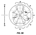
図4A〜図4Bおよび図5A〜図5Bは、マイクロキャビティ放出の構造(図4Aおよび図5A)およびシミュレーション(図4Bおよび図5B)を、窒化ガリウム(GaN)材料システムにおける、底部の金属または分布型ブラッグ反射体(DBR)ミラーと、上部における空気との単一の界面とによって、示している。図4Bおよび図5Bは、半導体内部の対数目盛りの角放出図(angular emission diagram)であり、図4Bは、図4Aの構造の放出を示しており、図5Bは、図5Aの構造の放出を示している。図4Bおよび図5Bの両方に対し、図の左半分は、TM(transverse magnetic)放出を示しており、右半分は、TE(transverse electric)偏向放出を示している。平面内のモノクロのダイポールのみが仮定されている。 4A-4B and 5A-5B illustrate the structure (FIGS. 4A and 5A) and simulation (FIGS. 4B and 5B) of the microcavity emission, bottom metal or distribution in a gallium nitride (GaN) material system. This is shown by a type Bragg reflector (DBR) mirror and a single interface with air at the top. 4B and 5B are an angular emission diagram of a logarithmic scale inside a semiconductor, FIG. 4B shows the emission of the structure of FIG. 4A, and FIG. 5B shows the emission of the structure of FIG. 5A. Show. For both FIG. 4B and FIG. 5B, the left half of the figure shows TM (transverse magnetic) emission and the right half shows TE (transverse electric) polarized emission. Only a monochrome dipole in the plane is assumed.
図4Aにおいて、構造は、金属ミラー42およびアクティブ層44を含んでおり、上記アクティブ層は、量子井戸46を含んでおり、上記構造は、3λ/4のキャビティであり、量子井戸46は、金属ミラー42のλ/4(48)に配置されている。図4Bにおいて、矢印50は、空気に向けての放出を示しており、その一方で、矢印52は、基板に向けての放出を示している。また、図4Bにおいて、ブレース36は、抽出された光を示しており、ブレース40は、導波モードを示している。
In FIG. 4A, the structure includes a
図5Aにおいて、構造は、バッファ54、7周期DBRミラー56、およびアクティブ層58を含んでおり、上記アクティブ層は、量子井戸60を含んでいる。ここで、構造は、λのキャビティであり、量子井戸60は、7周期DBRミラー56のλ/2(62)に配置されている。図5Bにおいて、矢印64は、空気に向けての放出を示しており、その一方で、矢印66は、基板に向けての放出を示している。また、図5Bにおいて、ブレース36は、抽出された光を示しており、ブレース38は、漏れモードを示しており、ブレース40は、導波モードを示している。
In FIG. 5A, the structure includes a
これらの構造からの抽出効率は、それぞれ、図4Aにおいて、空中で31%および24%であり、図5Aにおいて、エポキシ内で44%および27%である。 Extraction efficiencies from these structures are 31% and 24% in air in FIG. 4A and 44% and 27% in epoxy in FIG. 5A, respectively.
LEDのマイクロキャビティ抽出に関し、大幅な改善を得ようと試みるときに、ほとんどの材料システムでは、困難に直面する。図4Bおよび図5Bは、放出図を示しており、最適化されたGaNマイクロキャビティLEDの期待される効率がこれらから抽出されるが、以下の問題点を示している:
(i)エピタキシャルに成長された材料に対する屈折率コントラストは、特に、非常に重要な窒化物材料に対し、かなり制限されている。これは、図5AのDBRミラー56の構造において多数の漏れモードへの放出が見られるからであり、これは、図5AのDBRミラー56の構造の効率を、図4Aの金属ミラー42の効率よりも低くする。
(ii)表示された効率は、非常に薄い構造が考えられ、下位キャビティ(以下では、参照番号10で記載されている)をもたらすからこそ可能である。そのような薄いアクティブ層を得ることは、困難である。例えば、通常は、アクティブ層のための良い品質の材料を成長させる前に、窒化物の薄い(数ミクロンの)バッファ層を基板上に成長させる必要がある。窒化物材料(バッファ層およびアクティブ層)を基板からリフトオフすることは、既にデリケートな操作であるが、それに加え、図4Aに示されている薄い金属ミラー構造の優れた性能をもたらし得る良好な金属ミラーによって囲まれた薄い層を得ることが(すなわちバッファ層の一部または全部をさらに除去することが)、極めて困難だからである。
With respect to LED microcavity extraction, most material systems face difficulties when trying to obtain significant improvements. 4B and 5B show the emission diagrams, from which the expected efficiency of the optimized GaN microcavity LED is extracted, showing the following issues:
(I) Refractive index contrast for epitaxially grown materials is quite limited, especially for very important nitride materials. This is because the structure of the
(Ii) The indicated efficiency is possible because a very thin structure is possible, resulting in a sub-cavity (hereinafter referred to as reference number 10). It is difficult to obtain such a thin active layer. For example, it is usually necessary to grow a thin (several micron) buffer layer of nitride on a substrate before growing a good quality material for the active layer. Lifting off the nitride material (buffer layer and active layer) from the substrate is already a delicate operation, but in addition, good metal that can lead to the superior performance of the thin metal mirror structure shown in FIG. 4A This is because it is extremely difficult to obtain a thin layer surrounded by a mirror (ie to further remove some or all of the buffer layer).
したがって、当該技術においては、増大された光抽出効率を提供する改良されたLED構造を提供することに対する必要性が存在する。加えて、当該技術においては、構造の外への直接または放射モードの放出を最適化し、漏れモード放出を最小化し、導波モード放出を再放出する、改良されたLED構造に対する必要性が存在する。さらに、そのような改良されたLEDを提供する一方で、そのような構造を容易に製造できるようにするために、平面状の構造を維持することに対する必要性が存在する。本発明は、これらの必要性を満たす。 Accordingly, there is a need in the art for providing an improved LED structure that provides increased light extraction efficiency. In addition, there is a need in the art for an improved LED structure that optimizes direct or emissive mode emission out of the structure, minimizes leaky mode emission, and re-emits guided mode emission. . Furthermore, there is a need to maintain a planar structure in order to provide such an improved LED while allowing such a structure to be easily manufactured. The present invention fulfills these needs.
(本発明の概要)
本発明は、高い抽出効率を有する単色またはマルチカラーの発光ダイオード(LED)を開示し、上記発光ダイオードは、基板、基板上に成長されたバッファ層、バッファ層の上部に堆積されたパターニングされた層、パターニングされた層の上に形成されたアクティブ層から構成され、例えば、横方向エピタキシャル成長(LEO;Lateral Epitaxial Overgrowth)によるものであり、1つ以上の発光種を含む。パターニングされた層は、パターニングされ穿孔または貫通されたマスク(絶縁材料または半導性材料または金属材料から構成されている)と、マスク内のホールを充填する材料とを備えている。パターニングされた層は、アクティブ層との屈折率の差、および/またはマスクとマスク内のホールを充填する材料との間の屈折率の変化に起因して、光閉じ込め層としてと、埋め込み回折格子としてとの両方で機能する。このようにして、放出モードおよび導波モードへのアクティブ層の放出を制御し、その後これらは、抽出される。
(Outline of the present invention)
The present invention discloses a single color or multi-color light emitting diode (LED) having a high extraction efficiency, the light emitting diode being patterned on a substrate, a buffer layer grown on the substrate, and deposited on top of the buffer layer. The layer is composed of an active layer formed on the patterned layer, for example, by lateral epitaxial growth (LEO) and includes one or more luminescent species. The patterned layer comprises a patterned and perforated or penetrated mask (consisting of an insulating or semiconductive material or metal material) and a material that fills the holes in the mask. The patterned layer can be used as an optical confinement layer and as a buried diffraction grating due to a difference in refractive index from the active layer and / or a change in refractive index between the mask and the material filling the holes in the mask. As both and works. In this way, the emission of the active layer into the emission mode and the guided mode is controlled, after which they are extracted.
(本発明の詳細な説明)
好適な実施形態に関する以下の記載では、本明細書の一部を形成する添付の図面に対する参照がなされる。図中では、例示のために、本発明が実施され得る特定の実施形態が示されている。その他の実施形態もまた用いられ得、本発明の範囲から逸れることなしに、構造の変更がなされ得ることが、理解されるべきである。
(Detailed Description of the Invention)
In the following description of preferred embodiments, reference will be made to the accompanying drawings, which form a part hereof. In the drawings, for purposes of illustration, specific embodiments in which the present invention may be practiced are shown. It should be understood that other embodiments may also be used and structural changes may be made without departing from the scope of the present invention.
(概説)
本発明は、新しいLED構造を記載し、上記新しいLED構造は、平面状の構造を維持しながらも、増加された光抽出効率を提供する。平面状の構造は、新しいLEDが低コストで製造されることを可能にする。
(Outline)
The present invention describes a new LED structure that provides increased light extraction efficiency while maintaining a planar structure. The planar structure allows new LEDs to be manufactured at a low cost.
好適には、上記構造は、基板、上記基板上に成長されたバッファ層、バッファ層上に
堆積されたパターニングされた層、パターニングされた層の上に形成された1つ以上の発光種(そのうちの一部は電流注入される)を含んでいるアクティブ層を備えており、例えば、横方向エピタキシャル成長(LEO)によるものである。パターニングされた層は、パターニングされたマスク(絶縁性材料、半導性材料、または金属材料から構成される)と、マスク内のホールを充填する材料とを備えている。構造の上部には、単一の界面、または幾何学的構造(例えばエポキシドーム)、またはDBRミラー、または金属ミラーのいずれかが存在する。
Preferably, the structure comprises a substrate, a buffer layer grown on the substrate, a patterned layer deposited on the buffer layer, one or more luminescent species formed on the patterned layer, of which For example, by lateral epitaxial growth (LEO). The patterned layer comprises a patterned mask (composed of an insulating material, a semiconductive material, or a metal material) and a material that fills holes in the mask. At the top of the structure there is either a single interface, or a geometric structure (eg, an epoxy dome), or a DBR mirror, or a metal mirror.
アクティブ層とパターニングされた層との間の屈折率の差が大きいことに起因して、アクティブ層における種の放出パターンは、変化され得、例えば、導光モード、放射モード、または漏れモードにおいて放出される光の相対的な量を増加または減少させる。マスクと上記マスク内のホールを充填する材料との間の屈折率の変化に起因して、パターニングされた層は、回折格子として機能し得、それにより、導波光がLEDの外で放出されることを可能にする。 Due to the large difference in refractive index between the active layer and the patterned layer, the emission pattern of the seed in the active layer can be changed, for example, emission in guided mode, radiation mode, or leakage mode Increase or decrease the relative amount of light emitted. Due to the change in refractive index between the mask and the material filling the holes in the mask, the patterned layer can function as a diffraction grating, whereby guided light is emitted out of the LED. Make it possible.
(技術的記載)
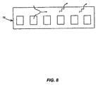
図6Aは、デバイス68の断面側面図であり、図6Bは、デバイス68の水平断面図である。上記デバイスは、GaNから構成された300nmのアクティブ層70を有しており、上記アクティブ層は、SiO2から構成されたパターニングまたは貫通または穿孔されたマスク74を含む300nmのパターニングされた層72の上に形成されている。上記マスクは、GaNから構成された5ミクロンのバッファ層76の上に堆積されており、上記バッファ層は、サファイアから構成された基板78の上に成長されている。パターニングされた層72は、主要なコンポーネントとしてSiO2のマスク74を用いており、放射モードおよび導波モードへのアクティブ層70の放出を制御する。このようにして、デバイス68は、パターニングされた層72の特定の設計を要求し、正確に成長された例えば量子井戸(QW)のような発光種80を含む薄いアクティブ層70を要求する。最大の効率が必要とされる場合、これらの発光種80は、アクティブ層70内に最適に配置され得る。
(Technical description)
FIG. 6A is a cross-sectional side view of the
そのような構造の直接的な利点は、成長マスクとしてパターニングされた層を用いることにより、アクティブ層がLEOによって成長される場合に、成長材料が、優れた光電性能を有するものになり得るということである(LEO成長に関する従来の研究から公知である)。図7は、GaN材料から構成されたLEO成長されたマイクロキャビティLEDの放出特性の簡略化されたシミュレーションを示している。300nmの薄いパターニングされた層は、表面の50%をカバーするパターニングされたSiO2のマスクと、マスク内のホールを充填するGaNとから構成されている。そして、公知な指標を用いることにより、空中に放出される光の一部、導光モードまたは漏れモードは、アクティブ層の厚さと、アクティブ層に配置された発光体(すなわち、QW)との関数として、計算され得る。簡略化されたシミュレーションは、そのような構造の上手く制御された放出特性を示している:光の15〜20%のみが漏れモードで放出されるが、このことは光の少なくとも80%が回収され得ることを意味している。 A direct advantage of such a structure is that by using a patterned layer as a growth mask, the growth material can have excellent photoelectric performance when the active layer is grown by LEO. (Known from previous studies on LEO growth). FIG. 7 shows a simplified simulation of the emission characteristics of a LEO grown microcavity LED constructed from GaN material. The 300 nm thin patterned layer is composed of a patterned SiO 2 mask covering 50% of the surface and GaN filling the holes in the mask. Then, by using a known index, a part of the light emitted into the air, the light guide mode or the leakage mode is a function of the thickness of the active layer and the light emitter (ie, QW) disposed in the active layer. Can be calculated as: A simplified simulation shows a well-controlled emission characteristic of such a structure: only 15-20% of the light is emitted in leaky mode, which means that at least 80% of the light is recovered That means getting.
図7にはまた、相対的な全放出率(relative total emission rate;パーセル効果)が示されている。効率およびパーセル効果は、SiO2の上部の上のGaN層の厚さ(横軸)と、SiO2層の上部に対するその層における放出量子井戸の相対的な位置(縦軸)とを対照して、グレースケールとしてプロットされている。 FIG. 7 also shows the relative total emission rate (parcel effect). Efficiency and the parcel effect contrasted with the thickness of the GaN layer above the top of SiO 2 (horizontal axis) and the relative position of the emitted quantum well in that layer relative to the top of the SiO 2 layer (vertical axis) , Plotted as grayscale.
光のほとんどが直接的または導波モードで放出される(すなわち、漏れモードが15%未満である)場所に、領域が見出され得(すなわち、層の厚さが270nm、QWがその値の70%に位置する)、直接抽出効率は、導波モードにおける発光の30%から55%の範囲にある。 A region can be found where most of the light is emitted directly or in a guided mode (ie, the leakage mode is less than 15%) (ie, the layer thickness is 270 nm, the QW is at that value) The direct extraction efficiency is in the range of 30% to 55% of the emission in the guided mode.
図8は、回折による導波モードの抽出を示しており、回折格子としてパターニングされた層72を用いている。シミュレーションは、80%範囲の抽出効率が可能であるということを示している。パターニングされたマスク内のホールのパターンおよびサイズに依存して、さらにはデバイス構造の上部または底部に配置される金属ミラーの使用にもまた依存して、デバイスの上部または底部に、放出が発生し得る。
FIG. 8 illustrates the extraction of guided modes by diffraction, using a patterned
パターニングされた層72のマスク74におけるパターン、穿孔、または貫通に関し、様々な幾何学的形状が用いられ得る。最も単純な幾何学的形状は、正方形または長方形の配列(例えば、いわゆる周期的なフォトニッククリスタル)であり、それぞれは、図9において、82および84として示されている。図9において86として示されているアルキメデスタイリングのような、より複雑な幾何学的形状もまた、より効率的な光抽出をもたらし得る。最後に、波長に近い特性相関長(characteristic correlation length)を有し得るいくぶんランダムなパターンもまた、効率的な光散乱体として機能し得る。
Various geometries can be used for the pattern, perforation, or penetration in the
薄膜マイクロキャビティの幾何学的形状でパターニングされた層72の上での成長に関するコンセプトについて、多くの可能なインプリメンテーションが存在する。例えば、図10に示されているように、2つのパターニングされた層72、2つのマスク74、および2つのLEO成長が、アクティブ層70の材料品質を向上させるために用いられ得る。
パターニングされた層72の回折によってマイクロキャビティ効果および抽出特性を保持するために、薄い成長(典型的には、200〜1000nmの厚さ)において、出来る限り良い材料を取得することに対する挑戦が存在する。
There are many possible implementations for the concept of growth on
There is a challenge to obtaining the best possible material in thin growth (typically 200-1000 nm thickness) to preserve the microcavity effect and extraction properties by diffraction of the patterned
金属または誘電性のミラーが、パターニングされた層72の上または下に(例えば、構造の上部、パターニングされた層72の下、または基板78の下に)配置され得、所望の方向の放出を向上または低減させ、漏れモードに放出された光の一部を基板78に向けて抽出する。
A metal or dielectric mirror can be placed above or below the patterned layer 72 (eg, above the structure, below the patterned
パターニングされた層72のマスク74は、絶縁性材料、半導性材料、または金属材料から構成され得る。パターニングされた層72のマスク74の屈折率が、アクティブ層70の屈折率、および/またはマスク74内のホールを充填する材料の屈折率から、十分に異なっていることが、要求される。
The
図11は、デバイスの断面側面図であり、アクティブ層70における2つの発光種80A、80B(すなわち、量子井戸)は、異なる波長で放出しており、パターニングされた層72におけるマスク74の2つのパターン88Aおよび88Bは、導波を放射モード90Aおよび90Bに変換している。ここで、90Aは80Aに関連しており、90Bは80Bに関連している。このようにして、異なる周期を有する、パターニングされた層72のマスク74における異なるパターン88A、88Bは、回折によって様々な波長で90A、90Bを抽出するために、用いられ得る。パターニングされた層72におけるマスク74のその他のパラメータは、空間的に変化され得(例えば、ホールの形状、マスク74および/またはパターニングされた層72のサイズまたは深さまたは厚さ)、結果として、構造の異なる領域におけるパターニングされた層72のマスク74に関し、異なる性質を有することができる。
FIG. 11 is a cross-sectional side view of the device, where the two light emitting
さらに、追加的なアクティブな光励起された領域が用いられ得、導波モードを再利用することにより、別の周波数で導波モードの一部を再放出する。例えば、そのような構造は、第1の量子井戸80の層が青色の波長で放出し、第2の量子井戸80の層が黄色の波長で放出する場合に、白色光を生成するために用いられ得る。追加的なアクティブ領域は、任意の種類の量子井戸のうちのいずれかであり得、InGaN(Zn:Si)、複数の量子ドット、複数の蛍光体、色素、重合体、または微粒子を含む。発光種の一部または全部は、電流注入され得る。 In addition, additional active photoexcited regions can be used to re-emit part of the guided mode at another frequency by reusing the guided mode. For example, such a structure can be used to generate white light when the first quantum well 80 layer emits at a blue wavelength and the second quantum well 80 layer emits at a yellow wavelength. Can be. The additional active region may be any of any type of quantum well and includes InGaN (Zn: Si), multiple quantum dots, multiple phosphors, dyes, polymers, or microparticles. Some or all of the luminescent species can be current injected.
別のアーキテクチャは、LED構造の周辺で分離した放出ゾーンと抽出ゾーンとを有しているLEDを提供する。図12は、LED92の断面側面図であり、分離した放出領域94と回折領域96,98とを有している。
Another architecture provides an LED having an emission zone and an extraction zone separated around the LED structure. FIG. 12 is a cross-sectional side view of the
本発明の変形は、上部における金属ミラーを含み得、上記ミラーは、放出が発生する基板を保持する。あるいは、基板のリフトオフ技術を用いるときには、基板を用いない。図13は、LED100の断面側面図であり、分離した放出領域104と回折領域104,106とを有している。ここで、LED100は、基板を含んでいないが、金属の裏面接触108を有している。
Variations of the invention can include a metal mirror at the top, which holds the substrate on which the emission occurs. Alternatively, the substrate is not used when the substrate lift-off technique is used. FIG. 13 is a cross-sectional side view of the
本発明はまた、非常に指向性が高い光源としても機能し得、放出は主に、導波モードの構造の適切な調整により、特定の方向で発生し、その結果、指向性LEDを生成する。上記構造の設計が正しい場合、わずか数個の(理想的には1つの)導波モードが励起され、その後、回折格子によって抽出される。この場合では、各導波モードは正しく定義された角度(これは、回折格子のパラメータを調整することによって選択される)で回折されるので、狭い範囲の方向で発光が発生する。 The present invention can also function as a highly directional light source, where emission occurs mainly in a specific direction by appropriate adjustment of the guided mode structure, resulting in a directional LED . If the structure design is correct, only a few (ideally one) guided modes are excited and then extracted by the diffraction grating. In this case, each guided mode is diffracted at a correctly defined angle (which is selected by adjusting the parameters of the diffraction grating), so that light emission occurs in a narrow range of directions.
図14は、LED110の断面側面図を示しており、分離した放出領域112と回折領域114,116とを有している。ここで、LED110は、上部の金属ミラー118と、底部の粗くされた表面120とを含んでおり、不規則的に補助された抽出を提供する。漏れモードを抽出するために、デバイス110の裏面の粗くされた表面120が用いられ得る。粗くされた表面120は、裏面全体または裏面の一部を(例えば、その周辺において)含んでいる。
FIG. 14 shows a cross-sectional side view of the
窒化物LEDに関連して記載されてきたが、この高性能のLEDの枠組みは、そのような製造技術を受け入れる任意の材料に適用され得る:それは、半導体であり得るが、重合体または有機分子でもあり得る。後者の場合、幅広い発光種が使用されると仮定すると、適切な回折周期を有する特定の回折領域を用いることにより、高性能の白色発光を予見することができ、所与の色の光を放出することができる(さらに、その他の色に対し、キャビティを反共振にすることにより、それらの色での直接放出を抑制することもできる)。あるいは、単色の放出格子を局所アドレス指定に関連付けることにより、単一の重合体を混合したフルカラーディスプレイを得ることができる。 Although described in connection with nitride LEDs, this high-performance LED framework can be applied to any material that accepts such manufacturing techniques: it can be a semiconductor, but a polymer or organic molecule But it can be. In the latter case, assuming that a wide range of luminescent species is used, by using a specific diffractive region with an appropriate diffraction period, high performance white emission can be foreseen and emit light of a given color (Furthermore, direct emission in those colors can be suppressed by making the cavity anti-resonant for other colors). Alternatively, a full color display mixed with a single polymer can be obtained by associating a monochromatic emission grid with local addressing.
図15は、本発明の好適な実施形態にしたがう、LEDの断面側面図であり、2つのアクティブ領域122および124が、パターニングされた層126,128および130の間に配置されている。これらの場合、分離した導波モード132および134が、各アクティブ領域122および124内に存在し、その結果、パターニングされた層126,128および130は、モード132および134の一部で優先的に機能し得る。これは、例えば、2つのアクティブ領域122および124の発光種が異なる波長を放出する(例えば、この場合では格子が各波長に対して最適化される)場合に、有用であり得る。
FIG. 15 is a cross-sectional side view of an LED according to a preferred embodiment of the present invention in which two
最後に、図16は、本発明の好適な実施形態にしたがって実行される、製造ステップを示すフローチャートである。 Finally, FIG. 16 is a flowchart illustrating the manufacturing steps performed in accordance with the preferred embodiment of the present invention.
ブロック136は、基板上にバッファ層を成長させるステップを示しており、上記バッファ層は、GaNベースの材料である。
ブロック138は、LEOを用いてバッファ層の上部に1つ以上のパターニングされた層を成長させるステップを示しており、各パターニングされた層は、マスクと該マスク内のホールを充填する材料とを含んでいる。好適には、上記マスクは、絶縁性材料、半導性材料、または金属材料から構成され、マスク内のホールを充填する材料は、LEOによって成長されたGaNベースの材料を含んでいる。パターニングされた層は、アクティブ層との屈折率のコントラストに起因して、光閉じ込め層として機能するか、あるいはマスクと上記マスク内のホールを充填する材料との間の屈折率の変化に起因して、埋め込み回折格子として機能する。パターニングされた層において、異なるパターンが用いられ、回折によって異なる波長を抽出するか、あるいは回折の方向を変化させる。
ブロック140は、パターニングされた層の上またはパターニングされた層の間に、1つ以上のアクティブ層を形成するステップを示しており、上記アクティブ層は、GaNベースの材料であり、1つ以上の発光種を含んでいる。好適には、アクティブ層は、LEOによって成長される。
これらのステップの最終結果は、LED(アクティブ層との屈折率のコントラストに起因して、光閉じ込め層として機能し、かつ/またはマスクと上記マスク内のホールを充填する材料との間の屈折率の変化に起因して、埋め込み回折格子として機能する)である。 The end result of these steps is that the refractive index between the LED (which acts as a light confinement layer and / or fills the holes in the mask due to the refractive index contrast with the active layer) (Because it changes as a buried diffraction grating).
(文献)
以下の文献は、参考のために本明細書に援用される。
(Reference)
The following documents are hereby incorporated by reference:
1.米国特許第6,538,371号、2003年3月25日公布、Duggal他、題名「White light illumination system with improved color ouput」
2.米国特許第6,525,464号、2003年2月25日公布、Chin、題名「Stacked light−mixing LED」
3.米国特許第6,504,180号、2003年1月7日公布、Heremans他、題名「Method of manufacturing surface textured high−effeciency radiating devices and devices obtained therefrom」
4.米国特許第6,163,038号、2000年12月19日公布、Chen他、題名「White light−emitting diode and method of manufacturing the same」
5.米国特許第5,779,924号、1998年7月14日公布、Krames他、題名「Ordered interface texturing for a light emitting device」
6.米国特許第5,362,977号、1994年11月8日公布、Hunt他、題名「Single mirror light−emitting diodes with enhanced intensity」
7.米国特許第5,226,053号、1993年7月6日公布、Cho他、題名「Light emitting diode」
8.Shnitzer他、「30% External Quantum Efficiency From Surface Textured、Thin Film Light Emitting Diode」、Applied Physics Letters 63、pp.2174−2176、1993
9.M.Boroditsky、E.Yablonovtich、「Light extraction efficiency from light−emitting diodes」、Proceedigs of the SPIE−The International Society for Optical Engineering、SPIE−Int.Soc.Opt.Eng.、3002、pp.119−122、1997
10.H.Bensity、H.D.Neve、およびC.Weisbuch、「Impact of planar microcavity effects on light extraction/Basic concepts and analytical trends」、IEEE J.Quantumn Electron、vol.34、p.1612(1998)
11.D.Delbeke、R.Bockstaele、P.Bienstman、R.Baets、およびH.Benisty、「High−efficiency Semiconductor Resonant−Cavity Light−Emitting diodes:A Review」、IEEE J.on selected topics in Quantum Electron、vol.8、no.2、p.189、2002
12.M.Rattier、H.Benisty、E.Schwoob、C.Weisbuch、T.Krauss、C.J.M.Smith、R.Houdre、およびU.Oesterle、「Omnidirectional and compact light extraction from Archimedean photonic lattices」、Appl.Phys.Lett.83、1283、2003
13.M.Rattier、H.Benisty、R.Stanley、J.F.Carlin、R.Houdre、U.Oesterle、C.J.M.Smith、C.Weisbuch、およびT.Krauss、「Toward ultrahigh−efficiency aluminum oxide microcavity light−emitting diodes:Guided mode extraction by photonic crystals」、IEEE Sel.Top.Quantum Electr.8、238、2002
(結論)
本発明の好適な実施形態の記載を終了する。本発明の1つ以上の実施形態に関する上述の記載は、例示および記載を目的として、示されてきた。網羅的であること、あるいは本発明を開示された形に限定することは、意図されていない。上述の教示を踏まえると、多くの改変およびバリエーションが可能である。本発明の範囲は、この詳細な説明によってではなくむしろ、本明細書に添付された請求の範囲によって限定されることが、意図されている。
1. US Pat. No. 6,538,371, promulgated on March 25, 2003, Dogal et al., Entitled “White light illumination system with improved color output”
2. US Pat. No. 6,525,464, promulgated on Feb. 25, 2003, Chin, entitled “Stacked light-mixing LED”
3. U.S. Pat. No. 6,504,180, promulgated on Jan. 7, 2003, Heremans et al., Title "Method of manufacturing surface textured high-efficiency radiating devices and devices objeted."
4). US Pat. No. 6,163,038, promulgated on December 19, 2000, Chen et al., Entitled “White light-emitting diode and method of manufacturing the same”
5. US Pat. No. 5,779,924, promulgated July 14, 1998, Krames et al., Entitled “Ordered interface texturing for a light emitting device”.
6). US Pat. No. 5,362,977, promulgated on November 8, 1994, Hunt et al., Entitled “Single mirror light-emitting diodes with enhanced intensity”
7). US Pat. No. 5,226,053, promulgated on July 6, 1993, Cho et al., Entitled “Light emitting diode”
8). Schnitzer et al., “30% External Quantum Efficiency Surface Textured, Thin Film Light Emitting Diode”, Applied Physics Letters 63, pp. 2174-2176, 1993
9. M.M. Boroditsky, E .; Yablonovich, “Light extraction efficiency light-emitting diodes”, Proceedings of the SPIE-The International Society for Optical In-Pig. Soc. Opt. Eng. , 3002, pp. 119-122, 1997
10. H. Bensity, H.C. D. Neve, and C.I. Weisbuch, “Impact of planar microcavity effects on light extraction / Basic concepts and analytical trends”, IEEE J. Biol. Quantum Electron, vol. 34, p. 1612 (1998)
11. D. Delbeke, R.D. Bockstaele, P.M. Bienstman, R.M. Baets, and H.C. Benisty, “High-Efficiency Semiconductor Resonant-Cavity Light-Emitting Diodes: A Review”, IEEE J. MoI. on selected topics in Quantum Electron, vol. 8, no. 2, p. 189, 2002
12 M.M. Rattier, H.C. Benisty, E.M. Schwobu, C.I. Weisbuch, T .; Krauss, C.I. J. et al. M.M. Smith, R.A. Houdre, and U.I. Osterle, “Omnidirectional and compact light extraction form Archimedean photonic lattices”, Appl. Phys. Lett. 83, 1283, 2003
13. M.M. Rattier, H.C. Benisty, R.A. Stanley, J.M. F. Carlin, R.C. Houdre, U.S.A. Osterle, C.I. J. et al. M.M. Smith, C.I. Weisbuch, and T.W. Krauss, “Toward ultrahigh-efficiency aluminum oxide microcavity light-emitting diodes: Guided mode extraction by photonic crystals E. Estr. Top. Quantum Electr. 8, 238, 2002
(Conclusion)
The description of the preferred embodiment of the present invention ends. The foregoing description of one or more embodiments of the invention has been presented for purposes of illustration and description. It is not intended to be exhaustive or to limit the invention to the form disclosed. Many modifications and variations are possible in light of the above teaching. It is intended that the scope of the invention be limited not by this detailed description, but rather by the claims appended hereto.
ここで図面を参照すると、図中では、複数の図面を通して、同様の参照番号は、対応する部分を表している。
Claims (33)
(a)1つ以上のパターニングされた層であって、各パターニングされた層は、マスクおよび該マスク内のホールを充填する材料を含んでいる、パターニングされた層と、
(b)該パターニングされた層の上または該パターニングされた層の間に形成された1つ以上のアクティブ層であって、該アクティブ層は、1つ以上の発光種を含んでいる、アクティブ層と
を備えており、
(c)各パターニングされた層は、該アクティブ層の該発光種に対し、光閉じ込め層または埋め込み回折格子として機能する、LED。 A light emitting diode (LED),
(A) one or more patterned layers, each patterned layer comprising a mask and a material that fills holes in the mask;
(B) one or more active layers formed on or between the patterned layers, the active layers comprising one or more luminescent species And
(C) Each patterned layer functions as a light confinement layer or buried diffraction grating for the luminescent species of the active layer.
(a)1つ以上のパターニングされた層を堆積することであって、各パターニングされた層は、マスクおよび該マスク内のホールを充填する材料を含んでいる、ことと、
(b)該パターニングされた層の上または該パターニングされた層の間に1つ以上のアクティブ層を形成することであって、該アクティブ層は、1つ以上の発光種を含んでいる、ことと
を包含し、
(c)該パターニングされた層は、該アクティブ層の該発光種に対し、光閉じ込め層または埋め込み回折格子として機能する、方法。 A method of manufacturing a light emitting diode (LED) comprising:
(A) depositing one or more patterned layers, each patterned layer comprising a mask and a material filling the holes in the mask;
(B) forming one or more active layers on or between the patterned layers, wherein the active layers include one or more luminescent species; And
(C) The method wherein the patterned layer functions as a light confinement layer or a buried diffraction grating for the luminescent species of the active layer.
Applications Claiming Priority (2)
| Application Number | Priority Date | Filing Date | Title |
|---|---|---|---|
| US11/067,910 US7291864B2 (en) | 2005-02-28 | 2005-02-28 | Single or multi-color high efficiency light emitting diode (LED) by growth over a patterned substrate |
| PCT/US2006/007029 WO2006093937A2 (en) | 2005-02-28 | 2006-02-28 | Single or multi-color high efficiency light emitting diode (led) by growth over a patterned substrate |
Related Child Applications (2)
| Application Number | Title | Priority Date | Filing Date |
|---|---|---|---|
| JP2012024680A Division JP2012114458A (en) | 2005-02-28 | 2012-02-08 | Single or multi-color high efficiency light emitting diode (led) by growth over patterned substrate |
| JP2012024681A Division JP2012119717A (en) | 2005-02-28 | 2012-02-08 | Single or multi-color high efficiency light emitting diode (led) by growth over patterned substrate |
Publications (2)
| Publication Number | Publication Date |
|---|---|
| JP2008536294A true JP2008536294A (en) | 2008-09-04 |
| JP2008536294A5 JP2008536294A5 (en) | 2009-04-16 |
Family
ID=36941725
Family Applications (3)
| Application Number | Title | Priority Date | Filing Date |
|---|---|---|---|
| JP2007558124A Pending JP2008536294A (en) | 2005-02-28 | 2006-02-28 | High performance light emitting diodes (LEDs), monochromatic or multicolored, grown on patterned substrates |
| JP2012024681A Withdrawn JP2012119717A (en) | 2005-02-28 | 2012-02-08 | Single or multi-color high efficiency light emitting diode (led) by growth over patterned substrate |
| JP2012024680A Withdrawn JP2012114458A (en) | 2005-02-28 | 2012-02-08 | Single or multi-color high efficiency light emitting diode (led) by growth over patterned substrate |
Family Applications After (2)
| Application Number | Title | Priority Date | Filing Date |
|---|---|---|---|
| JP2012024681A Withdrawn JP2012119717A (en) | 2005-02-28 | 2012-02-08 | Single or multi-color high efficiency light emitting diode (led) by growth over patterned substrate |
| JP2012024680A Withdrawn JP2012114458A (en) | 2005-02-28 | 2012-02-08 | Single or multi-color high efficiency light emitting diode (led) by growth over patterned substrate |
Country Status (5)
| Country | Link |
|---|---|
| US (3) | US7291864B2 (en) |
| EP (1) | EP1854156A2 (en) |
| JP (3) | JP2008536294A (en) |
| KR (1) | KR20070107799A (en) |
| WO (1) | WO2006093937A2 (en) |
Cited By (6)
| Publication number | Priority date | Publication date | Assignee | Title |
|---|---|---|---|---|
| JP2007214576A (en) * | 2006-02-10 | 2007-08-23 | Samsung Electro Mech Co Ltd | Nitride semiconductor light-emitting device and manufacturing method therefor |
| JP2013529846A (en) * | 2010-06-24 | 2013-07-22 | ソウル オプト デバイス カンパニー リミテッド | Light emitting diode |
| JP2013540335A (en) * | 2010-10-08 | 2013-10-31 | ガーディアン・インダストリーズ・コーポレーション | Light source having light scattering feature, apparatus including light source having light scattering feature, and / or manufacturing method thereof |
| US8907360B2 (en) | 2009-11-13 | 2014-12-09 | Seoul Viosys Co., Ltd. | Light emitting diode chip having distributed bragg reflector, method of fabricating the same, and light emitting diode package having distributed bragg reflector |
| US8963178B2 (en) | 2009-11-13 | 2015-02-24 | Seoul Viosys Co., Ltd. | Light emitting diode chip having distributed bragg reflector and method of fabricating the same |
| US8963183B2 (en) | 2010-07-28 | 2015-02-24 | Seoul Viosys Co., Ltd. | Light emitting diode having distributed Bragg reflector |
Families Citing this family (38)
| Publication number | Priority date | Publication date | Assignee | Title |
|---|---|---|---|---|
| DE60341314C5 (en) * | 2003-12-09 | 2023-03-23 | The Regents Of The University Of California | HIGH EFFICIENCY GALLIUM NITRIDE BASED GALLIUM NITRIDE LIGHT Emitting Emitters With roughened surface |
| US7768023B2 (en) * | 2005-10-14 | 2010-08-03 | The Regents Of The University Of California | Photonic structures for efficient light extraction and conversion in multi-color light emitting devices |
| US8227820B2 (en) | 2005-02-09 | 2012-07-24 | The Regents Of The University Of California | Semiconductor light-emitting device |
| US8294166B2 (en) | 2006-12-11 | 2012-10-23 | The Regents Of The University Of California | Transparent light emitting diodes |
| US8860051B2 (en) | 2006-11-15 | 2014-10-14 | The Regents Of The University Of California | Textured phosphor conversion layer light emitting diode |
| US7582910B2 (en) * | 2005-02-28 | 2009-09-01 | The Regents Of The University Of California | High efficiency light emitting diode (LED) with optimized photonic crystal extractor |
| US7345298B2 (en) | 2005-02-28 | 2008-03-18 | The Regents Of The University Of California | Horizontal emitting, vertical emitting, beam shaped, distributed feedback (DFB) lasers by growth over a patterned substrate |
| US7772607B2 (en) * | 2004-09-27 | 2010-08-10 | Supernova Optoelectronics Corporation | GaN-series light emitting diode with high light efficiency |
| US7291864B2 (en) * | 2005-02-28 | 2007-11-06 | The Regents Of The University Of California | Single or multi-color high efficiency light emitting diode (LED) by growth over a patterned substrate |
| US8163575B2 (en) * | 2005-06-17 | 2012-04-24 | Philips Lumileds Lighting Company Llc | Grown photonic crystals in semiconductor light emitting devices |
| EP1908125A2 (en) * | 2005-06-17 | 2008-04-09 | The Regents of the University of California | (AI,Ga,In)N AND ZnO DIRECT WAFER BONDED STRUCTURE FOR OPTOELECTRONIC APPLICATION AND ITS FABRICATION METHOD |
| US20070096127A1 (en) * | 2005-08-26 | 2007-05-03 | Pattison P M | Semiconductor micro-cavity light emitting diode |
| JP5096671B2 (en) * | 2005-09-13 | 2012-12-12 | 日立マクセルエナジー株式会社 | Sealed prismatic battery |
| JP2009515344A (en) * | 2005-11-04 | 2009-04-09 | ザ リージェンツ オブ ザ ユニバーシティ オブ カリフォルニア | Light-emitting diode (LED) with high light extraction efficiency |
| WO2007065005A2 (en) * | 2005-12-02 | 2007-06-07 | The Regents Of University Of California | Improved horizontal emitting, vertical emitting, beam shaped, distributed feedback (dfb) lasers fabricated by growth over a patterned substrate with multiple overgrowth |
| WO2007067758A2 (en) * | 2005-12-08 | 2007-06-14 | The Regents Of The University Of California | High efficiency light emitting diode (led) |
| DE102006046037A1 (en) * | 2006-09-28 | 2008-04-03 | Osram Opto Semiconductors Gmbh | Light emitting diode semiconductor body for radiation-emitting component and for applications of projection, has radiation generating active layers and photonic crystal |
| WO2008042337A2 (en) * | 2006-09-28 | 2008-04-10 | Memon Vinod M | Spin-coated polymer microcavity for light emitters and lasers |
| US7934194B2 (en) | 2006-10-17 | 2011-04-26 | The Mathworks, Inc. | User-defined hierarchies of user-defined classes of graphical objects in a graphical modeling environment |
| JP5372766B2 (en) * | 2006-11-15 | 2013-12-18 | ザ リージェンツ オブ ザ ユニバーシティ オブ カリフォルニア | Spherical LED with high light extraction efficiency |
| US20090121250A1 (en) * | 2006-11-15 | 2009-05-14 | Denbaars Steven P | High light extraction efficiency light emitting diode (led) using glass packaging |
| TW200830593A (en) * | 2006-11-15 | 2008-07-16 | Univ California | Transparent mirrorless light emitting diode |
| JP2010512660A (en) * | 2006-12-11 | 2010-04-22 | ザ リージェンツ オブ ザ ユニバーシティ オブ カリフォルニア | Nonpolar and semipolar light emitting devices |
| TWI533351B (en) | 2006-12-11 | 2016-05-11 | 美國加利福尼亞大學董事會 | Metalorganic chemical vapor deposition (mocvd) growth of high performance non-polar iii-nitride optical devices |
| DE102007003785A1 (en) * | 2007-01-19 | 2008-07-24 | Merck Patent Gmbh | Emitter converter chip |
| DE102007062041B4 (en) * | 2007-09-28 | 2021-10-21 | OSRAM Opto Semiconductors Gesellschaft mit beschränkter Haftung | Polarized radiation emitting semiconductor chip |
| TWI389346B (en) * | 2008-10-01 | 2013-03-11 | Epistar Corp | Opto-electronic device |
| TW201123537A (en) * | 2009-08-28 | 2011-07-01 | Univ California | Light emitting devices with embedded void-gap structures through bonding of structured materials on active devices |
| US20110077994A1 (en) * | 2009-09-30 | 2011-03-31 | International Business Machines Corporation | Optimization of workforce scheduling and capacity planning |
| KR101631599B1 (en) * | 2009-12-02 | 2016-06-27 | 삼성전자주식회사 | Light Emitting Device and method for manufacturing the same |
| US8357553B2 (en) | 2010-10-08 | 2013-01-22 | Guardian Industries Corp. | Light source with hybrid coating, device including light source with hybrid coating, and/or methods of making the same |
| DE102011012925A1 (en) * | 2011-03-03 | 2012-09-06 | Osram Opto Semiconductors Gmbh | Method for producing an optoelectronic semiconductor chip |
| US20130001597A1 (en) * | 2011-06-28 | 2013-01-03 | Osram Sylvania Inc. | Lighting Device Having a Color Tunable Wavelength Converter |
| WO2013152231A1 (en) * | 2012-04-04 | 2013-10-10 | The Regents Of The University Of California | Light emitting devices with embedded void-gap structures through techniques of closure of voids |
| WO2017175201A2 (en) * | 2016-04-08 | 2017-10-12 | Novagan | Low etendue high brightness light emitting devices |
| US10862002B2 (en) | 2018-04-27 | 2020-12-08 | Facebook Technologies, Llc | LED surface modification with ultraviolet laser |
| US11592166B2 (en) | 2020-05-12 | 2023-02-28 | Feit Electric Company, Inc. | Light emitting device having improved illumination and manufacturing flexibility |
| US11876042B2 (en) | 2020-08-03 | 2024-01-16 | Feit Electric Company, Inc. | Omnidirectional flexible light emitting device |
Citations (6)
| Publication number | Priority date | Publication date | Assignee | Title |
|---|---|---|---|---|
| JPH04167484A (en) * | 1990-10-31 | 1992-06-15 | Toshiba Corp | Photo-semiconductor device |
| JPH08204227A (en) * | 1995-01-20 | 1996-08-09 | Oki Electric Ind Co Ltd | Optical semiconductor element and optical communication unit |
| JPH11274642A (en) * | 1998-03-19 | 1999-10-08 | Toshiba Corp | Semiconductor light emitting element and fabrication thereof |
| JPH11274558A (en) * | 1998-03-23 | 1999-10-08 | Toshiba Corp | Semiconductor light emitting element and semiconductor light emitting device |
| JP2000021789A (en) * | 1997-08-29 | 2000-01-21 | Toshiba Corp | Nitride semiconductor element, light emitting element and their manufacture |
| WO2006062084A1 (en) * | 2004-12-08 | 2006-06-15 | Sumitomo Electric Industries, Ltd. | Semiconductor laser device and method for manufacturing same |
Family Cites Families (24)
| Publication number | Priority date | Publication date | Assignee | Title |
|---|---|---|---|---|
| DE4135813C2 (en) * | 1990-10-31 | 1997-11-06 | Toshiba Kawasaki Kk | Semiconductor surface emitting laser device |
| US5226053A (en) * | 1991-12-27 | 1993-07-06 | At&T Bell Laboratories | Light emitting diode |
| US5362977A (en) * | 1992-12-28 | 1994-11-08 | At&T Bell Laboratories | Single mirror light-emitting diodes with enhanced intensity |
| JPH07326820A (en) * | 1994-05-30 | 1995-12-12 | Mitsubishi Electric Corp | Variable wavelength semiconductor laser device |
| US5779924A (en) * | 1996-03-22 | 1998-07-14 | Hewlett-Packard Company | Ordered interface texturing for a light emitting device |
| US5771256A (en) * | 1996-06-03 | 1998-06-23 | Bell Communications Research, Inc. | InP-based lasers with reduced blue shifts |
| JPH11135838A (en) * | 1997-10-20 | 1999-05-21 | Ind Technol Res Inst | White-color light-emitting diode and manufacture thereof |
| US6086673A (en) * | 1998-04-02 | 2000-07-11 | Massachusetts Institute Of Technology | Process for producing high-quality III-V nitride substrates |
| JP3559453B2 (en) * | 1998-06-29 | 2004-09-02 | 株式会社東芝 | Light emitting element |
| US6504180B1 (en) * | 1998-07-28 | 2003-01-07 | Imec Vzw And Vrije Universiteit | Method of manufacturing surface textured high-efficiency radiating devices and devices obtained therefrom |
| US6657236B1 (en) * | 1999-12-03 | 2003-12-02 | Cree Lighting Company | Enhanced light extraction in LEDs through the use of internal and external optical elements |
| JP2001177145A (en) * | 1999-12-21 | 2001-06-29 | Toshiba Electronic Engineering Corp | Semiconductor light emitting device and method of manufacturing the same |
| US6538371B1 (en) * | 2000-03-27 | 2003-03-25 | The General Electric Company | White light illumination system with improved color output |
| US6525464B1 (en) * | 2000-09-08 | 2003-02-25 | Unity Opto Technology Co., Ltd. | Stacked light-mixing LED |
| JP2003069145A (en) * | 2001-06-14 | 2003-03-07 | Furukawa Electric Co Ltd:The | Method of manufacturing distributed feedback semiconductor laser element group |
| US6740906B2 (en) * | 2001-07-23 | 2004-05-25 | Cree, Inc. | Light emitting diodes including modifications for submount bonding |
| US6903379B2 (en) * | 2001-11-16 | 2005-06-07 | Gelcore Llc | GaN based LED lighting extraction efficiency using digital diffractive phase grating |
| JP3782357B2 (en) * | 2002-01-18 | 2006-06-07 | 株式会社東芝 | Manufacturing method of semiconductor light emitting device |
| US7098589B2 (en) * | 2003-04-15 | 2006-08-29 | Luminus Devices, Inc. | Light emitting devices with high light collimation |
| US7012279B2 (en) * | 2003-10-21 | 2006-03-14 | Lumileds Lighting U.S., Llc | Photonic crystal light emitting device |
| US7808011B2 (en) * | 2004-03-19 | 2010-10-05 | Koninklijke Philips Electronics N.V. | Semiconductor light emitting devices including in-plane light emitting layers |
| US7345298B2 (en) * | 2005-02-28 | 2008-03-18 | The Regents Of The University Of California | Horizontal emitting, vertical emitting, beam shaped, distributed feedback (DFB) lasers by growth over a patterned substrate |
| US7223998B2 (en) * | 2004-09-10 | 2007-05-29 | The Regents Of The University Of California | White, single or multi-color light emitting diodes by recycling guided modes |
| US7291864B2 (en) * | 2005-02-28 | 2007-11-06 | The Regents Of The University Of California | Single or multi-color high efficiency light emitting diode (LED) by growth over a patterned substrate |
-
2005
- 2005-02-28 US US11/067,910 patent/US7291864B2/en not_active Expired - Fee Related
-
2006
- 2006-02-28 WO PCT/US2006/007029 patent/WO2006093937A2/en active Application Filing
- 2006-02-28 EP EP06736368A patent/EP1854156A2/en not_active Withdrawn
- 2006-02-28 KR KR1020077022109A patent/KR20070107799A/en not_active Application Discontinuation
- 2006-02-28 JP JP2007558124A patent/JP2008536294A/en active Pending
-
2007
- 2007-10-24 US US11/923,414 patent/US7755096B2/en not_active Expired - Fee Related
-
2010
- 2010-06-04 US US12/793,862 patent/US8390011B2/en active Active
-
2012
- 2012-02-08 JP JP2012024681A patent/JP2012119717A/en not_active Withdrawn
- 2012-02-08 JP JP2012024680A patent/JP2012114458A/en not_active Withdrawn
Patent Citations (6)
| Publication number | Priority date | Publication date | Assignee | Title |
|---|---|---|---|---|
| JPH04167484A (en) * | 1990-10-31 | 1992-06-15 | Toshiba Corp | Photo-semiconductor device |
| JPH08204227A (en) * | 1995-01-20 | 1996-08-09 | Oki Electric Ind Co Ltd | Optical semiconductor element and optical communication unit |
| JP2000021789A (en) * | 1997-08-29 | 2000-01-21 | Toshiba Corp | Nitride semiconductor element, light emitting element and their manufacture |
| JPH11274642A (en) * | 1998-03-19 | 1999-10-08 | Toshiba Corp | Semiconductor light emitting element and fabrication thereof |
| JPH11274558A (en) * | 1998-03-23 | 1999-10-08 | Toshiba Corp | Semiconductor light emitting element and semiconductor light emitting device |
| WO2006062084A1 (en) * | 2004-12-08 | 2006-06-15 | Sumitomo Electric Industries, Ltd. | Semiconductor laser device and method for manufacturing same |
Cited By (13)
| Publication number | Priority date | Publication date | Assignee | Title |
|---|---|---|---|---|
| US8183068B2 (en) | 2006-02-10 | 2012-05-22 | Samsung Electro-Mechanics Co., Ltd. | Nitride-based semiconductor light emitting device and method of manufacturing the same |
| JP2007214576A (en) * | 2006-02-10 | 2007-08-23 | Samsung Electro Mech Co Ltd | Nitride semiconductor light-emitting device and manufacturing method therefor |
| US10128306B2 (en) | 2009-11-13 | 2018-11-13 | Seoul Viosys Co., Ltd. | Light emitting diode chip having distributed bragg reflector and method of fabricating the same |
| US10141480B2 (en) | 2009-11-13 | 2018-11-27 | Seoul Viosys Co., Ltd. | Light emitting diode chip having distributed Bragg reflector and method of fabricating the same |
| US8907360B2 (en) | 2009-11-13 | 2014-12-09 | Seoul Viosys Co., Ltd. | Light emitting diode chip having distributed bragg reflector, method of fabricating the same, and light emitting diode package having distributed bragg reflector |
| US8963178B2 (en) | 2009-11-13 | 2015-02-24 | Seoul Viosys Co., Ltd. | Light emitting diode chip having distributed bragg reflector and method of fabricating the same |
| US9324919B2 (en) | 2009-11-13 | 2016-04-26 | Seoul Viosys Co., Ltd. | Light emitting diode chip having distributed Bragg reflector and method of fabricating the same |
| US9343631B2 (en) | 2009-11-13 | 2016-05-17 | Seoul Viosys Co., Ltd. | Light emitting diode chip having distributed bragg reflector and method of fabricating the same |
| US9577157B2 (en) | 2009-11-13 | 2017-02-21 | Seoul Viosys Co., Ltd. | Light emitting diode chip having distributed Bragg reflector and method of fabricating the same |
| JP2013529846A (en) * | 2010-06-24 | 2013-07-22 | ソウル オプト デバイス カンパニー リミテッド | Light emitting diode |
| US9142715B2 (en) | 2010-06-24 | 2015-09-22 | Seoul Viosys Co., Ltd. | Light emitting diode |
| US8963183B2 (en) | 2010-07-28 | 2015-02-24 | Seoul Viosys Co., Ltd. | Light emitting diode having distributed Bragg reflector |
| JP2013540335A (en) * | 2010-10-08 | 2013-10-31 | ガーディアン・インダストリーズ・コーポレーション | Light source having light scattering feature, apparatus including light source having light scattering feature, and / or manufacturing method thereof |
Also Published As
| Publication number | Publication date |
|---|---|
| EP1854156A2 (en) | 2007-11-14 |
| US20060202226A1 (en) | 2006-09-14 |
| US20080087909A1 (en) | 2008-04-17 |
| JP2012114458A (en) | 2012-06-14 |
| WO2006093937A3 (en) | 2009-04-09 |
| US8390011B2 (en) | 2013-03-05 |
| US7755096B2 (en) | 2010-07-13 |
| WO2006093937A2 (en) | 2006-09-08 |
| US20100295081A1 (en) | 2010-11-25 |
| KR20070107799A (en) | 2007-11-07 |
| JP2012119717A (en) | 2012-06-21 |
| US7291864B2 (en) | 2007-11-06 |
Similar Documents
| Publication | Publication Date | Title |
|---|---|---|
| US7755096B2 (en) | Single or multi-color high efficiency light emitting diode (LED) by growth over a patterned substrate | |
| US7776629B2 (en) | High efficiency light emitting diode (LED) with optimized photonic crystal extractor | |
| US7223998B2 (en) | White, single or multi-color light emitting diodes by recycling guided modes | |
| US7768023B2 (en) | Photonic structures for efficient light extraction and conversion in multi-color light emitting devices | |
| US7504669B2 (en) | Light emitting devices | |
| JP5237286B2 (en) | Light emitting device comprising an array of emitters defined by a photonic crystal | |
| TWI330856B (en) | Light emitting devices(7) | |
| US20080121917A1 (en) | High efficiency white, single or multi-color light emitting diodes (leds) by index matching structures | |
| JP5289448B2 (en) | Semiconductor body for radiation emission | |
| JP4263121B2 (en) | LIGHT EMITTING ELEMENT AND LIGHTING DEVICE | |
| Gessmann et al. | Light-emitting diodes with integrated omnidirectionally reflective contacts | |
| Lee et al. | Improvement in light-output efficiency of AlGaInP LEDs fabricated on stripe patterned epitaxy | |
| Pathak et al. | Improvement of Extraction Efficiency of LEDs using Photonic Structures |
Legal Events
| Date | Code | Title | Description |
|---|---|---|---|
| A521 | Written amendment |
Free format text: JAPANESE INTERMEDIATE CODE: A523 Effective date: 20090210 |
|
| A621 | Written request for application examination |
Free format text: JAPANESE INTERMEDIATE CODE: A621 Effective date: 20090210 |
|
| A521 | Written amendment |
Free format text: JAPANESE INTERMEDIATE CODE: A523 Effective date: 20090313 |
|
| A131 | Notification of reasons for refusal |
Free format text: JAPANESE INTERMEDIATE CODE: A131 Effective date: 20110809 |
|
| A977 | Report on retrieval |
Free format text: JAPANESE INTERMEDIATE CODE: A971007 Effective date: 20110810 |
|
| A601 | Written request for extension of time |
Free format text: JAPANESE INTERMEDIATE CODE: A601 Effective date: 20111108 |
|
| A602 | Written permission of extension of time |
Free format text: JAPANESE INTERMEDIATE CODE: A602 Effective date: 20111115 |
|
| A601 | Written request for extension of time |
Free format text: JAPANESE INTERMEDIATE CODE: A601 Effective date: 20111129 |
|
| A602 | Written permission of extension of time |
Free format text: JAPANESE INTERMEDIATE CODE: A602 Effective date: 20111206 |
|
| A601 | Written request for extension of time |
Free format text: JAPANESE INTERMEDIATE CODE: A601 Effective date: 20120105 |
|
| A602 | Written permission of extension of time |
Free format text: JAPANESE INTERMEDIATE CODE: A602 Effective date: 20120113 |
|
| A02 | Decision of refusal |
Free format text: JAPANESE INTERMEDIATE CODE: A02 Effective date: 20120629 |